JP5565070B2 - Silicon carbide crystal and method for producing silicon carbide crystal - Google Patents
Silicon carbide crystal and method for producing silicon carbide crystal Download PDFInfo
- Publication number
- JP5565070B2 JP5565070B2 JP2010100891A JP2010100891A JP5565070B2 JP 5565070 B2 JP5565070 B2 JP 5565070B2 JP 2010100891 A JP2010100891 A JP 2010100891A JP 2010100891 A JP2010100891 A JP 2010100891A JP 5565070 B2 JP5565070 B2 JP 5565070B2
- Authority
- JP
- Japan
- Prior art keywords
- raw material
- sic crystal
- silicon carbide
- crystal
- carbide crystal
- Prior art date
- Legal status (The legal status is an assumption and is not a legal conclusion. Google has not performed a legal analysis and makes no representation as to the accuracy of the status listed.)
- Active
Links
- 239000013078 crystal Substances 0.000 title claims description 220
- 229910010271 silicon carbide Inorganic materials 0.000 title claims description 220
- HBMJWWWQQXIZIP-UHFFFAOYSA-N silicon carbide Chemical compound [Si+]#[C-] HBMJWWWQQXIZIP-UHFFFAOYSA-N 0.000 title claims description 216
- 238000004519 manufacturing process Methods 0.000 title claims description 35
- 239000002994 raw material Substances 0.000 claims description 129
- 239000002245 particle Substances 0.000 claims description 47
- XEEYBQQBJWHFJM-UHFFFAOYSA-N Iron Chemical compound [Fe] XEEYBQQBJWHFJM-UHFFFAOYSA-N 0.000 claims description 34
- 239000000758 substrate Substances 0.000 claims description 29
- 238000009826 distribution Methods 0.000 claims description 22
- 238000000034 method Methods 0.000 claims description 21
- 229910052782 aluminium Inorganic materials 0.000 claims description 18
- 238000010438 heat treatment Methods 0.000 claims description 17
- 229910052742 iron Inorganic materials 0.000 claims description 17
- 238000005498 polishing Methods 0.000 claims description 6
- 230000001376 precipitating effect Effects 0.000 claims description 6
- 239000003929 acidic solution Substances 0.000 claims description 5
- XAGFODPZIPBFFR-UHFFFAOYSA-N aluminium Chemical compound [Al] XAGFODPZIPBFFR-UHFFFAOYSA-N 0.000 claims description 3
- 238000005406 washing Methods 0.000 claims description 2
- 239000012535 impurity Substances 0.000 description 26
- KWYUFKZDYYNOTN-UHFFFAOYSA-M Potassium hydroxide Chemical compound [OH-].[K+] KWYUFKZDYYNOTN-UHFFFAOYSA-M 0.000 description 10
- 230000000052 comparative effect Effects 0.000 description 9
- 239000007789 gas Substances 0.000 description 9
- 230000006866 deterioration Effects 0.000 description 6
- 238000010298 pulverizing process Methods 0.000 description 6
- 239000004065 semiconductor Substances 0.000 description 6
- 101000878457 Macrocallista nimbosa FMRFamide Proteins 0.000 description 5
- IJGRMHOSHXDMSA-UHFFFAOYSA-N Atomic nitrogen Chemical compound N#N IJGRMHOSHXDMSA-UHFFFAOYSA-N 0.000 description 4
- VEXZGXHMUGYJMC-UHFFFAOYSA-N Hydrochloric acid Chemical compound Cl VEXZGXHMUGYJMC-UHFFFAOYSA-N 0.000 description 4
- 239000000843 powder Substances 0.000 description 4
- ZOXJGFHDIHLPTG-UHFFFAOYSA-N Boron Chemical compound [B] ZOXJGFHDIHLPTG-UHFFFAOYSA-N 0.000 description 3
- QZPSXPBJTPJTSZ-UHFFFAOYSA-N aqua regia Chemical compound Cl.O[N+]([O-])=O QZPSXPBJTPJTSZ-UHFFFAOYSA-N 0.000 description 3
- 229910052796 boron Inorganic materials 0.000 description 3
- 238000005520 cutting process Methods 0.000 description 3
- 230000007547 defect Effects 0.000 description 3
- 238000000227 grinding Methods 0.000 description 3
- 238000000859 sublimation Methods 0.000 description 3
- 230000008022 sublimation Effects 0.000 description 3
- OKTJSMMVPCPJKN-UHFFFAOYSA-N Carbon Chemical compound [C] OKTJSMMVPCPJKN-UHFFFAOYSA-N 0.000 description 2
- 238000001636 atomic emission spectroscopy Methods 0.000 description 2
- 230000015556 catabolic process Effects 0.000 description 2
- 238000001514 detection method Methods 0.000 description 2
- 238000011156 evaluation Methods 0.000 description 2
- 238000011049 filling Methods 0.000 description 2
- 229910002804 graphite Inorganic materials 0.000 description 2
- 239000010439 graphite Substances 0.000 description 2
- 229910001385 heavy metal Inorganic materials 0.000 description 2
- 229910052757 nitrogen Inorganic materials 0.000 description 2
- 230000000149 penetrating effect Effects 0.000 description 2
- 239000007858 starting material Substances 0.000 description 2
- 238000005092 sublimation method Methods 0.000 description 2
- MKYBYDHXWVHEJW-UHFFFAOYSA-N N-[1-oxo-1-(2,4,6,7-tetrahydrotriazolo[4,5-c]pyridin-5-yl)propan-2-yl]-2-[[3-(trifluoromethoxy)phenyl]methylamino]pyrimidine-5-carboxamide Chemical compound O=C(C(C)NC(=O)C=1C=NC(=NC=1)NCC1=CC(=CC=C1)OC(F)(F)F)N1CC2=C(CC1)NN=N2 MKYBYDHXWVHEJW-UHFFFAOYSA-N 0.000 description 1
- XUIMIQQOPSSXEZ-UHFFFAOYSA-N Silicon Chemical compound [Si] XUIMIQQOPSSXEZ-UHFFFAOYSA-N 0.000 description 1
- 239000003082 abrasive agent Substances 0.000 description 1
- 239000003575 carbonaceous material Substances 0.000 description 1
- 238000003776 cleavage reaction Methods 0.000 description 1
- 238000010586 diagram Methods 0.000 description 1
- 230000000694 effects Effects 0.000 description 1
- 230000005684 electric field Effects 0.000 description 1
- 238000005530 etching Methods 0.000 description 1
- 238000007654 immersion Methods 0.000 description 1
- 230000001939 inductive effect Effects 0.000 description 1
- 238000002354 inductively-coupled plasma atomic emission spectroscopy Methods 0.000 description 1
- 239000000463 material Substances 0.000 description 1
- 238000012986 modification Methods 0.000 description 1
- 230000004048 modification Effects 0.000 description 1
- 230000007017 scission Effects 0.000 description 1
- 238000007790 scraping Methods 0.000 description 1
- 229910052710 silicon Inorganic materials 0.000 description 1
- 239000010703 silicon Substances 0.000 description 1
- 239000002210 silicon-based material Substances 0.000 description 1
- 239000000126 substance Substances 0.000 description 1
Images


Classifications
-
- C—CHEMISTRY; METALLURGY
- C30—CRYSTAL GROWTH
- C30B—SINGLE-CRYSTAL GROWTH; UNIDIRECTIONAL SOLIDIFICATION OF EUTECTIC MATERIAL OR UNIDIRECTIONAL DEMIXING OF EUTECTOID MATERIAL; REFINING BY ZONE-MELTING OF MATERIAL; PRODUCTION OF A HOMOGENEOUS POLYCRYSTALLINE MATERIAL WITH DEFINED STRUCTURE; SINGLE CRYSTALS OR HOMOGENEOUS POLYCRYSTALLINE MATERIAL WITH DEFINED STRUCTURE; AFTER-TREATMENT OF SINGLE CRYSTALS OR A HOMOGENEOUS POLYCRYSTALLINE MATERIAL WITH DEFINED STRUCTURE; APPARATUS THEREFOR
- C30B23/00—Single-crystal growth by condensing evaporated or sublimed materials
- C30B23/02—Epitaxial-layer growth
- C30B23/06—Heating of the deposition chamber, the substrate or the materials to be evaporated
-
- C—CHEMISTRY; METALLURGY
- C30—CRYSTAL GROWTH
- C30B—SINGLE-CRYSTAL GROWTH; UNIDIRECTIONAL SOLIDIFICATION OF EUTECTIC MATERIAL OR UNIDIRECTIONAL DEMIXING OF EUTECTOID MATERIAL; REFINING BY ZONE-MELTING OF MATERIAL; PRODUCTION OF A HOMOGENEOUS POLYCRYSTALLINE MATERIAL WITH DEFINED STRUCTURE; SINGLE CRYSTALS OR HOMOGENEOUS POLYCRYSTALLINE MATERIAL WITH DEFINED STRUCTURE; AFTER-TREATMENT OF SINGLE CRYSTALS OR A HOMOGENEOUS POLYCRYSTALLINE MATERIAL WITH DEFINED STRUCTURE; APPARATUS THEREFOR
- C30B23/00—Single-crystal growth by condensing evaporated or sublimed materials
- C30B23/02—Epitaxial-layer growth
- C30B23/025—Epitaxial-layer growth characterised by the substrate
-
- C—CHEMISTRY; METALLURGY
- C30—CRYSTAL GROWTH
- C30B—SINGLE-CRYSTAL GROWTH; UNIDIRECTIONAL SOLIDIFICATION OF EUTECTIC MATERIAL OR UNIDIRECTIONAL DEMIXING OF EUTECTOID MATERIAL; REFINING BY ZONE-MELTING OF MATERIAL; PRODUCTION OF A HOMOGENEOUS POLYCRYSTALLINE MATERIAL WITH DEFINED STRUCTURE; SINGLE CRYSTALS OR HOMOGENEOUS POLYCRYSTALLINE MATERIAL WITH DEFINED STRUCTURE; AFTER-TREATMENT OF SINGLE CRYSTALS OR A HOMOGENEOUS POLYCRYSTALLINE MATERIAL WITH DEFINED STRUCTURE; APPARATUS THEREFOR
- C30B23/00—Single-crystal growth by condensing evaporated or sublimed materials
- C30B23/02—Epitaxial-layer growth
-
- C—CHEMISTRY; METALLURGY
- C30—CRYSTAL GROWTH
- C30B—SINGLE-CRYSTAL GROWTH; UNIDIRECTIONAL SOLIDIFICATION OF EUTECTIC MATERIAL OR UNIDIRECTIONAL DEMIXING OF EUTECTOID MATERIAL; REFINING BY ZONE-MELTING OF MATERIAL; PRODUCTION OF A HOMOGENEOUS POLYCRYSTALLINE MATERIAL WITH DEFINED STRUCTURE; SINGLE CRYSTALS OR HOMOGENEOUS POLYCRYSTALLINE MATERIAL WITH DEFINED STRUCTURE; AFTER-TREATMENT OF SINGLE CRYSTALS OR A HOMOGENEOUS POLYCRYSTALLINE MATERIAL WITH DEFINED STRUCTURE; APPARATUS THEREFOR
- C30B29/00—Single crystals or homogeneous polycrystalline material with defined structure characterised by the material or by their shape
- C30B29/10—Inorganic compounds or compositions
- C30B29/36—Carbides
-
- C—CHEMISTRY; METALLURGY
- C30—CRYSTAL GROWTH
- C30B—SINGLE-CRYSTAL GROWTH; UNIDIRECTIONAL SOLIDIFICATION OF EUTECTIC MATERIAL OR UNIDIRECTIONAL DEMIXING OF EUTECTOID MATERIAL; REFINING BY ZONE-MELTING OF MATERIAL; PRODUCTION OF A HOMOGENEOUS POLYCRYSTALLINE MATERIAL WITH DEFINED STRUCTURE; SINGLE CRYSTALS OR HOMOGENEOUS POLYCRYSTALLINE MATERIAL WITH DEFINED STRUCTURE; AFTER-TREATMENT OF SINGLE CRYSTALS OR A HOMOGENEOUS POLYCRYSTALLINE MATERIAL WITH DEFINED STRUCTURE; APPARATUS THEREFOR
- C30B35/00—Apparatus not otherwise provided for, specially adapted for the growth, production or after-treatment of single crystals or of a homogeneous polycrystalline material with defined structure
- C30B35/007—Apparatus for preparing, pre-treating the source material to be used for crystal growth
-
- H—ELECTRICITY
- H01—ELECTRIC ELEMENTS
- H01L—SEMICONDUCTOR DEVICES NOT COVERED BY CLASS H10
- H01L21/00—Processes or apparatus adapted for the manufacture or treatment of semiconductor or solid state devices or of parts thereof
- H01L21/02—Manufacture or treatment of semiconductor devices or of parts thereof
- H01L21/02104—Forming layers
- H01L21/02365—Forming inorganic semiconducting materials on a substrate
- H01L21/02367—Substrates
- H01L21/0237—Materials
- H01L21/02373—Group 14 semiconducting materials
- H01L21/02378—Silicon carbide
-
- H—ELECTRICITY
- H01—ELECTRIC ELEMENTS
- H01L—SEMICONDUCTOR DEVICES NOT COVERED BY CLASS H10
- H01L21/00—Processes or apparatus adapted for the manufacture or treatment of semiconductor or solid state devices or of parts thereof
- H01L21/02—Manufacture or treatment of semiconductor devices or of parts thereof
- H01L21/02104—Forming layers
- H01L21/02365—Forming inorganic semiconducting materials on a substrate
- H01L21/02518—Deposited layers
- H01L21/02521—Materials
- H01L21/02524—Group 14 semiconducting materials
- H01L21/02529—Silicon carbide
-
- H—ELECTRICITY
- H01—ELECTRIC ELEMENTS
- H01L—SEMICONDUCTOR DEVICES NOT COVERED BY CLASS H10
- H01L21/00—Processes or apparatus adapted for the manufacture or treatment of semiconductor or solid state devices or of parts thereof
- H01L21/02—Manufacture or treatment of semiconductor devices or of parts thereof
- H01L21/02104—Forming layers
- H01L21/02365—Forming inorganic semiconducting materials on a substrate
- H01L21/02612—Formation types
- H01L21/02617—Deposition types
- H01L21/02631—Physical deposition at reduced pressure, e.g. MBE, sputtering, evaporation
-
- H—ELECTRICITY
- H01—ELECTRIC ELEMENTS
- H01L—SEMICONDUCTOR DEVICES NOT COVERED BY CLASS H10
- H01L21/00—Processes or apparatus adapted for the manufacture or treatment of semiconductor or solid state devices or of parts thereof
- H01L21/02—Manufacture or treatment of semiconductor devices or of parts thereof
- H01L21/04—Manufacture or treatment of semiconductor devices or of parts thereof the devices having at least one potential-jump barrier or surface barrier, e.g. PN junction, depletion layer or carrier concentration layer
- H01L21/18—Manufacture or treatment of semiconductor devices or of parts thereof the devices having at least one potential-jump barrier or surface barrier, e.g. PN junction, depletion layer or carrier concentration layer the devices having semiconductor bodies comprising elements of Group IV of the Periodic System or AIIIBV compounds with or without impurities, e.g. doping materials
- H01L21/20—Deposition of semiconductor materials on a substrate, e.g. epitaxial growth solid phase epitaxy
-
- Y—GENERAL TAGGING OF NEW TECHNOLOGICAL DEVELOPMENTS; GENERAL TAGGING OF CROSS-SECTIONAL TECHNOLOGIES SPANNING OVER SEVERAL SECTIONS OF THE IPC; TECHNICAL SUBJECTS COVERED BY FORMER USPC CROSS-REFERENCE ART COLLECTIONS [XRACs] AND DIGESTS
- Y10—TECHNICAL SUBJECTS COVERED BY FORMER USPC
- Y10T—TECHNICAL SUBJECTS COVERED BY FORMER US CLASSIFICATION
- Y10T428/00—Stock material or miscellaneous articles
- Y10T428/21—Circular sheet or circular blank
-
- Y—GENERAL TAGGING OF NEW TECHNOLOGICAL DEVELOPMENTS; GENERAL TAGGING OF CROSS-SECTIONAL TECHNOLOGIES SPANNING OVER SEVERAL SECTIONS OF THE IPC; TECHNICAL SUBJECTS COVERED BY FORMER USPC CROSS-REFERENCE ART COLLECTIONS [XRACs] AND DIGESTS
- Y10—TECHNICAL SUBJECTS COVERED BY FORMER USPC
- Y10T—TECHNICAL SUBJECTS COVERED BY FORMER US CLASSIFICATION
- Y10T428/00—Stock material or miscellaneous articles
- Y10T428/24—Structurally defined web or sheet [e.g., overall dimension, etc.]
- Y10T428/24355—Continuous and nonuniform or irregular surface on layer or component [e.g., roofing, etc.]
-
- Y—GENERAL TAGGING OF NEW TECHNOLOGICAL DEVELOPMENTS; GENERAL TAGGING OF CROSS-SECTIONAL TECHNOLOGIES SPANNING OVER SEVERAL SECTIONS OF THE IPC; TECHNICAL SUBJECTS COVERED BY FORMER USPC CROSS-REFERENCE ART COLLECTIONS [XRACs] AND DIGESTS
- Y10—TECHNICAL SUBJECTS COVERED BY FORMER USPC
- Y10T—TECHNICAL SUBJECTS COVERED BY FORMER US CLASSIFICATION
- Y10T428/00—Stock material or miscellaneous articles
- Y10T428/29—Coated or structually defined flake, particle, cell, strand, strand portion, rod, filament, macroscopic fiber or mass thereof
- Y10T428/2982—Particulate matter [e.g., sphere, flake, etc.]
Description
本発明は炭化珪素結晶(SiC)およびSiC結晶の製造方法に関するものである。 The present invention relates to a silicon carbide crystal (SiC) and a method for producing a SiC crystal.
SiC結晶は、バンドギャップが大きく、また最大絶縁破壊電界および熱伝導率はシリコン(Si)と比較して大きい一方、キャリアの移動度はSiと同程度に大きく、電子の飽和ドリフト速度および耐圧も大きい。そのため、高効率化、高耐圧化、および大容量化を要求される半導体デバイスへの適用が期待される。 The SiC crystal has a large band gap, and the maximum breakdown electric field and thermal conductivity are larger than those of silicon (Si), while the carrier mobility is as large as that of Si, and the saturation drift velocity and withstand voltage of electrons are also high. large. Therefore, application to a semiconductor device that is required to have high efficiency, high breakdown voltage, and large capacity is expected.
このような半導体デバイス等に用いられるSiC結晶は、たとえば特許第4307913号(特許文献1)、特開2005−314217号公報(特許文献2)などに開示されているように、気相成長法の昇華法により製造される。 The SiC crystal used for such a semiconductor device or the like is, for example, disclosed in Japanese Patent No. 4307913 (Patent Document 1), Japanese Patent Application Laid-Open No. 2005-314217 (Patent Document 2), etc. Manufactured by sublimation method.
特許文献1には、不純物窒素濃度が50ppm以下の黒鉛坩堝をSiC結晶の成長に使用することで、成長するSiC結晶の窒素濃度を低減したことが開示されている。特許文献2には、0.11ppm以下のホウ素濃度を有する炭素原料と、0.001ppm以下のホウ素濃度を有するシリコン原料とを用いて、SiC結晶を成長する方法が開示されている。 Patent Document 1 discloses that the nitrogen concentration of the growing SiC crystal is reduced by using a graphite crucible having an impurity nitrogen concentration of 50 ppm or less for the growth of the SiC crystal. Patent Document 2 discloses a method of growing an SiC crystal using a carbon material having a boron concentration of 0.11 ppm or less and a silicon material having a boron concentration of 0.001 ppm or less.
本発明者は、SiC結晶を成長するための原料として研磨用SiC粉末(以下、GC(Green Silicon Carbide)とも言う)を用いることに着目した。このGCは、アルミニウム(Al)や鉄(Fe)などの不純物が多く、GCからAlやFeなどの不純物を除去することは難しい。このため、上記特許文献1の製造方法において、原料としてGCを用いると、成長したSiC結晶の不純物濃度は高くなる。また、上記特許文献2の製造方法において、原料としてGC原料を用いると、ホウ素の不純物濃度が低くても、成長したSiC結晶のAlやFeなどの不純物濃度は高くなる。 The present inventor has focused on using a polishing SiC powder (hereinafter also referred to as GC (Green Silicon Carbide)) as a raw material for growing a SiC crystal. This GC has many impurities such as aluminum (Al) and iron (Fe), and it is difficult to remove impurities such as Al and Fe from the GC. For this reason, in the manufacturing method of Patent Document 1, when GC is used as a raw material, the impurity concentration of the grown SiC crystal increases. In the manufacturing method of Patent Document 2, when a GC raw material is used as a raw material, the concentration of impurities such as Al and Fe in the grown SiC crystal increases even if the impurity concentration of boron is low.
成長するSiC結晶中のAlやFeなどの不純物濃度が高い場合には、この不純物に起因して品質が低下するという問題が生じる。 When the concentration of impurities such as Al and Fe in the growing SiC crystal is high, there arises a problem that the quality is deteriorated due to the impurities.
本発明は、上記の問題点に鑑みてなされたものであり、品質の低下を抑制できる、SiC結晶およびSiC結晶の製造方法を提供することである。 This invention is made | formed in view of said problem, and is providing the manufacturing method of a SiC crystal and a SiC crystal which can suppress the fall of quality.
本発明のSiC結晶は、SiC結晶において、Feの濃度が0.002ppm以上0.1ppm以下であり、かつAlの濃度が0.02ppm以上100ppm以下であり、マイクロパイプ密度が2個/cm 2 以下であることを特徴とする。 SiC crystal of the present invention, in the SiC crystal, the concentration of Fe is lower than 0.1ppm least 0.002 ppm, and the concentration of Al Ri der than 100ppm less 0.02 ppm, micropipe density of 2 / cm 2 and wherein the der Rukoto below.
本発明者は、SiC結晶中のFeおよびAlの不純物濃度をどの範囲まで低減すれば、不純物に起因した品質への影響が低減されるかについて鋭意研究した。その結果、FeおよびAlを上記範囲まで低減することにより、SiC結晶の品質への影響を低減できることを見い出した。したがって、本発明のSiC結晶によれば、品質の低下を抑制したSiC結晶を実現することができる。 The inventor has intensively studied to what extent the impurity concentration of Fe and Al in the SiC crystal can be reduced to reduce the influence on the quality due to the impurities. As a result, it has been found that the influence on the quality of the SiC crystal can be reduced by reducing Fe and Al to the above ranges. Therefore, according to the SiC crystal of the present invention, it is possible to realize an SiC crystal in which deterioration in quality is suppressed.
上記SiC結晶において、マイクロパイプ密度(micropipe Density)が2個/cm2以下であることを特徴とする。上記SiC結晶において好ましくは、エッチピット密度(Etch Pit Density)が4100個/cm 2 以上5200個/cm 2 以下であることを特徴とする。 Te above SiC crystal odor, and wherein the micropipe density (micropipe Density) is 2 / cm 2 or less. The SiC crystal preferably has an etch pit density of 4100 / cm 2 or more and 5200 / cm 2 or less .
本発明者は、SiC結晶の品質を向上するために鋭意研究した結果、マイクロパイプ密度およびエッチピット密度の少なくとも一方が上記範囲内のSiC結晶を実現することを可能にした。そして、マイクロパイプ密度およびはエッチピット密度の少なくとも一方が上記範囲内であれば、SiC結晶を半導体デバイスに好適に用いることができることも本発明者は見い出した。したがって、マイクロパイプ密度およびエッチピット密度の少なくとも一方が上記範囲内のSiC結晶を半導体デバイスに用いると、半導体デバイスの品質を向上することができる。 As a result of intensive studies to improve the quality of the SiC crystal, the present inventor has made it possible to realize an SiC crystal in which at least one of the micropipe density and the etch pit density is within the above range. The inventors have also found that SiC crystal can be suitably used for a semiconductor device if at least one of the micropipe density and the etch pit density is within the above range. Therefore, when an SiC crystal having at least one of the micropipe density and the etch pit density within the above range is used for a semiconductor device, the quality of the semiconductor device can be improved.
本発明のSiC結晶の製造方法は、以下の工程を備える。第1の原料として研磨用SiC粉末(GC)を準備する。第1の原料を加熱することにより昇華して、SiCの結晶を析出することにより、第1のSiC結晶を成長する。第1のSiC結晶を粉砕して、第2の原料を形成する。第2の原料を加熱することにより昇華して、SiCの結晶を析出することにより、第2のSiC結晶を成長する。第2の原料を形成する工程では、1μm以上3mm以下の範囲に粒度分布のピークが複数あり、各々の粒度分布のピークの中心から±50%の範囲に95%以上の粒子が存在するように第2の原料を形成する。 The manufacturing method of the SiC crystal of the present invention includes the following steps. A polishing SiC powder (GC) is prepared as a first raw material. The first raw material is sublimated by heating to precipitate a SiC crystal, thereby growing a first SiC crystal. The first SiC crystal is pulverized to form a second raw material. The second raw material is sublimated by heating to precipitate a SiC crystal, thereby growing a second SiC crystal. In the step of forming the second raw material, there are a plurality of particle size distribution peaks in the range of 1 μm or more and 3 mm or less, and 95% or more of the particles exist in a range of ± 50% from the center of each particle size distribution peak. A second raw material is formed.
本発明者は、SiC結晶を製造するための出発原料としてGCに着目し、GCを用いて製造するSiC結晶の品質を向上するために鋭意研究した。その結果、本発明者は、第1の原料を用いて成長した第1のSiC結晶を粉砕して第2の原料を作製し、第2の原料を用いて第2のSiC結晶を成長すると、第2のSiC結晶は第1のSiC結晶よりもFeやAlなどの不純物を低減できるという知見を得た。この知見に基づくと、本発明は、第1の原料としてGCを用いて成長した第1のSiC結晶を粉砕したものを第2の原料として用いるので、出発原料としてGCを用いても、第2のSiC結晶の不純物濃度を低減することができる。したがって、製造するSiC結晶について、不純物に起因して品質が低下することを抑制できる。 The inventor paid attention to GC as a starting material for producing an SiC crystal, and intensively studied to improve the quality of the SiC crystal produced using GC. As a result, the inventor pulverizes the first SiC crystal grown using the first raw material to produce a second raw material, and grows the second SiC crystal using the second raw material, It has been found that the second SiC crystal can reduce impurities such as Fe and Al as compared with the first SiC crystal. Based on this knowledge, the present invention uses a pulverized first SiC crystal grown using GC as the first raw material as the second raw material, so that even if GC is used as the starting raw material, The impurity concentration of the SiC crystal can be reduced. Therefore, about the SiC crystal to manufacture, it can suppress that quality deteriorates due to an impurity.
本発明者は、さらに成長する結晶の品質を高めるために鋭意研究をした結果、第2の原料の粒度に着目し、上記の発明を完成させた。第2の原料の粒度分布を上記のようにすることによって、第2の原料の坩堝への充填率を向上することができる。このため、第2のSiC結晶をコストを低減して製造することができる。また、第2の原料の昇華ガス濃度への影響を低減できるので、第2の原料を用いて成長した第2のSiC結晶のマイクロパイプ密度やエッチピット密度などを効果的に低減することができる。したがって、成長するSiC結晶の品質の低下をさらに低減することができる。 As a result of intensive studies to further improve the quality of growing crystals, the present inventor has focused on the particle size of the second raw material and completed the above invention. By making the particle size distribution of the second raw material as described above, the filling rate of the second raw material into the crucible can be improved. For this reason, the second SiC crystal can be manufactured at a reduced cost. Moreover, since the influence on the sublimation gas concentration of the second raw material can be reduced, the micropipe density, etch pit density, etc. of the second SiC crystal grown using the second raw material can be effectively reduced. . Therefore, the deterioration of the quality of the growing SiC crystal can be further reduced.
上記SiC結晶の製造方法において好ましくは、第2の原料を形成する工程では、Feの濃度が0.002ppm以上0.1ppm以下であり、かつAlの濃度が0.02ppm以上100ppm以下である第2の原料を形成する。 Preferably, in the method for producing a SiC crystal, in the step of forming the second raw material, the second concentration in which the Fe concentration is 0.002 ppm or more and 0.1 ppm or less and the Al concentration is 0.02 ppm or more and 100 ppm or less. Forming raw materials.
これにより、Feの濃度が0.1ppm以下であり、かつAlの濃度が100ppm以下であるSiC結晶を製造することができる。 Thereby, the SiC crystal whose Fe concentration is 0.1 ppm or less and whose Al concentration is 100 ppm or less can be manufactured.
上記SiC結晶の製造方法において好ましくは、第2の原料を形成する工程は、粉砕した第1のSiC結晶を酸性溶液で洗浄する工程を含む。 Preferably, in the method for producing SiC crystal, the step of forming the second raw material includes a step of washing the pulverized first SiC crystal with an acidic solution.
これにより、第1のSiC結晶中のFeなどの重金属を効果的に取り除くことができる。このため、製造するSiC結晶の不純物濃度をさらに低減することができる。 Thereby, heavy metals such as Fe in the first SiC crystal can be effectively removed. For this reason, the impurity concentration of the SiC crystal to be manufactured can be further reduced.
上記SiC結晶の製造方法において好ましくは、第2のSiC結晶を粉砕して、第3の原料を形成する工程と、第3の原料を加熱することにより昇華して、SiCの結晶を析出することにより、第3のSiC結晶を成長する工程とをさらに備える。 Preferably, in the above SiC crystal manufacturing method, the second SiC crystal is pulverized to form a third raw material, and the third raw material is heated to be sublimated to precipitate the SiC crystal. And a step of growing a third SiC crystal.
本発明者は、成長した結晶を粉砕したものを原料として用いてSiC結晶を成長することにより、成長するSiC結晶の不純物濃度を低減できるという知見を得た。このため、成長したSiC結晶を粉砕したものを原料として用いてSiC結晶を成長する工程を繰り返すことにより、成長するSiC結晶の不純物濃度を徐々に低減することができる。このため、成長した結晶を粉砕したものを原料として用いてSiC結晶を成長する工程を3回以上繰り返すことにより、製造するSiC結晶の品質の低下をさらに抑制することができる。 The present inventor has obtained the knowledge that the impurity concentration of the growing SiC crystal can be reduced by growing the SiC crystal using the crushed crystal as a raw material. For this reason, the impurity concentration of the growing SiC crystal can be gradually reduced by repeating the process of growing the SiC crystal using the pulverized SiC crystal as a raw material. For this reason, it is possible to further suppress the deterioration of the quality of the SiC crystal to be manufactured by repeating the step of growing the SiC crystal three times or more using the pulverized grown crystal as a raw material.
本発明のSiC結晶およびSiC結晶の製造方法によれば、不純物に起因して品質が低下することを抑制することができる。 According to the SiC crystal and the manufacturing method of the SiC crystal of the present invention, it is possible to suppress deterioration in quality due to impurities.
以下、図面に基づいて本発明の実施の形態を説明する。なお、以下の図面において同一または相当する部分には、同一の参照符号を付し、その説明は繰り返さない。 Hereinafter, embodiments of the present invention will be described with reference to the drawings. In the following drawings, the same or corresponding parts are denoted by the same reference numerals, and description thereof will not be repeated.
図1は、本発明の実施の形態におけるSiC結晶10を概略的に示す斜視図である。はじめに図1を参照して、本発明の一実施の形態のSiC結晶10について説明する。
FIG. 1 is a perspective view schematically showing
図1に示すように、SiC結晶10は、たとえば平面形状が円形の基板である。SiC結晶10は、0.1ppm以下の濃度のFeを有し、かつ100ppm以下の濃度のAlを有する。FeおよびAlの濃度は低い程好ましいが、容易に実現可能な観点から、Feの濃度はたとえば0.002ppm以上であり、Alの濃度はたとえば0.02ppmである。このようにFeおよびAlの濃度を低減すると、マイクロパイプ密度やエッチピット密度の増加を効果的に抑制でき、さらに抵抗率のばらつきも効果的に抑制できる。FeおよびAlの濃度は、たとえばICP−AESにより測定される値である。
As shown in FIG. 1,
SiC結晶10のマイクロパイプ密度は、10個/cm2以下であることが好ましく、2個/cm2以下であることがより好ましい。マイクロパイプ密度は、たとえば500℃の水酸化カリウム(KOH)融液中に1〜10分浸し、エッチングされた表面についてノマルスキー微分干渉顕微鏡を用いてカウントされた貫通中空欠陥数から求められる値である。
The micropipe density of
SiC結晶10のエッチピット密度は、10000個/cm2以下であることが好ましく、9300個/cm2以下であることがより好ましい。エッチピット密度は、たとえば500℃のKOH融液中に1〜10分浸し、エッチングされた表面についてノマルスキー微分干渉顕微鏡を用いてカウントされたエッチピット数から求められる値である。
The etch pit density of
SiC結晶10は、単結晶であることが好ましい。またSiC結晶10のポリタイプは特に限定されないが、たとえば4H−SiCであることが好ましい。
続いて、図1〜図6を参照して、本実施の形態におけるSiC結晶10の製造方法について説明する。本実施の形態では、昇華法によりSiC結晶10を製造する。なお、図2、3、5、6は、本実施の形態におけるSiC結晶を製造する工程を概略的に示す断面図である。図4は、本実施の形態における第2の原料の粒度分布を説明するための図である。
Then, with reference to FIGS. 1-6, the manufacturing method of the
まず、図2などを参照して、SiC結晶の製造装置の主要な構成について説明する。製造装置は、坩堝101と、坩堝101を加熱するための加熱部(図示せず)とを備えている。加熱部は、たとえば坩堝101の外周に配置される。
First, the main configuration of the SiC crystal manufacturing apparatus will be described with reference to FIG. The manufacturing apparatus includes a
本実施の形態では、坩堝101は原料を保持する下部と、原料を保持する下部の蓋として機能する上部とを有する。坩堝101は、たとえばグラファイトからなる。
In the present embodiment,
なお、製造装置は、上記以外の様々な要素を含んでいてもよいが、説明の便宜上、これらの要素の図示および説明は省略する。 The manufacturing apparatus may include various elements other than those described above, but illustration and description of these elements are omitted for convenience of description.
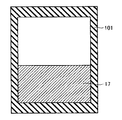
図2に示すように、第1の原料17として研磨用SiC粉末(GC)を準備する。GCは、たとえば入手可能な市販のものを用いる。準備した第1の原料17を坩堝101の下部に設置する。
As shown in FIG. 2, polishing SiC powder (GC) is prepared as the first
次に、図3に示すように、第1の原料17を加熱することにより昇華して、第1の原料17のガスから析出させることにより第1のSiC結晶11を成長する。原料としてGCを用いて第1のSiC結晶11を成長する場合には、種基板を配置しないことが好ましい。
Next, as shown in FIG. 3, the first
具体的には、第1の原料17が昇華する温度で、第1の原料17を加熱部により加熱する。この加熱により、第1の原料17が昇華して昇華ガスを生成する。この昇華ガスを、第1の原料17よりも低温に設置されている、坩堝101の内部において第1の原料と対向する位置、つまり坩堝101の上部に再度固化させる。
Specifically, the first
成長温度の一例を挙げると、たとえば、第1の原料17の温度を2000℃〜3000℃に保持し、第1の原料17と対向する位置の温度を1900℃〜2200℃で、かつ第1の原料17の温度よりも低くなるように保持する。また、坩堝101内部の雰囲気圧力は400Torr以下に保持することが好ましい。これにより、第1の原料17と対向する位置に第1のSiC結晶11が成長する。このように成長した第1のSiC結晶11は、たとえば多結晶である。
As an example of the growth temperature, for example, the temperature of the first
なお、第1の原料17の温度を2000℃以上にすると、第1のSiC結晶11の成長速度を高めることができる。第1の原料17の温度を3000℃以下にすると、坩堝101の損傷を抑制することができる。成長温度は、成長中に一定温度に保持する場合もあるが、成長中にある割合で変化させる場合もある。
If the temperature of the first
また、坩堝101の内部の雰囲気圧力を400Torr以下にすると、成長速度を高めることができる。
Further, when the atmospheric pressure inside the
次に、第1のSiC結晶11を粉砕して、第2の原料12(図5参照)を形成する。この工程では、たとえば以下のように行なう。具体的には、坩堝101の内部を室温まで冷却する。そして、坩堝101から成長した第1のSiC結晶11を取り出す。この第1のSiC結晶11をたとえば粉砕機などを用いて粉砕する。なお、粉砕する方法は、特に限定されない。
Next, the
この工程では、図4に示すように、1μm以上3mm以下の範囲に粒度分布のピークが複数(図4ではピークA、B、Cの3つ)あり、各々の粒度分布のピークA、B、Cの中心A1、B1、C1から±50%の範囲に95%以上の粒子が存在するように、第2の原料12を形成することが好ましい。粒度分布のピークA、B、Cの中心A1、B1、C1が1μm以上3mm以下であり、かつ各々の粒度分布のピークA、B、Cの中心A1、B1、C1から±50%の範囲に95%以上の粒子が存在することによって、坩堝101に第2の原料12を充填したときの充填率を高めることができる。これにより、この第2の原料12を用いて第2のSiC結晶14を成長するときの成長時間が短くなり、成長時に昇華した第2の原料12のガス濃度に影響が生じることを抑制できる。このため、この第2の原料12を用いて成長する第2のSiC結晶14の品質を高めることができる。
In this step, as shown in FIG. 4, there are a plurality of particle size distribution peaks (three peaks A, B, and C in FIG. 4) in the range of 1 μm to 3 mm, and each of the particle size distribution peaks A, B, It is preferable to form the second
このような観点から、最小粒度のピークAの中心A1が1μm以上100μm以下であり、最大粒度のピークCの中心C1が200μm以上3mm以下に存在するように、第2の原料12を形成することが好ましい。同様に、ピークAは10重量%以上50重量%以下の粒子を含み、ピークCは30重量%以上80重量%以下の粒子を含み、残部が他のピーク(図4ではピークB)である第2の原料12を形成することがより一層好ましい。
From such a viewpoint, the second
ここで、上記「各々の粒度分布のピークA、B、Cの中心A1、B1、C1から±50%の範囲に95%以上の粒子が存在する」とは、中心A1、B1、C1の粒径に対する150%の粒径A2、B2、C2と、中心A1、B1、C1の粒径に対する50%の粒径A3、B3、C3とのそれぞれの間に、第2の原料12の粒子全体の95%以上が存在することを意味する。なお、粒径分布のピークの数は、2つであっても、4以上であってもよい。
Here, “there is 95% or more of particles in the range of ± 50% from the centers A1, B1, and C1 of the peaks A, B, and C of each particle size distribution” means that the particles of the centers A1, B1, and C1 exist. Between the particle diameters A2, B2, C2 of 150% with respect to the diameter and the particle diameters A3, B3, C3 of 50% with respect to the particle diameters of the centers A1, B1, C1, the entire particles of the second
また、上記「粒度分布」は、たとえばJIS R6001 1998に準拠して測定される値である。 The “particle size distribution” is a value measured in accordance with, for example, JIS R6001 1998.
上記のような粒度分布を有する第2の原料12を形成する方法は特に限定されないが、たとえば第1のSiC結晶11を粉砕した後に、粒度分布が上記範囲になるように選択することにより、第2の原料12を形成することができる。なお、上記のような粒度分布を有するように第1のSiC結晶11を粉砕することにより、第2の原料12を形成してもよい。
The method of forming the second
また、第1のSiC結晶11を粉砕した後に、粉砕した第1のSiC結晶11を酸性溶液で洗浄することが好ましい。酸性溶液は、特に限定されないが、王水を用いることが好ましい。酸性溶液、特に王水を用いることにより、粉砕する際に第1のSiC結晶11に付着したFeなどの重金属を取り除くことができる。それに加えて、たとえば、塩酸で洗浄するとさらに好ましい。
Moreover, after pulverizing the
上記のように形成する第2の原料12は、0.1ppm以下の濃度のFeと、100ppm以下の濃度のAlとを含むことが好ましい。また上記のように形成した第2の原料12を坩堝101の下部に設置する。
The second
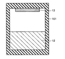
次に、図5に示すように、坩堝101内において、第2の原料12と対向するように、坩堝101の上部に種基板13を配置する。種基板13の主面の形状は、円形であっても、四角形であってもよい。また、種基板13の材料は特に限定されないが、成長する第2のSiC結晶14の品質を高める観点から、SiC基板であることが好ましく、成長するポリタイプ(結晶多形)と同一であることがより好ましい。たとえば、成長することを意図したSiC結晶が4H−SiCである場合には、種基板13も4H−SiCであることを意味する。なお、この工程は省略されてもよい。
Next, as shown in FIG. 5, in the
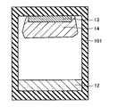
次に、図6に示すように、第2の原料12を加熱することにより昇華して、第2の原料12のガスから析出させることにより第2のSiC結晶14を成長する。本実施の形態では、第2のSiC結晶14は、種基板13上に成長する。第2のSiC結晶14は、単結晶であることが好ましい。第2のSiC結晶14の成長方法は、第1のSiC結晶11の成長方法とほぼ同じであるため、その説明は繰り返さない。
Next, as shown in FIG. 6, the second
次に、坩堝101の内部を室温まで冷却する。そして、坩堝101から、種基板13と、第2のSiC結晶14とを備えたインゴットを取り出す。このインゴットを図1に示すSiC結晶10としてもよい。つまり、第1の原料17を用いて第1のSiC結晶11を成長し、第1のSiC結晶11を粉砕して第2の原料12を形成し、第2の原料12を用いて第2のSiC結晶14を成長することにより、図1のSiC結晶10を製造してもよい。
Next, the inside of the
SiC結晶10の不純物をさらに低減するために、上記工程を繰り返すことが好ましい。つまり、第2のSiC結晶14を粉砕して、第3の原料を形成する工程と、第3の原料を加熱することにより昇華して、第3の原料のガスから析出させることにより第3のSiC結晶を成長する工程とをさらに実施することが好ましい。この1サイクルの工程により、たとえば約10%程度の不純物を低減することができる。
In order to further reduce impurities in
上記の工程を繰り返す程、成長するSiC結晶10の不純物濃度は低減されるが、半導体デバイスに用いるときに好ましいSiC結晶を製造する観点からは、成長したSiC結晶のFeの濃度が0.1ppm以下であり、かつAlの濃度が100ppm以下になるまで上記工程を繰り返すことが好ましい。またこのようなSiC結晶を確実に作製するために、Feの濃度が0.1ppm以下であり、かつAlの濃度が100ppm以下の原料を作製できるまで上記工程を繰り返し、この原料を用いてSiC結晶を成長することで、SiC結晶を製造することがより好ましい。
As the above steps are repeated, the impurity concentration of the grown
以上の工程を実施することにより、種基板と、種基板上に形成されたSiC結晶とを備えたインゴットを製造することができる。このインゴットを図1に示すSiC結晶10としてもよい。あるいは、インゴットから種基板13を除去することで、図1に示すSiC結晶10を製造してもよい。除去する場合には、種基板13のみを除去してもよく、種基板13および成長したSiC結晶の一部を除去してもよい。
By performing the above steps, an ingot including a seed substrate and an SiC crystal formed on the seed substrate can be manufactured. This ingot may be the
除去する方法は特に限定されず、たとえば切断、研削、へき開など機械的な除去方法を用いることができる。切断とは、たとえばワイヤーソーなどで機械的にインゴットから少なくとも種基板13を除去することをいう。研削とは、砥石を回転させながら表面に接触させて、厚さ方向に削り取ることをいう。へき開とは、結晶格子面に沿って結晶を分割することをいう。なお、エッチングなど化学的な除去方法を用いてもよい。
The removal method is not particularly limited, and a mechanical removal method such as cutting, grinding, or cleavage can be used. Cutting means that at least the
また、製造したSiC結晶10の厚さが大きい場合には、成長したSiC結晶から複数枚のSiC結晶を切り出すことで、図1に示すSiC結晶10を製造してもよい。この場合には、1枚当たりのSiC結晶10の製造コストを低減できる。
In addition, when the manufactured
その後、必要に応じて、SiC結晶の一方面または両面を研削、研磨などにより平坦化してもよい。 Thereafter, if necessary, one or both surfaces of the SiC crystal may be planarized by grinding, polishing, or the like.
以上説明したように、本発明の実施の形態におけるSiC結晶10の製造方法は、第1の原料17として研磨用SiC粉末を準備する工程と、第1の原料17を加熱することにより昇華させて、SiCの結晶を析出することにより、第1のSiC結晶11を成長する工程と、第1のSiC結晶11を粉砕して、第2の原料12を形成する工程と、第2の原料12を加熱することにより昇華させて、SiCの結晶を析出することにより、第2のSiC結晶14を成長する工程とを備えている。
As described above, the method for manufacturing
本発明者は、第1の原料17を用いて成長した第1のSiC結晶11を粉砕して第2の原料12を作製し、第2の原料12を用いて第2のSiC結晶14を成長すると、第2のSiC結晶14は第1のSiC結晶11よりもFeやAlなどの不純物を低減できるという知見を得ている。本実施の形態におけるSiC結晶10の製造方法によれば、第1の原料17としてGC原料を用いて第1のSiC結晶11を成長し、この第1のSiC結晶11を粉砕して第2の原料12を形成し、第2の原料12を用いて第2のSiC結晶14を成長している。このため、出発原料としてFeやAlの濃度が高いGCを用いても、第2のSiC結晶14は第1のSiC結晶11よりも不純物濃度を低減することができる。したがって、製造するSiC結晶10について、不純物に起因して品質が低下することを低減することができる。
The inventor pulverizes the
また、GCは容易に入手できるので、SiC結晶10の製造の工業化に有用である。このため、コストを低減してSiC結晶10を製造することができる。
Moreover, since GC is easily available, it is useful for industrialization of the production of the
このような本実施の形態におけるSiC結晶10の製造方法によれば、Feの濃度が0.1ppm以下であり、かつAlの濃度が100ppm以下であるSiC結晶10を製造することができる。本発明者は、SiC結晶10中のFeおよびAlの不純物濃度をどの範囲まで低減すれば、この不純物に起因した品質への影響が低減されるかについて鋭意研究した。その結果、FeおよびAlを上記範囲まで低減することにより、SiC結晶10の品質(たとえばマイクロパイプやエッチピットなどの結晶欠陥)への影響を低減できることを見い出した。したがって、本実施の形態のSiC結晶10によれば、品質の低下を抑制することができる。
According to the method for manufacturing
本実施例では、第1の原料17としてGCを用いて第1のSiC結晶11を成長し、第1のSiC結晶11を粉砕して第2の原料12を形成し、第2の原料12を用いて第2のSiC結晶14を成長することの効果について調べた。
In the present embodiment, the
(本発明例1)
本発明例1では、基本的には上述した実施の形態におけるSiC結晶の製造方法にしたがってSiC結晶を製造した。
(Invention Example 1)
In Example 1 of the present invention, an SiC crystal was basically manufactured according to the SiC crystal manufacturing method in the above-described embodiment.
具体的には、まず、第1の原料17として、一般に市販されている研磨材用のGCを準備した。この第1の原料を図2に示すように坩堝101の下部に配置するとともに、第1の原料17の最表面と対向する坩堝101の蓋には何も配置しなかった。
Specifically, first, as a first
次に、第1の原料17を加熱することにより昇華させて、第1の原料17のガスを析出させることにより第1のSiC結晶11を成長した。このとき、坩堝101の下部、つまり第1の原料17の温度は2300℃で、坩堝101の上部は2000℃とし、坩堝101の内部の圧力を1Torrとした。また、成長した第1のSiC結晶11は、多結晶であった。
Next, the first
次に、第1のSiC結晶11を粉砕した。粉砕は、粉砕機を用いて行なった。その後、粉砕した第1のSiC結晶11を王水で洗浄し、さらに塩酸で洗浄した。そして、粉砕した第1のSiC結晶11を用いて、図4に示すように、粒度分布のピークA、B、Cが3つあり、最小粒度のピークAの中心は1μm未満で、最大粒度のピークCの中心は3mmを超えるように、第2の原料12を形成した。また、各々の粒度分布のピークの中心から±50%の範囲に95%以上の粒子が存在するように第2の原料12を形成した。第2の原料12の粒度分布は、JIS R6001 1998に準拠して測定した。この第2の原料12を坩堝101内部の下部に配置した。
Next, the
次に、図5に示すように、種基板13として、マイクロパイプ密度が10個/cm2の4H−SiCを準備した。この種基板13を、坩堝101内部の上部において第2の原料12と対向するように、配置した。
Next, as shown in FIG. 5, 4H—SiC having a micropipe density of 10 pieces / cm 2 was prepared as a
次に、第2の原料12を加熱することにより昇華させて、第2の原料12のガスを析出させることにより第2のSiC結晶14を成長した。第2のSiC結晶14の成長方法は、第1のSiC結晶11の成長方法と同様とした。
Next, the second
以上の工程を実施することによって、本発明例1のSiC結晶を製造した。つまり、第2のSiC結晶14を本発明例1のSiC結晶とした。
The SiC crystal of Example 1 of the present invention was manufactured by performing the above steps. That is, the
(本発明例2)
本発明例2のSiC結晶の製造方法は、基本的には本発明例1と同様に製造したが、第2の原料12を形成する工程において、最大粒度のピークCの中心が200μm以上3mm以下の第2の原料12を形成した点において異なっていた。
(Invention Example 2)
The production method of the SiC crystal of Invention Example 2 was basically produced in the same manner as in Invention Example 1, but in the step of forming the second
(本発明例3)
本発明例3のSiC結晶の製造方法は、基本的には本発明例1と同様に製造したが、第2の原料12を形成する工程において、最小粒度のピークAの中心が1μm以上100μm以下の第2の原料12を形成した点において異なっていた。
(Invention Example 3)
The production method of the SiC crystal of Invention Example 3 was basically produced in the same manner as in Invention Example 1, but in the step of forming the second
(本発明例4)
本発明例4のSiC結晶の製造方法は、基本的には本発明例1と同様に製造したが、第2の原料12を形成する工程において、最小粒度のピークAの中心が1μm以上100μm以下で、かつ最大粒度のピークCの中心が200μm以上3mm以下の第2の原料12を形成した点において異なっていた。
(Invention Example 4)
The SiC crystal production method of Inventive Example 4 was basically produced in the same manner as in Inventive Example 1, but in the step of forming the second
(比較例1)
比較例1のSiC結晶の製造方法は、基本的には本発明例1と同様に製造したが、第1のSiC結晶11を粉砕して第2の原料を形成する工程を実施しなかった点において異なっていた。つまり、第1のSiC結晶11を比較例1のSiC結晶とした。
(Comparative Example 1)
The manufacturing method of the SiC crystal of Comparative Example 1 was basically manufactured in the same manner as Example 1 of the present invention, but the step of pulverizing the
(評価方法)
本発明例1〜4および比較例1のSiC結晶について、Alの濃度、Feの濃度、マイクロパイプ密度およびエッチピット密度を以下のように測定した。
(Evaluation method)
For the SiC crystals of Invention Examples 1 to 4 and Comparative Example 1, the Al concentration, the Fe concentration, the micropipe density, and the etch pit density were measured as follows.
AlおよびFeの濃度は、ICP(Inductive Coupled Plasma)−AES(Atomic Emission Spectrometry)(誘導結合プラズマ原子発光分析)により測定した。なお、Alの検出限界は0.02ppmであり、Feの検出限界は0.002ppmであった。 The concentrations of Al and Fe were measured by ICP (Inductive Coupled Plasma) -AES (Atomic Emission Spectrometry). The detection limit of Al was 0.02 ppm, and the detection limit of Fe was 0.002 ppm.
マイクロパイプ密度(MPD)は、本発明例1〜4および比較例1のSiC結晶を、種基板13と接していた面から10mm離れた面を有するようにスライスした後、500℃のKOH融液中に1〜10分浸し、エッチングされた表面についてノマルスキー微分干渉顕微鏡を用いてカウントされた貫通中空欠陥数から求めた。また、種基板13のマイクロパイプ密度に対して、種基板13上に成長したSiC結晶のマイクロパイプ密度(表1における結晶のMPD/種基板のMPD)も算出した。
The micropipe density (MPD) was determined by slicing the SiC crystals of Invention Examples 1 to 4 and Comparative Example 1 so as to have a
エッチピット密度(EPD)は、本発明例1〜4および比較例1のSiC結晶を、種基板13と接していた面から10mm離れた面を有するようにスライスした後、500℃のKOH融液中に1〜10分浸し、エッチングされた表面についてノマルスキー微分干渉顕微鏡を用いてカウントされたエッチピット数から求めた。
The etch pit density (EPD) was determined by slicing the SiC crystals of Invention Examples 1 to 4 and Comparative Example 1 so as to have a
これらの結果を下記の表1に示す。 These results are shown in Table 1 below.

(評価結果)
表1に示すように、第1の原料17を用いて第1のSiC結晶11を成長し、第1のSiC結晶11を粉砕して第2の原料12を形成し、第2の原料12を用いて第2のSiC結晶14を成長した本発明例1〜4は、比較例1よりもAlおよびFeの濃度を低減することができた。また、このように製造することで、0.1ppm以下の濃度のFeと、100ppm以下の濃度のAlとを含むSiC結晶を実現できることがわかった。
(Evaluation results)
As shown in Table 1, the
また、本発明例1〜4のSiC結晶は、比較例1のSiC結晶に比べて、マイクロパイプ密度およびエッチピット密度を低減できることがわかった。さらに、本発明例1〜4のSiC結晶は、比較例1のSiC結晶に比べて、種基板13のマイクロパイプを引き継ぐことが低減されることもわかった。
Moreover, it turned out that the SiC crystal of this invention example 1-4 can reduce a micropipe density and an etch pit density compared with the SiC crystal of the comparative example 1. FIG. Furthermore, it was also found that the SiC crystals of Examples 1 to 4 of the present invention reduced the inheritance of the micropipe of the
また、第2の原料を形成する工程において、1μm以上3mm以下の範囲に粒度分布のピークが複数あり、各々の粒度分布のピークの中心から±50%の範囲に95%以上の粒子が存在するように第2の原料を形成した本発明例4は、本発明例1〜3よりもマイクロパイプ密度およびエッチピット密度をより低減できることがわかった。また、種基板13のマイクロパイプを引き継ぐことがより低減されることもわかった。
Further, in the step of forming the second raw material, there are a plurality of particle size distribution peaks in the range of 1 μm or more and 3 mm or less, and 95% or more of particles exist in the range of ± 50% from the center of each particle size distribution peak. Thus, it was found that the present invention example 4 in which the second raw material was formed can reduce the micropipe density and the etch pit density more than the present invention examples 1 to 3. Moreover, it turned out that taking over the micropipe of the
以上より、本実施例によれば、第1の原料17を用いて第1のSiC結晶11を成長し、第1のSiC結晶11を粉砕して第2の原料12を形成し、第2の原料12を用いて第2のSiC結晶14を成長することにより、不純物を低減して品質の低下を抑制できることが確認できた。
As described above, according to the present embodiment, the
以上のように本発明の実施の形態について説明を行なったが、実施の形態の特徴を適宜組み合わせることも当初から予定している。また、今回開示された実施の形態はすべての点で例示であって制限的なものではないと考えられるべきである。本発明の範囲は上記した実施の形態ではなくて特許請求の範囲によって示され、特許請求の範囲と均等の意味および範囲内でのすべての変更が含まれることが意図される。 Although the embodiment of the present invention has been described above, it is also planned from the beginning to combine the features of the embodiment as appropriate. In addition, it should be considered that the embodiment disclosed this time is illustrative and not restrictive in all respects. The scope of the present invention is shown not by the above-described embodiment but by the scope of claims, and is intended to include all modifications within the meaning and scope equivalent to the scope of claims.
10 SiC結晶、11 第1のSiC結晶、12 第2の原料、13 種基板、14 第2のSiC結晶、17 第1の原料、101 坩堝、A、B、C ピーク、A1、B1、C1 中心、A2、A3、B2、B3、C2、C3 ピーク。 10 SiC crystal, 11 1st SiC crystal, 12 2nd raw material, 13 seed substrate, 14 2nd SiC crystal, 17 1st raw material, 101 crucible, A, B, C peak, A1, B1, C1 center , A2, A3, B2, B3, C2, C3 peaks.
Claims (6)
鉄の濃度が0.002ppm以上0.1ppm以下であり、かつアルミニウムの濃度が0.02ppm以上100ppm以下であり、マイクロパイプ密度が2個/cm2以下であり、
前記炭化珪素結晶は、種基板と、前記種基板上に成長する結晶成長部とを備え、前記種基板および前記結晶成長部の双方が4H−SiCであることを特徴とする、炭化珪素結晶。 In silicon carbide crystals,
The concentration of iron is lower than 0.1ppm least 0.002 ppm, and it is the concentration of the aluminum below 100ppm or 0.02 ppm, micropipe density Ri der 2 / cm 2 or less,
The silicon carbide crystal includes a seed substrate and a crystal growth portion that grows on the seed substrate, and both the seed substrate and the crystal growth portion are 4H—SiC .
前記第1の原料を加熱することにより昇華して、炭化珪素の結晶を析出することにより、第1の炭化珪素結晶を成長する工程と、
前記第1の炭化珪素結晶を粉砕して、第2の原料を形成する工程と、
前記第2の原料を加熱することにより昇華して、炭化珪素の結晶を析出することにより、第2の炭化珪素結晶を成長する工程とを備え、
前記第2の原料を形成する工程では、1μm以上3mm以下の範囲に粒度分布のピークが複数あり、各々の前記粒度分布のピークの中心の粒径から±50%の粒径の範囲に95%以上の粒子が存在するように前記第2の原料を形成する、炭化珪素結晶の製造方法。 Preparing a polishing silicon carbide powder as a first raw material;
A step of growing the first silicon carbide crystal by sublimating by heating the first raw material and precipitating a silicon carbide crystal;
Crushing the first silicon carbide crystal to form a second raw material;
A step of growing the second silicon carbide crystal by sublimating by heating the second raw material and precipitating a crystal of silicon carbide,
In the step of forming the second raw material, there are a plurality of particle size distribution peaks in the range of 1 μm or more and 3 mm or less, and 95% within the range of ± 50% particle size from the center particle size of each of the particle size distribution peaks. A method for producing a silicon carbide crystal, wherein the second raw material is formed so that the above particles are present.
前記第3の原料を加熱することにより昇華して、炭化珪素の結晶を析出することにより、第3の炭化珪素結晶を成長する工程とをさらに備えた、請求項3〜5のいずれか1項に記載の炭化珪素結晶の製造方法。 Crushing the second silicon carbide crystal to form a third raw material;
6. The method according to claim 3, further comprising a step of growing a third silicon carbide crystal by sublimating by heating the third raw material and precipitating a silicon carbide crystal. A method for producing a silicon carbide crystal as described in 1. above.
Priority Applications (10)
| Application Number | Priority Date | Filing Date | Title |
|---|---|---|---|
| JP2010100891A JP5565070B2 (en) | 2010-04-26 | 2010-04-26 | Silicon carbide crystal and method for producing silicon carbide crystal |
| PCT/JP2011/054339 WO2011135913A1 (en) | 2010-04-26 | 2011-02-25 | Silicon carbide crystal and method for producing silicon carbide crystal |
| US13/499,482 US8574529B2 (en) | 2010-04-26 | 2011-02-25 | Silicon carbide crystal and method of manufacturing silicon carbide crystal |
| CA2775923A CA2775923A1 (en) | 2010-04-26 | 2011-02-25 | Silicon carbide crystal and method of manufacturing silicon carbide crystal |
| KR1020127009040A KR20120130318A (en) | 2010-04-26 | 2011-02-25 | Silicon carbide crystal and method for producing silicon carbide crystal |
| CN2011800043891A CN102597339A (en) | 2010-04-26 | 2011-02-25 | Silicon carbide crystal and method for producing silicon carbide crystal |
| EP11774697.4A EP2565301B1 (en) | 2010-04-26 | 2011-02-25 | Silicon carbide crystal and method for producing silicon carbide crystal |
| TW100113266A TW201142092A (en) | 2010-04-26 | 2011-04-15 | Silicon carbide crystal and method for producing silicon carbide crystal |
| US14/019,882 US20140004303A1 (en) | 2010-04-26 | 2013-09-06 | Silicon carbide crystal and method of manufacturing silicon carbide crystal |
| US15/185,602 US9725823B2 (en) | 2010-04-26 | 2016-06-17 | Silicon carbide crystal and method of manufacturing silicon carbide crystal |
Applications Claiming Priority (1)
| Application Number | Priority Date | Filing Date | Title |
|---|---|---|---|
| JP2010100891A JP5565070B2 (en) | 2010-04-26 | 2010-04-26 | Silicon carbide crystal and method for producing silicon carbide crystal |
Publications (3)
| Publication Number | Publication Date |
|---|---|
| JP2011230941A JP2011230941A (en) | 2011-11-17 |
| JP2011230941A5 JP2011230941A5 (en) | 2013-01-24 |
| JP5565070B2 true JP5565070B2 (en) | 2014-08-06 |
Family
ID=44861234
Family Applications (1)
| Application Number | Title | Priority Date | Filing Date |
|---|---|---|---|
| JP2010100891A Active JP5565070B2 (en) | 2010-04-26 | 2010-04-26 | Silicon carbide crystal and method for producing silicon carbide crystal |
Country Status (8)
| Country | Link |
|---|---|
| US (3) | US8574529B2 (en) |
| EP (1) | EP2565301B1 (en) |
| JP (1) | JP5565070B2 (en) |
| KR (1) | KR20120130318A (en) |
| CN (1) | CN102597339A (en) |
| CA (1) | CA2775923A1 (en) |
| TW (1) | TW201142092A (en) |
| WO (1) | WO2011135913A1 (en) |
Families Citing this family (8)
| Publication number | Priority date | Publication date | Assignee | Title |
|---|---|---|---|---|
| JP5910393B2 (en) | 2012-07-26 | 2016-04-27 | 住友電気工業株式会社 | Method for manufacturing silicon carbide substrate |
| JP6028754B2 (en) | 2014-03-11 | 2016-11-16 | トヨタ自動車株式会社 | Method for manufacturing SiC single crystal substrate |
| US10108798B1 (en) * | 2016-01-04 | 2018-10-23 | Smart Information Flow Technologies LLC | Methods and systems for defending against cyber-attacks |
| CN105603530B (en) * | 2016-01-12 | 2018-02-27 | 台州市一能科技有限公司 | For the raw material of carborundum crystals high-speed rapid growth and the growing method of carborundum crystals |
| JP6086167B2 (en) * | 2016-03-18 | 2017-03-01 | 住友電気工業株式会社 | Method for manufacturing silicon carbide substrate |
| WO2018176302A1 (en) * | 2017-03-30 | 2018-10-04 | 新疆天科合达蓝光半导体有限公司 | Method and apparatus for preparing sic raw material for growing sic crystal |
| KR102442730B1 (en) * | 2021-12-23 | 2022-09-13 | 주식회사 쎄닉 | Silicon carbide powder, method for manufacturing silicon carbide ingot using the same, and silicon carbide wafer |
| KR102442731B1 (en) * | 2021-12-23 | 2022-09-13 | 주식회사 쎄닉 | silicon carbide powder and method for manufacturing silicon carbide ingot using the same |
Family Cites Families (19)
| Publication number | Priority date | Publication date | Assignee | Title |
|---|---|---|---|---|
| JPS58147493A (en) | 1982-02-12 | 1983-09-02 | フイリツプス・ペトロリユ−ム・コンパニ− | Antifoulant for thermal decomposition |
| JPS58187479A (en) | 1982-04-27 | 1983-11-01 | Honda Motor Co Ltd | Method for bonding outer covering material to flexible sealing material |
| JPH0645519B2 (en) * | 1986-08-18 | 1994-06-15 | 三洋電機株式会社 | Method for growing p-type SiC single crystal |
| JPS6350393A (en) * | 1986-08-20 | 1988-03-03 | Sanyo Electric Co Ltd | Growth method for sic single crystal |
| US5863325A (en) | 1995-05-31 | 1999-01-26 | Bridgestone Corporation | Process for producing high purity silicon carbide powder for preparation of a silicon carbide single crystal and single crystal |
| JP3934695B2 (en) * | 1995-05-31 | 2007-06-20 | 株式会社ブリヂストン | Method for producing high-purity silicon carbide powder for producing silicon carbide single crystal |
| JP3590464B2 (en) | 1995-12-08 | 2004-11-17 | 新日本製鐵株式会社 | Method for producing 4H type single crystal silicon carbide |
| US7553373B2 (en) * | 2001-06-15 | 2009-06-30 | Bridgestone Corporation | Silicon carbide single crystal and production thereof |
| SE520968C2 (en) * | 2001-10-29 | 2003-09-16 | Okmetic Oyj | High-resistance monocrystalline silicon carbide and its method of preparation |
| US20060249073A1 (en) | 2003-03-10 | 2006-11-09 | The New Industry Research Organization | Method of heat treatment and heat treatment apparatus |
| JP4593099B2 (en) * | 2003-03-10 | 2010-12-08 | 学校法人関西学院 | Liquid crystal epitaxial growth method of single crystal silicon carbide and heat treatment apparatus used therefor |
| JP4307913B2 (en) | 2003-06-18 | 2009-08-05 | 新日本製鐵株式会社 | Method for producing high-purity silicon carbide single crystal |
| JP2005239496A (en) * | 2004-02-27 | 2005-09-08 | Nippon Steel Corp | Silicon carbide raw material for growing silicon carbide single crystal, silicon carbide single crystal, and method for producing the same |
| JP4427470B2 (en) | 2004-03-29 | 2010-03-10 | 新日本製鐵株式会社 | Method for producing silicon carbide single crystal |
| EP1782454A4 (en) * | 2004-07-07 | 2009-04-29 | Ii Vi Inc | Low-doped semi-insulating sic crystals and method |
| JP2007284306A (en) * | 2006-04-19 | 2007-11-01 | Nippon Steel Corp | Silicon carbide single crystal and method for manufacturing the same |
| US9099377B2 (en) * | 2006-09-14 | 2015-08-04 | Cree, Inc. | Micropipe-free silicon carbide and related method of manufacture |
| JP2010083681A (en) * | 2008-09-29 | 2010-04-15 | Bridgestone Corp | Production method of silicon carbide single crystal and vacuum chuck |
| JP2010095397A (en) * | 2008-10-15 | 2010-04-30 | Nippon Steel Corp | Silicon carbide single crystal and silicon carbide single crystal wafer |
-
2010
- 2010-04-26 JP JP2010100891A patent/JP5565070B2/en active Active
-
2011
- 2011-02-25 KR KR1020127009040A patent/KR20120130318A/en not_active Application Discontinuation
- 2011-02-25 WO PCT/JP2011/054339 patent/WO2011135913A1/en active Application Filing
- 2011-02-25 US US13/499,482 patent/US8574529B2/en active Active
- 2011-02-25 CN CN2011800043891A patent/CN102597339A/en active Pending
- 2011-02-25 CA CA2775923A patent/CA2775923A1/en not_active Abandoned
- 2011-02-25 EP EP11774697.4A patent/EP2565301B1/en active Active
- 2011-04-15 TW TW100113266A patent/TW201142092A/en unknown
-
2013
- 2013-09-06 US US14/019,882 patent/US20140004303A1/en not_active Abandoned
-
2016
- 2016-06-17 US US15/185,602 patent/US9725823B2/en active Active
Also Published As
| Publication number | Publication date |
|---|---|
| EP2565301A1 (en) | 2013-03-06 |
| EP2565301A4 (en) | 2013-11-27 |
| CN102597339A (en) | 2012-07-18 |
| WO2011135913A1 (en) | 2011-11-03 |
| US20160289863A1 (en) | 2016-10-06 |
| EP2565301B1 (en) | 2015-03-25 |
| TW201142092A (en) | 2011-12-01 |
| US8574529B2 (en) | 2013-11-05 |
| JP2011230941A (en) | 2011-11-17 |
| KR20120130318A (en) | 2012-11-30 |
| CA2775923A1 (en) | 2011-11-03 |
| US20120183466A1 (en) | 2012-07-19 |
| US20140004303A1 (en) | 2014-01-02 |
| US9725823B2 (en) | 2017-08-08 |
Similar Documents
| Publication | Publication Date | Title |
|---|---|---|
| JP5565070B2 (en) | Silicon carbide crystal and method for producing silicon carbide crystal | |
| JP5706823B2 (en) | SiC single crystal wafer and manufacturing method thereof | |
| JP6037671B2 (en) | SiC epitaxial wafer and manufacturing method thereof | |
| CN107208311B (en) | Method for producing silicon carbide single crystal ingot, and silicon carbide single crystal ingot | |
| KR20130137247A (en) | Silicon carbide single crystal wafer and manufacturing method for same | |
| JP6624868B2 (en) | p-type low resistivity silicon carbide single crystal substrate | |
| JP6742183B2 (en) | Method for producing silicon carbide single crystal ingot | |
| JP2017065986A (en) | Method for manufacturing silicon carbide single crystal substrate having low resistivity | |
| JP2011162414A (en) | Method for producing silicon carbide crystal and silicon carbide crystal | |
| JP5674009B2 (en) | High hardness conductive diamond polycrystal and method for producing the same | |
| JP2016098162A (en) | Production method of reclaimed silicon carbide powder, and production method of silicon carbide single crystal | |
| JP6329733B2 (en) | Semiconductor wafer etching method, semiconductor wafer manufacturing method, and semiconductor wafer crystal defect detection method | |
| JP4494856B2 (en) | Seed crystal for silicon carbide single crystal growth, method for producing the same, and crystal growth method using the same | |
| JP5135545B2 (en) | Seed crystal for growing silicon carbide single crystal ingot and method for producing the same | |
| JP6304477B2 (en) | Silicon carbide powder and method for producing the same | |
| JP6695182B2 (en) | Method for producing seed crystal for growing silicon carbide single crystal and method for producing silicon carbide single crystal ingot | |
| US20240059570A1 (en) | Silicon carbide powder, method for manufacturing the same and method for manufacturing silicon carbide ingot using the same | |
| JP7298940B2 (en) | Silicon carbide wafer and manufacturing method thereof | |
| KR102236397B1 (en) | Silicon carbide wafer and semiconductor device applied the same | |
| KR102567936B1 (en) | silicon carbide powder, method for manufacturing the same and method for manufacturing silicon carbide ingot using the same | |
| KR102218607B1 (en) | Method of silicon carbide powder | |
| JP2011051861A (en) | METHOD FOR MANUFACTURING AlN SINGLE CRYSTAL AND SEED SUBSTRATE | |
| JP2011168425A (en) | Method for producing silicon carbide raw material and method for producing silicon carbide single crystal using the same | |
| JP2014015394A (en) | Method for producing silicon carbide crystal | |
| JP2015030659A (en) | Single crystal producing method |
Legal Events
| Date | Code | Title | Description |
|---|---|---|---|
| A621 | Written request for application examination |
Free format text: JAPANESE INTERMEDIATE CODE: A621 Effective date: 20121025 |
|
| A521 | Request for written amendment filed |
Free format text: JAPANESE INTERMEDIATE CODE: A523 Effective date: 20121129 |
|
| A131 | Notification of reasons for refusal |
Free format text: JAPANESE INTERMEDIATE CODE: A131 Effective date: 20140128 |
|
| A521 | Request for written amendment filed |
Free format text: JAPANESE INTERMEDIATE CODE: A523 Effective date: 20140325 |
|
| TRDD | Decision of grant or rejection written | ||
| A01 | Written decision to grant a patent or to grant a registration (utility model) |
Free format text: JAPANESE INTERMEDIATE CODE: A01 Effective date: 20140520 |
|
| A61 | First payment of annual fees (during grant procedure) |
Free format text: JAPANESE INTERMEDIATE CODE: A61 Effective date: 20140602 |
|
| R150 | Certificate of patent or registration of utility model |
Ref document number: 5565070 Country of ref document: JP Free format text: JAPANESE INTERMEDIATE CODE: R150 |
|
| R250 | Receipt of annual fees |
Free format text: JAPANESE INTERMEDIATE CODE: R250 |
|
| R250 | Receipt of annual fees |
Free format text: JAPANESE INTERMEDIATE CODE: R250 |
|
| R250 | Receipt of annual fees |
Free format text: JAPANESE INTERMEDIATE CODE: R250 |
|
| R250 | Receipt of annual fees |
Free format text: JAPANESE INTERMEDIATE CODE: R250 |
|
| R250 | Receipt of annual fees |
Free format text: JAPANESE INTERMEDIATE CODE: R250 |
|
| R250 | Receipt of annual fees |
Free format text: JAPANESE INTERMEDIATE CODE: R250 |
|
| R250 | Receipt of annual fees |
Free format text: JAPANESE INTERMEDIATE CODE: R250 |