EP2240965B1 - Feldeffekttransistor - Google Patents
Feldeffekttransistor Download PDFInfo
- Publication number
- EP2240965B1 EP2240965B1 EP08869339A EP08869339A EP2240965B1 EP 2240965 B1 EP2240965 B1 EP 2240965B1 EP 08869339 A EP08869339 A EP 08869339A EP 08869339 A EP08869339 A EP 08869339A EP 2240965 B1 EP2240965 B1 EP 2240965B1
- Authority
- EP
- European Patent Office
- Prior art keywords
- film
- atomic composition
- atom
- composition ratio
- tft
- Prior art date
- Legal status (The legal status is an assumption and is not a legal conclusion. Google has not performed a legal analysis and makes no representation as to the accuracy of the status listed.)
- Not-in-force
Links
- 230000005669 field effect Effects 0.000 title claims description 46
- 239000000203 mixture Substances 0.000 claims abstract description 148
- 229910052725 zinc Inorganic materials 0.000 claims abstract description 40
- 229910052738 indium Inorganic materials 0.000 claims abstract description 38
- 229910052718 tin Inorganic materials 0.000 claims abstract description 6
- 239000000758 substrate Substances 0.000 claims description 37
- 238000005401 electroluminescence Methods 0.000 claims description 13
- 239000004973 liquid crystal related substance Substances 0.000 claims description 8
- 229910052733 gallium Inorganic materials 0.000 claims description 5
- 229910052750 molybdenum Inorganic materials 0.000 claims description 4
- 210000002858 crystal cell Anatomy 0.000 claims description 3
- 239000010408 film Substances 0.000 description 161
- 239000011701 zinc Substances 0.000 description 87
- 239000010410 layer Substances 0.000 description 62
- 230000000052 comparative effect Effects 0.000 description 31
- 229910007541 Zn O Inorganic materials 0.000 description 28
- 239000010409 thin film Substances 0.000 description 26
- 238000000034 method Methods 0.000 description 24
- 230000007613 environmental effect Effects 0.000 description 22
- XLOMVQKBTHCTTD-UHFFFAOYSA-N Zinc monoxide Chemical compound [Zn]=O XLOMVQKBTHCTTD-UHFFFAOYSA-N 0.000 description 16
- 239000004065 semiconductor Substances 0.000 description 15
- 238000012552 review Methods 0.000 description 13
- 239000000463 material Substances 0.000 description 12
- 230000007423 decrease Effects 0.000 description 11
- 238000013461 design Methods 0.000 description 11
- QVGXLLKOCUKJST-UHFFFAOYSA-N atomic oxygen Chemical compound [O] QVGXLLKOCUKJST-UHFFFAOYSA-N 0.000 description 10
- 229910052799 carbon Inorganic materials 0.000 description 10
- PJXISJQVUVHSOJ-UHFFFAOYSA-N indium(iii) oxide Chemical compound [O-2].[O-2].[O-2].[In+3].[In+3] PJXISJQVUVHSOJ-UHFFFAOYSA-N 0.000 description 10
- 229910052751 metal Inorganic materials 0.000 description 10
- 229910052760 oxygen Inorganic materials 0.000 description 10
- 239000001301 oxygen Substances 0.000 description 10
- 239000011521 glass Substances 0.000 description 8
- 238000010438 heat treatment Methods 0.000 description 8
- JKQOBWVOAYFWKG-UHFFFAOYSA-N molybdenum trioxide Chemical compound O=[Mo](=O)=O JKQOBWVOAYFWKG-UHFFFAOYSA-N 0.000 description 8
- 238000004544 sputter deposition Methods 0.000 description 8
- 239000011787 zinc oxide Substances 0.000 description 8
- VYPSYNLAJGMNEJ-UHFFFAOYSA-N Silicium dioxide Chemical compound O=[Si]=O VYPSYNLAJGMNEJ-UHFFFAOYSA-N 0.000 description 7
- 230000015572 biosynthetic process Effects 0.000 description 7
- 239000002184 metal Substances 0.000 description 7
- 230000003247 decreasing effect Effects 0.000 description 6
- 238000011156 evaluation Methods 0.000 description 6
- 238000005259 measurement Methods 0.000 description 6
- 238000002441 X-ray diffraction Methods 0.000 description 5
- VVTSZOCINPYFDP-UHFFFAOYSA-N [O].[Ar] Chemical compound [O].[Ar] VVTSZOCINPYFDP-UHFFFAOYSA-N 0.000 description 5
- 238000004458 analytical method Methods 0.000 description 5
- 238000001636 atomic emission spectroscopy Methods 0.000 description 5
- 239000007789 gas Substances 0.000 description 5
- 239000012535 impurity Substances 0.000 description 5
- PXHVJJICTQNCMI-UHFFFAOYSA-N nickel Substances [Ni] PXHVJJICTQNCMI-UHFFFAOYSA-N 0.000 description 5
- 239000004033 plastic Substances 0.000 description 5
- 238000012546 transfer Methods 0.000 description 5
- 238000004876 x-ray fluorescence Methods 0.000 description 5
- 238000005516 engineering process Methods 0.000 description 4
- 150000002739 metals Chemical class 0.000 description 4
- 230000003287 optical effect Effects 0.000 description 4
- 238000000206 photolithography Methods 0.000 description 4
- ZOKXTWBITQBERF-UHFFFAOYSA-N Molybdenum Chemical compound [Mo] ZOKXTWBITQBERF-UHFFFAOYSA-N 0.000 description 3
- MWUXSHHQAYIFBG-UHFFFAOYSA-N Nitric oxide Chemical compound O=[N] MWUXSHHQAYIFBG-UHFFFAOYSA-N 0.000 description 3
- 239000003990 capacitor Substances 0.000 description 3
- 238000009826 distribution Methods 0.000 description 3
- 230000000694 effects Effects 0.000 description 3
- QZQVBEXLDFYHSR-UHFFFAOYSA-N gallium(III) oxide Inorganic materials O=[Ga]O[Ga]=O QZQVBEXLDFYHSR-UHFFFAOYSA-N 0.000 description 3
- 229910003437 indium oxide Inorganic materials 0.000 description 3
- 239000011733 molybdenum Substances 0.000 description 3
- 229910052759 nickel Inorganic materials 0.000 description 3
- 239000002245 particle Substances 0.000 description 3
- 229910052814 silicon oxide Inorganic materials 0.000 description 3
- 239000007787 solid Substances 0.000 description 3
- IJGRMHOSHXDMSA-UHFFFAOYSA-N Atomic nitrogen Chemical compound N#N IJGRMHOSHXDMSA-UHFFFAOYSA-N 0.000 description 2
- CURLTUGMZLYLDI-UHFFFAOYSA-N Carbon dioxide Chemical compound O=C=O CURLTUGMZLYLDI-UHFFFAOYSA-N 0.000 description 2
- 108091006149 Electron carriers Proteins 0.000 description 2
- GYHNNYVSQQEPJS-UHFFFAOYSA-N Gallium Chemical compound [Ga] GYHNNYVSQQEPJS-UHFFFAOYSA-N 0.000 description 2
- XUIMIQQOPSSXEZ-UHFFFAOYSA-N Silicon Chemical compound [Si] XUIMIQQOPSSXEZ-UHFFFAOYSA-N 0.000 description 2
- HCHKCACWOHOZIP-UHFFFAOYSA-N Zinc Chemical compound [Zn] HCHKCACWOHOZIP-UHFFFAOYSA-N 0.000 description 2
- 238000000862 absorption spectrum Methods 0.000 description 2
- 239000012790 adhesive layer Substances 0.000 description 2
- 230000008901 benefit Effects 0.000 description 2
- 230000005540 biological transmission Effects 0.000 description 2
- 210000004027 cell Anatomy 0.000 description 2
- 229910052681 coesite Inorganic materials 0.000 description 2
- 238000010835 comparative analysis Methods 0.000 description 2
- 229910052906 cristobalite Inorganic materials 0.000 description 2
- 238000001514 detection method Methods 0.000 description 2
- 238000000313 electron-beam-induced deposition Methods 0.000 description 2
- 238000002474 experimental method Methods 0.000 description 2
- APFVFJFRJDLVQX-UHFFFAOYSA-N indium atom Chemical compound [In] APFVFJFRJDLVQX-UHFFFAOYSA-N 0.000 description 2
- 229910052757 nitrogen Inorganic materials 0.000 description 2
- BASFCYQUMIYNBI-UHFFFAOYSA-N platinum Chemical compound [Pt] BASFCYQUMIYNBI-UHFFFAOYSA-N 0.000 description 2
- 238000001552 radio frequency sputter deposition Methods 0.000 description 2
- 229910052710 silicon Inorganic materials 0.000 description 2
- 239000010703 silicon Substances 0.000 description 2
- 239000000377 silicon dioxide Substances 0.000 description 2
- 229910052682 stishovite Inorganic materials 0.000 description 2
- 230000001629 suppression Effects 0.000 description 2
- 229910052905 tridymite Inorganic materials 0.000 description 2
- 239000012808 vapor phase Substances 0.000 description 2
- 229920002799 BoPET Polymers 0.000 description 1
- VYZAMTAEIAYCRO-UHFFFAOYSA-N Chromium Chemical compound [Cr] VYZAMTAEIAYCRO-UHFFFAOYSA-N 0.000 description 1
- CBENFWSGALASAD-UHFFFAOYSA-N Ozone Chemical compound [O-][O+]=O CBENFWSGALASAD-UHFFFAOYSA-N 0.000 description 1
- OAICVXFJPJFONN-UHFFFAOYSA-N Phosphorus Chemical compound [P] OAICVXFJPJFONN-UHFFFAOYSA-N 0.000 description 1
- 229910052581 Si3N4 Inorganic materials 0.000 description 1
- ATJFFYVFTNAWJD-UHFFFAOYSA-N Tin Chemical compound [Sn] ATJFFYVFTNAWJD-UHFFFAOYSA-N 0.000 description 1
- RTAQQCXQSZGOHL-UHFFFAOYSA-N Titanium Chemical compound [Ti] RTAQQCXQSZGOHL-UHFFFAOYSA-N 0.000 description 1
- 230000002411 adverse Effects 0.000 description 1
- 229910052782 aluminium Inorganic materials 0.000 description 1
- XAGFODPZIPBFFR-UHFFFAOYSA-N aluminium Chemical compound [Al] XAGFODPZIPBFFR-UHFFFAOYSA-N 0.000 description 1
- PNEYBMLMFCGWSK-UHFFFAOYSA-N aluminium oxide Inorganic materials [O-2].[O-2].[O-2].[Al+3].[Al+3] PNEYBMLMFCGWSK-UHFFFAOYSA-N 0.000 description 1
- 229910052793 cadmium Inorganic materials 0.000 description 1
- 239000002775 capsule Substances 0.000 description 1
- 229910002092 carbon dioxide Inorganic materials 0.000 description 1
- 239000001569 carbon dioxide Substances 0.000 description 1
- 229910052804 chromium Inorganic materials 0.000 description 1
- 239000011651 chromium Substances 0.000 description 1
- 239000000470 constituent Substances 0.000 description 1
- 229910052802 copper Inorganic materials 0.000 description 1
- 238000000151 deposition Methods 0.000 description 1
- 239000012530 fluid Substances 0.000 description 1
- 230000009477 glass transition Effects 0.000 description 1
- PCHJSUWPFVWCPO-UHFFFAOYSA-N gold Chemical compound [Au] PCHJSUWPFVWCPO-UHFFFAOYSA-N 0.000 description 1
- 229910052737 gold Inorganic materials 0.000 description 1
- 239000010931 gold Substances 0.000 description 1
- 239000011229 interlayer Substances 0.000 description 1
- 238000005468 ion implantation Methods 0.000 description 1
- 150000002500 ions Chemical class 0.000 description 1
- 238000003475 lamination Methods 0.000 description 1
- 229910052744 lithium Inorganic materials 0.000 description 1
- 229910052748 manganese Inorganic materials 0.000 description 1
- 238000004519 manufacturing process Methods 0.000 description 1
- 239000011159 matrix material Substances 0.000 description 1
- 229910052763 palladium Inorganic materials 0.000 description 1
- 229910052698 phosphorus Inorganic materials 0.000 description 1
- 239000011574 phosphorus Substances 0.000 description 1
- 239000002985 plastic film Substances 0.000 description 1
- 229920006255 plastic film Polymers 0.000 description 1
- 229910052697 platinum Inorganic materials 0.000 description 1
- 239000011347 resin Substances 0.000 description 1
- 229920005989 resin Polymers 0.000 description 1
- HQVNEWCFYHHQES-UHFFFAOYSA-N silicon nitride Chemical compound N12[Si]34N5[Si]62N3[Si]51N64 HQVNEWCFYHHQES-UHFFFAOYSA-N 0.000 description 1
- 229910052708 sodium Inorganic materials 0.000 description 1
- 230000003746 surface roughness Effects 0.000 description 1
- 229910052719 titanium Inorganic materials 0.000 description 1
- 239000010936 titanium Substances 0.000 description 1
- XLYOFNOQVPJJNP-UHFFFAOYSA-N water Chemical compound O XLYOFNOQVPJJNP-UHFFFAOYSA-N 0.000 description 1
- RUDFQVOCFDJEEF-UHFFFAOYSA-N yttrium(III) oxide Inorganic materials [O-2].[O-2].[O-2].[Y+3].[Y+3] RUDFQVOCFDJEEF-UHFFFAOYSA-N 0.000 description 1
Images


Classifications
-
- H—ELECTRICITY
- H01—ELECTRIC ELEMENTS
- H01L—SEMICONDUCTOR DEVICES NOT COVERED BY CLASS H10
- H01L29/00—Semiconductor devices adapted for rectifying, amplifying, oscillating or switching, or capacitors or resistors with at least one potential-jump barrier or surface barrier, e.g. PN junction depletion layer or carrier concentration layer; Details of semiconductor bodies or of electrodes thereof ; Multistep manufacturing processes therefor
- H01L29/66—Types of semiconductor device ; Multistep manufacturing processes therefor
- H01L29/68—Types of semiconductor device ; Multistep manufacturing processes therefor controllable by only the electric current supplied, or only the electric potential applied, to an electrode which does not carry the current to be rectified, amplified or switched
- H01L29/76—Unipolar devices, e.g. field effect transistors
- H01L29/772—Field effect transistors
- H01L29/78—Field effect transistors with field effect produced by an insulated gate
- H01L29/786—Thin film transistors, i.e. transistors with a channel being at least partly a thin film
- H01L29/7869—Thin film transistors, i.e. transistors with a channel being at least partly a thin film having a semiconductor body comprising an oxide semiconductor material, e.g. zinc oxide, copper aluminium oxide, cadmium stannate
Definitions
- the present invention relates to an amorphous (also known as non-crystalline) oxide and a field effect transistor in which such an amorphous oxide is used for an active layer.
- the present invention also relates to a display apparatus in which organic EL or inorganic EL using such a transistor is used as a light-emitting device and to a display apparatus in which liquid crystal using such a transistor is used.
- TFT transparent thin film transistor
- Japanese Patent Application Laid-Open No. 2002-76356 discloses a technology with regard to a TFT in which an oxide film mainly formed of Zn-O is used as an active layer.
- Journal of Non-Crystalline Solids 352 (2006) 2311 discloses that an oxide thin film formed at room temperature and mainly formed of indium oxide is used as a channel layer (active layer) of a TFT.
- the field-effect mobility of the TFT is 10 to 140 cm 2 /Vs and the S value of the TFT is 0.09 to 5.6 V/decade.
- United States Patent Application Publication No. 2006/0108636 discloses a technology with regard to addition of an impurity such as Li, Na, Mn, Ni, Pd, Cu, Cd, C, N, or P to an active layer of a TFT in which an amorphous oxide film formed at room temperature and containing indium, zinc, and gallium is used as an active layer.
- an impurity such as Li, Na, Mn, Ni, Pd, Cu, Cd, C, N, or P
- an active layer of a TFT in which an amorphous oxide film formed at room temperature and containing indium, zinc, and gallium is used as an active layer.
- the TFT disclosed in " Nature", Vol. 432, 25, November 2004 (pp- 488-492 ) has a problem that, depending on the atomic composition ratios of the metallic elements mainly forming the non-crystalline oxide film used as the active layer, the TFT characteristics vary greatly.
- the environmental stability of the In-O film formed at room temperature is low, and the resistivity of the In-O film varies greatly when the In-O film is left in an atmosphere.
- the resistivity is observed to decrease by one or two orders of magnitude.
- the above-mentioned decrease in resistivity is similarly observed in the oxide semiconductor disclosed in Japanese Patent Application Laid-Open No. 2002-76356 mainly formed of Zn-O.
- an object of the present invention is to provide a field-effect TFT which has excellent transistor characteristics including an excellent field-effect mobility and an excellent S value, excellent environmental stability, and a high margin of atomic composition ratios (degree of freedom of design).
- the present invention provides a field effect transistor as defined in claim 1 comprising. an amorphous oxide.
- the present invention provides a display apparatus as defined in claim 9.
- the field effect transistor which has excellent transistor characteristics including an excellent field-effect mobility and an excellent S value, and excellent environmental stability can be provided. Further, the field effect transistor which has a high margin of atomic composition ratios (degree of freedom of design) can be provided, which has the transistor characteristics with little variance depending on the atomic composition ratios of atoms (especially metallic atoms) forming the field effect transistor.
- the inventors of the present invention formed an In-Ga-Zn-O film at room temperature by a sputtering method and evaluated its transistor characteristics. It was found that, by making small the atomic composition ratio of Ga, a transistor which had excellent initial characteristics could be obtained. In particular, it was found that, when Ga was not contained in the oxide thin film, a transistor which had a high field-effect mobility and a small S value could be obtained.
- the S value as referred to herein means a gate voltage value in a sub-threshold region which changes a drain current by one order of magnitude with a constant drain voltage.
- the environmental stability of the oxide film itself varies. Variations over time of the resistivity when the oxide film is left at rest in the atmosphere become smaller as the atomic composition ratio of Ga in the film becomes higher. Specifically, from the viewpoint of TFT characteristics, it is preferred that the atomic composition ratio of Ga be low, while, from the viewpoint of environmental stability, it is preferred that the atomic composition ratio of Ga be high.
- the inventors of the present invention added various kinds of elements to an In-Zn-O film and measured variations over time of the transistor characteristics and the resistivity. As a result, it was found that, by adding a certain atomic composition ratio of Mo, the environmental stability could be improved while the transistor characteristics as good as those of an In-Zn-O film were maintained.
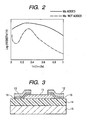
- FIG. 1 is a graph illustrating variations over time of the resistivity of the In-Zn-O film which is left in an atmosphere at a temperature of 20°C and at a humidity of 50%.
- the resistivity was observed to decrease immediately after the film formation.
- the atomic composition ratio of In was 55 atom% or higher and 30 atom% or lower, the environmental stability was low, and, depending on the atomic composition ratio, the resistivity decreased by one order to three orders of magnitude. Although the reason is not clear, it is thought that an excessive amount of a carrier was generated in the film, since the resistivity of the film greatly decreased.
- FIG. 2 is a graph of resistivity after the film was left at rest for one month, which is plotted against atomic composition ratio.
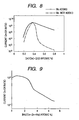
- FIG. 3 is a schematic view illustrating a structure of a TFT device according to this embodiment.
- the TFT is formed by providing a gate insulating film 14 on a gate electrode 15 and providing a source electrode 12 and a drain electrode 13 on the gate insulating film 14.
- the gate electrode 15 may also serve as a substrate by being formed of, for example, phosphorus doped Si, or may be formed on a substrate such as glass.
- the structure of the semiconductor device applicable to this embodiment is not limited to such an inverted staggered (bottom-gate) structure of the TFT, and may be a staggered structure (top-gate structure) of the TFT in which, for example, a gate insulating film and a gate electrode are provided in this order on an active layer as illustrated in FIG. 4 .
- an amorphous oxide which contains at least one element among In, Zn, and Sn and also contains a minute amount of Mo is used.
- the variations over time of the resistivity of the amorphous oxide are suppressed when the atomic composition ratio of Mo to the number of all metallic atoms in the amorphous oxide is 0.1 atom% or higher, and thus, a TFT which has excellent stability over time can be obtained by using the oxide as the active layer of the TFT.
- FIG. 5 is a graph of rate of change of the resistivity which is plotted against atomic composition ratio of Mo in the film. Specifically, values calculated by dividing the resistivity immediately after the film formation of the amorphous oxide formed with various atomic composition ratios of Mo by the resistivity after being left at rest in the atmosphere for a month are shown. FIG. 5 makes it clear that there is almost no variation of the resistivity in a film formed of an amorphous oxide in which the atomic composition ratio of Mo is 0.1 atom% or higher.
- the range of the atomic composition ratio of Mo to the number of all metallic atoms is preferably from 0.1 atom% to 5 atom%, and.more preferably, from 0.1 atom% to 3 atom%.
- the current on/off ratio can be determined from the ratio of the largest current (Id) between the source electrode and the drain electrode to the smallest Id in the transfer characteristics. From the result of the transfer characteristics, a graph of ⁇ Id-Vg is prepared, and the field-effect mobility is derived from the slope of the graph.
- a TFT which has a high field-effect mobility and a small S value with excellent sub-threshold characteristics can be obtained.
- a TFT which has a high field-effect mobility can be obtained with a film containing a large amount of In
- a TFT which has a small S value can be obtained with a film containing a large amount of Zn.
- suitable composition a transistor which has desired characteristics can be obtained.
- the atomic composition ratio of Zn to the number of all metallic atoms is higher than 70 atom%, the film becomes polycrystalline and the surface roughness of the film becomes large.
- the atomic composition ratio of Zn to the number of all metallic atoms be 70 atom% or lower.
- the lower limit of the atomic composition ratio of Zn is not particularly limited insofar as the effect of the present invention is obtained, but, according to findings of the inventors of the present invention, it is preferred that the lower limit be 70 atom%.
- the above-mentioned oxide material may contain Ga so as not to adversely affect other characteristics. Containing Ga has the advantage of being able to control the optical characteristics of the film by the composition ratio of Ga. Specifically, introduction of Ga into the film increases the band gap, and thus, an amorphous oxide which is highly transparent to visible light can be obtained.
- the above-mentioned oxide may contain other impurities insofar as the impurities do not substantially affect film characteristics including the carrier mobility, the carrier density, and the band gap.
- the material for the source electrode 12, the drain electrode 13, and the gate electrode is not particularly limited, so long as the material has good electrical conductance and is capable of electrical connection with the channel layer.
- a material serving both as a gate electrode and a substrate like a phosphorus-doped silicon substrate, can be used.
- a transparent conductive film such as an indium oxide film doped with tin or a zinc oxide, or a metal film of gold, platinum, aluminum, nickel, molybdenum, and the like may also be used. According to review by the inventors of the present invention, when molybdenum is used as the source and drain electrodes, particularly satisfactory TFT characteristics can be obtained.
- the adhesive layer 16 formed of titanium, nickel, chromium, or the like for improving the adhesion disposed between the active layer and the electrodes, and between the gate electrode and the gate insulating film, but the adhesive layer 16 is not essential.
- the gate insulating film 14 in addition to a silicon oxide film, a silicon nitride film, and a silicon oxynitride film which are usually used, any of an alumina film and an yttria film which have high dielectric constant, and a film formed by lamination thereof may be used.
- a glass substrate, a metallic substrate, a plastic substrate, a plastic film, or the like can be used as a substrate 10 formed with each of the above-mentioned films depending on the heat-treatment conditions.
- a substrate such as a glass substrate, a plastic substrate, a PET film, or an Si substrate is prepared.
- an oxide semiconductor is formed by a vapor phase method such as a sputtering method, a pulse laser deposition method, or an electron beam deposition method, or a combination thereof.
- a vapor phase method such as a sputtering method, a pulse laser deposition method, or an electron beam deposition method, or a combination thereof.
- O 2 or the like is introduced in the vapor phase.
- a TFT in which an oxide semiconductor thin film is used as the active layer particularly satisfactory TFT characteristics are obtained when a semi-insulating oxide film which has an electrical resistivity of about 1 ⁇ cm to 100 k ⁇ cm is used.
- the electrical resistivity is lower than 1 ⁇ cm, the current on/off ratio of the TFT cannot be made large.
- the electrical resistivity is higher than 100 k ⁇ cm, the on-current cannot be made large.
- even when a gate voltage is applied current between the source electrode and the drain electrode cannot be switched on/off, and transistor operation is not observed.
- the partial pressure of oxygen in film formation is controlled. Specifically, by controlling the partial pressure of oxygen, mainly the amount of loss of oxygen in the thin film is controlled to control the electron carrier density.
- the film is formed by the sputtering method, typically, by forming the film with the partial pressure of oxygen to be introduced being about 0.001 Pa to 0.01 Pa, a semi-insulating thin film can be obtained.
- heat treatment be carried out with respect to the manufactured oxide.
- the upper limit of the temperature of the heat treatment may be set as appropriate, but is preferably below the glass transition temperature at which heat deformation of the substrate is caused.
- the heat treatment be carried out at 450°C or lower, and, when the substrate is a plastic substrate, it is preferred that the heat treatment be carried out at 200°C or lower. This makes stable the electrical characteristics of the oxide film, and a more reliable semiconductor device can be materialized.
- the atmosphere contain any of oxygen, nitrogen, water vapor, carbon dioxide, ozone, and a nitrogen oxide and the temperature of the atmosphere is 150°C or higher (the upper limit of the temperature is adjusted to be within the above-mentioned range depending on the substrate to be used). This has an effect that the off-current of the TFT can be made further smaller and the interface characteristics are improved, and thus, the S value can be made smaller.
- FIG. 6 illustrates typical characteristics of a thin film transistor according to this embodiment.
- the field-effect mobility can be determined from characteristics in a linear region or a saturation region.
- a graph of ⁇ Id-Vg is prepared from the result of the transfer characteristics, and the field-effect mobility is derived from the slope of the graph. The evaluation herein is made by this method unless otherwise stated.
- the current on/off ratio can be determined from the ratio of the largest Id to the smallest Id in the transfer characteristics.
- the TFT of this embodiment has a higher field-effect mobility and a smaller S value. Further, the TFT of this embodiment has a larger design range of the atomic composition ratio of a metallic element (range of atomic composition ratio applicable to transistor). Specifically, as illustrated in FIG.
- the TFT of this embodiment exhibits at all times excellent characteristics with stability, and the TFT characteristics vary only a little from immediately after the manufacture to after the TFT is left at rest in the atmosphere for a month.
- a display apparatus By connecting the drain electrode which is an output terminal of the field effect transistor of this embodiment to an electrode of a display device such as an organic or inorganic electroluminescence (EL) device or a liquid crystal device, a display apparatus can be formed.
- a display apparatus An exemplary specific structure of a display apparatus is described in the following with reference to sectional views of the display apparatus.
- a field effect transistor is formed on a base 111.
- the field effect transistor includes an active layer (channel layer) 112, a source electrode 113, a drain electrode 114, a gate insulating film 115, and a gate electrode 116.
- An electrode 118 is connected to the drain electrode 114 via an interlayer insulating layer 117.
- the electrode 118 is brought into contact with a light-emitting layer 119, and the light-emitting layer 119 is brought into contact with an electrode 120.
- This structure enables control of current which flows in the light-emitting layer 119 by current which flows from the source electrode 113 to the drain electrode 114 via a channel formed in the active layer 112.
- the electrode 118, the light-emitting layer 119, and the electrode 120 form an inorganic or organic electroluminescence device.
- the structure may be such that the drain electrode 114 is extended so as to also serve as the electrode 118 for applying voltage to a liquid crystal cell or electrophoretic particle cell 123 sandwiched between high-resistance films 121 and 122.
- the liquid crystal cell or the electrophoretic particle cell 123, the high-resistance films 121 and 122, the electrode 118, and the electrode 120 form a display device.
- Voltage applied to the display device can be controlled by the current which flows from the source electrode 113 to the drain electrode 114 via the channel formed in the active layer 112. Therefore, voltage applied to the display device can be controlled by voltage at the gate electrode 116 of the TFT.
- a display medium of the display device is a capsule in which a fluid and particles are encapsulated in an insulating film, the high-resistance films 121 and 122 are not necessary.
- the thin film transistor is represented by a thin film transistor of a staggered structure (top-gate structure), but the present invention is not limited thereto.
- top-gate structure top-gate structure
- the connection between the drain electrode as an output terminal of the thin film transistor and the display device is topologically identical, other structures such as a coplanar type are also possible.
- the pair of electrodes for driving the display device are provided in parallel with the base, but this embodiment is not limited thereto.
- any one or both of the electrodes may be provided so as to be perpendicular to the base.
- the display device is an EL device or a reflection type display device such as a reflection type liquid crystal device
- any one of the electrodes is required to be transparent to the wavelength of emitted light or reflected light.
- the display device is a transmission type display device such as a transmission type liquid crystal device
- both of the electrodes are required to be transparent to transmitted light.
- a transparent display device it is also possible to make transparent all the constituents, which enables formation of a transparent display device. Further, such a display device can be provided on a base having low heat resistance such as a plastic substrate made of resin that is lightweight, flexible, and transparent.
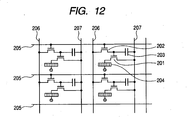
- FIG. 12 illustrates a transistor 201 for driving an organic EL layer 204 and a transistor 202 for selecting a pixel.
- a capacitor 203 is for holding a selected state, and charge is accumulated between a common electrode line 207 and a source portion of the transistor 202 and a signal at a gate of the transistor 201 is held.
- a pixel is selected by a scanning electrode line 205 and a signal electrode line 206.
- an image signal is applied as a pulse signal from a driver circuit (not shown) via the scanning electrode line 205 to a gate electrode.
- a pulse signal is applied from another driver circuit (not shown) via the signal electrode line 206 to the transistor 202 to select a pixel.
- the transistor 202 is turned ON, and charge is accumulated in the capacitor 203 disposed between the common electrode line 207 and the source of the transistor 202. This makes the gate voltage of the transistor 201 held at a desired voltage and the transistor 201 is turned ON. This state is held until a next signal is received.
- voltage and current continue to be supplied to the organic EL layer 204 to maintain light emission.
- two transistors and one capacitor are included in one pixel, but an additional transistor and the like may be incorporated therein to improve the performance.
- a first example of a TFT device according to the present invention is now described with reference to FIG. 4 .
- ITO was used as the gate electrode 15 and a silicon oxide film at a thickness of about 150 nm was used as the gate insulating film 14.
- the substrate was a glass substrate, and an In-Zn-O film with Mo added thereto was formed on the glass substrate as the active layer 11.
- a combinatorial method was used to form the film. Specifically, a technique in which a thin film of an oxide having various kinds of composition was manufactured on one substrate at a time by the sputtering method was used. However, it is not necessary to use this technique at any time.
- a material source (target) of predetermined composition may be prepared to form a thin film formed of an amorphous oxide, or, by controlling power applied to each of multiple targets, a thin film of a desired kind of composition may be formed.
- the In-Zn-O film with Mo added thereto was formed using a co-sputtering apparatus with diagonal incidence configuration.
- the target was disposed obliquely with respect to the substrate.
- the composition of the film on the surface of the substrate varied depending on the distance from the target, and hence a thin film having a wide composition distribution of the ternary elements across the surface of the substrate could be obtained.
- As the target (material source) a 2-inch sintered body with ZnO composition, a 2-inch sintered body with In 2 O 3 composition, and a 2-inch sintered body with MoO 3 composition (each at purity of 99.9%) were used.
- the applied RF power was 45 W with respect to ZnO, 35 W with respect to In 2 O 3 , and 11 W with respect to MoO 3 .
- the distance between the target and the substrate was about 7 to 12 cm, and the temperature of the substrate when the film was formed was 25°C.
- the In-Zn-O film with Mo added thereto was formed in an atmosphere of argon-oxygen mixed gas at 4 ⁇ 10 -1 Pa with the partial pressure of introduced oxygen being 6 ⁇ 10 -3 Pa .
- the sputtering method was used to form an ITO layer at a thickness of about 150 nm from a side nearer to the oxide semiconductor active layer, and, by a photolithography method and a lift-off method, the source electrode 12 and the drain electrode 13 were formed.
- an SiO 2 film used as the gate insulating film 14 was formed by an RF sputtering method at a thickness of about 200 nm, on which an ITO film was formed at a thickness of about 150 nm, and the gate electrode 15 was formed by the photolithography method and the lift-off method.
- the channel length was 10 ⁇ m and the channel width was 150 ⁇ m.
- X-ray diffraction was measured under the condition that the incident angle on the film surface was 0.5 degrees.
- the atomic composition ratio of Zn (Zn/(In+Zn+Mo)) was 70 atom% or lower, no clear diffraction peak was detected, and it was confirmed that the manufactured film was amorphous.
- the atomic composition ratio of Zn, Zn/(In+Zn+Mo) was 70 atom% or higher, a diffraction peak of Zn k In 2 O k+3 was detected, and it was confirmed that the manufactured film was crystallized.
- the structure was the same as that of the above-mentioned Example 1 except for the active layer.
- an In-Zn-O film without Mo added thereto was formed as the active layer 11. It is to be noted that, in this comparative example, also, in order to review the dependence of the material of the active layer on atomic composition ratio, the combinatorial method was used to form the film.
- the In-Zn-O film was formed in an atmosphere of argon-oxygen mixed gas at 4 ⁇ 10 -1 Pa with the partial pressure of introduced oxygen being 6 ⁇ 10 -3 Pa.
- Other conditions for film formation were the same as those of Example 1. Measurement with a profilometer was carried out with respect to the finally obtained oxide film. The film thickness was about 25 nm. Further, X-ray fluorescence analysis was carried out, and the atomic composition ratio of In, In/(Zn+In), was 15 to 80 atom%. With regard to evaluation of the amount of Mo in the film, ICP optical emission spectroscopy revealed that the amount of Mo was less than the detection limit.
- X-ray diffraction was measured under the condition that the incident angle on the film surface was 0.5 degrees.
- the atomic composition ratio of Zn, Zn/(In+Zn) was 70 atom% or higher, no clear diffraction peak was detected, and it was confirmed that the manufactured film was amorphous.
- the atomic composition ratio of Zn, Zn/(In+Zn) was 70 atom% or lower, a diffraction peak of Zn k In 2 O k+3 was detected, and it was confirmed that the manufactured film was crystallized.
- the structure was the same as that of the above-mentioned Example 1 except for the active layer.
- an In-Zn-O film with Mo added thereto was formed as the active layer 11, but the atomic composition ratio of Mo to the number of all metallic atoms was 0.01 to 0.05 atom%. It is to be noted that, in this comparative example, also, in order to review the dependence of the material of the active layer on atomic composition ratio, the combinatorial method was used to form the film.
- a 2-inch sintered body with ZnO composition As the target (material source), a 2-inch sintered body with ZnO composition, a 2-inch sintered body with In 2 O 3 composition, and a 2-inch sintered body with MoO 3 composition (each at purity of 99.9%) were used.
- the applied RF power was 80 W with respect to ZnO, 60 W with respect to In 2 O 3 , and 5 W with respect to MoO 3 .
- the distance between the target and the substrate was about 7 to 12 cm, and the temperature of the substrate when the film was formed was 25°C.
- the In-Zn-O film with Mo added thereto was formed in an atmosphere of argon-oxygen mixed gas at 4 ⁇ 10 -1 Pa with the partial pressure of introduced oxygen being 6 ⁇ 10 -3 Pa.
- Example 2 Other conditions for film formation were the same as those of Example 1. Measurement with a profilometer was carried out with respect to the finally obtained oxide film. The film thickness was 25 nm. Further, X-ray fluorescence analysis was carried out, and the atomic composition ratio of In, In/(Zn+In), was 15 to 80 atom%. With regard to evaluation of the amount of Mo in the film, ICP-optical emission spectroscopy revealed that the atomic composition ratio of Mo to the number of all metallic atoms Mo/(In+Zn+Mo) was about 0.01 to 0.05 atom%.
- X-ray diffraction was measured under the condition that the incident angle on the film surface was 0.5 degrees.
- the atomic composition ratio of Zn, Zn/(In+Zn) was 70 atom% or higher, no clear diffraction peak was detected, and it was confirmed that the manufactured film was amorphous.
- the atomic composition ratio of Zn, Zn/(In+Zn) was 70 atom% or lower, a diffraction peak of Zn k In 2 O k+3 was detected, and it was confirmed that the manufactured film was crystallized.
- Example 2 With regard to the In-Zn-O active layer with Mo added thereto obtained in Example 1, the optical absorption spectrum was analyzed. Band gap of the above-mentioned oxide film with Mo added thereto was about 2.7 to 2.9 eV depending on the atomic composition ratio of In, which is substantially the same as those of the In-Zn-O film of Comparative Example 1 and the In-Zn-O film with Mo added thereto of Comparative Example 2.
- Example 1 and Comparative Examples 1 and 2 were left at rest in an atmosphere at a temperature of 20°C and at a humidity of 50%, and the variations over time of the resistivity were measured.
- the oxide films of Comparative Examples 1 and 2 after being left at rest for a month, the resistivity decreased substantially by an order to two orders of magnitude depending on the atomic composition ratios of In and Zn, while, with regard to the In-Zn-O film with Mo added thereto of Example 1, decrease in resistivity was not observed, and it was found that the film had excellent environmental stability.
- FIG. 7 illustrates variations over time of the resistivity of the oxide films obtained in Example 1 and Comparative Examples 1 and 2 when the atomic composition ratio of In, In/(Zn+In), is 50 atom%.
- Example 1 satisfactory transistor characteristics were obtained when the atomic composition ratio of Mo to the number of all metallic atoms was 5 atom% or lower.
- FIG. 9 illustrates current on/off ratio of the TFT which is plotted against atomic composition ratio of Mo when the atomic composition ratio of In, In/(Zn+In), is 50 atom%.
- the value of the current on/off ratio was a three-digit number or more.
- the atomic composition ratio of Mo to the number of all metallic atoms was about 0.1 to 3 atom% and when the atomic composition ratio of In expressed as In/(Zn+In) was about 30 to 80 atom%.
- the obtained current on/off ratio was 10 5 or larger.
- the atomic composition ratio of In was 30 atom% or lower, the on-current was observed to greatly decrease, and, as a result, the current on/off ratio became smaller.
- the film was polycrystallized, and hence the above-mentioned decrease in on-current is thought to be due to lowered field-effect mobility which is in turn due to decrease in interface characteristics.
- FIG. 8 is a graph of TFT current on/off ratios with regard to Example 1 and Comparative Example 1. It is to be noted that the graph with regard to Example 1 of FIG. 8 was based on data obtained when the atomic composition ratio of Mo to the number of all metallic atoms was 0.1 atom%. As is clear from this figure, the current on/off ratio in Example 1 is extremely stable compared with that in Comparative Example 1.
- the TFT devices were left at rest in an atmosphere at a temperature of 20°C and at a humidity of 50%, and the variations over time of the TFT characteristics were measured.
- the result was that, with regard to the TFT manufactured in Example 1, even after being left at rest for a month, variations in characteristics were not observed, and it was found that the TFT had excellent environmental stability.
- the threshold voltages changed to the negative side by about 0.5 V to 2 V. Further, in the In-rich region, increase in off-current was observed, and, as a result, it was found that the current on/off ratio decreased by an order to two orders of magnitude.
- a TFT device which has excellent transistor characteristics including an excellent mobility and an excellent S value, excellent environmental stability, and a high margin of atomic composition ratios (degree of freedom of design) can be materialized.
- FIG. 4 A second example of a TFT device according to the present invention is now described with reference to FIG. 4 .
- an In-Zn-Ga-O film was used as the active layer.
- Mo was used as the gate electrode 15 and a silicon oxide film at a thickness of about 150 nm was used as the gate insulating film 14.
- the substrate was a glass substrate, and the In-Zn-Ga-O film with Mo added thereto was formed on the glass substrate as the active layer 11.
- the In-Zn-Ga-O film was formed using a co-sputtering apparatus with diagonal incidence configuration.
- a Ga concentration distribution was formed in a direction orthogonal to the composition slope of In-Zn.
- a 2-inch sintered body with ZnO composition As the target (material source), a 2-inch sintered body with ZnO composition, a 2-inch sintered body with In 2 O 3 composition, and a 2-inch sintered body with Ga 2 O 3 composition (each at purity of 99.9%) were used.
- the applied RF power was 50 W with respect to ZnO, 30 W with respect to In 2 O 3 , and 10 W with respect to Ga 2 O 3 .
- the In-Zn-Ga-O film was formed in an atmosphere of argon-oxygen mixed gas at 4 ⁇ 10 -1 Pa with the partial pressure of introduced oxygen being 1 ⁇ 10 -3 Pa. Further, after the In-Zn-Ga-O film was formed, Mo ions were implanted to add Mo.
- the sputtering method was used to form an ITO layer at a thickness of about 150 nm from a side nearer to the semiconductor active layer formed of the amorphous oxide. Then, by a photolithography method and a lift-off method, the source electrode 12 and the drain electrode 13 were formed. Finally, an SiO 2 film used as the gate insulating film 14 was formed by an RF sputtering method at a thickness of about 200 nm, on which an ITO film was formed at a thickness of about 150 nm, and the gate electrode 15 was formed by the photolithography method and the lift-off method. The channel length was 10 ⁇ m and the channel width was 150 ⁇ m.
- X-ray diffraction was measured under the condition that the incident angle on the film surface was 0.5 degrees.
- the atomic composition ratio of Zn, Zn/(In+Zn+Ga) was about 70 atom% or lower, no clear diffraction peak was detected, and it was confirmed that the manufactured film was amorphous.
- the atomic composition ratio of Zn, Zn/(In+Zn+Ga) was about 70 atom% or higher, a diffraction peak of InGaZn k O k+3 was detected, and it was confirmed that the manufactured film was crystallized.
- the structure was the same as that of the above-mentioned Example 2 except for the active layer.
- an In-Zn-Ga-O film without Mo added thereto was formed as the active layer 11.
- the combinatorial method was used to form the film.
- the In-Zn-Ga-O film was formed in an atmosphere of argon-oxygen mixed gas at 4 ⁇ 10 -1 Pa with the partial pressure of introduced oxygen being 1.5 ⁇ 10 -3 Pa. It is to be noted that, in this comparative example, Mo was not introduced to the oxide film by ion implantation. Other conditions for film formation were the same as those of Example 2. Measurement with a profilometer was carried out with respect to the finally obtained oxide film. The film thickness was about 25 nm. Further, X-ray fluorescence analysis was carried out, and the atomic composition ratio of In, In/(Zn+In), was 15 to 80 atom%. Further, it was found that the atomic composition ratio of Ga to all the atoms was about 1 to 10 atom%. With regard to evaluation of the amount of Mo in the film, ICP optical emission spectroscopy revealed that the amount of Mo was less than the detection limit.
- X-ray diffraction was measured under the condition that the incident angle on the film surface was 0.5 degrees.
- the atomic composition ratio of Zn, Zn/(In+Zn+Ga) was about 70 atom% or lower, no clear diffraction peak was detected, and it was confirmed that the manufactured film was amorphous.
- the atomic composition ratio of Zn, Zn/(In+Zn+Ga) was about 70 atom% or higher, a diffraction peak of InGaZn k O k+3 was detected, and it was confirmed that the manufactured film was crystallized.
- Example 2 With regard to the In-Zn-Ga-O active layer with Mo added thereto obtained in Example 2, the optical absorption spectrum was analyzed. Band gap of the above-mentioned oxide film with Mo added thereto was about 3 eV to 3.2 eV depending on the atomic composition ratio of a metal, which is higher than that of the In-Zn-O film with Mo added thereto of Example 1 and substantially the same as that of the In-Zn-Ga-O film of Comparative Example 3.
- the oxide film with Mo added thereto manufactured in Example 2 and the oxide film manufactured in Comparative Example 3 were left at rest in an atmosphere at a temperature of 20°C and at a humidity of 50%, and the variations over time of the resistivity were measured.
- the result was that, with regard to the In-Zn-Ga-O film with Mo added thereto in Example 2, variations in resistivity were not observed, and it was found that the In-Zn-Ga-O film had excellent environmental stability.
- Example 2 the most satisfactory transistor characteristics were obtained when the atomic composition ratio of Ga, Ga/(In+Ga+Zn), was 1 atom% and when the atomic composition ratio of In expressed as In/(Zn+In) was about 30 to 80 atom%.
- the atomic composition ratio of Ga, Ga/(In+Ga+Zn) was 1 atom% and when the atomic composition ratio of In expressed as In/(Zn+In) was about 30 to 80 atom%.
- substantially similar characteristics were obtained.
- the off-current Id was about 1 ⁇ 10 -14 A and the threshold voltage was about 1.8 V.
- the field-effect mobility was calculated from the output characteristics, in a saturation region, a value of about 13 cm 2 /Vs was obtained. The S value was about 0.4 V/dec.
- the atomic composition ratio of Ga As the atomic composition ratio of Ga became higher, the field-effect mobility was observed to be lowered and the S value was observed to increase. However, even when the atomic composition ratio of Ga, Ga/(In+Ga+Zn), was 10 atom%, the field-effect mobility was 10 cm 2 /Vs and the S value was 0.8 V/sec, which were relatively satisfactory values. Further, it was found that, here, the atomic composition ratio of In expressed as In/(Zn+In) when the transistor operated satisfactorily was about 26 atom% or higher and 83 atom% or lower, which is a wide range.
- the TFT device manufactured in Comparative Example 3 the most satisfactory transistor characteristics were obtained when the atomic composition ratio of In expressed as In/(Zn+In) was about 40 atom%.
- the mobility and the S value were about 11 to 13 cm 2 /Vs, and about 0.2 to 0.6 V/dec, respectively.
- increase in off-current with an increase in the atomic composition ratio of In was observed.
- the TFT devices were left at rest in an atmosphere at a temperature of 20°C and at a humidity of 50%, and the variations over time of the TFT characteristics were measured.
- the result was that, with regard to the TFT manufactured in Example 2, with respect to the TFTs having different atomic composition ratios of metals, even after being left at rest for a month, variations in characteristics were not observed, and it was found that the TFT had excellent environmental stability.
- TFT devices manufactured in Examples 1 and 2 variations in TFT characteristics when light from a fluorescent lamp was irradiated were reviewed.
- TFT in Example 1 it was found that the off-current increased to some extent, and, as a result, the current on/off ratio decreased.
- TFT in Example 2 it was found that variations in characteristics due to light irradiation from a fluorescent lamp were small, and, in particular, when the atomic composition ratio of Ga in the film was high, almost no variation of the characteristics was observed.
- a TFT device which has excellent transistor characteristics including an excellent mobility and an excellent S value, excellent environmental stability, and a high margin of atomic composition ratios (degree of freedom of design) can be materialized. Further, by selecting an appropriate concentration of Ga in the film, a TFT device which is highly transparent to visible light can be materialized.
- a TFT device having the same structure as that of the above-mentioned Example 2 except for the electrodes was manufactured.
- an Mo electrode at a thickness of about 100 nm formed by an electron beam deposition method was used as the gate electrode 15, the source electrode 12, and the drain electrode 13.
- the most satisfactory transistor characteristics were obtained when the atomic composition ratio of Ga, Ga/(In+Ga+Zn), was 1 atom% and when the atomic composition ratio of In expressed as In/(Zn+In) was about 30 to 80 atom%.
- the atomic composition ratio of Ga became higher, the field-effect mobility was observed to be lowered and the S value was observed to increase.
- the atomic composition ratio of Ga, Ga/(In+Ga+Zn) was 10 atom%, the field-effect mobility was 12 cm 2 /vs and the S value was 0.8 V/sec, which were relatively satisfactory values.
- the atomic composition ratio of In expressed as In/(Zn+In) when the transistor operates satisfactorily was as wide as about 26 atom% or higher and 83 atom% or lower.
Landscapes
- Engineering & Computer Science (AREA)
- Microelectronics & Electronic Packaging (AREA)
- Power Engineering (AREA)
- Physics & Mathematics (AREA)
- Ceramic Engineering (AREA)
- Condensed Matter Physics & Semiconductors (AREA)
- General Physics & Mathematics (AREA)
- Computer Hardware Design (AREA)
- Thin Film Transistor (AREA)
- Dram (AREA)
Claims (12)
- Feldeffektransistor, umfassend eine Drain-Elektrode (13), eine Source-Elektrode (12), eine Gate-Elektrode (15), eine aktive Schicht (11) und einen Gate-Isolationsfilm (14),
wobei die aktive Schicht ein amorphes Oxid beinhaltet, das Mo und zumindest ein Element ausgewählt aus der Gruppe bestehend aus In, Zn, und Sn enthält; und
ein Atomzusammensetzungsverhältnis (atomic composition ratio) von Mo zu einer Anzahl aller metallischen Atome in dem amorphen Oxid 0,1 Atom% oder höher und 5 Atom% oder niedriger ist. - Feldeffekttransistor nach Anspruch 1, wobei das Atomzusammensetzungsverhältnis von Mo zu der Anzahl aller metallischen Atome in dem amorphen Oxid 0,1 Atom% oder höher und 3 Atom% oder niedriger ist.
- Feldeffekttransistor nach Anspruch 1, umfassend In und Zn.
- Feldeffekttransistor nach Anspruch 3, wobei ein Atomzusammensetzungsverhältnis von In zu einer Summe von In und Zn, In/(In+Zn), in dem amorphen Oxid 30 Atom% oder höher und 80 Atom% oder niedriger ist.
- Feldeffekttransistor nach Anspruch 3, wobei ein Atomzusammensetzungsverhältnis von Zn zu der Anzahl aller metallischen Atome in dem amorphen Oxid 70 Atom% oder niedriger ist.
- Feldeffekttransistor nach einem der Ansprüche 1 bis 5, weiterhin umfassend Ga.
- Feldeffekttransistor nach einem der Ansprüche 1 bis 6, wobei die Source-Elektrode und die Drain-Elektrode Mo beinhalten.
- Feldeffekttransistor nach einem der Ansprüche 1 bis 6, wobei das amorphe Oxid einen spezifischen elektrischen Widerstand von 1 Ωcm bis 100 kΩcm hat.
- Anzeigevorrichtung, umfassend:Anzeigeeinrichtung mit Elektrode; undden Feldeffekttransistor nach einem der Ansprüche 1 bis 8, wobei von der Source-Elektrode und der Drain-Elektrode des Feldeffekttransistors eine Elektrode an eine Elektrode der Anzeigeeinrichtung angeschlossen ist.
- Anzeigevorrichtung nach Anspruch 9, wobei die Anzeigeeinrichtung eine Elektrolumineszenzeinrichtung umfasst.
- Anzeigevorrichtung nach Anspruch 9, wobei die Anzeigeeinrichtung eine Flüssigkristallzelle umfasst.
- Anzeigevorrichtung nach Anspruch 9, wobei mehrere der Anzeigeeinrichtungen und mehrere der Feldeffekttransistoren zweidimensional auf einem Substrat angeordnet sind.
Applications Claiming Priority (2)
| Application Number | Priority Date | Filing Date | Title |
|---|---|---|---|
| JP2008001336A JP5213458B2 (ja) | 2008-01-08 | 2008-01-08 | アモルファス酸化物及び電界効果型トランジスタ |
| PCT/JP2008/073924 WO2009087943A1 (en) | 2008-01-08 | 2008-12-25 | Amorphous oxide and field effect transistor |
Publications (2)
| Publication Number | Publication Date |
|---|---|
| EP2240965A1 EP2240965A1 (de) | 2010-10-20 |
| EP2240965B1 true EP2240965B1 (de) | 2011-07-20 |
Family
ID=40503360
Family Applications (1)
| Application Number | Title | Priority Date | Filing Date |
|---|---|---|---|
| EP08869339A Not-in-force EP2240965B1 (de) | 2008-01-08 | 2008-12-25 | Feldeffekttransistor |
Country Status (7)
| Country | Link |
|---|---|
| US (1) | US8212248B2 (de) |
| EP (1) | EP2240965B1 (de) |
| JP (1) | JP5213458B2 (de) |
| CN (1) | CN101911304B (de) |
| AT (1) | ATE517435T1 (de) |
| TW (1) | TWI433312B (de) |
| WO (1) | WO2009087943A1 (de) |
Families Citing this family (90)
| Publication number | Priority date | Publication date | Assignee | Title |
|---|---|---|---|---|
| TWI487104B (zh) * | 2008-11-07 | 2015-06-01 | Semiconductor Energy Lab | 半導體裝置和其製造方法 |
| JP2011066375A (ja) | 2009-08-18 | 2011-03-31 | Fujifilm Corp | 非晶質酸化物半導体材料、電界効果型トランジスタ及び表示装置 |
| JP5700626B2 (ja) | 2009-09-04 | 2015-04-15 | 株式会社半導体エネルギー研究所 | El表示装置 |
| JP5458102B2 (ja) * | 2009-09-04 | 2014-04-02 | 株式会社東芝 | 薄膜トランジスタの製造方法 |
| KR102337631B1 (ko) | 2009-09-24 | 2021-12-10 | 가부시키가이샤 한도오따이 에네루기 켄큐쇼 | 반도체 장치 및 그 제조 방법 |
| KR102321565B1 (ko) | 2009-09-24 | 2021-11-05 | 가부시키가이샤 한도오따이 에네루기 켄큐쇼 | 산화물 반도체막 및 반도체 장치 |
| WO2011043163A1 (en) | 2009-10-05 | 2011-04-14 | Semiconductor Energy Laboratory Co., Ltd. | Semiconductor device and manufacturing method thereof |
| WO2011043218A1 (en) | 2009-10-09 | 2011-04-14 | Semiconductor Energy Laboratory Co., Ltd. | Semiconductor device and method for manufacturing the same |
| KR101772639B1 (ko) | 2009-10-16 | 2017-08-29 | 가부시키가이샤 한도오따이 에네루기 켄큐쇼 | 반도체 장치 |
| CN113903796A (zh) | 2009-10-16 | 2022-01-07 | 株式会社半导体能源研究所 | 逻辑电路和半导体器件 |
| WO2011046010A1 (en) | 2009-10-16 | 2011-04-21 | Semiconductor Energy Laboratory Co., Ltd. | Liquid crystal display device and electronic device including the liquid crystal display device |
| CN103794612B (zh) * | 2009-10-21 | 2018-09-07 | 株式会社半导体能源研究所 | 半导体装置 |
| WO2011048968A1 (en) * | 2009-10-21 | 2011-04-28 | Semiconductor Energy Laboratory Co., Ltd. | Semiconductor device |
| CN112447130A (zh) * | 2009-10-21 | 2021-03-05 | 株式会社半导体能源研究所 | 显示装置和包括显示装置的电子设备 |
| SG10201910510UA (en) * | 2009-10-29 | 2020-01-30 | Semiconductor Energy Lab | Semiconductor device |
| EP2494594B1 (de) * | 2009-10-29 | 2020-02-19 | Semiconductor Energy Laboratory Co. Ltd. | Halbleiterbauelement |
| KR101752518B1 (ko) | 2009-10-30 | 2017-06-29 | 가부시키가이샤 한도오따이 에네루기 켄큐쇼 | 반도체 장치 |
| EP2494601A4 (de) | 2009-10-30 | 2016-09-07 | Semiconductor Energy Lab | Halbleiterbauelement und herstellungsverfahren dafür |
| KR20120091243A (ko) * | 2009-10-30 | 2012-08-17 | 가부시키가이샤 한도오따이 에네루기 켄큐쇼 | 반도체 장치 |
| CN102598249B (zh) | 2009-10-30 | 2014-11-05 | 株式会社半导体能源研究所 | 半导体装置 |
| MY163862A (en) * | 2009-10-30 | 2017-10-31 | Semiconductor Energy Lab | Logic circuit and semiconductor device |
| CN104485341A (zh) * | 2009-11-06 | 2015-04-01 | 株式会社半导体能源研究所 | 半导体装置 |
| CN104600074A (zh) * | 2009-11-06 | 2015-05-06 | 株式会社半导体能源研究所 | 半导体装置 |
| WO2011058882A1 (en) * | 2009-11-13 | 2011-05-19 | Semiconductor Energy Laboratory Co., Ltd. | Sputtering target and manufacturing method thereof, and transistor |
| JP5596963B2 (ja) * | 2009-11-19 | 2014-09-24 | 出光興産株式会社 | スパッタリングターゲット及びそれを用いた薄膜トランジスタ |
| CN102598266B (zh) * | 2009-11-20 | 2015-04-22 | 株式会社半导体能源研究所 | 半导体装置 |
| KR20200096317A (ko) | 2009-11-20 | 2020-08-11 | 가부시키가이샤 한도오따이 에네루기 켄큐쇼 | 반도체 장치 |
| EP2887395B1 (de) * | 2009-11-20 | 2019-05-08 | Semiconductor Energy Laboratory Co., Ltd. | Nichtflüchtige Sperrschaltung und Logikschaltung sowie Halbleiterbauelement damit |
| KR101790365B1 (ko) | 2009-11-20 | 2017-10-25 | 가부시키가이샤 한도오따이 에네루기 켄큐쇼 | 반도체 장치 |
| KR102089200B1 (ko) * | 2009-11-28 | 2020-03-13 | 가부시키가이샤 한도오따이 에네루기 켄큐쇼 | 반도체 장치 및 그 제조 방법 |
| WO2011068106A1 (en) * | 2009-12-04 | 2011-06-09 | Semiconductor Energy Laboratory Co., Ltd. | Display device and electronic device including the same |
| KR101804589B1 (ko) * | 2009-12-11 | 2018-01-10 | 가부시키가이샤 한도오따이 에네루기 켄큐쇼 | 반도체 장치 및 그 제조 방법 |
| WO2011070929A1 (en) | 2009-12-11 | 2011-06-16 | Semiconductor Energy Laboratory Co., Ltd. | Semiconductor device and electronic device |
| CN104658598B (zh) | 2009-12-11 | 2017-08-11 | 株式会社半导体能源研究所 | 半导体器件、逻辑电路和cpu |
| EP2513966B1 (de) * | 2009-12-18 | 2020-09-16 | Semiconductor Energy Laboratory Co., Ltd. | Halbleiterbauelement |
| WO2011074408A1 (en) | 2009-12-18 | 2011-06-23 | Semiconductor Energy Laboratory Co., Ltd. | Non-volatile latch circuit and logic circuit, and semiconductor device using the same |
| WO2011077916A1 (en) | 2009-12-24 | 2011-06-30 | Semiconductor Energy Laboratory Co., Ltd. | Display device |
| KR101777624B1 (ko) | 2009-12-25 | 2017-09-13 | 가부시키가이샤 한도오따이 에네루기 켄큐쇼 | 반도체 장치 |
| CN103985760B (zh) | 2009-12-25 | 2017-07-18 | 株式会社半导体能源研究所 | 半导体装置 |
| US8780629B2 (en) * | 2010-01-15 | 2014-07-15 | Semiconductor Energy Laboratory Co., Ltd. | Semiconductor device and driving method thereof |
| WO2011089844A1 (en) | 2010-01-24 | 2011-07-28 | Semiconductor Energy Laboratory Co., Ltd. | Display device and manufacturing method thereof |
| WO2011096270A1 (en) | 2010-02-05 | 2011-08-11 | Semiconductor Energy Laboratory Co., Ltd. | Semiconductor device |
| WO2011108346A1 (en) * | 2010-03-05 | 2011-09-09 | Semiconductor Energy Laboratory Co., Ltd. | Manufacturing method of oxide semiconductor film and manufacturing method of transistor |
| KR101840797B1 (ko) * | 2010-03-19 | 2018-03-21 | 가부시키가이샤 한도오따이 에네루기 켄큐쇼 | 반도체 메모리 장치 |
| WO2011114868A1 (en) | 2010-03-19 | 2011-09-22 | Semiconductor Energy Laboratory Co., Ltd. | Semiconductor device |
| JP5727832B2 (ja) * | 2010-03-31 | 2015-06-03 | 株式会社半導体エネルギー研究所 | トランジスタ |
| WO2011145467A1 (en) * | 2010-05-21 | 2011-11-24 | Semiconductor Energy Laboratory Co., Ltd. | Semiconductor device |
| WO2012002186A1 (en) | 2010-07-02 | 2012-01-05 | Semiconductor Energy Laboratory Co., Ltd. | Semiconductor device |
| US8422272B2 (en) | 2010-08-06 | 2013-04-16 | Semiconductor Energy Laboratory Co., Ltd. | Semiconductor device and driving method thereof |
| JP2012064201A (ja) * | 2010-08-19 | 2012-03-29 | Semiconductor Energy Lab Co Ltd | 入出力装置及び入出力装置の駆動方法 |
| JP2012256821A (ja) | 2010-09-13 | 2012-12-27 | Semiconductor Energy Lab Co Ltd | 記憶装置 |
| WO2012060253A1 (en) | 2010-11-05 | 2012-05-10 | Semiconductor Energy Laboratory Co., Ltd. | Semiconductor device |
| JP2012164963A (ja) | 2010-11-26 | 2012-08-30 | Kobe Steel Ltd | 薄膜トランジスタの半導体層用酸化物およびスパッタリングターゲット、並びに薄膜トランジスタ |
| JP5723262B2 (ja) | 2010-12-02 | 2015-05-27 | 株式会社神戸製鋼所 | 薄膜トランジスタおよびスパッタリングターゲット |
| JP2012151453A (ja) | 2010-12-28 | 2012-08-09 | Semiconductor Energy Lab Co Ltd | 半導体装置および半導体装置の駆動方法 |
| KR102026718B1 (ko) | 2011-01-14 | 2019-09-30 | 가부시키가이샤 한도오따이 에네루기 켄큐쇼 | 기억장치, 반도체 장치, 검출 방법 |
| JP2013153118A (ja) | 2011-03-09 | 2013-08-08 | Kobe Steel Ltd | 薄膜トランジスタの半導体層用酸化物、上記酸化物を備えた薄膜トランジスタの半導体層および薄膜トランジスタ |
| US8859330B2 (en) * | 2011-03-23 | 2014-10-14 | Semiconductor Energy Laboratory Co., Ltd. | Method for manufacturing semiconductor device |
| TWI567735B (zh) | 2011-03-31 | 2017-01-21 | 半導體能源研究所股份有限公司 | 記憶體電路,記憶體單元,及訊號處理電路 |
| JP2012235104A (ja) | 2011-04-22 | 2012-11-29 | Kobe Steel Ltd | 薄膜トランジスタ構造、ならびにその構造を備えた薄膜トランジスタおよび表示装置 |
| EP2715821A1 (de) * | 2011-06-01 | 2014-04-09 | Merck Patent GmbH | Hybride ambipolare tfts |
| JP5984354B2 (ja) * | 2011-10-07 | 2016-09-06 | 住友電気工業株式会社 | 半導体素子 |
| US9076505B2 (en) | 2011-12-09 | 2015-07-07 | Semiconductor Energy Laboratory Co., Ltd. | Memory device |
| JP6204036B2 (ja) | 2012-03-16 | 2017-09-27 | 株式会社神戸製鋼所 | 酸化物半導体薄膜の評価方法、及び酸化物半導体薄膜の品質管理方法 |
| US9208849B2 (en) | 2012-04-12 | 2015-12-08 | Semiconductor Energy Laboratory Co., Ltd. | Semiconductor device and method for driving semiconductor device, and electronic device |
| WO2013168748A1 (ja) | 2012-05-09 | 2013-11-14 | 株式会社神戸製鋼所 | 薄膜トランジスタおよび表示装置 |
| CN102751240B (zh) * | 2012-05-18 | 2015-03-11 | 京东方科技集团股份有限公司 | 薄膜晶体管阵列基板及其制造方法、显示面板、显示装置 |
| JP6068232B2 (ja) | 2012-05-30 | 2017-01-25 | 株式会社神戸製鋼所 | 薄膜トランジスタの半導体層用酸化物、薄膜トランジスタ、表示装置およびスパッタリングターゲット |
| JP6002088B2 (ja) | 2012-06-06 | 2016-10-05 | 株式会社神戸製鋼所 | 薄膜トランジスタ |
| US9202926B2 (en) | 2012-06-06 | 2015-12-01 | Kobe Steel, Ltd. | Thin film transistor |
| JP6059460B2 (ja) | 2012-07-20 | 2017-01-11 | 株式会社コベルコ科研 | ターゲット組立体 |
| JP6134230B2 (ja) | 2012-08-31 | 2017-05-24 | 株式会社神戸製鋼所 | 薄膜トランジスタおよび表示装置 |
| JP2014225626A (ja) | 2012-08-31 | 2014-12-04 | 株式会社神戸製鋼所 | 薄膜トランジスタおよび表示装置 |
| JP5722293B2 (ja) | 2012-10-19 | 2015-05-20 | 株式会社神戸製鋼所 | 薄膜トランジスタ |
| WO2014073374A1 (en) | 2012-11-06 | 2014-05-15 | Semiconductor Energy Laboratory Co., Ltd. | Semiconductor device and driving method thereof |
| JP6152348B2 (ja) | 2013-01-11 | 2017-06-21 | 株式会社神戸製鋼所 | 酸化物半導体薄膜の評価方法及び酸化物半導体薄膜の品質管理方法 |
| KR102112367B1 (ko) | 2013-02-12 | 2020-05-18 | 가부시키가이샤 한도오따이 에네루기 켄큐쇼 | 반도체 장치 |
| US9012261B2 (en) * | 2013-03-13 | 2015-04-21 | Intermolecular, Inc. | High productivity combinatorial screening for stable metal oxide TFTs |
| WO2014157019A1 (en) | 2013-03-25 | 2014-10-02 | Semiconductor Energy Laboratory Co., Ltd. | Semiconductor device |
| JP6516978B2 (ja) | 2013-07-17 | 2019-05-22 | 株式会社半導体エネルギー研究所 | 半導体装置 |
| JP5798669B2 (ja) | 2013-12-03 | 2015-10-21 | 株式会社神戸製鋼所 | 酸化物半導体薄膜の評価方法、及び酸化物半導体薄膜の品質管理方法、並びに上記評価方法に用いられる評価装置 |
| JP6442321B2 (ja) | 2014-03-07 | 2018-12-19 | 株式会社半導体エネルギー研究所 | 半導体装置及びその駆動方法、並びに電子機器 |
| WO2015170220A1 (en) | 2014-05-09 | 2015-11-12 | Semiconductor Energy Laboratory Co., Ltd. | Memory device and electronic device |
| JP6283273B2 (ja) | 2014-07-01 | 2018-02-21 | 株式会社神戸製鋼所 | 薄膜トランジスタ評価用の積層構造体の評価方法 |
| JP5993496B2 (ja) | 2014-07-16 | 2016-09-14 | 株式会社神戸製鋼所 | 酸化物半導体薄膜、及び前記酸化物半導体薄膜の表面に保護膜を有する積層体の品質評価方法、及び酸化物半導体薄膜の品質管理方法 |
| CN104716196B (zh) * | 2015-03-18 | 2017-08-08 | 京东方科技集团股份有限公司 | 薄膜晶体管及其制作方法、阵列基板及显示装置 |
| US9773787B2 (en) | 2015-11-03 | 2017-09-26 | Semiconductor Energy Laboratory Co., Ltd. | Semiconductor device, memory device, electronic device, or method for driving the semiconductor device |
| CN105977164A (zh) * | 2016-06-28 | 2016-09-28 | 京东方科技集团股份有限公司 | 一种薄膜晶体管及其制作方法、阵列基板和显示面板 |
| KR102458660B1 (ko) | 2016-08-03 | 2022-10-26 | 가부시키가이샤 한도오따이 에네루기 켄큐쇼 | 표시 장치 및 전자 기기 |
| JPWO2019102316A1 (ja) * | 2017-11-24 | 2020-12-10 | 株式会社半導体エネルギー研究所 | 酸化物半導体を有するトランジスタ |
Citations (1)
| Publication number | Priority date | Publication date | Assignee | Title |
|---|---|---|---|---|
| US20100276688A1 (en) * | 2007-12-25 | 2010-11-04 | Idemitsu Kosan Co., Ltd. | Oxide semiconductor field effect transistor and method for manufacturing the same |
Family Cites Families (30)
| Publication number | Priority date | Publication date | Assignee | Title |
|---|---|---|---|---|
| JPH09153458A (ja) | 1995-09-26 | 1997-06-10 | Fujitsu Ltd | 薄膜半導体装置およびその製造方法 |
| EP2610229A3 (de) * | 1998-08-31 | 2015-02-18 | Idemitsu Kosan Co., Ltd. | Transparentes elektronenleitendes Glas, beschichtet mit einer transparenten elektronenleitenden Schicht, IZTO enthaltend. |
| US6563559B2 (en) * | 2000-02-02 | 2003-05-13 | Sanyo Electric Co., Ltd. | Reflective liquid crystal display having increase luminance for each display pixel |
| JP4089858B2 (ja) | 2000-09-01 | 2008-05-28 | 国立大学法人東北大学 | 半導体デバイス |
| US6646285B1 (en) | 2002-04-05 | 2003-11-11 | International Business Machines Corporation | Molecular electronic device using metal-metal bonded complexes |
| US7189992B2 (en) | 2002-05-21 | 2007-03-13 | State Of Oregon Acting By And Through The Oregon State Board Of Higher Education On Behalf Of Oregon State University | Transistor structures having a transparent channel |
| JP4108633B2 (ja) | 2003-06-20 | 2008-06-25 | シャープ株式会社 | 薄膜トランジスタおよびその製造方法ならびに電子デバイス |
| TWI221341B (en) | 2003-09-18 | 2004-09-21 | Ind Tech Res Inst | Method and material for forming active layer of thin film transistor |
| US7282782B2 (en) | 2004-03-12 | 2007-10-16 | Hewlett-Packard Development Company, L.P. | Combined binary oxide semiconductor device |
| US7297977B2 (en) | 2004-03-12 | 2007-11-20 | Hewlett-Packard Development Company, L.P. | Semiconductor device |
| US7145174B2 (en) | 2004-03-12 | 2006-12-05 | Hewlett-Packard Development Company, Lp. | Semiconductor device |
| US7242039B2 (en) | 2004-03-12 | 2007-07-10 | Hewlett-Packard Development Company, L.P. | Semiconductor device |
| KR101078509B1 (ko) | 2004-03-12 | 2011-10-31 | 도꾸리쯔교세이호징 가가꾸 기쥬쯔 신꼬 기꼬 | 박막 트랜지스터의 제조 방법 |
| JP4544518B2 (ja) | 2004-09-01 | 2010-09-15 | キヤノン株式会社 | 電界励起型発光素子及び画像表示装置 |
| CN102938420B (zh) | 2004-11-10 | 2015-12-02 | 佳能株式会社 | 无定形氧化物和场效应晶体管 |
| US20060118406A1 (en) | 2004-12-08 | 2006-06-08 | Energy Photovoltaics, Inc. | Sputtered transparent conductive films |
| US7771858B2 (en) | 2005-07-12 | 2010-08-10 | Gm Global Technology Operations, Inc. | Coated steel bipolar plates |
| JP5006598B2 (ja) | 2005-09-16 | 2012-08-22 | キヤノン株式会社 | 電界効果型トランジスタ |
| US20070071985A1 (en) * | 2005-09-29 | 2007-03-29 | Prabhat Kumar | Sputtering target, low resistivity, transparent conductive film, method for producing such film and composition for use therein |
| JP5177954B2 (ja) | 2006-01-30 | 2013-04-10 | キヤノン株式会社 | 電界効果型トランジスタ |
| JP5294565B2 (ja) | 2006-03-17 | 2013-09-18 | キヤノン株式会社 | 発光素子及び発光素子の製造方法 |
| JP5110803B2 (ja) | 2006-03-17 | 2012-12-26 | キヤノン株式会社 | 酸化物膜をチャネルに用いた電界効果型トランジスタ及びその製造方法 |
| JP5000937B2 (ja) * | 2006-06-30 | 2012-08-15 | 三菱電機株式会社 | 半導体デバイスの製造方法 |
| JP4332545B2 (ja) | 2006-09-15 | 2009-09-16 | キヤノン株式会社 | 電界効果型トランジスタ及びその製造方法 |
| JP5116290B2 (ja) | 2006-11-21 | 2013-01-09 | キヤノン株式会社 | 薄膜トランジスタの製造方法 |
| KR100858088B1 (ko) | 2007-02-28 | 2008-09-10 | 삼성전자주식회사 | 박막 트랜지스터 및 그 제조 방법 |
| KR100987840B1 (ko) * | 2007-04-25 | 2010-10-13 | 주식회사 엘지화학 | 박막 트랜지스터 및 이의 제조방법 |
| CN101663762B (zh) | 2007-04-25 | 2011-09-21 | 佳能株式会社 | 氧氮化物半导体 |
| JP2009123957A (ja) * | 2007-11-15 | 2009-06-04 | Sumitomo Chemical Co Ltd | 酸化物半導体材料及びその製造方法、電子デバイス及び電界効果トランジスタ |
| JP5451280B2 (ja) | 2008-10-09 | 2014-03-26 | キヤノン株式会社 | ウルツ鉱型結晶成長用基板およびその製造方法ならびに半導体装置 |
-
2008
- 2008-01-08 JP JP2008001336A patent/JP5213458B2/ja active Active
- 2008-12-25 EP EP08869339A patent/EP2240965B1/de not_active Not-in-force
- 2008-12-25 AT AT08869339T patent/ATE517435T1/de not_active IP Right Cessation
- 2008-12-25 US US12/742,977 patent/US8212248B2/en active Active
- 2008-12-25 WO PCT/JP2008/073924 patent/WO2009087943A1/en active Application Filing
- 2008-12-25 CN CN2008801239690A patent/CN101911304B/zh active Active
-
2009
- 2009-01-06 TW TW098100180A patent/TWI433312B/zh not_active IP Right Cessation
Patent Citations (1)
| Publication number | Priority date | Publication date | Assignee | Title |
|---|---|---|---|---|
| US20100276688A1 (en) * | 2007-12-25 | 2010-11-04 | Idemitsu Kosan Co., Ltd. | Oxide semiconductor field effect transistor and method for manufacturing the same |
Also Published As
| Publication number | Publication date |
|---|---|
| JP5213458B2 (ja) | 2013-06-19 |
| CN101911304B (zh) | 2012-09-26 |
| EP2240965A1 (de) | 2010-10-20 |
| US20100276685A1 (en) | 2010-11-04 |
| TWI433312B (zh) | 2014-04-01 |
| US8212248B2 (en) | 2012-07-03 |
| WO2009087943A1 (en) | 2009-07-16 |
| TW200945573A (en) | 2009-11-01 |
| ATE517435T1 (de) | 2011-08-15 |
| JP2009164393A (ja) | 2009-07-23 |
| CN101911304A (zh) | 2010-12-08 |
Similar Documents
| Publication | Publication Date | Title |
|---|---|---|
| EP2240965B1 (de) | Feldeffekttransistor | |
| EP2165368B1 (de) | Amorphes oxid und feldeffekttransistor | |
| US7453087B2 (en) | Thin-film transistor and thin-film diode having amorphous-oxide semiconductor layer | |
| US7906780B2 (en) | Field effect transistor | |
| US8742412B2 (en) | Thin film transistor using an oxide semiconductor and display | |
| EP1737044B1 (de) | Amorphes oxid und dünnfilmtransistor | |
| EP2339639B1 (de) | Feldeffektransistor mit einem amorphen oxidfilm als kanalschicht | |
| JP5213429B2 (ja) | 電界効果型トランジスタ | |
| TWI405334B (zh) | 場效電晶體 | |
| Pearton et al. | Oxide thin film transistors on novel flexible substrates | |
| Wang | Composition Engineering for Solution-Processed Gallium-Rich Indium-Gallium-Zinc-Oxide Thin Film Transistors |
Legal Events
| Date | Code | Title | Description |
|---|---|---|---|
| PUAI | Public reference made under article 153(3) epc to a published international application that has entered the european phase |
Free format text: ORIGINAL CODE: 0009012 |
|
| 17P | Request for examination filed |
Effective date: 20100723 |
|
| AK | Designated contracting states |
Kind code of ref document: A1 Designated state(s): AT BE BG CH CY CZ DE DK EE ES FI FR GB GR HR HU IE IS IT LI LT LU LV MC MT NL NO PL PT RO SE SI SK TR |
|
| AX | Request for extension of the european patent |
Extension state: AL BA MK RS |
|
| GRAP | Despatch of communication of intention to grant a patent |
Free format text: ORIGINAL CODE: EPIDOSNIGR1 |
|
| RTI1 | Title (correction) |
Free format text: FIELD EFFECT TRANSISTOR |
|
| DAX | Request for extension of the european patent (deleted) | ||
| GRAS | Grant fee paid |
Free format text: ORIGINAL CODE: EPIDOSNIGR3 |
|
| GRAA | (expected) grant |
Free format text: ORIGINAL CODE: 0009210 |
|
| AK | Designated contracting states |
Kind code of ref document: B1 Designated state(s): AT BE BG CH CY CZ DE DK EE ES FI FR GB GR HR HU IE IS IT LI LT LU LV MC MT NL NO PL PT RO SE SI SK TR |
|
| REG | Reference to a national code |
Ref country code: GB Ref legal event code: FG4D |
|
| REG | Reference to a national code |
Ref country code: CH Ref legal event code: EP |
|
| REG | Reference to a national code |
Ref country code: DE Ref legal event code: R096 Ref document number: 602008008439 Country of ref document: DE Effective date: 20110915 |
|
| REG | Reference to a national code |
Ref country code: NL Ref legal event code: VDEP Effective date: 20110720 |
|
| REG | Reference to a national code |
Ref country code: AT Ref legal event code: MK05 Ref document number: 517435 Country of ref document: AT Kind code of ref document: T Effective date: 20110720 |
|
| PG25 | Lapsed in a contracting state [announced via postgrant information from national office to epo] |
Ref country code: HR Free format text: LAPSE BECAUSE OF FAILURE TO SUBMIT A TRANSLATION OF THE DESCRIPTION OR TO PAY THE FEE WITHIN THE PRESCRIBED TIME-LIMIT Effective date: 20110720 Ref country code: FI Free format text: LAPSE BECAUSE OF FAILURE TO SUBMIT A TRANSLATION OF THE DESCRIPTION OR TO PAY THE FEE WITHIN THE PRESCRIBED TIME-LIMIT Effective date: 20110720 Ref country code: BE Free format text: LAPSE BECAUSE OF FAILURE TO SUBMIT A TRANSLATION OF THE DESCRIPTION OR TO PAY THE FEE WITHIN THE PRESCRIBED TIME-LIMIT Effective date: 20110720 Ref country code: PT Free format text: LAPSE BECAUSE OF FAILURE TO SUBMIT A TRANSLATION OF THE DESCRIPTION OR TO PAY THE FEE WITHIN THE PRESCRIBED TIME-LIMIT Effective date: 20111121 Ref country code: NL Free format text: LAPSE BECAUSE OF FAILURE TO SUBMIT A TRANSLATION OF THE DESCRIPTION OR TO PAY THE FEE WITHIN THE PRESCRIBED TIME-LIMIT Effective date: 20110720 Ref country code: LT Free format text: LAPSE BECAUSE OF FAILURE TO SUBMIT A TRANSLATION OF THE DESCRIPTION OR TO PAY THE FEE WITHIN THE PRESCRIBED TIME-LIMIT Effective date: 20110720 Ref country code: IS Free format text: LAPSE BECAUSE OF FAILURE TO SUBMIT A TRANSLATION OF THE DESCRIPTION OR TO PAY THE FEE WITHIN THE PRESCRIBED TIME-LIMIT Effective date: 20111120 Ref country code: NO Free format text: LAPSE BECAUSE OF FAILURE TO SUBMIT A TRANSLATION OF THE DESCRIPTION OR TO PAY THE FEE WITHIN THE PRESCRIBED TIME-LIMIT Effective date: 20111020 Ref country code: SE Free format text: LAPSE BECAUSE OF FAILURE TO SUBMIT A TRANSLATION OF THE DESCRIPTION OR TO PAY THE FEE WITHIN THE PRESCRIBED TIME-LIMIT Effective date: 20110720 |
|
| PG25 | Lapsed in a contracting state [announced via postgrant information from national office to epo] |
Ref country code: CY Free format text: LAPSE BECAUSE OF FAILURE TO SUBMIT A TRANSLATION OF THE DESCRIPTION OR TO PAY THE FEE WITHIN THE PRESCRIBED TIME-LIMIT Effective date: 20110720 Ref country code: PL Free format text: LAPSE BECAUSE OF FAILURE TO SUBMIT A TRANSLATION OF THE DESCRIPTION OR TO PAY THE FEE WITHIN THE PRESCRIBED TIME-LIMIT Effective date: 20110720 Ref country code: AT Free format text: LAPSE BECAUSE OF FAILURE TO SUBMIT A TRANSLATION OF THE DESCRIPTION OR TO PAY THE FEE WITHIN THE PRESCRIBED TIME-LIMIT Effective date: 20110720 Ref country code: LV Free format text: LAPSE BECAUSE OF FAILURE TO SUBMIT A TRANSLATION OF THE DESCRIPTION OR TO PAY THE FEE WITHIN THE PRESCRIBED TIME-LIMIT Effective date: 20110720 Ref country code: SI Free format text: LAPSE BECAUSE OF FAILURE TO SUBMIT A TRANSLATION OF THE DESCRIPTION OR TO PAY THE FEE WITHIN THE PRESCRIBED TIME-LIMIT Effective date: 20110720 Ref country code: GR Free format text: LAPSE BECAUSE OF FAILURE TO SUBMIT A TRANSLATION OF THE DESCRIPTION OR TO PAY THE FEE WITHIN THE PRESCRIBED TIME-LIMIT Effective date: 20111021 |
|
| PG25 | Lapsed in a contracting state [announced via postgrant information from national office to epo] |
Ref country code: SK Free format text: LAPSE BECAUSE OF FAILURE TO SUBMIT A TRANSLATION OF THE DESCRIPTION OR TO PAY THE FEE WITHIN THE PRESCRIBED TIME-LIMIT Effective date: 20110720 Ref country code: CZ Free format text: LAPSE BECAUSE OF FAILURE TO SUBMIT A TRANSLATION OF THE DESCRIPTION OR TO PAY THE FEE WITHIN THE PRESCRIBED TIME-LIMIT Effective date: 20110720 |
|
| PLBE | No opposition filed within time limit |
Free format text: ORIGINAL CODE: 0009261 |
|
| STAA | Information on the status of an ep patent application or granted ep patent |
Free format text: STATUS: NO OPPOSITION FILED WITHIN TIME LIMIT |
|
| PG25 | Lapsed in a contracting state [announced via postgrant information from national office to epo] |
Ref country code: EE Free format text: LAPSE BECAUSE OF FAILURE TO SUBMIT A TRANSLATION OF THE DESCRIPTION OR TO PAY THE FEE WITHIN THE PRESCRIBED TIME-LIMIT Effective date: 20110720 Ref country code: RO Free format text: LAPSE BECAUSE OF FAILURE TO SUBMIT A TRANSLATION OF THE DESCRIPTION OR TO PAY THE FEE WITHIN THE PRESCRIBED TIME-LIMIT Effective date: 20110720 Ref country code: IT Free format text: LAPSE BECAUSE OF FAILURE TO SUBMIT A TRANSLATION OF THE DESCRIPTION OR TO PAY THE FEE WITHIN THE PRESCRIBED TIME-LIMIT Effective date: 20110720 |
|
| 26N | No opposition filed |
Effective date: 20120423 |
|
| PG25 | Lapsed in a contracting state [announced via postgrant information from national office to epo] |
Ref country code: DK Free format text: LAPSE BECAUSE OF FAILURE TO SUBMIT A TRANSLATION OF THE DESCRIPTION OR TO PAY THE FEE WITHIN THE PRESCRIBED TIME-LIMIT Effective date: 20110720 |
|
| PG25 | Lapsed in a contracting state [announced via postgrant information from national office to epo] |
Ref country code: MC Free format text: LAPSE BECAUSE OF NON-PAYMENT OF DUE FEES Effective date: 20111231 |
|
| REG | Reference to a national code |
Ref country code: DE Ref legal event code: R097 Ref document number: 602008008439 Country of ref document: DE Effective date: 20120423 |
|
| REG | Reference to a national code |
Ref country code: FR Ref legal event code: ST Effective date: 20120831 |
|
| REG | Reference to a national code |
Ref country code: IE Ref legal event code: MM4A |
|
| PG25 | Lapsed in a contracting state [announced via postgrant information from national office to epo] |
Ref country code: IE Free format text: LAPSE BECAUSE OF NON-PAYMENT OF DUE FEES Effective date: 20111225 |
|
| PG25 | Lapsed in a contracting state [announced via postgrant information from national office to epo] |
Ref country code: MT Free format text: LAPSE BECAUSE OF FAILURE TO SUBMIT A TRANSLATION OF THE DESCRIPTION OR TO PAY THE FEE WITHIN THE PRESCRIBED TIME-LIMIT Effective date: 20110720 |
|
| PG25 | Lapsed in a contracting state [announced via postgrant information from national office to epo] |
Ref country code: FR Free format text: LAPSE BECAUSE OF NON-PAYMENT OF DUE FEES Effective date: 20120102 Ref country code: ES Free format text: LAPSE BECAUSE OF FAILURE TO SUBMIT A TRANSLATION OF THE DESCRIPTION OR TO PAY THE FEE WITHIN THE PRESCRIBED TIME-LIMIT Effective date: 20111031 |
|
| PG25 | Lapsed in a contracting state [announced via postgrant information from national office to epo] |
Ref country code: LU Free format text: LAPSE BECAUSE OF NON-PAYMENT OF DUE FEES Effective date: 20111225 |
|
| PG25 | Lapsed in a contracting state [announced via postgrant information from national office to epo] |
Ref country code: BG Free format text: LAPSE BECAUSE OF FAILURE TO SUBMIT A TRANSLATION OF THE DESCRIPTION OR TO PAY THE FEE WITHIN THE PRESCRIBED TIME-LIMIT Effective date: 20111020 |
|
| REG | Reference to a national code |
Ref country code: CH Ref legal event code: PL |
|
| PG25 | Lapsed in a contracting state [announced via postgrant information from national office to epo] |
Ref country code: TR Free format text: LAPSE BECAUSE OF FAILURE TO SUBMIT A TRANSLATION OF THE DESCRIPTION OR TO PAY THE FEE WITHIN THE PRESCRIBED TIME-LIMIT Effective date: 20110720 |
|
| PG25 | Lapsed in a contracting state [announced via postgrant information from national office to epo] |
Ref country code: CH Free format text: LAPSE BECAUSE OF NON-PAYMENT OF DUE FEES Effective date: 20121231 Ref country code: LI Free format text: LAPSE BECAUSE OF NON-PAYMENT OF DUE FEES Effective date: 20121231 Ref country code: HU Free format text: LAPSE BECAUSE OF FAILURE TO SUBMIT A TRANSLATION OF THE DESCRIPTION OR TO PAY THE FEE WITHIN THE PRESCRIBED TIME-LIMIT Effective date: 20110720 |
|
| PGFP | Annual fee paid to national office [announced via postgrant information from national office to epo] |
Ref country code: GB Payment date: 20171228 Year of fee payment: 10 |
|
| PGFP | Annual fee paid to national office [announced via postgrant information from national office to epo] |
Ref country code: DE Payment date: 20180228 Year of fee payment: 10 |
|
| REG | Reference to a national code |
Ref country code: DE Ref legal event code: R119 Ref document number: 602008008439 Country of ref document: DE |
|
| GBPC | Gb: european patent ceased through non-payment of renewal fee |
Effective date: 20181225 |
|
| PG25 | Lapsed in a contracting state [announced via postgrant information from national office to epo] |
Ref country code: DE Free format text: LAPSE BECAUSE OF NON-PAYMENT OF DUE FEES Effective date: 20190702 |
|
| PG25 | Lapsed in a contracting state [announced via postgrant information from national office to epo] |
Ref country code: GB Free format text: LAPSE BECAUSE OF NON-PAYMENT OF DUE FEES Effective date: 20181225 |