EP2214211A2 - Flachbildschirmanzeigevorrichtung und Herstellungsverfahren dafür - Google Patents
Flachbildschirmanzeigevorrichtung und Herstellungsverfahren dafür Download PDFInfo
- Publication number
- EP2214211A2 EP2214211A2 EP10250161A EP10250161A EP2214211A2 EP 2214211 A2 EP2214211 A2 EP 2214211A2 EP 10250161 A EP10250161 A EP 10250161A EP 10250161 A EP10250161 A EP 10250161A EP 2214211 A2 EP2214211 A2 EP 2214211A2
- Authority
- EP
- European Patent Office
- Prior art keywords
- electrode
- layer
- capacitor
- top electrode
- pixel
- Prior art date
- Legal status (The legal status is an assumption and is not a legal conclusion. Google has not performed a legal analysis and makes no representation as to the accuracy of the status listed.)
- Granted
Links
- 238000004519 manufacturing process Methods 0.000 title claims abstract description 25
- 238000009413 insulation Methods 0.000 claims abstract description 78
- 239000003990 capacitor Substances 0.000 claims abstract description 76
- 239000000758 substrate Substances 0.000 claims abstract description 51
- 238000000059 patterning Methods 0.000 claims abstract description 17
- 239000010409 thin film Substances 0.000 claims abstract description 10
- 230000000873 masking effect Effects 0.000 claims description 48
- 239000000463 material Substances 0.000 claims description 33
- 238000000034 method Methods 0.000 claims description 20
- 239000004065 semiconductor Substances 0.000 claims description 16
- 239000012535 impurity Substances 0.000 claims description 4
- 229910052710 silicon Inorganic materials 0.000 claims description 3
- 239000010703 silicon Substances 0.000 claims description 2
- 229910021420 polycrystalline silicon Inorganic materials 0.000 claims 1
- 229920005591 polysilicon Polymers 0.000 claims 1
- 239000010410 layer Substances 0.000 description 226
- 229920002120 photoresistant polymer Polymers 0.000 description 56
- 238000005530 etching Methods 0.000 description 30
- 239000012774 insulation material Substances 0.000 description 12
- 238000000151 deposition Methods 0.000 description 8
- VYPSYNLAJGMNEJ-UHFFFAOYSA-N Silicium dioxide Chemical compound O=[Si]=O VYPSYNLAJGMNEJ-UHFFFAOYSA-N 0.000 description 7
- 239000011368 organic material Substances 0.000 description 7
- 229910021417 amorphous silicon Inorganic materials 0.000 description 4
- 239000004020 conductor Substances 0.000 description 4
- 229910052751 metal Inorganic materials 0.000 description 4
- 239000002184 metal Substances 0.000 description 4
- 235000012239 silicon dioxide Nutrition 0.000 description 4
- 238000004528 spin coating Methods 0.000 description 4
- 229910052782 aluminium Inorganic materials 0.000 description 3
- 238000001505 atmospheric-pressure chemical vapour deposition Methods 0.000 description 3
- 229910052804 chromium Inorganic materials 0.000 description 3
- 238000002425 crystallisation Methods 0.000 description 3
- 230000008025 crystallization Effects 0.000 description 3
- 238000001312 dry etching Methods 0.000 description 3
- 150000002500 ions Chemical class 0.000 description 3
- 238000004518 low pressure chemical vapour deposition Methods 0.000 description 3
- 238000000206 photolithography Methods 0.000 description 3
- 238000000623 plasma-assisted chemical vapour deposition Methods 0.000 description 3
- 239000012780 transparent material Substances 0.000 description 3
- 238000001039 wet etching Methods 0.000 description 3
- 229910052779 Neodymium Inorganic materials 0.000 description 2
- 239000004952 Polyamide Substances 0.000 description 2
- 239000004642 Polyimide Substances 0.000 description 2
- 229910004205 SiNX Inorganic materials 0.000 description 2
- YTPLMLYBLZKORZ-UHFFFAOYSA-N Thiophene Chemical compound C=1C=CSC=1 YTPLMLYBLZKORZ-UHFFFAOYSA-N 0.000 description 2
- -1 acryl Chemical group 0.000 description 2
- 229910052791 calcium Inorganic materials 0.000 description 2
- AYTAKQFHWFYBMA-UHFFFAOYSA-N chromium dioxide Chemical compound O=[Cr]=O AYTAKQFHWFYBMA-UHFFFAOYSA-N 0.000 description 2
- 229910052681 coesite Inorganic materials 0.000 description 2
- 229910052906 cristobalite Inorganic materials 0.000 description 2
- 239000011521 glass Substances 0.000 description 2
- 229910052737 gold Inorganic materials 0.000 description 2
- 238000002347 injection Methods 0.000 description 2
- 239000007924 injection Substances 0.000 description 2
- 238000007641 inkjet printing Methods 0.000 description 2
- 229910052741 iridium Inorganic materials 0.000 description 2
- 230000001678 irradiating effect Effects 0.000 description 2
- 239000004973 liquid crystal related substance Substances 0.000 description 2
- 229910052744 lithium Inorganic materials 0.000 description 2
- 229910052749 magnesium Inorganic materials 0.000 description 2
- 239000000203 mixture Substances 0.000 description 2
- 229910052750 molybdenum Inorganic materials 0.000 description 2
- 229910052759 nickel Inorganic materials 0.000 description 2
- 229910052763 palladium Inorganic materials 0.000 description 2
- 239000005011 phenolic resin Substances 0.000 description 2
- 229910052697 platinum Inorganic materials 0.000 description 2
- 229920002647 polyamide Polymers 0.000 description 2
- 229920000767 polyaniline Polymers 0.000 description 2
- 229920001721 polyimide Polymers 0.000 description 2
- 230000002265 prevention Effects 0.000 description 2
- 239000010453 quartz Substances 0.000 description 2
- 238000004151 rapid thermal annealing Methods 0.000 description 2
- 239000011347 resin Substances 0.000 description 2
- 229920005989 resin Polymers 0.000 description 2
- 239000000377 silicon dioxide Substances 0.000 description 2
- 229910052709 silver Inorganic materials 0.000 description 2
- 229910052682 stishovite Inorganic materials 0.000 description 2
- 238000012546 transfer Methods 0.000 description 2
- 229910052905 tridymite Inorganic materials 0.000 description 2
- 229910016048 MoW Inorganic materials 0.000 description 1
- XUIMIQQOPSSXEZ-UHFFFAOYSA-N Silicon Chemical compound [Si] XUIMIQQOPSSXEZ-UHFFFAOYSA-N 0.000 description 1
- 230000002745 absorbent Effects 0.000 description 1
- 239000002250 absorbent Substances 0.000 description 1
- QVGXLLKOCUKJST-UHFFFAOYSA-N atomic oxygen Chemical compound [O] QVGXLLKOCUKJST-UHFFFAOYSA-N 0.000 description 1
- 150000001875 compounds Chemical class 0.000 description 1
- 238000007796 conventional method Methods 0.000 description 1
- 239000010949 copper Substances 0.000 description 1
- XCJYREBRNVKWGJ-UHFFFAOYSA-N copper(II) phthalocyanine Chemical compound [Cu+2].C12=CC=CC=C2C(N=C2[N-]C(C3=CC=CC=C32)=N2)=NC1=NC([C]1C=CC=CC1=1)=NC=1N=C1[C]3C=CC=CC3=C2[N-]1 XCJYREBRNVKWGJ-UHFFFAOYSA-N 0.000 description 1
- 239000013078 crystal Substances 0.000 description 1
- 230000005684 electric field Effects 0.000 description 1
- 238000007429 general method Methods 0.000 description 1
- 238000010438 heat treatment Methods 0.000 description 1
- RBTKNAXYKSUFRK-UHFFFAOYSA-N heliogen blue Chemical compound [Cu].[N-]1C2=C(C=CC=C3)C3=C1N=C([N-]1)C3=CC=CC=C3C1=NC([N-]1)=C(C=CC=C3)C3=C1N=C([N-]1)C3=CC=CC=C3C1=N2 RBTKNAXYKSUFRK-UHFFFAOYSA-N 0.000 description 1
- 230000005525 hole transport Effects 0.000 description 1
- 239000011229 interlayer Substances 0.000 description 1
- 238000005468 ion implantation Methods 0.000 description 1
- 238000005224 laser annealing Methods 0.000 description 1
- PQXKHYXIUOZZFA-UHFFFAOYSA-M lithium fluoride Inorganic materials [Li+].[F-] PQXKHYXIUOZZFA-UHFFFAOYSA-M 0.000 description 1
- IBHBKWKFFTZAHE-UHFFFAOYSA-N n-[4-[4-(n-naphthalen-1-ylanilino)phenyl]phenyl]-n-phenylnaphthalen-1-amine Chemical compound C1=CC=CC=C1N(C=1C2=CC=CC=C2C=CC=1)C1=CC=C(C=2C=CC(=CC=2)N(C=2C=CC=CC=2)C=2C3=CC=CC=C3C=CC=2)C=C1 IBHBKWKFFTZAHE-UHFFFAOYSA-N 0.000 description 1
- 229910052760 oxygen Inorganic materials 0.000 description 1
- 239000001301 oxygen Substances 0.000 description 1
- 230000000149 penetrating effect Effects 0.000 description 1
- 239000004033 plastic Substances 0.000 description 1
- 229920003023 plastic Polymers 0.000 description 1
- 229920002098 polyfluorene Polymers 0.000 description 1
- 239000000565 sealant Substances 0.000 description 1
- 229910052814 silicon oxide Inorganic materials 0.000 description 1
- 239000002356 single layer Substances 0.000 description 1
- 239000007790 solid phase Substances 0.000 description 1
- 238000007711 solidification Methods 0.000 description 1
- 230000008023 solidification Effects 0.000 description 1
- 229910052715 tantalum Inorganic materials 0.000 description 1
- 229930192474 thiophene Natural products 0.000 description 1
- 229910052719 titanium Inorganic materials 0.000 description 1
- TVIVIEFSHFOWTE-UHFFFAOYSA-K tri(quinolin-8-yloxy)alumane Chemical compound [Al+3].C1=CN=C2C([O-])=CC=CC2=C1.C1=CN=C2C([O-])=CC=CC2=C1.C1=CN=C2C([O-])=CC=CC2=C1 TVIVIEFSHFOWTE-UHFFFAOYSA-K 0.000 description 1
- 229910052721 tungsten Inorganic materials 0.000 description 1
Images


Classifications
-
- G—PHYSICS
- G02—OPTICS
- G02F—OPTICAL DEVICES OR ARRANGEMENTS FOR THE CONTROL OF LIGHT BY MODIFICATION OF THE OPTICAL PROPERTIES OF THE MEDIA OF THE ELEMENTS INVOLVED THEREIN; NON-LINEAR OPTICS; FREQUENCY-CHANGING OF LIGHT; OPTICAL LOGIC ELEMENTS; OPTICAL ANALOGUE/DIGITAL CONVERTERS
- G02F1/00—Devices or arrangements for the control of the intensity, colour, phase, polarisation or direction of light arriving from an independent light source, e.g. switching, gating or modulating; Non-linear optics
- G02F1/01—Devices or arrangements for the control of the intensity, colour, phase, polarisation or direction of light arriving from an independent light source, e.g. switching, gating or modulating; Non-linear optics for the control of the intensity, phase, polarisation or colour
- G02F1/13—Devices or arrangements for the control of the intensity, colour, phase, polarisation or direction of light arriving from an independent light source, e.g. switching, gating or modulating; Non-linear optics for the control of the intensity, phase, polarisation or colour based on liquid crystals, e.g. single liquid crystal display cells
- G02F1/133—Constructional arrangements; Operation of liquid crystal cells; Circuit arrangements
- G02F1/136—Liquid crystal cells structurally associated with a semi-conducting layer or substrate, e.g. cells forming part of an integrated circuit
-
- G—PHYSICS
- G02—OPTICS
- G02F—OPTICAL DEVICES OR ARRANGEMENTS FOR THE CONTROL OF LIGHT BY MODIFICATION OF THE OPTICAL PROPERTIES OF THE MEDIA OF THE ELEMENTS INVOLVED THEREIN; NON-LINEAR OPTICS; FREQUENCY-CHANGING OF LIGHT; OPTICAL LOGIC ELEMENTS; OPTICAL ANALOGUE/DIGITAL CONVERTERS
- G02F1/00—Devices or arrangements for the control of the intensity, colour, phase, polarisation or direction of light arriving from an independent light source, e.g. switching, gating or modulating; Non-linear optics
- G02F1/01—Devices or arrangements for the control of the intensity, colour, phase, polarisation or direction of light arriving from an independent light source, e.g. switching, gating or modulating; Non-linear optics for the control of the intensity, phase, polarisation or colour
- G02F1/13—Devices or arrangements for the control of the intensity, colour, phase, polarisation or direction of light arriving from an independent light source, e.g. switching, gating or modulating; Non-linear optics for the control of the intensity, phase, polarisation or colour based on liquid crystals, e.g. single liquid crystal display cells
- G02F1/133—Constructional arrangements; Operation of liquid crystal cells; Circuit arrangements
- G02F1/1333—Constructional arrangements; Manufacturing methods
- G02F1/1343—Electrodes
-
- H—ELECTRICITY
- H01—ELECTRIC ELEMENTS
- H01L—SEMICONDUCTOR DEVICES NOT COVERED BY CLASS H10
- H01L27/00—Devices consisting of a plurality of semiconductor or other solid-state components formed in or on a common substrate
- H01L27/02—Devices consisting of a plurality of semiconductor or other solid-state components formed in or on a common substrate including semiconductor components specially adapted for rectifying, oscillating, amplifying or switching and having at least one potential-jump barrier or surface barrier; including integrated passive circuit elements with at least one potential-jump barrier or surface barrier
- H01L27/12—Devices consisting of a plurality of semiconductor or other solid-state components formed in or on a common substrate including semiconductor components specially adapted for rectifying, oscillating, amplifying or switching and having at least one potential-jump barrier or surface barrier; including integrated passive circuit elements with at least one potential-jump barrier or surface barrier the substrate being other than a semiconductor body, e.g. an insulating body
- H01L27/1214—Devices consisting of a plurality of semiconductor or other solid-state components formed in or on a common substrate including semiconductor components specially adapted for rectifying, oscillating, amplifying or switching and having at least one potential-jump barrier or surface barrier; including integrated passive circuit elements with at least one potential-jump barrier or surface barrier the substrate being other than a semiconductor body, e.g. an insulating body comprising a plurality of TFTs formed on a non-semiconducting substrate, e.g. driving circuits for AMLCDs
- H01L27/1255—Devices consisting of a plurality of semiconductor or other solid-state components formed in or on a common substrate including semiconductor components specially adapted for rectifying, oscillating, amplifying or switching and having at least one potential-jump barrier or surface barrier; including integrated passive circuit elements with at least one potential-jump barrier or surface barrier the substrate being other than a semiconductor body, e.g. an insulating body comprising a plurality of TFTs formed on a non-semiconducting substrate, e.g. driving circuits for AMLCDs integrated with passive devices, e.g. auxiliary capacitors
-
- H—ELECTRICITY
- H01—ELECTRIC ELEMENTS
- H01L—SEMICONDUCTOR DEVICES NOT COVERED BY CLASS H10
- H01L29/00—Semiconductor devices adapted for rectifying, amplifying, oscillating or switching, or capacitors or resistors with at least one potential-jump barrier or surface barrier, e.g. PN junction depletion layer or carrier concentration layer; Details of semiconductor bodies or of electrodes thereof ; Multistep manufacturing processes therefor
- H01L29/40—Electrodes ; Multistep manufacturing processes therefor
- H01L29/43—Electrodes ; Multistep manufacturing processes therefor characterised by the materials of which they are formed
- H01L29/49—Metal-insulator-semiconductor electrodes, e.g. gates of MOSFET
- H01L29/4908—Metal-insulator-semiconductor electrodes, e.g. gates of MOSFET for thin film semiconductor, e.g. gate of TFT
-
- H—ELECTRICITY
- H10—SEMICONDUCTOR DEVICES; ELECTRIC SOLID-STATE DEVICES NOT OTHERWISE PROVIDED FOR
- H10K—ORGANIC ELECTRIC SOLID-STATE DEVICES
- H10K59/00—Integrated devices, or assemblies of multiple devices, comprising at least one organic light-emitting element covered by group H10K50/00
- H10K59/10—OLED displays
- H10K59/12—Active-matrix OLED [AMOLED] displays
- H10K59/1201—Manufacture or treatment
-
- H—ELECTRICITY
- H10—SEMICONDUCTOR DEVICES; ELECTRIC SOLID-STATE DEVICES NOT OTHERWISE PROVIDED FOR
- H10K—ORGANIC ELECTRIC SOLID-STATE DEVICES
- H10K59/00—Integrated devices, or assemblies of multiple devices, comprising at least one organic light-emitting element covered by group H10K50/00
- H10K59/10—OLED displays
- H10K59/12—Active-matrix OLED [AMOLED] displays
- H10K59/123—Connection of the pixel electrodes to the thin film transistors [TFT]
-
- H—ELECTRICITY
- H10—SEMICONDUCTOR DEVICES; ELECTRIC SOLID-STATE DEVICES NOT OTHERWISE PROVIDED FOR
- H10K—ORGANIC ELECTRIC SOLID-STATE DEVICES
- H10K50/00—Organic light-emitting devices
- H10K50/80—Constructional details
- H10K50/805—Electrodes
- H10K50/81—Anodes
-
- H—ELECTRICITY
- H10—SEMICONDUCTOR DEVICES; ELECTRIC SOLID-STATE DEVICES NOT OTHERWISE PROVIDED FOR
- H10K—ORGANIC ELECTRIC SOLID-STATE DEVICES
- H10K59/00—Integrated devices, or assemblies of multiple devices, comprising at least one organic light-emitting element covered by group H10K50/00
- H10K59/10—OLED displays
- H10K59/12—Active-matrix OLED [AMOLED] displays
- H10K59/121—Active-matrix OLED [AMOLED] displays characterised by the geometry or disposition of pixel elements
- H10K59/1213—Active-matrix OLED [AMOLED] displays characterised by the geometry or disposition of pixel elements the pixel elements being TFTs
-
- H—ELECTRICITY
- H10—SEMICONDUCTOR DEVICES; ELECTRIC SOLID-STATE DEVICES NOT OTHERWISE PROVIDED FOR
- H10K—ORGANIC ELECTRIC SOLID-STATE DEVICES
- H10K59/00—Integrated devices, or assemblies of multiple devices, comprising at least one organic light-emitting element covered by group H10K50/00
- H10K59/10—OLED displays
- H10K59/12—Active-matrix OLED [AMOLED] displays
- H10K59/121—Active-matrix OLED [AMOLED] displays characterised by the geometry or disposition of pixel elements
- H10K59/1216—Active-matrix OLED [AMOLED] displays characterised by the geometry or disposition of pixel elements the pixel elements being capacitors
-
- H—ELECTRICITY
- H10—SEMICONDUCTOR DEVICES; ELECTRIC SOLID-STATE DEVICES NOT OTHERWISE PROVIDED FOR
- H10K—ORGANIC ELECTRIC SOLID-STATE DEVICES
- H10K59/00—Integrated devices, or assemblies of multiple devices, comprising at least one organic light-emitting element covered by group H10K50/00
- H10K59/80—Constructional details
- H10K59/805—Electrodes
- H10K59/8051—Anodes
- H10K59/80517—Multilayers, e.g. transparent multilayers
Definitions
- the present invention relates to a flat panel display apparatus and a method of manufacturing the same, and more particularly, to a flat panel display apparatus having increased display quality and that can be manufactured simply, and a method of manufacturing the same.
- Flat panel display apparatuses such as organic light emitting diode (OLED) apparatuses, liquid crystal display (LCD) apparatuses, and other similar display apparatuses, are fabricated on a substrate on which a pattern including a thin film transistor (TFT), a capacitor, and wiring connecting the TFT and the capacitor is formed.
- OLED organic light emitting diode
- LCD liquid crystal display
- TFT thin film transistor
- a fine structure pattern including a TFT, a capacitor or other similar elements is transferred to an array substrate by using a mask on which the fine structure pattern is printed so that a substrate on which a flat panel display apparatus is fabricated can be patterned.
- Pattern transfer is generally performed by using a photolithography method.
- photolithography method photoresist is evenly applied on a substrate on which a pattern is to be formed.
- the photoresist is exposed to light by using photolithography equipment such as a stepper, and the sensitized photoresist is developed (in the case of positive photoresist).
- the remaining photoresist is used as a mask for etching a pattern, and the unused photoresist is removed.
- the present invention sets out to provide a flat panel display apparatus having excellent display quality and that can be manufactured with less patterning operations using a mask, and a method of manufacturing the same.
- a flat panel display apparatus including a substrate; an active layer of a thin film transistor (TFT), including a channel region, a source region, and a drain region wherein the channel region, the source region and the drain region are formed on the same layer on the substrate; a first bottom electrode of a capacitor formed apart from the active layer on the same layer of the substrate as the active layer and formed of a same material as the active layer and a first top electrode of a capacitor formed on the first bottom electrode; a first insulation layer formed on the substrate, the active layer, and the first top electrode; a gate bottom electrode and a gate top electrode sequentially formed on a portion of the first insulation layer corresponding to the channel region; a second bottom electrode and a second top electrode of the capacitor formed of the same material used to form the gate bottom electrode and the gate top electrode , wherein the second bottom electrode and the second top electrode are sequentially formed on a portion of the first insulation layer corresponding to the first top electrode of the capacitor; a pixel bottom electrode formed of
- a flat panel display apparatus including a substrate; an active layer of a thin film transistor (TFT), including a channel region formed on the substrate, a source region and a drain region, wherein the channel region, the source region and the drain region are formed on the edge of the top surface of the channel region; a first bottom electrode of a capacitor formed apart from the active layer on the same layer as the channel region and formed of a same material as the active layer, a first top electrode of a capacitor formed on the first bottom electrode; a first insulation layer formed on the substrate, the active layer, and the first top electrode; a gate bottom electrode and a gate top electrode sequentially formed on a portion of the first insulation layer corresponding to the channel region; a second bottom electrode and a second top electrode of the capacitor formed of the same material used to form the gate bottom electrode and the gate top electrode and sequentially formed on a portion of the first insulation layer corresponding to the first top electrode of the capacitor; a pixel bottom electrode formed of the same material used to form the gate
- a method of manufacturing a flat panel display apparatus including sequentially forming a semiconductor layer and a first conductive layer on a substrate; simultaneously patterning the semiconductor layer and the first conductive layer to form an active layer of a thin-film transistor (TFT) and a capacitor having a first bottom electrode and a first top electrode in a first masking operation; forming a first insulation layer on a structure formed by the first masking operation; sequentially forming a second conductive layer and a third conductive layer on the first insulation layer; simultaneously patterning each of the second conductive layer and the third conductive layer to respectively form a gate bottom electrode and a gate top electrode of the TFT, to form a second bottom electrode and a second top electrode of the capacitor, and to form a pixel bottom electrode and a pixel top electrode in a second masking operation; forming a source region and a drain region in edges of the active layer of the TFT by using the gate bottom electrode and the gate top electrode as a self-al
- a method of manufacturing a flat panel display apparatus including forming a semiconductor layer and a first conductive layer on a substrate; simultaneously patterning the semiconductor layer and the first conductive layer to form an active layer of a thin-film transistor (TFT) in a first masking operation, wherein the active layer includes a channel region, a source region, and a drain region, and a capacitor having a first bottom electrode and a first top electrode; forming a first insulation layer on a structure formed by the first mask operation; sequentially forming a second conductive layer and a third conductive layer on the first insulation layer; simultaneously patterning each of the second conductive layer and the third conductive layer respectively to form a gate bottom electrode and a gate top electrode of the TFT, to form a second bottom electrode and a second top electrode of the capacitor, and to form a pixel bottom electrode and a pixel top electrode in a second mask operation; forming a second insulation layer on a structure formed by the second masking operation;
- TFT thin-film transistor
- first element when a first element is said to be disposed or formed "on" a second element, the first element can directly contact the second element, or can be separated from the second element by one or more other elements located therebetween. In contrast, when an element is referred to as being disposed or formed "directly on” another element, there are no intervening elements present.
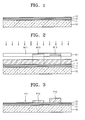
- FIGS. 1 through 16 a flat panel display apparatus according to an embodiment of the present invention will be described.
- FIGS. 1 through 15 are sectional views roughly showing a method of manufacturing an organic light emitting diode (OLED) display apparatus, according to an embodiment of the present invention
- FIG. 16 is a sectional view roughly showing an OLED display apparatus 1 fabricated using the method illustrated in FIGS. 1 through 15 , according to an embodiment of the present invention.
- OLED organic light emitting diode
- the OLED display apparatus 1 includes a substrate 10, a buffer layer 11, a thin-film transistor (TFT) 2, a capacitor 3, and an OLED 4.
- TFT thin-film transistor
- the buffer layer 11, a semiconductor layer 12, and a first conductive layer 13 are sequentially formed on the substrate 10.
- the substrate 10 may be formed of a transparent glass material primarily composed of SiO2. However, aspects of the present invention are not limited thereto, and the substrate 10 may be formed of an opaque glass material, plastics, or other such materials. However, if the OLED display apparatus 1 is a bottom emission type OLED display apparatus in which images of the OLED display apparatus 1 are viewed below the substrate 10, the substrate 10 should be formed of a transparent material.
- the buffer layer 11 may be disposed on the top surface of the substrate 10 to smooth the substrate 10 and to preventing impurities from penetrating into the substrate 10.
- the buffer layer 11 may be formed of SiO2 and/or SiNx, and may be deposited by using a deposition method such as plasma enhanced chemical vapor deposition (PECVD), atmospheric pressure CVD (APCVD), low pressure CVD (LPCVD), or other similar deposition methods.
- PECVD plasma enhanced chemical vapor deposition
- APCVD atmospheric pressure CVD
- LPCVD low pressure CVD
- the semiconductor layer 12 may be formed of poly-crystal silicon crystallized after depositing amorphous silicon.
- the amorphous silicon may be crystallized by rapid thermal annealing (RTA), solid phase crystallization (SPC), excimer laser annealing (ELA), metal induced crystallization (MIC), metal induced lateral crystallization (MILC), sequential lateral solidification (SLS), or the like.
- the first conductive layer 13 is formed on the semiconductor layer 12. According to the present embodiment, the first conductive layer 13 is formed by depositing amorphous silicon containing n-type or p-type impurities and performing a heat treatment process on the amorphous silicon. However, aspects of the present invention are not limited thereto, and the first conductive layer 13 may include any material containing a metal.
- photoresist is applied to the top surface of the structure shown in FIG. 1 , and a first photoresist layer P1 is formed by either pre-baking or soft-baking the photoresist.
- a first mask M1 on which a predetermined pattern is printed is prepared and aligned on the substrate 10 for patterning the first photoresist layer P1.
- the first mask M1 is a half-tone mask including a photo-transmissive region M11, a photo-interceptive region M12, and a semi photo-transmissive region M13.
- the photo-transmissive region M11 transmits light of wavelengths in a predetermined range.
- the photo-interceptive region M12 blocks irradiated light.
- the semi photo-transmissive region M13 transmits only some of the irradiated light.
- FIG. 2 is a concept view describing concepts of each of the regions of the first mask M1.
- the first mask M1 may be formed as a predetermined pattern on a transparent substrate, such as a quartz (Qz) substrate.
- the photo-interceptive region M12 is formed by patterning materials such as Cr or CrO2 on the quartz substrate, and the semi photo-transmissive region M13 may be formed of at least one of Cr, Si, Mo, Ta, and Al. Photo-transmissivity of the semi photo-transmissive region M13 may be controlled by changing composition ratio and/or thickness of materials forming the semi photo-transmissive region M13.
- the first mask M1 on which a pattern as described above is printed is aligned on the substrate 10, and a photolithographic operation is performed by irradiating light of wavelengths in a predetermined range onto the first photoresist layer P1.
- Figure 3 shows a pattern of the first photoresist layer P1 remaining after removing exposed portions of the first photoresist layer P1.
- positive photoresist of which exposed portions are removed, is used in the current embodiment, aspects of the present invention are not limited thereto, and negative photoresist can also be used.
- a portion P11 of the photoresist layer P1 corresponding to the photo-transmissive region M11 of the first mask M1 is removed, whereas a portion P12 of the first photoresist layer P1 corresponding to the photo-interceptive region M12 and a portion P13 of the first photoresist layer P1 corresponding to the semi photo-transmissive region M13 remain.
- the thickness of the portion P13 of the first photoresist layer P1 corresponding to the semi photo-transmissive region M13 is less than that of the portion P12 of the first photoresist layer P1 corresponding to the photo-interceptive region M12, and the thickness of the portion P13 may be controlled by changing the composition ratio and/or thickness of materials forming the semi photo-transmissive region M13.
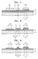
- the semiconductor layer 12 and the first conductive layer 13 on the substrate 10 are etched using etching equipment, wherein the portions P12 and P13 of the first photoresist layer P1 are used as etching masks.
- the region P11 is etched first, and the thickness of the region P13 of the first photoresist layer P1 is reduced by etching.
- the etching operation may comprise wet etching, dry etching, or the like, however, aspects of the present invention are not limited thereto.
- portions of the semiconductor layer 12 and the first conductive layer 13 of FIG. 3 corresponding to the portion P11 of the first photoresist layer P1 are etched. Furthermore, although the portion P13 of the photoresist layer P13 corresponding to the semi photo-transmissive region M13 of FIG. 3 is etched, structures below the portion P13 of the photoresist layer P13 remain. Meanwhile, the portion P12 of the first photoresist layer P1 corresponding to the photo-interceptive region M12 partially remains after the first etching operation, and a second etching operation is performed by using the remainder of the portion P12 of the first photoresist layer P1 as an etching mask.
- the remainder of the portion P12 of the photoresist layer P1, which remained after the first etching operation, and the first conductive layer 13 in the region corresponding to the semi photo-transmissive region M13, are completely etched in the second etching operation.
- a first electrode 31 and an active layer 21 are formed on the buffer layer 11, wherein the first electrode 31 includes a first bottom electrode 31-1 including a portion of the semiconductor layer 12 and a first top electrode 31-2 including a portion of the first conductive layer 13, and the active layer 21 includes a portion of the semiconductor layer 12.
- the first bottom electrode 31-1 and the first top electrode 31-2 constitute a capacitor, and the active layer 21 is part of a TFT
- the active layer 21 of the TFT and the first bottom electrode 31-1 and the first top electrode 31-2 of the capacitor are simultaneously patterned on a same structure by using the same mask M1, and thus the active layer 21 of the TFT and the first bottom electrode 31-1 of the capacitor are formed of the same material and are formed on the same layer. Furthermore, since they are simultaneously patterned by using the same mask M1, shapes of ends of the capacitor formed by the first bottom electrode 31-1 and the first top electrode 31-2 are the same.
- a first insulation layer 14, a second conductive layer 15, and a third conductive layer 16 are sequentially formed on the structure of FIG. 5 , which is the result of the first masking operation.
- a second photoresist layer P2 is formed on the third conductive layer 16, and a second mask M2 is aligned on the substrate 10.
- the first insulation layer 14 may be formed by depositing an inorganic insulation material using a deposition method such as PECVD, APCVD, LPCVD, or the like, wherein the inorganic insulation material comprises a material such as SiNx or SiOx.
- a portion of the first insulation layer 14 is interposed between the active layer 21 and a gate bottom electrode 22-1 of a TFT 2 (to be described later) and functions as a gate insulation layer of the TFT 2, whereas another portion of the first insulation layer 14 is interposed between the first top electrode 31-2 and a second bottom electrode 32-1 of a capacitor 3 (to be described later) and functions as a first dielectric layer.
- the second conductive layer 15 may contain one or more transparent materials such as ITO, IZO, ZnO, and In203. As shown in FIG. 8 , the second conductive layer 15 constitutes a pixel bottom electrode 42-1 of a flat panel display, a gate bottom electrode 22-1 of the TFT 2, and the second bottom electrode 32-1 of the capacitor 3. Although the second conductive layer 15 is formed as a single layer in the current embodiment, aspects of the present invention are not limited thereto, and a plurality of conductive layers may be formed. In other words, when a pixel electrode 42 (to be described later) is only formed of transparent materials as in the current embodiment, the pixel electrode 42 can be used in a bottom-emission type display apparatus in which images are viewed from below the substrate 10.
- a reflective layer may be formed by forming the plurality of second conductive layers and depositing transparent conductive materials thereon, wherein the transparent conductive materials are as materials used in the current embodiment.
- more than two layers may be formed if required, however, aspects of the present invention are not limited thereto.
- the third conductive layer 16 may contain one or more materials from among Ag, Mg, Al, Pt, Pd, Au, Ni, Nd, Ir, Cr, Li, Ca, Mo, Ti, W, MoW, and Al/Cu.
- the third conductive layer 16 constitutes a pixel top electrode 42-2 of a flat panel display, a gate top electrode 22-2 of the TFT 2, and a second top electrode 32-2 of the capacitor 3.
- the second mask M2 includes a photo-transmissive region M21 and photo-interceptive regions M22a, M22b, and M22c in predetermined patterns.
- the second mask M2 is aligned on the substrate 10, and light of wavelengths in a predetermined range is irradiated onto the second photoresist layer P2.
- a portion P21 of the second photoresist layer P2 corresponding to the photo-transmissive region M21 of the second mask M2 is removed, whereas portions P22a, P22b, and P22c of the second photoresist layer P2, which respectively correspond to the photo-interceptive regions M22a, M22b, and M22c, remain.
- the portions P22a, P22b, and P22c of the second photoresist layer P2 are used as masks to etch the second conductive layer 15 and the third conductive layer 16 on the substrate 10 using etching equipment, in a second masking operation.
- the etching operation described above may comprise wet etching, dry etching, or the like, however, aspects of the present invention are not limited thereto.
- FIG. 8 a structure obtained after the etching operation in the second masking operation, is shown. Portions of the second conductive layer 15 and the third conductive layer 16 in the region P21 of the second photoresist layer P2, which is a region from which the second photoresist layer P2 is removed, are etched. In the regions where the second photoresist layer P2 remains, a double-layered gate electrode 22 is patterned to correspond to the center region of the active layer 21 of the TFT 2. Using a pattern of the double-layered gate electrode 22, either n-type or p-type impurities are implanted into edges of the active layer 21 of the TFT 2.
- FIG. 9 shows a structure obtained after etching and ion implanting operations are performed in the second masking operation, is shown.
- the active layer 21 of the TFT 2 includes a source region 21 a, a drain region 21 b, and a channel region 21 c that are formed by the ion implantation.
- the double-layered gate electrode 22, double-layered first and second electrodes 31 and 32 of the capacitor 3, and a double-layered pixel electrode 42 are formed at a location corresponding to the channel region 21 c of the TFT 2.
- the double-layered pixel electrode 42, the gate electrode 21 of the TFT 2, and the second electrode 32 of the capacitor 3 are simultaneously patterned on the same structure using the same second mask M2.
- the pixel bottom electrode 42-1, the gate bottom electrode 21-1 of the TFT 2, and the second bottom electrode 32-1 are formed of the same material and formed on the same layer
- the pixel top electrode 42-2, the gate top electrode 21-2 of the TFT 2, and the second top electrode 32-2of the capacitor 3 are formed of the same material and formed on the same layer.
- shapes of ends of each of the pixel bottom electrode 42-1 and the pixel top electrode 42-2, ends of the gate bottom electrode 22-1 and the gate top electrode 22-2, and ends of the second bottom electrode 32-1 and the second top electrode 32-2 of the capacitor 3 are the same.
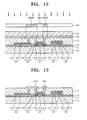
- a second insulation layer 17 is formed on the structure shown in FIG. 9 , which is a result of the second masking operation.
- a third photoresist layer P3 is formed on the second insulation layer 17, and a third mask M3 is aligned on the substrate 10.
- the second insulation layer 17 may be formed of one or more organic insulation materials, such as polyimide, polyamide, acryl resin, and phenol resin, using a method such as spin coating.
- the second insulation 17 is formed to have a thickness sufficient to function as an interlayer insulation layer between the double-layered gate electrode 22 of the thin-film transistor (TFT) 2 and a source electrode 24a and a drain electrode 24b described below.
- the second insulation layer 17 may be formed of not only organic insulation materials as described above, but also inorganic insulation materials as the first insulation layer 14 described above.
- the second insulation layer 17 may also be formed by alternating organic insulation materials and inorganic insulation materials of an alternate structure of organic insulation materials and inorganic insulation materials.
- the third mask M3 is patterned to include photo-transmissive regions M31 a, M31 b, and M31 c and a photo-interceptive region M32, corresponding to portions of the source region 21 a and the drain region 21 b and portions of the edges of the pixel electrode 42.
- the third mask M3 including the patterns described above is aligned on the substrate 10, and a photolithographic operation is performed thereon.
- FIG. 11 illustrates the resulting structure after an etching operation using the remaining portions of the third photoresist layer P3 as etching masks is performed, wherein the remaining portions remain after exposed portions of the third photoresist layer P3 are removed. This is referred to as a third masking operation. Openings 23a, 23b, and 23c, which expose the portions of the source region 21 a and the drain region 21 b and a region corresponding to the portions of the edges of the pixel top electrode 42-2, are formed.
- the openings 23a, 23b, and 23c From among the openings 23a, 23b, and 23c, the openings 23a and 23b formed in the portions of the source region 21 a and the drain region 21 b constitute contact holes, whereas the opening 23c formed in the region corresponding to the portions of the edges of the pixel top electrode 42-2 constitutes a via hole.
- aspects of the present invention are not limited to such names.
- a fourth conductive layer 18 is formed on the structure of FIG. 11 , which is a result of the third masking operation.
- a fourth photoresist layer P4 is formed on the fourth conductive layer 18, and a fourth mask M4 is aligned on the substrate 10.
- the fourth conductive layer 18 may be formed of the material used to form the second conductive layer 15 and/or the third conductive layer 16 described above, aspects of the present invention are not limited thereto, and the fourth conductive layer 18 may be formed of various conductive materials. Furthermore, the conductive materials are deposited to a thickness sufficient to fill the openings 23a, 23b, and 23c described above.
- the fourth mask M4 includes a photo-transmissive region M41 and photo-interceptive regions M42a and M42b. After a photolithographic operation is performed on the fourth photoresist layer P4 and the fourth photoresist layer P4 is developed, remaining portions of the fourth photoresist layer P4 are used as etching masks for an etching operation in a fourth masking operation.
- the source electrode 24a and the drain electrode 24b which respectively contact the source region 21 a and the drain region 21 b via the contact holes 23a and 23b, are formed on the second insulation layer 17. Furthermore, one of the source electrode 24a and the drain electrode 24b is formed to be connected to the pixel top electrode 42-2 via the via hole 23c, wherein the via hole 23c is connected to a portion of the edge regions of the pixel top electrode 42-2.
- a third insulation layer 19 is formed on the structure illustrated in FIG. 13 , which is a result of the fourth masking operation, and a fifth mask M5 is aligned on the substrate 10.
- the third insulation layer 19 may be formed of one or more organic insulation materials, such as polyimide, polyamide, acryl resin, and phenol resin, using a method such as spin coating. Meanwhile, the third insulation layer 19 may be formed of organic insulation materials as described above, and also the inorganic insulation materials used to form the first insulation layer 14 and the second insulation layer 17 described above.
- the third insulation layer 19 functions as a pixel defining layer (PDL) 43 of the OLED apparatus 1 described below, after an etching operation is performed using the fifth mask M5.
- PDL pixel defining layer
- the fifth mask M5 includes a photo-transmissive region M51 formed in a portion thereof corresponding to the double-layered pixel electrode 42 and a photo-interceptive region M52 formed in remaining portions thereof.
- the second insulation layer 17, the third insulation layer 19, and the pixel top electrode 42-2 in a region corresponding to the photo-transmissive region M51 are etched, and thus the pixel bottom electrode 42-1 is exposed.
- the second insulation layer 17 and the third insulation layer 19 are sequentially stacked on the edge of the pixel top electrode 42-2 around an opening 44 formed in the etching operation above.
- the third insulation layer 19, which is formed to have a predetermined thickness along the opening 44 widens an interval between the edge of the double-layered pixel electrode 42 and an opposite electrode 47 described below to prevent concentration of electric field at the edge of the pixel electrode 42.
- the third insulation layer 19 functions as the PDL 43 preventing a short between a pixel electrode 42 and an opposite electrode which is the two-way electrode 47.
- an intermediate layer 46 which includes an organic light emitting layer 45, and the two-way electrode 47 are formed on the exposed portion of the pixel bottom electrode 42-1 and the PDL 43.
- the organic light emitting layer 45 emits light when electrically driven by the double-layered pixel electrode 42 and the two-way electrode 47.
- the organic light emitting layer 45 may be formed of either a low molecular organic material or a high molecular organic material.
- the intermediate layer 46 may include a hole transport layer (HTL) and a hole injection layer (HIL) stacked toward the pixel electrode 42, and an electron transport layer (ETL) and an electron injection layer (ElL) stacked toward the two-way electrode 47.
- HTL hole transport layer
- HIL hole injection layer
- ETL electron transport layer
- ElL electron injection layer
- various other layers may be stacked if required.
- organic materials such as copper phthalocyanine (CuPc), N,N'-Di(naphthalene-1-yl)-N,N'-diphenyl-benzidine, tris-8-hydroxyquinoline aluminum (Alq3), etc., may be used as the organic light emitting layer 45.
- the intermediate layer 46 may include only the HTL formed toward the pixel electrode 42 from the organic light emitting layer 43.
- the HTL may be formed of poly-(2,4)-ethylene-dihydroxy thiophene (PEDOT), polyaniline (PANI), etc., and may be formed on the top surface of the pixel electrode 42 using a method such as inkjet printing or spin coating.
- organic materials may be high molecular organic materials such as a poly-phenylenevinylene material or a polyfluorene material, and a color pattern may be formed by using a general method such as inkjet printing, spin coating, or heat transference using a laser.
- the two-way electrode 47 is formed on the intermediate layer 46 including the organic light emitting layer 45, as a common electrode.
- the pixel electrode 42 is used as an anode electrode
- the two-way electrode 47 that is formed as a common electrode is used as a cathode electrode.
- aspects of the present invention are not limited thereto and the polarity of the pixel electrode 42 and the two-way electrode 47 that is formed as a common electrode may be reversed.
- the pixel electrode 45 becomes a transparent electrode and the two-way electrode 47 that is formed as a common electrode becomes a reflective electrode.
- the reflective electrode may be formed by depositing a thin layer of metal with a small work function, such as Ag, Mg, Al, Pt, Pd, Au, Ni, Nd, Ir, Cr, Li, Ca, LiF/Ca, LiF/Al, or a compound thereof.
- a sealant and a moisture absorbent may further be disposed on the two-way electrode 47 that is formed as a common electrode for protecting the organic light emitting layer 45 from external moisture or oxygen.
- an OLED apparatus can be manufactured by using a small number of masks. Therefore, manufacturing costs can be reduced and the manufacturing process can be simplified due to a reduction in the number of masks required.
- the half-tone mask is used only once, and thus a cost increase due to the use of the half-tone mask can be minimized.
- the pixel electrode is kept protected by the second insulation layer and the third insulation layer, and is exposed right before the organic light emitting layer is formed.
- damage to the pixel electrode can be prevented, as compared to conventional methods of manufacturing OLED apparatuses in which manufacturing operations are performed while pixel electrodes are exposed.
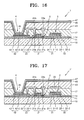
- FIG. 17 is a cross-sectional view of an OLED apparatus 1' according to another embodiment of the present invention.
- the OLED apparatus 1' according to the current embodiment includes the substrate 10, the buffer layer 11, and the TFT 2 of the previous embodiment, a capacitor 3', and an OLED 4.
- the structure of the capacitor 3' in the OLED apparatus 1' according to the current embodiment is different from the structure of the capacitor 3 in the OLED apparatus 1. The description below will focus on this difference.
- the capacitor 3' of the OLED apparatus 1' includes a third electrode 33.
- the third electrode 33 of the capacitor 3' is formed on a portion of the second insulation layer 17 corresponding to the second top electrode 32-2 of the capacitor 3'.
- the third electrode 33 of the capacitor 3' is formed of the material used to form the source electrode and the drain electrode 24a and 24b.
- a photolithographic operation is performed on the portion of the second insulation layer 17 corresponding to the second top electrode 32-2 of the capacitor 3' by using a mask pattern.
- the photo-interceptive region is formed in the portion of the second insulation layer 17 in the fourth masking operation to fabricate the capacitor 3' according to the current embodiment.
- the capacitance of the capacitor 3' of the OLED apparatus 1 increases, and thus the increased capacitance of the capacitor 3' contributes not only to the cost reduction due to reduction of mask usage and pixel electrode damage prevention, but also to display quality of the OLED apparatus 1'.
- FIGS. 18 through 21 are cross-sectional views illustrating another method of manufacturing an OLED apparatus.
- the OLED apparatus 1' includes the substrate 10, the buffer layer 11, the capacitor 3 and the OLED 4 of the embodiment illustrated in FIGS. 1 through 16 , and a TFT 2'.
- the structure of the TFT 2' in the OLED apparatus 1', according to the current embodiment, is different from the structure of the TFT 2 in the OLED apparatus 1. The description below will focus on this difference.
- a first photoresist layer P1' is formed on the structure illustrated in FIG. 1 , and a first mask M1' on which a predetermined pattern is printed is aligned on the substrate 10 to pattern the first photoresist layer P1'.
- the first mask M1' is a half-tone mask including a photo-transmissive region M11', photo-interceptive regions M12a', M12b', and M12c', and a semi photo-transmissive region M13'.
- the first mask M1' including the pattern described above is aligned on the substrate 10, and a photolithographic operation is performed by irradiating light of wavelengths in a predetermined range on the first mask M1'.
- Figure 19 shows a pattern of the first photoresist layer P1' remaining after a developing process is performed, by which exposed portions of the photoresist layer P1' are removed.
- a portion P11' of the first photoresist layer P1' corresponding to the photo-transmissive M11' of the first mask M1' is removed, whereas portions P12a', P12b', and P12c' of the first photoresist layer P1' respectively corresponding to the photo-interceptive regions M12a', M12b', and M12c' and a portion P13' of the first photoresist layer P1' corresponding to the semi photo-transmissive region M13' remain.
- the semiconductor layer 12 and the first conductive layer 13 on the substrate 10 are etched by using etching equipment.
- exposed portions of the semiconductor layer 12 and the first conductive layer 13 from which the first photoresist layer P1' has been removed are etched first, and the thickness of the first photoresist layer P1' is reduced by being etched.
- the etching operation may comprise wet etching, dry etching, or the like.
- portions of the semiconductor layer 12 and the first conductive layer 13, shown in FIG. 19 , in the portion P11 are etched. Furthermore, referring to FIG. 20 , although the portion P13' of the first photoresist layer P1' corresponding to the semi photo-transmissive region M13' is etched, structures below the portion P13' remain. Meanwhile, the portions P12a', P12b', and P12c' of the first photoresist layer P1' respectively corresponding to the photo-interceptive regions M12a, M12b, and M12c partially remain after the first etching operation, and a second etching operation is performed by using them as etching masks.
- FIG. 21 shows a shape of the OLED apparatus 1' after the remaining portions P12a', P12b', and P12c' illustrated in FIG. 20 are completely etched after the second etching operation and then the second through fourth masking operations are completed.
- the source region and the drain region are formed during an etching operation using the first mask M1'.
- a separate ion implanting operation is not necessary, unlike in the previous embodiment of the present invention, and thus the manufacturing process can be simplified.
- FIG. 22 is a cross-sectional view of an OLED apparatus according to yet another embodiment of the present invention.
- the OLED apparatus includes the substrate 10, the buffer layer 11, the TFT 2', the capacitor 3', and the OLED 4. Structures of the TFT 2' and the capacitor 3' in the OLED apparatus, according to the current embodiment, are different from the structures of the TFT 2 and the capacitor 3 in the OLED apparatus 1 according to the embodiment illustrated in FIGS. 1 through 16 .
- the TFT 2' includes the source region 21 a' and the drain region 21 b' that are formed of the material used to form the first top electrode 31-2 of the capacitor 3 during the first masking operation.
- the capacitor 3' further includes the third electrode 33 of the capacitor 3' that is formed of the material used to form the source electrode 24a and the drain electrode 24b during the fourth masking operation.
- the OLED apparatus According to the OLED apparatus according to the current embodiment, a separate ion implanting operation for forming the source region and the drain region is not necessary, and thus the overall manufacturing process is simplified. Furthermore, the capacitance of the capacitor 3' increases, and thus the increased capacitance of the capacitor 3' contributes to the cost reduction due to reduction of mask usage and pixel electrode damage prevention and also to display quality of the OLED apparatus.
- an OLED apparatus is used as an example of a flat panel display apparatus in the embodiments described above, aspects of the present invention are not limited thereto, and various display devices such as a liquid crystal display (LCD) device, etc. can be used.
- LCD liquid crystal display
- FIGS. 1 through 22 Although one TFT and one capacitor are illustrated in FIGS. 1 through 22 for convenience of explanation, aspects of the present invention are not limited thereto. Thus, it is clear that a plurality of TFTs and a plurality of capacitors can be included.
Applications Claiming Priority (1)
| Application Number | Priority Date | Filing Date | Title |
|---|---|---|---|
| KR1020090007385A KR101074788B1 (ko) | 2009-01-30 | 2009-01-30 | 평판 표시 장치 및 이의 제조 방법 |
Publications (3)
| Publication Number | Publication Date |
|---|---|
| EP2214211A2 true EP2214211A2 (de) | 2010-08-04 |
| EP2214211A3 EP2214211A3 (de) | 2013-07-31 |
| EP2214211B1 EP2214211B1 (de) | 2016-09-28 |
Family
ID=42236517
Family Applications (1)
| Application Number | Title | Priority Date | Filing Date |
|---|---|---|---|
| EP10250161.6A Active EP2214211B1 (de) | 2009-01-30 | 2010-01-29 | Flachbildschirmanzeigevorrichtung und Herstellungsverfahren dafür |
Country Status (5)
| Country | Link |
|---|---|
| US (1) | US8106402B2 (de) |
| EP (1) | EP2214211B1 (de) |
| JP (1) | JP5202554B2 (de) |
| KR (1) | KR101074788B1 (de) |
| CN (1) | CN101794049B (de) |
Cited By (5)
| Publication number | Priority date | Publication date | Assignee | Title |
|---|---|---|---|---|
| DE102011005528B4 (de) * | 2010-05-17 | 2013-11-21 | Samsung Display Co., Ltd. | Herstellungsverfahren für eine organische lichtemittierende Anzeigevorrichtung |
| EP2463911A3 (de) * | 2010-12-08 | 2014-01-15 | Samsung Display Co., Ltd. | OLED Anzeigevorrichtung und Verfahren zu deren Herstellung |
| EP2500946A3 (de) * | 2011-03-14 | 2014-03-05 | Samsung Display Co., Ltd. | Organische lichtemittierende Anzeige und Verfahren zu ihrer Herstellung |
| GB2492607B (en) * | 2010-09-20 | 2014-10-22 | Lg Display Co Ltd | Organic light emitting diode display and method for manufacturing the same |
| WO2016170355A1 (en) * | 2015-04-22 | 2016-10-27 | Flexenable Limited | A control component for a current-driven optical media |
Families Citing this family (106)
| Publication number | Priority date | Publication date | Assignee | Title |
|---|---|---|---|---|
| KR20110024531A (ko) * | 2009-09-02 | 2011-03-09 | 삼성모바일디스플레이주식회사 | 유기 발광 디스플레이 장치 |
| KR101084277B1 (ko) * | 2010-02-03 | 2011-11-16 | 삼성모바일디스플레이주식회사 | 유기 발광 표시장치 및 그 제조방법 |
| KR101056429B1 (ko) * | 2010-03-16 | 2011-08-11 | 삼성모바일디스플레이주식회사 | 표시 장치 및 이의 제조 방법 |
| KR101210146B1 (ko) | 2010-04-05 | 2012-12-07 | 삼성디스플레이 주식회사 | 표시 장치 및 그의 제조 방법 |
| KR101234230B1 (ko) * | 2010-06-17 | 2013-02-18 | 삼성디스플레이 주식회사 | 유기 발광 디스플레이 장치 및 그 제조 방법 |
| KR101193197B1 (ko) * | 2010-07-07 | 2012-10-19 | 삼성디스플레이 주식회사 | 유기 발광 표시 장치 및 이의 제조 방법 |
| KR101777246B1 (ko) * | 2010-08-30 | 2017-09-12 | 삼성디스플레이 주식회사 | 유기 발광 디스플레이 장치 및 그 제조 방법 |
| KR101323555B1 (ko) * | 2010-09-20 | 2013-10-29 | 엘지디스플레이 주식회사 | 유기전계발광표시장치 및 그 제조방법 |
| KR101780250B1 (ko) * | 2010-09-24 | 2017-09-22 | 삼성디스플레이 주식회사 | 유기 발광 디스플레이 장치 및 이의 제조 방법 |
| KR101746617B1 (ko) | 2010-09-24 | 2017-06-28 | 삼성디스플레이 주식회사 | 유기 발광 표시 장치 및 그 제조 방법 |
| KR101777247B1 (ko) | 2010-09-29 | 2017-09-12 | 삼성디스플레이 주식회사 | 유기 발광 디스플레이 장치 및 그 제조 방법 |
| KR101372852B1 (ko) | 2010-10-05 | 2014-03-10 | 삼성디스플레이 주식회사 | 유기 발광 표시 장치 및 그 제조 방법 |
| KR20120039946A (ko) * | 2010-10-18 | 2012-04-26 | 삼성모바일디스플레이주식회사 | 유기 발광 표시 장치 및 그 제조 방법 |
| KR101782557B1 (ko) * | 2010-10-25 | 2017-09-28 | 삼성디스플레이 주식회사 | 유기 발광 디스플레이 장치 및 그 제조 방법 |
| KR20120043404A (ko) * | 2010-10-26 | 2012-05-04 | 삼성모바일디스플레이주식회사 | 표시장치 및 이의 제조방법 |
| KR101811702B1 (ko) * | 2010-10-27 | 2017-12-26 | 삼성디스플레이 주식회사 | 유기 발광 디스플레이 장치 및 이의 제조 방법 |
| KR101711191B1 (ko) * | 2010-10-28 | 2017-03-02 | 삼성디스플레이 주식회사 | 유기 발광 표시 장치 및 그 제조방법 |
| US8936965B2 (en) * | 2010-11-26 | 2015-01-20 | Semiconductor Energy Laboratory Co., Ltd. | Semiconductor device and manufacturing method thereof |
| KR101807849B1 (ko) * | 2010-12-08 | 2017-12-12 | 삼성디스플레이 주식회사 | 유기 발광 디스플레이 장치 및 이의 제조 방법 |
| KR101736319B1 (ko) | 2010-12-14 | 2017-05-17 | 삼성디스플레이 주식회사 | 유기 발광 표시 장치 및 그 제조 방법 |
| KR101802860B1 (ko) * | 2010-12-14 | 2017-11-30 | 삼성디스플레이 주식회사 | 유기 발광 표시 장치 및 그 제조 방법 |
| TWI417627B (zh) * | 2010-12-24 | 2013-12-01 | Au Optronics Corp | 畫素結構 |
| KR101839930B1 (ko) | 2010-12-29 | 2018-04-27 | 삼성디스플레이 주식회사 | 유기 발광 표시 장치 및 유기 발광 표시 장치 제조 방법 |
| KR101813492B1 (ko) * | 2011-01-05 | 2018-01-02 | 삼성디스플레이 주식회사 | 유기발광 표시장치 및 그 제조방법 |
| JP5725337B2 (ja) * | 2011-03-24 | 2015-05-27 | ソニー株式会社 | 表示装置、表示装置の製造方法および電子機器 |
| CN102651337A (zh) * | 2011-05-13 | 2012-08-29 | 京东方科技集团股份有限公司 | 一种多晶硅tft阵列基板的制造方法 |
| KR20120126950A (ko) * | 2011-05-13 | 2012-11-21 | 삼성디스플레이 주식회사 | 유기발광표시장치 및 이의 제조방법 |
| KR20120129592A (ko) | 2011-05-20 | 2012-11-28 | 삼성디스플레이 주식회사 | 평판 표시 장치용 백플레인, 이를 포함하는 평판 표시 장치, 및 그 제조 방법 |
| KR101842538B1 (ko) * | 2011-05-26 | 2018-03-28 | 삼성디스플레이 주식회사 | 평판 표시 장치용 백플레인, 이를 포함하는 평판 표시 장치, 및 그 제조 방법 |
| TWI423310B (zh) * | 2011-06-10 | 2014-01-11 | Au Optronics Corp | 畫素結構 |
| KR101904464B1 (ko) * | 2011-06-27 | 2018-10-05 | 삼성디스플레이 주식회사 | 유기 발광 표시 장치 및 유기 발광 표시 장치 제조 방법 |
| KR20130007053A (ko) * | 2011-06-28 | 2013-01-18 | 삼성디스플레이 주식회사 | 유기발광표시장치 및 그 제조방법 |
| KR101815256B1 (ko) | 2011-06-28 | 2018-01-08 | 삼성디스플레이 주식회사 | 유기발광표시장치 및 그 제조방법 |
| KR101893355B1 (ko) * | 2011-06-30 | 2018-10-05 | 삼성디스플레이 주식회사 | 발광 소자 및 이를 포함하는 유기 발광 표시 장치 |
| KR101833235B1 (ko) | 2011-07-14 | 2018-04-16 | 삼성디스플레이 주식회사 | 박막 트랜지스터 어레이 기판, 이를 포함하는 유기 발광 표시 장치 및 그 제조 방법 |
| KR101810047B1 (ko) * | 2011-07-28 | 2017-12-19 | 삼성디스플레이 주식회사 | 유기발광표시장치 및 그 제조방법 |
| KR101801350B1 (ko) | 2011-08-01 | 2017-12-21 | 삼성디스플레이 주식회사 | 박막 트랜지스터 어레이 기판, 이를 포함하는 유기 발광 표시 장치 및 그 제조 방법 |
| KR101944916B1 (ko) | 2011-08-01 | 2019-02-08 | 삼성디스플레이 주식회사 | 박막 트랜지스터 어레이 기판, 이를 포함하는 유기 발광 표시 장치 및 그 제조 방법 |
| KR101925540B1 (ko) | 2011-08-04 | 2019-02-28 | 삼성디스플레이 주식회사 | 박막 트랜지스터 어레이 기판, 이를 포함하는 유기 발광 표시 장치 및 그 제조 방법 |
| KR20130016938A (ko) * | 2011-08-09 | 2013-02-19 | 삼성디스플레이 주식회사 | 유기 발광 표시 장치 및 그 제조 방법 |
| KR101930845B1 (ko) * | 2011-08-09 | 2018-12-20 | 삼성디스플레이 주식회사 | 박막 트랜지스터 어레이 기판, 이를 포함하는 유기 발광 표시 장치 및 그 제조 방법 |
| KR101875774B1 (ko) * | 2011-08-10 | 2018-07-09 | 삼성디스플레이 주식회사 | 유기발광표시장치 및 그 제조 방법 |
| CN102709234B (zh) | 2011-08-19 | 2016-02-17 | 京东方科技集团股份有限公司 | 薄膜晶体管阵列基板及其制造方法和电子器件 |
| KR20130024029A (ko) * | 2011-08-30 | 2013-03-08 | 삼성디스플레이 주식회사 | 유기 발광 표시 장치 및 그 제조 방법 |
| KR101837625B1 (ko) | 2011-11-10 | 2018-03-13 | 삼성디스플레이 주식회사 | 유기 발광 표시 장치 및 그 제조 방법 |
| KR101880720B1 (ko) * | 2011-11-18 | 2018-07-23 | 삼성디스플레이 주식회사 | 박막 트랜지스터 어레이 기판, 이를 포함하는 유기 발광 표시 장치 및 그 제조 방법 |
| KR101880723B1 (ko) * | 2011-12-09 | 2018-07-23 | 삼성디스플레이 주식회사 | 유기 발광 표시 장치 |
| KR101901832B1 (ko) * | 2011-12-14 | 2018-09-28 | 삼성디스플레이 주식회사 | 유기 발광 표시 장치 및 유기 발광 표시 장치의 제조 방법 |
| KR101884738B1 (ko) * | 2011-12-23 | 2018-08-31 | 삼성디스플레이 주식회사 | 유기 발광 표시 장치 및 유기 발광 표시 장치의 제조방법 |
| KR20130100629A (ko) * | 2012-03-02 | 2013-09-11 | 삼성디스플레이 주식회사 | 유기 발광 디스플레이 장치 |
| KR101924078B1 (ko) | 2012-03-30 | 2018-12-03 | 삼성디스플레이 주식회사 | 유기 발광 표시 장치 및 유기 발광 표시 장치의 리페어 방법 |
| KR101904466B1 (ko) * | 2012-05-08 | 2018-12-03 | 삼성디스플레이 주식회사 | 유기 발광 표시 장치 및 그 제조방법 |
| KR20140020565A (ko) * | 2012-08-09 | 2014-02-19 | 삼성디스플레이 주식회사 | 유기 발광 표시 장치 및 유기 발광 표시 장치의 제조방법 |
| US8766245B2 (en) * | 2012-08-14 | 2014-07-01 | Guardian Industries Corp. | Organic light emitting diode with transparent electrode and method of making same |
| KR101954978B1 (ko) | 2012-09-06 | 2019-03-08 | 삼성디스플레이 주식회사 | 유기 발광 표시 장치 및 유기 발광 표시 장치 제조 방법 |
| KR101901330B1 (ko) * | 2012-09-19 | 2018-09-27 | 삼성디스플레이 주식회사 | 유기전계발광 표시장치의 제조 방법 |
| CN102842587B (zh) * | 2012-09-24 | 2016-11-16 | 京东方科技集团股份有限公司 | 阵列基板及其制作方法、显示装置 |
| CN102881571B (zh) * | 2012-09-28 | 2014-11-26 | 京东方科技集团股份有限公司 | 有源层离子注入方法及薄膜晶体管有源层离子注入方法 |
| KR102021028B1 (ko) * | 2012-12-04 | 2019-09-16 | 삼성디스플레이 주식회사 | 유기 발광 표시 장치 |
| KR20140081314A (ko) * | 2012-12-21 | 2014-07-01 | 삼성디스플레이 주식회사 | 발광 표시 장치 및 그 제조 방법 |
| KR102015873B1 (ko) * | 2013-01-03 | 2019-10-22 | 삼성디스플레이 주식회사 | 표시장치용 백플레인 및 그의 제조 방법 |
| KR101634135B1 (ko) * | 2013-05-21 | 2016-06-29 | 삼성디스플레이 주식회사 | 발광 소자 및 그 제조방법 |
| KR102116493B1 (ko) * | 2013-05-23 | 2020-06-08 | 삼성디스플레이 주식회사 | 유기발광표시장치 및 이의 제조방법 |
| KR102124044B1 (ko) | 2013-05-23 | 2020-06-18 | 삼성디스플레이 주식회사 | 박막 트랜지스터 기판, 그 제조방법 및 이를 포함하는 유기 발광 디스플레이 장치 |
| KR102075529B1 (ko) | 2013-05-29 | 2020-02-11 | 삼성디스플레이 주식회사 | 평판 표시 장치 및 이의 제조 방법 |
| KR102077144B1 (ko) * | 2013-05-30 | 2020-02-14 | 삼성디스플레이 주식회사 | 유기발광표시장치 및 그 제조 방법 |
| KR102077143B1 (ko) * | 2013-05-30 | 2020-02-14 | 삼성디스플레이 주식회사 | 유기 발광 표시 장치 및 그 제조 방법 |
| KR20150011472A (ko) * | 2013-07-23 | 2015-02-02 | 삼성디스플레이 주식회사 | 박막 트랜지스터 및 그 제조 방법 |
| KR20150012503A (ko) * | 2013-07-25 | 2015-02-04 | 삼성디스플레이 주식회사 | 유기 발광 표시 장치 및 그 제조방법 |
| KR102110226B1 (ko) * | 2013-09-11 | 2020-05-14 | 삼성디스플레이 주식회사 | 표시패널 및 그 제조방법 |
| KR102188029B1 (ko) * | 2013-09-24 | 2020-12-08 | 삼성디스플레이 주식회사 | 유기 발광 표시 장치 및 유기 발광 장치의 제조 방법 |
| CN103489882A (zh) * | 2013-10-17 | 2014-01-01 | 京东方科技集团股份有限公司 | 一种阵列基板及其制备方法、显示装置 |
| CN103715135B (zh) * | 2013-12-16 | 2016-04-06 | 京东方科技集团股份有限公司 | 一种过孔及其制作方法、阵列基板 |
| CN103700707B (zh) | 2013-12-18 | 2018-12-11 | 京东方科技集团股份有限公司 | 薄膜晶体管、阵列基板及其制备方法、显示装置 |
| CN104752464B (zh) * | 2013-12-27 | 2018-08-07 | 昆山国显光电有限公司 | 一种有机发光显示装置及其制备方法 |
| KR20150137214A (ko) * | 2014-05-28 | 2015-12-09 | 삼성디스플레이 주식회사 | 유기발광 디스플레이 장치 및 그 제조방법 |
| CN104157613B (zh) * | 2014-07-31 | 2017-03-08 | 京东方科技集团股份有限公司 | 一种阵列基板的制备方法 |
| KR102393369B1 (ko) * | 2014-10-14 | 2022-05-03 | 삼성디스플레이 주식회사 | 유기 발광 표시 장치 및 그 제조 방법 |
| KR102346675B1 (ko) * | 2014-10-31 | 2022-01-04 | 삼성디스플레이 주식회사 | 디스플레이 장치 및 그 제조 방법 |
| US10381335B2 (en) | 2014-10-31 | 2019-08-13 | ehux, Inc. | Hybrid display using inorganic micro light emitting diodes (uLEDs) and organic LEDs (OLEDs) |
| CN104733323B (zh) * | 2014-12-16 | 2018-04-13 | 深圳市华星光电技术有限公司 | 一种低温多晶硅薄膜晶体管的制造方法 |
| KR102322763B1 (ko) * | 2014-12-19 | 2021-11-08 | 삼성디스플레이 주식회사 | 유기발광 디스플레이 장치 및 그 제조방법 |
| KR20160081101A (ko) | 2014-12-30 | 2016-07-08 | 삼성디스플레이 주식회사 | 유기 발광 표시 장치의 제조 방법 및 상기 제조 방법에 의해 제조된 유기 발광 표시 장치 |
| KR102339284B1 (ko) * | 2014-12-30 | 2021-12-15 | 삼성디스플레이 주식회사 | 유기 발광 표시 장치의 제조 방법 및 상기 제조 방법에 의해 제조된 유기 발광 표시 장치 |
| CN104538357B (zh) | 2015-01-13 | 2018-05-01 | 合肥京东方光电科技有限公司 | 制作阵列基板的方法和阵列基板 |
| TWI549265B (zh) * | 2015-02-11 | 2016-09-11 | 友達光電股份有限公司 | 畫素結構及其製造方法 |
| TWI686870B (zh) * | 2015-03-03 | 2020-03-01 | 日商半導體能源研究所股份有限公司 | 半導體裝置、顯示裝置及使用該顯示裝置之電子裝置 |
| KR102478471B1 (ko) * | 2015-07-03 | 2022-12-19 | 삼성디스플레이 주식회사 | 표시 장치 |
| CN105140240B (zh) * | 2015-08-21 | 2020-01-03 | 京东方科技集团股份有限公司 | 柔性基板及其制作方法、显示装置 |
| CN105355631A (zh) * | 2015-10-10 | 2016-02-24 | 京东方科技集团股份有限公司 | 阵列基板及其制作方法、显示装置、掩膜板 |
| KR102457596B1 (ko) * | 2015-11-02 | 2022-10-21 | 삼성디스플레이 주식회사 | 발광 표시 장치의 제조 방법 |
| CN105914229B (zh) * | 2016-06-24 | 2017-12-15 | 京东方科技集团股份有限公司 | 一种amoled显示基板及其制作方法、显示装置 |
| CN106125432A (zh) | 2016-08-29 | 2016-11-16 | 武汉华星光电技术有限公司 | 显示器及其显示面板 |
| KR20180071538A (ko) * | 2016-12-20 | 2018-06-28 | 엘지디스플레이 주식회사 | 표시 장치용 기판과 그를 포함하는 표시 장치 |
| KR20180099974A (ko) | 2017-02-27 | 2018-09-06 | 삼성디스플레이 주식회사 | 반도체 장치 |
| CN109427243A (zh) * | 2017-08-22 | 2019-03-05 | 上海和辉光电有限公司 | 一种显示面板、装置及制作方法 |
| CN107887398B (zh) * | 2017-11-14 | 2022-01-21 | 京东方科技集团股份有限公司 | 阵列基板及其制备方法、显示面板以及显示装置 |
| CN108831916B (zh) * | 2018-06-25 | 2020-06-05 | 京东方科技集团股份有限公司 | 显示基板及其制备方法、显示装置 |
| CN108899327B (zh) * | 2018-06-29 | 2021-01-26 | 武汉华星光电技术有限公司 | 一种阵列基板及其制备方法、显示器 |
| CN112735325B (zh) * | 2018-10-31 | 2022-05-17 | 武汉天马微电子有限公司 | 一种显示面板和显示装置 |
| CN109659445A (zh) * | 2018-12-19 | 2019-04-19 | 武汉华星光电半导体显示技术有限公司 | 显示面板及其显示屏 |
| CN109659348B (zh) * | 2018-12-20 | 2020-04-03 | 深圳市华星光电半导体显示技术有限公司 | 有机发光器件及其制作方法 |
| WO2020212777A1 (en) | 2019-04-18 | 2020-10-22 | 3M Innovative Properties Company | Organic light emitting diode display with color-correction component |
| KR20220062291A (ko) | 2019-09-18 | 2022-05-16 | 쓰리엠 이노베이티브 프로퍼티즈 캄파니 | 나노구조화된 표면 및 폐쇄된 공극을 포함하는 물품, 및 그의 제조 방법 |
| CN111081737A (zh) * | 2019-12-05 | 2020-04-28 | 深圳市华星光电半导体显示技术有限公司 | 一种阵列基板制备方法及阵列基板 |
| KR20210153808A (ko) | 2020-06-10 | 2021-12-20 | 삼성디스플레이 주식회사 | 디스플레이 장치 및 그 제조방법 |
Family Cites Families (16)
| Publication number | Priority date | Publication date | Assignee | Title |
|---|---|---|---|---|
| KR100892945B1 (ko) * | 2002-02-22 | 2009-04-09 | 삼성전자주식회사 | 액티브 매트릭스형 유기전계발광 표시장치 및 그 제조방법 |
| JP5105690B2 (ja) * | 2002-03-26 | 2012-12-26 | 株式会社半導体エネルギー研究所 | 半導体装置の作製方法 |
| US6853052B2 (en) * | 2002-03-26 | 2005-02-08 | Semiconductor Energy Laboratory Co., Ltd. | Semiconductor device having a buffer layer against stress |
| KR100579182B1 (ko) | 2002-10-30 | 2006-05-11 | 삼성에스디아이 주식회사 | 유기 전계 발광 표시 장치의 제조 방법 |
| CN100385475C (zh) * | 2002-12-27 | 2008-04-30 | 株式会社半导体能源研究所 | 显示装置和电子机器 |
| KR101056013B1 (ko) * | 2004-08-03 | 2011-08-10 | 엘지디스플레이 주식회사 | 액정표시장치용 어레이기판 제조방법 |
| KR100689316B1 (ko) * | 2004-10-29 | 2007-03-08 | 엘지.필립스 엘시디 주식회사 | 유기전계발광다이오드소자 및 그 제조방법 |
| KR101107252B1 (ko) * | 2004-12-31 | 2012-01-19 | 엘지디스플레이 주식회사 | 일렉트로-루미네센스 표시 패널의 박막 트랜지스터 기판및 그 제조 방법 |
| US7410842B2 (en) * | 2005-04-19 | 2008-08-12 | Lg. Display Co., Ltd | Method for fabricating thin film transistor of liquid crystal display device |
| KR20070049742A (ko) * | 2005-11-09 | 2007-05-14 | 엘지.필립스 엘시디 주식회사 | 액정표시장치용 어레이기판과 그 제조방법 |
| JP5060738B2 (ja) * | 2006-04-28 | 2012-10-31 | 株式会社ジャパンディスプレイイースト | 画像表示装置 |
| KR20070112954A (ko) * | 2006-05-24 | 2007-11-28 | 엘지.필립스 엘시디 주식회사 | Tft 어레이 기판 및 그 제조방법 |
| KR100847661B1 (ko) * | 2007-03-21 | 2008-07-21 | 삼성에스디아이 주식회사 | 반도체 장치의 제조 방법 |
| KR100846985B1 (ko) * | 2007-04-06 | 2008-07-17 | 삼성에스디아이 주식회사 | 유기 전계 발광 표시 장치 및 그 제조 방법 |
| JP2008270241A (ja) * | 2007-04-16 | 2008-11-06 | Mitsubishi Electric Corp | アクティブマトリクス表示装置及びその製造方法 |
| KR100964227B1 (ko) * | 2008-05-06 | 2010-06-17 | 삼성모바일디스플레이주식회사 | 평판 표시 장치용 박막 트랜지스터 어레이 기판, 이를포함하는 유기 발광 표시 장치, 및 이들의 제조 방법 |
-
2009
- 2009-01-30 KR KR1020090007385A patent/KR101074788B1/ko active IP Right Grant
- 2009-12-24 US US12/647,055 patent/US8106402B2/en active Active
-
2010
- 2010-01-28 JP JP2010016930A patent/JP5202554B2/ja active Active
- 2010-01-29 EP EP10250161.6A patent/EP2214211B1/de active Active
- 2010-01-29 CN CN201010108451.9A patent/CN101794049B/zh active Active
Non-Patent Citations (1)
| Title |
|---|
| None |
Cited By (8)
| Publication number | Priority date | Publication date | Assignee | Title |
|---|---|---|---|---|
| DE102011005528B4 (de) * | 2010-05-17 | 2013-11-21 | Samsung Display Co., Ltd. | Herstellungsverfahren für eine organische lichtemittierende Anzeigevorrichtung |
| US9029900B2 (en) | 2010-05-17 | 2015-05-12 | Samsung Display Co., Ltd. | Organic light-emitting display device and method of manufacturing the same |
| GB2492607B (en) * | 2010-09-20 | 2014-10-22 | Lg Display Co Ltd | Organic light emitting diode display and method for manufacturing the same |
| EP2463911A3 (de) * | 2010-12-08 | 2014-01-15 | Samsung Display Co., Ltd. | OLED Anzeigevorrichtung und Verfahren zu deren Herstellung |
| EP2500946A3 (de) * | 2011-03-14 | 2014-03-05 | Samsung Display Co., Ltd. | Organische lichtemittierende Anzeige und Verfahren zu ihrer Herstellung |
| US8901563B2 (en) | 2011-03-14 | 2014-12-02 | Samsung Display Co., Ltd. | Organic light-emitting display device and method of manufacturing the same |
| WO2016170355A1 (en) * | 2015-04-22 | 2016-10-27 | Flexenable Limited | A control component for a current-driven optical media |
| US10971062B2 (en) | 2015-04-22 | 2021-04-06 | Flexenable Limited | Control component for a current-driven optical media |
Also Published As
| Publication number | Publication date |
|---|---|
| US8106402B2 (en) | 2012-01-31 |
| CN101794049A (zh) | 2010-08-04 |
| US20100193790A1 (en) | 2010-08-05 |
| KR101074788B1 (ko) | 2011-10-20 |
| EP2214211B1 (de) | 2016-09-28 |
| CN101794049B (zh) | 2015-05-20 |
| JP5202554B2 (ja) | 2013-06-05 |
| EP2214211A3 (de) | 2013-07-31 |
| KR20100088269A (ko) | 2010-08-09 |
| JP2010177668A (ja) | 2010-08-12 |
Similar Documents
| Publication | Publication Date | Title |
|---|---|---|
| EP2214211B1 (de) | Flachbildschirmanzeigevorrichtung und Herstellungsverfahren dafür | |
| KR100943187B1 (ko) | 유기 발광 표시 장치 및 이의 제조 방법 | |
| KR101117725B1 (ko) | 유기 발광 표시 장치 및 이의 제조 방법 | |
| EP2117043B1 (de) | Herstellungsverfahren für eine Anordnung von Dünnschichttransistoren in Form eines Arrays und für eine organische Licht emittierende Anzeigevorrichtung die diese Anordnung umfasst | |
| KR101193197B1 (ko) | 유기 발광 표시 장치 및 이의 제조 방법 | |
| KR101889918B1 (ko) | 유기 발광 디스플레이 장치 및 이의 제조 방법 | |
| US8698147B2 (en) | Organic light emitting display device comprising a metal diffusion medium layer and method of manufacturing the same | |
| US8698146B2 (en) | Organic light emitting display device and method of manufacturing the same | |
| US8445915B2 (en) | Organic light-emitting display device and method of manufacturing the same | |
| US8237156B2 (en) | Organic light emitting display device and method of manufacturing the same | |
| KR20120044019A (ko) | 유기 발광 디스플레이 장치 및 이의 제조 방법 | |
| KR102015873B1 (ko) | 표시장치용 백플레인 및 그의 제조 방법 | |
| KR101117728B1 (ko) | 유기 발광 디스플레이 장치 및 그 제조 방법 | |
| KR20110103904A (ko) | 평판 표시 장치 및 이의 제조 방법 |
Legal Events
| Date | Code | Title | Description |
|---|---|---|---|
| PUAI | Public reference made under article 153(3) epc to a published international application that has entered the european phase |
Free format text: ORIGINAL CODE: 0009012 |
|
| 17P | Request for examination filed |
Effective date: 20100204 |
|
| AK | Designated contracting states |
Kind code of ref document: A2 Designated state(s): AT BE BG CH CY CZ DE DK EE ES FI FR GB GR HR HU IE IS IT LI LT LU LV MC MK MT NL NO PL PT RO SE SI SK SM TR |
|
| AX | Request for extension of the european patent |
Extension state: AL BA RS |
|
| RAP1 | Party data changed (applicant data changed or rights of an application transferred) |
Owner name: SAMSUNG DISPLAY CO., LTD. |
|
| PUAL | Search report despatched |
Free format text: ORIGINAL CODE: 0009013 |
|
| AK | Designated contracting states |
Kind code of ref document: A3 Designated state(s): AT BE BG CH CY CZ DE DK EE ES FI FR GB GR HR HU IE IS IT LI LT LU LV MC MK MT NL NO PL PT RO SE SI SK SM TR |
|
| AX | Request for extension of the european patent |
Extension state: AL BA RS |
|
| RIC1 | Information provided on ipc code assigned before grant |
Ipc: H01L 51/56 20060101ALI20130624BHEP Ipc: H01L 27/32 20060101AFI20130624BHEP |
|
| RBV | Designated contracting states (corrected) |
Designated state(s): AT BE BG CH CY CZ DE DK EE ES FI FR GB GR HR HU IE IS IT LI LT LU LV MC MK MT NL NO PL PT RO SE SI SK SM TR |
|
| RAP1 | Party data changed (applicant data changed or rights of an application transferred) |
Owner name: SAMSUNG DISPLAY CO., LTD. |
|
| GRAP | Despatch of communication of intention to grant a patent |
Free format text: ORIGINAL CODE: EPIDOSNIGR1 |
|
| RIC1 | Information provided on ipc code assigned before grant |
Ipc: H01L 27/32 20060101AFI20160317BHEP Ipc: H01L 51/52 20060101ALI20160317BHEP Ipc: H01L 29/49 20060101ALI20160317BHEP Ipc: H01L 51/56 20060101ALI20160317BHEP Ipc: H01L 27/12 20060101ALI20160317BHEP |
|
| INTG | Intention to grant announced |
Effective date: 20160412 |
|
| GRAS | Grant fee paid |
Free format text: ORIGINAL CODE: EPIDOSNIGR3 |
|
| GRAA | (expected) grant |
Free format text: ORIGINAL CODE: 0009210 |
|
| AK | Designated contracting states |
Kind code of ref document: B1 Designated state(s): AT BE BG CH CY CZ DE DK EE ES FI FR GB GR HR HU IE IS IT LI LT LU LV MC MK MT NL NO PL PT RO SE SI SK SM TR |
|
| REG | Reference to a national code |
Ref country code: GB Ref legal event code: FG4D |
|
| REG | Reference to a national code |
Ref country code: CH Ref legal event code: EP |
|
| REG | Reference to a national code |
Ref country code: AT Ref legal event code: REF Ref document number: 833399 Country of ref document: AT Kind code of ref document: T Effective date: 20161015 |
|
| REG | Reference to a national code |
Ref country code: IE Ref legal event code: FG4D |
|
| REG | Reference to a national code |
Ref country code: DE Ref legal event code: R096 Ref document number: 602010036722 Country of ref document: DE |
|
| REG | Reference to a national code |
Ref country code: FR Ref legal event code: PLFP Year of fee payment: 8 |
|
| REG | Reference to a national code |
Ref country code: LT Ref legal event code: MG4D |
|
| PG25 | Lapsed in a contracting state [announced via postgrant information from national office to epo] |
Ref country code: LT Free format text: LAPSE BECAUSE OF FAILURE TO SUBMIT A TRANSLATION OF THE DESCRIPTION OR TO PAY THE FEE WITHIN THE PRESCRIBED TIME-LIMIT Effective date: 20160928 Ref country code: FI Free format text: LAPSE BECAUSE OF FAILURE TO SUBMIT A TRANSLATION OF THE DESCRIPTION OR TO PAY THE FEE WITHIN THE PRESCRIBED TIME-LIMIT Effective date: 20160928 Ref country code: NO Free format text: LAPSE BECAUSE OF FAILURE TO SUBMIT A TRANSLATION OF THE DESCRIPTION OR TO PAY THE FEE WITHIN THE PRESCRIBED TIME-LIMIT Effective date: 20161228 Ref country code: HR Free format text: LAPSE BECAUSE OF FAILURE TO SUBMIT A TRANSLATION OF THE DESCRIPTION OR TO PAY THE FEE WITHIN THE PRESCRIBED TIME-LIMIT Effective date: 20160928 |
|
| REG | Reference to a national code |
Ref country code: NL Ref legal event code: MP Effective date: 20160928 |
|
| REG | Reference to a national code |
Ref country code: AT Ref legal event code: MK05 Ref document number: 833399 Country of ref document: AT Kind code of ref document: T Effective date: 20160928 |
|
| PG25 | Lapsed in a contracting state [announced via postgrant information from national office to epo] |
Ref country code: GR Free format text: LAPSE BECAUSE OF FAILURE TO SUBMIT A TRANSLATION OF THE DESCRIPTION OR TO PAY THE FEE WITHIN THE PRESCRIBED TIME-LIMIT Effective date: 20161229 Ref country code: LV Free format text: LAPSE BECAUSE OF FAILURE TO SUBMIT A TRANSLATION OF THE DESCRIPTION OR TO PAY THE FEE WITHIN THE PRESCRIBED TIME-LIMIT Effective date: 20160928 Ref country code: NL Free format text: LAPSE BECAUSE OF FAILURE TO SUBMIT A TRANSLATION OF THE DESCRIPTION OR TO PAY THE FEE WITHIN THE PRESCRIBED TIME-LIMIT Effective date: 20160928 Ref country code: SE Free format text: LAPSE BECAUSE OF FAILURE TO SUBMIT A TRANSLATION OF THE DESCRIPTION OR TO PAY THE FEE WITHIN THE PRESCRIBED TIME-LIMIT Effective date: 20160928 |
|
| PG25 | Lapsed in a contracting state [announced via postgrant information from national office to epo] |
Ref country code: EE Free format text: LAPSE BECAUSE OF FAILURE TO SUBMIT A TRANSLATION OF THE DESCRIPTION OR TO PAY THE FEE WITHIN THE PRESCRIBED TIME-LIMIT Effective date: 20160928 Ref country code: RO Free format text: LAPSE BECAUSE OF FAILURE TO SUBMIT A TRANSLATION OF THE DESCRIPTION OR TO PAY THE FEE WITHIN THE PRESCRIBED TIME-LIMIT Effective date: 20160928 |
|
| PG25 | Lapsed in a contracting state [announced via postgrant information from national office to epo] |
Ref country code: ES Free format text: LAPSE BECAUSE OF FAILURE TO SUBMIT A TRANSLATION OF THE DESCRIPTION OR TO PAY THE FEE WITHIN THE PRESCRIBED TIME-LIMIT Effective date: 20160928 Ref country code: CZ Free format text: LAPSE BECAUSE OF FAILURE TO SUBMIT A TRANSLATION OF THE DESCRIPTION OR TO PAY THE FEE WITHIN THE PRESCRIBED TIME-LIMIT Effective date: 20160928 Ref country code: BG Free format text: LAPSE BECAUSE OF FAILURE TO SUBMIT A TRANSLATION OF THE DESCRIPTION OR TO PAY THE FEE WITHIN THE PRESCRIBED TIME-LIMIT Effective date: 20161228 Ref country code: SK Free format text: LAPSE BECAUSE OF FAILURE TO SUBMIT A TRANSLATION OF THE DESCRIPTION OR TO PAY THE FEE WITHIN THE PRESCRIBED TIME-LIMIT Effective date: 20160928 Ref country code: PL Free format text: LAPSE BECAUSE OF FAILURE TO SUBMIT A TRANSLATION OF THE DESCRIPTION OR TO PAY THE FEE WITHIN THE PRESCRIBED TIME-LIMIT Effective date: 20160928 Ref country code: BE Free format text: LAPSE BECAUSE OF FAILURE TO SUBMIT A TRANSLATION OF THE DESCRIPTION OR TO PAY THE FEE WITHIN THE PRESCRIBED TIME-LIMIT Effective date: 20160928 Ref country code: AT Free format text: LAPSE BECAUSE OF FAILURE TO SUBMIT A TRANSLATION OF THE DESCRIPTION OR TO PAY THE FEE WITHIN THE PRESCRIBED TIME-LIMIT Effective date: 20160928 Ref country code: IS Free format text: LAPSE BECAUSE OF FAILURE TO SUBMIT A TRANSLATION OF THE DESCRIPTION OR TO PAY THE FEE WITHIN THE PRESCRIBED TIME-LIMIT Effective date: 20170128 Ref country code: SM Free format text: LAPSE BECAUSE OF FAILURE TO SUBMIT A TRANSLATION OF THE DESCRIPTION OR TO PAY THE FEE WITHIN THE PRESCRIBED TIME-LIMIT Effective date: 20160928 Ref country code: PT Free format text: LAPSE BECAUSE OF FAILURE TO SUBMIT A TRANSLATION OF THE DESCRIPTION OR TO PAY THE FEE WITHIN THE PRESCRIBED TIME-LIMIT Effective date: 20170130 |
|
| REG | Reference to a national code |
Ref country code: DE Ref legal event code: R097 Ref document number: 602010036722 Country of ref document: DE |
|
| PG25 | Lapsed in a contracting state [announced via postgrant information from national office to epo] |
Ref country code: IT Free format text: LAPSE BECAUSE OF FAILURE TO SUBMIT A TRANSLATION OF THE DESCRIPTION OR TO PAY THE FEE WITHIN THE PRESCRIBED TIME-LIMIT Effective date: 20160928 |
|
| PG25 | Lapsed in a contracting state [announced via postgrant information from national office to epo] |
Ref country code: DK Free format text: LAPSE BECAUSE OF FAILURE TO SUBMIT A TRANSLATION OF THE DESCRIPTION OR TO PAY THE FEE WITHIN THE PRESCRIBED TIME-LIMIT Effective date: 20160928 |
|
| PLBE | No opposition filed within time limit |
Free format text: ORIGINAL CODE: 0009261 |
|
| STAA | Information on the status of an ep patent application or granted ep patent |
Free format text: STATUS: NO OPPOSITION FILED WITHIN TIME LIMIT |
|
| REG | Reference to a national code |
Ref country code: CH Ref legal event code: PL |
|
| 26N | No opposition filed |
Effective date: 20170629 |
|
| PG25 | Lapsed in a contracting state [announced via postgrant information from national office to epo] |
Ref country code: MC Free format text: LAPSE BECAUSE OF FAILURE TO SUBMIT A TRANSLATION OF THE DESCRIPTION OR TO PAY THE FEE WITHIN THE PRESCRIBED TIME-LIMIT Effective date: 20160928 |
|
| PG25 | Lapsed in a contracting state [announced via postgrant information from national office to epo] |
Ref country code: LI Free format text: LAPSE BECAUSE OF NON-PAYMENT OF DUE FEES Effective date: 20170131 Ref country code: CH Free format text: LAPSE BECAUSE OF NON-PAYMENT OF DUE FEES Effective date: 20170131 |
|
| REG | Reference to a national code |
Ref country code: IE Ref legal event code: MM4A |
|
| PG25 | Lapsed in a contracting state [announced via postgrant information from national office to epo] |
Ref country code: SI Free format text: LAPSE BECAUSE OF FAILURE TO SUBMIT A TRANSLATION OF THE DESCRIPTION OR TO PAY THE FEE WITHIN THE PRESCRIBED TIME-LIMIT Effective date: 20160928 Ref country code: LU Free format text: LAPSE BECAUSE OF NON-PAYMENT OF DUE FEES Effective date: 20170129 |
|
| REG | Reference to a national code |
Ref country code: FR Ref legal event code: PLFP Year of fee payment: 9 |
|
| PG25 | Lapsed in a contracting state [announced via postgrant information from national office to epo] |
Ref country code: IE Free format text: LAPSE BECAUSE OF NON-PAYMENT OF DUE FEES Effective date: 20170129 |
|
| PG25 | Lapsed in a contracting state [announced via postgrant information from national office to epo] |
Ref country code: MT Free format text: LAPSE BECAUSE OF NON-PAYMENT OF DUE FEES Effective date: 20170129 |
|
| PG25 | Lapsed in a contracting state [announced via postgrant information from national office to epo] |
Ref country code: HU Free format text: LAPSE BECAUSE OF FAILURE TO SUBMIT A TRANSLATION OF THE DESCRIPTION OR TO PAY THE FEE WITHIN THE PRESCRIBED TIME-LIMIT; INVALID AB INITIO Effective date: 20100129 |
|
| PG25 | Lapsed in a contracting state [announced via postgrant information from national office to epo] |
Ref country code: CY Free format text: LAPSE BECAUSE OF NON-PAYMENT OF DUE FEES Effective date: 20160928 |
|
| PG25 | Lapsed in a contracting state [announced via postgrant information from national office to epo] |
Ref country code: MK Free format text: LAPSE BECAUSE OF FAILURE TO SUBMIT A TRANSLATION OF THE DESCRIPTION OR TO PAY THE FEE WITHIN THE PRESCRIBED TIME-LIMIT Effective date: 20160928 |
|
| PG25 | Lapsed in a contracting state [announced via postgrant information from national office to epo] |
Ref country code: TR Free format text: LAPSE BECAUSE OF FAILURE TO SUBMIT A TRANSLATION OF THE DESCRIPTION OR TO PAY THE FEE WITHIN THE PRESCRIBED TIME-LIMIT Effective date: 20160928 |
|
| REG | Reference to a national code |
Ref country code: DE Ref legal event code: R079 Ref document number: 602010036722 Country of ref document: DE Free format text: PREVIOUS MAIN CLASS: H01L0027320000 Ipc: H10K0059000000 |
|
| P01 | Opt-out of the competence of the unified patent court (upc) registered |
Effective date: 20230515 |
|
| PGFP | Annual fee paid to national office [announced via postgrant information from national office to epo] |
Ref country code: GB Payment date: 20231220 Year of fee payment: 15 |
|
| PGFP | Annual fee paid to national office [announced via postgrant information from national office to epo] |
Ref country code: FR Payment date: 20231222 Year of fee payment: 15 |
|
| PGFP | Annual fee paid to national office [announced via postgrant information from national office to epo] |
Ref country code: DE Payment date: 20231220 Year of fee payment: 15 |