EP2169459B1 - Image sensing apparatus, image sensing system and focus detection method - Google Patents
Image sensing apparatus, image sensing system and focus detection method Download PDFInfo
- Publication number
- EP2169459B1 EP2169459B1 EP09168519.8A EP09168519A EP2169459B1 EP 2169459 B1 EP2169459 B1 EP 2169459B1 EP 09168519 A EP09168519 A EP 09168519A EP 2169459 B1 EP2169459 B1 EP 2169459B1
- Authority
- EP
- European Patent Office
- Prior art keywords
- focus detection
- image
- exit pupil
- image sensor
- pixels
- Prior art date
- Legal status (The legal status is an assumption and is not a legal conclusion. Google has not performed a legal analysis and makes no representation as to the accuracy of the status listed.)
- Not-in-force
Links
- 238000001514 detection method Methods 0.000 title claims description 200
- 210000001747 pupil Anatomy 0.000 claims description 138
- 238000000034 method Methods 0.000 claims description 34
- 238000012937 correction Methods 0.000 claims description 16
- 238000006243 chemical reaction Methods 0.000 claims description 15
- 230000003287 optical effect Effects 0.000 description 43
- 238000010586 diagram Methods 0.000 description 42
- 238000004519 manufacturing process Methods 0.000 description 21
- 230000008859 change Effects 0.000 description 17
- 230000008569 process Effects 0.000 description 14
- 230000006870 function Effects 0.000 description 13
- 230000002093 peripheral effect Effects 0.000 description 13
- 230000035945 sensitivity Effects 0.000 description 10
- 238000003384 imaging method Methods 0.000 description 8
- 230000007246 mechanism Effects 0.000 description 6
- 229920002120 photoresistant polymer Polymers 0.000 description 6
- 238000011156 evaluation Methods 0.000 description 3
- 230000009467 reduction Effects 0.000 description 3
- 230000011514 reflex Effects 0.000 description 3
- 230000003595 spectral effect Effects 0.000 description 3
- 230000015556 catabolic process Effects 0.000 description 2
- 238000004891 communication Methods 0.000 description 2
- 238000006731 degradation reaction Methods 0.000 description 2
- 238000005286 illumination Methods 0.000 description 2
- 239000002184 metal Substances 0.000 description 2
- 238000012545 processing Methods 0.000 description 2
- 238000000926 separation method Methods 0.000 description 2
- XUIMIQQOPSSXEZ-UHFFFAOYSA-N Silicon Chemical compound [Si] XUIMIQQOPSSXEZ-UHFFFAOYSA-N 0.000 description 1
- 238000009825 accumulation Methods 0.000 description 1
- 238000004364 calculation method Methods 0.000 description 1
- 230000006835 compression Effects 0.000 description 1
- 238000007906 compression Methods 0.000 description 1
- 238000012790 confirmation Methods 0.000 description 1
- 238000013461 design Methods 0.000 description 1
- 230000000694 effects Effects 0.000 description 1
- 230000002349 favourable effect Effects 0.000 description 1
- 238000007429 general method Methods 0.000 description 1
- 238000010030 laminating Methods 0.000 description 1
- 238000012634 optical imaging Methods 0.000 description 1
- 230000004044 response Effects 0.000 description 1
- 239000004065 semiconductor Substances 0.000 description 1
- 229910052710 silicon Inorganic materials 0.000 description 1
- 239000010703 silicon Substances 0.000 description 1
- 230000000007 visual effect Effects 0.000 description 1
- 229910052724 xenon Inorganic materials 0.000 description 1
- FHNFHKCVQCLJFQ-UHFFFAOYSA-N xenon atom Chemical compound [Xe] FHNFHKCVQCLJFQ-UHFFFAOYSA-N 0.000 description 1
Images


Classifications
-
- G—PHYSICS
- G02—OPTICS
- G02B—OPTICAL ELEMENTS, SYSTEMS OR APPARATUS
- G02B7/00—Mountings, adjusting means, or light-tight connections, for optical elements
- G02B7/28—Systems for automatic generation of focusing signals
- G02B7/34—Systems for automatic generation of focusing signals using different areas in a pupil plane
- G02B7/343—Systems for automatic generation of focusing signals using different areas in a pupil plane using light beam separating prisms
-
- G—PHYSICS
- G02—OPTICS
- G02B—OPTICAL ELEMENTS, SYSTEMS OR APPARATUS
- G02B7/00—Mountings, adjusting means, or light-tight connections, for optical elements
- G02B7/28—Systems for automatic generation of focusing signals
- G02B7/34—Systems for automatic generation of focusing signals using different areas in a pupil plane
- G02B7/346—Systems for automatic generation of focusing signals using different areas in a pupil plane using horizontal and vertical areas in the pupil plane, i.e. wide area autofocusing
-
- G—PHYSICS
- G03—PHOTOGRAPHY; CINEMATOGRAPHY; ANALOGOUS TECHNIQUES USING WAVES OTHER THAN OPTICAL WAVES; ELECTROGRAPHY; HOLOGRAPHY
- G03B—APPARATUS OR ARRANGEMENTS FOR TAKING PHOTOGRAPHS OR FOR PROJECTING OR VIEWING THEM; APPARATUS OR ARRANGEMENTS EMPLOYING ANALOGOUS TECHNIQUES USING WAVES OTHER THAN OPTICAL WAVES; ACCESSORIES THEREFOR
- G03B13/00—Viewfinders; Focusing aids for cameras; Means for focusing for cameras; Autofocus systems for cameras
- G03B13/32—Means for focusing
- G03B13/34—Power focusing
-
- G—PHYSICS
- G03—PHOTOGRAPHY; CINEMATOGRAPHY; ANALOGOUS TECHNIQUES USING WAVES OTHER THAN OPTICAL WAVES; ELECTROGRAPHY; HOLOGRAPHY
- G03B—APPARATUS OR ARRANGEMENTS FOR TAKING PHOTOGRAPHS OR FOR PROJECTING OR VIEWING THEM; APPARATUS OR ARRANGEMENTS EMPLOYING ANALOGOUS TECHNIQUES USING WAVES OTHER THAN OPTICAL WAVES; ACCESSORIES THEREFOR
- G03B3/00—Focusing arrangements of general interest for cameras, projectors or printers
- G03B3/10—Power-operated focusing
-
- H—ELECTRICITY
- H04—ELECTRIC COMMUNICATION TECHNIQUE
- H04N—PICTORIAL COMMUNICATION, e.g. TELEVISION
- H04N23/00—Cameras or camera modules comprising electronic image sensors; Control thereof
- H04N23/60—Control of cameras or camera modules
- H04N23/67—Focus control based on electronic image sensor signals
- H04N23/672—Focus control based on electronic image sensor signals based on the phase difference signals
-
- H—ELECTRICITY
- H04—ELECTRIC COMMUNICATION TECHNIQUE
- H04N—PICTORIAL COMMUNICATION, e.g. TELEVISION
- H04N25/00—Circuitry of solid-state image sensors [SSIS]; Control thereof
- H04N25/70—SSIS architectures; Circuits associated therewith
- H04N25/703—SSIS architectures incorporating pixels for producing signals other than image signals
- H04N25/704—Pixels specially adapted for focusing, e.g. phase difference pixel sets
-
- H—ELECTRICITY
- H04—ELECTRIC COMMUNICATION TECHNIQUE
- H04N—PICTORIAL COMMUNICATION, e.g. TELEVISION
- H04N23/00—Cameras or camera modules comprising electronic image sensors; Control thereof
- H04N23/60—Control of cameras or camera modules
- H04N23/63—Control of cameras or camera modules by using electronic viewfinders
- H04N23/633—Control of cameras or camera modules by using electronic viewfinders for displaying additional information relating to control or operation of the camera
Definitions
- the present invention relates to an image sensing apparatus, an image sensing system, and a focus detection method and, more particularly, to an image sensing apparatus such as a digital still camera, a video camera and a silver-halide camera, an image sensing system, and a focus detection method.
- the contrast detection method also called a hill-climbing detection method
- the contrast detection method is not suitable for high-speed focus adjustment operations because it is necessary to find an evaluation value while slightly moving the photographing lens, and to keep the photographing lens moving until the evaluation value is deemed to have reached a maximum.
- an optical path dividing mechanism such as a half-mirror or reflecting mirror, having a quick return mechanism is provided in the image sensing optical path, and a focus detection optical system and an AF sensor are provided beyond the optical path dividing mechanism.
- the device also includes a computing unit for detecting a focus state of the photographing optical system by computing a correlation between a first image signal which is an image signal from the first photoelectric conversion element array and a second image signal which is an image signal from the second photoelectric conversion element array in accordance with the position of a focus detection area in an image sensing frame on the basis of the ratio between a shift amount t of a focus detection opening pupil, formed when limitation is imposed by an exit window of the photographing optical system, with respect to an optical axis, and a width T of the focus detection opening pupil.
- the present invention has been made in consideration of the above situation, and provides focus detection that uses the phase-difference method with high accuracy even when vignetting is caused in a focus detection light beam by a production error.
- the present invention in its second aspect provides an image sensing system as specified in claim 6.
- FIG. 1 is a block diagram showing a configuration of a camera according to Embodiment 1 of the present invention
- FIGS. 3A and 3B are diagrams used to illustrate a structure of image sensing pixels according to Embodiment 1 of the present invention.
- FIG. 5 is a diagram used to illustrate a structure of focus detection pixels in the peripheral portion of the image sensor according to Embodiment 1 of the present invention.
- FIG. 7 is a diagram schematically showing a focus detection configuration according to Embodiment 1 of the present invention.
- FIG. 8 is a diagram showing focus detection signals according to Embodiment 1 of the present invention.
- FIG. 9 is a diagram conceptually illustrating a pupil-dividing function realized by focus detection pixels according to Embodiment 1 of the present invention.
- FIG. 10 is a schematic diagram of a layered CMOS sensor chip
- FIG. 12 is a diagram showing the structure shown in FIG. 5 in which a microlens alignment error has occurred
- FIGS. 13A and 13B are diagrams of an exit pupil in which a microlens alignment error has occurred as viewed from an image sensor side;
- FIG. 20 is a diagram used to illustrate a structure of focus detection pixels according to Embodiment 2 of the present invention.
- FIG. 22 is a block diagram showing a configuration of a camera system according to Embodiment 3 of the present invention.
- FIG. 24 is a block diagram showing a configuration of a camera system according to Embodiment 4 of the present invention.
- FIG. 25 is a conceptual diagram showing the relationship between a focus detection unit and the exit pupils of various interchangeable lenses according to Embodiment 4 of the present invention.
- the CPU 121 denotes a CPU that controls various operations of the camera within the image sensing apparatus.
- the CPU 121 includes, for example, a computation unit, a ROM, a RAM, an A/D converter, a D/A converter, a communication interface circuit, and so on.
- the CPU 121 drives various circuits of the image sensing apparatus and executes a series of operations, such as AF, photographing, image processing and recording, based on prescribed programs stored in the ROM.
- 122 denotes an electronic flash control circuit that controls the electronic flash 115 to emit light in synchronization with a photographing operation.
- 123 denotes an auxiliary light-driving circuit that controls the AF auxiliary light-emitting unit 116 so as to emit light in synchronization with a focus detection operation.
- 124 denotes an image sensor driving circuit that controls the image sensing operation of the image sensor 107 and converts the acquired analog image signal into a digital signal to transmit it to the CPU 121.
- 125 denotes an image processing circuit that performs processes on the image acquired by the image sensor 107, such as y conversion, color interpolation, JPEG compression and so on.
- 126 denotes a focus driving circuit that drives and controls the focus actuator 114 based on the results of focus detection, and performs focus adjustment by moving the third lens group 105 back and forth in the optical axis direction.
- 128 denotes a diaphragm shutter driving circuit that drives and controls the diaphragm shutter actuator 112 so as to control the aperture of the diaphragm shutter 102.
- 129 denotes a zoom driving circuit that drives the zoom actuator 111 in response to a zoom operation by a photographer.
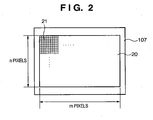
- FIG. 2 is a plan view of light-receiving pixels, on which an object image is formed, of the image sensor 107 of FIG. 1 , as viewed from the photographing lens 100 side.
- 20 indicates an entire pixel area including m pixels in the lateral direction and n pixels in the longitudinal direction formed on the image sensor 107, and one of the pixel portions is indicated by 21.
- primary color filters in a Bayer arrangement are formed on-chip, that is, a 2 ⁇ 2 pixel group including four pixels is repeatedly arranged. For the sake of simplifying the drawing, only the pixel portion that is formed of 10 ⁇ 10 pixels is shown on the upper left side of FIG. 2 , and other pixel portions are omitted.
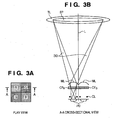
- FIGS. 3A, 3B , 4A and 4B are diagrams illustrating a structure of image sensing pixels and focus detection pixels of the pixel portion shown in FIG. 2 .
- a Bayer arrangement is adopted, that is, in 2 ⁇ 2 pixel groups including four pixels, two pixels that have a G (green) spectral sensitivity are arranged diagonally, and one pixel that has an R (red) spectral sensitivity and one pixel that has a B (blue) spectral sensitivity are arranged diagonally.
- focus detection pixels that have a structure described later are arranged between such Bayer blocks.
- the photographing lens 100 is schematically shown as a TL (taking lens), and L indicates the optical axis of the photographing lens TL.
- FIGS. 3A and 3B are diagrams showing a structure of the pixels in the vicinity of the center of the image sensor 107, that is, the pixels in the vicinity of the axis of the photographing lens TL.
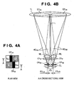
- FIGS. 4A and 4B show the arrangement and structure of focus detection pixels for dividing the pupil in the horizontal direction (lateral direction) of the photographing lens TL.
- the horizontal direction refers to a lengthwise direction of the image sensor 107 shown in FIG. 2 .
- FIG. 4A is a plan view of 2 ⁇ 2 pixels including focus detection pixels.
- the offset amount 51 HB is set to be larger than the offset amount 51 HA .
- offsetting in the peripheral portion in the horizontal direction was described as an example, but pupil division can also be realized on the peripheral portion in the vertical direction, and on the peripheral portion in both the horizontal and vertical directions, using the same method.
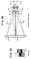
- FIG. 6B shows a cross-sectional view taken along the A-A line of FIG. 6A .
- the structure of the pixels shown in Fig. 6B are the same as that of the pixels shown in Fig. 4B except that the focus detection pixels of FIG. 4B have a structure of dividing the pupil in the lateral direction, while the focus detection pixels of FIG. 6B have a structure of dividing the pupil in the longitudinal direction.
- An opening OP VC of a pixel S VC is offset to the lower side from the center line of the microlens ML by an amount 61 VC , so that light beams 60 VC that have passed through an exit pupil region EP VC located on the upper side of the optical axis L of the photographing lens TL are received.
- an opening OP VD of a pixel S VD is offset to the upper side from the center line of the microlens ML by an amount 61 VD , so that light beams 60 VD that have passed through an exit pupil region EP VD located in the lower side of the optical axis L of the photographing lens TL are received.
- the offset amount 61 VC and the offset amount 61 VD are equal because FIGS. 6A and 6B show the structure of the pixels in the vicinity of the axis of the image sensor 107 as in FIGS. 4A and 4B .
- the focus detection pixel pair S HA and S HB and the focus detection pixel pair S VC and S VD do not have color information, when forming a photographed image, interpolation computation is performed using the signals of the neighboring pixels so as to create a signal. Accordingly, by arranging the focus detection pixel pairs discretely in the image sensor 107 rather than continuously, the quality of photographed images is not reduced.
- the image sensor 107 functions not only as an image sensor, but also as a focus detection unit of the present invention.
- the CPU 121 includes a combining unit 902, a connecting unit 903, and a computation unit 904. Also, the CPU 121 assigns a plurality of sections (regions) CST on the image sensing surface of the image sensor 107 so as to include a plurality of focus detection units 901. The CPU 121 can change the size, arrangement, number and the like of the sections CST as appropriate.
- the combining unit 902 performs a process of obtaining one pixel's worth of a first combined signal by combining the output signals from the first focus detection pixels 901a for each of the plurality of sections CST assigned on the image sensor 107.
- FIG. 7 an example in which the pupil is divided in the horizontal direction is given, but the same can apply to the case in which the pupil is divided in the vertical direction.
- FIG. 8 shows an example of a focus detection signal pair (image signal pair) that is formed by the focus detection unit 901, the combining unit 902 and the connecting unit 903 and inputted into the computation unit 904 of FIG. 7 .
- the lateral axis indicates positions of pixels in the direction in which the pixels of the connected signal are arranged, and the longitudinal axis indicates the signal intensity.
- the focus detection signals shown in FIG. 8 are signals obtained by sensing a single vertical line.
- a focus detection signal IMG A is a signal formed by focus detection pixels 901a
- a focus detection signal IMG B is a signal formed by focus detection pixels 901b.
- the photographing lens 100 shown in FIG. 1 is shifted to the rear focus side with respect to the image sensor 107, the focus detection signal IMG A is shifted to the left side, and the focus detection signal IMG B is shifted to the right side.
- FIG. 8 was described taking the case in which the lens is shifted to the rear focus side as an example, but when the lens is shifted to the front focus side, the directions in which the focus detection signals IMG A and IMG B shift are laterally reversed.
- FIG. 9 is a diagram conceptually illustrating a pupil-dividing function realized by the focus detection pixels of the image sensor 107.
- TL denotes a photographing lens
- 107 denotes the image sensor
- OBJ denotes an object
- IMG denotes an object image.
- the pixels S HB , Svc and S VD receive light beams that have passed through the exit pupil regions EP HB , EP VC and EP VD , respectively. Because the focus detection pixels are distributed over the entire region of the image sensor 107, focus detection is possible in the entire image sensing region as well. With the configuration as described above, it is possible to perform focus detection using the phase-difference method over a wide area of the image sensor 107.
- FIG. 10 is a diagram schematically illustrating a layered CMOS sensor chip that is included in the image sensor 107 of FIG. 1 .
- a pad insulating layer is formed on a lower layer in which a photodiode and a transistor are formed so as to form unit pixels.
- the pad insulating layer is selectively removed so as to expose the metal wiring of the lower layer.
- the metal wiring is used to connect the transistor to an external element.
- a plurality of such wiring and insulating layers are formed. In FIG. 10 , they are collectively shown as a wiring/insulating layer 11. That is, the wiring layer CL of FIGS. 4A to 6B is also included in the wiring/insulating layer 11.
- a color photoresist is applied, and the resultant is exposed and developed to form a color filter layer 12.
- a microlens planarization layer 13 is formed so that uniform microlenses can be formed.
- a photoresist is applied onto the microlens planarization layer 13, and this is exposed and developed to form a patterned photoresist.
- the patterned photoresist is heat-treated to reflow the photoresist so as to form a layer of dome-shaped microlenses 14.
- the CMOS sensor chip is produced layer by layer, so production errors occur between layers.
- the positional accuracy of the microlens 14 with respect to the wiring/insulating layer 11 depends on the alignment accuracy of the semiconductor manufacturing apparatus that forms the patterned photoresist. That is, a shift of the microlens ML with respect to the wiring layer CL shown in FIGS. 4A to 6B is caused by such alignment inaccuracies.
- the distance between the microlens ML and the photodiode PD is several micrometers.
- the distance from the microlens ML to the exit pupil of the photographing lens 100 is expressed in units of several tens of millimeters. Accordingly, the optical imaging magnification will be several ten thousand-fold. If, for example, an alignment error of 0.1 micrometers occurs, it results in a very large shift of several millimeters in the exit pupil, causing the focus detection accuracy to decrease significantly.
- FIG. 11 shows the focus detection pixels for dividing the pupil in the horizontal direction (lateral direction) of the photographing lens shown in FIG. 4B , in which an alignment error in the horizontal direction has occurred in the microlens ML.
- the microlens ML is shifted to the left by an amount D ML
- a microlens ML indicated by the dotted line shows the position when there is no alignment error ( FIG. 4B ). That is, the shift amount D ML of FIG. 11 is added to and subtracted from the offset amounts 41 HA and 41 HB of FIG.
- the pixels S HA and S HB receive light beams 120 HA and 120 HB , respectively, that correspond to the exit pupil regions EP HA and EP HB , which have shifted from the optical axis L of the photographing lens TL by an amount D EP .
- the center L AF of the focus detection exit pupil regions EP HA , EP HB , EP VC and EP VD is located in a position shifted from the optical axis L of the photographing lens TL by an amount D EP .
- L AF serves as the center axis of the focus detection unit of the present invention, and D EP corresponds to a central axis shift.
- Common regions in which the exit pupil EP overlaps with the focus detection exit pupil regions EP HA and EP HE that is, regions through which light beams used for focus detection actually pass are indicated by right-diagonally shaded regions 130 HA and 130 HB as shown in FIG. 13A .
- the diagonally shaded regions 130 HA and 130 HB are asymmetric to each other in the horizontal direction that is the pupil-dividing direction due to the central axis shift D EP .
- FIG. 16 is a diagram showing the image sensor 107 and exit pupil shapes depending on the corresponding image height of the image sensor 107.
- EP C indicates an exit pupil shape on the axis
- the subscripts T, B, L and R indicate image heights on the upper, lower, right and left sides, respectively.
- an exit pupil shape at the upper left corner is indicated by EP TL by combining T and L.
- the exit pupil shape becomes smaller as the image height increases from the center of the image sensor 107.
- a focus detection region is set to a region 160 indicated by the dotted line in FIG. 16 , where the exit pupil shape changes relatively little in the full zoom/focus positions.
- favorable focus detection capable of detecting the further edge of the photographing screen can be performed.
- exit pupil regions of the exit pupil are determined by combining a central axis shift caused by a microlens alignment error and a change in the exit pupil shape of the photographing lens depending on the image height.
- the phase-difference focus detection method when such a change occurs in the exit pupil region, the following three main problems arise.
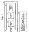
- FIG. 17 is a block diagram showing the detailed internal configuration of the computation unit 904 for correcting a focus detection signal pair in Embodiment 1 that is provided in the CPU 121 of FIG. 7 .
- the focus detection signal formed by the connecting unit 903 of FIG. 7 is subjected to a correction including a correction of the problem (1) by a correction unit 170 of the computation unit 904 and, after that, inputted into a correlation computation unit 171.
- the flash memory 133 connected to the CPU 121 stores pixel non-uniform sensitivity information 175 of the pixels that form a focus detection signal, exit pupil information 176 created from the image height of the photographing lens 100, and central axis shift information 177 created from a microlens alignment error.
- the pixel non-uniform sensitivity information 175 and the central axis shift information 177 are pieces of information written during the production process of the camera.
- the exit pupil information 176 contains in advance information under error-free design values.
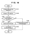
- FIG. 18 is a flowchart illustrating a procedure for correcting a focus detection signal according to Embodiment 1 of the present invention.
- the correction unit 170 performs a two-stage correction on a pair of focus detection signals inputted therein in steps S181 and S182.
- the correlation computation unit 171 performs processes spanning from step S183 to S186.
- step S181 the non-uniform sensitivity of each pixel is corrected by multiplying the output value data of each pixel by a coefficient for correcting the non-uniform sensitivity based on the pixel non-uniform sensitivity information 175 stored in the flash memory 133.
- step S182 for each pair of pixels that form a pair of focus detection signals, the areas of the diagonally shaded regions as described in FIGS. 13A and 14A are calculated from the exit pupil information 176 and the central axis shift information 177. Then, the coefficients corresponding to the calculated areas are multiplied by the output value of each pixel so as to correct the amount of light.
- the following method is employed to reduce the amount of computation.
- f(x,y) is pre-stored as exit pupil information 176
- (x ERR ,y ERR ) and g(x ERR ,y ERR ) are pre-stored as central axis shift information 177.
- a correction with a reduced amount of computation becomes possible.
- the production error (x EAA ,y EAA )
- such a microlens alignment error is dominant.
- an alignment error is a uniform shift in each wafer.
- the need to check alignment errors for each device can be eliminated and, as a result, the process can be shortened.
- Other examples of the production error (x ERR ,y ERR ) include position alignment errors such as parallel axis offsets, inclination offsets and the like that can occur when the image sensor 107 is assembled in a camera.
- step S183 it is determined whether or not the focus detection signal corrected by the correction unit 170 is sufficiently reliable before subjecting the focus detection signal to the subsequent processes. Specifically, such a determination is performed by analyzing a contrast component of the image or the like.
- Embodiment 2 of the present invention will be described next.
- Embodiment 2 differs from Embodiment 1 in that Embodiment 2 can cope with the case in which, in the photographing lens 100, the pupil distance changes significantly depending on the zoom or focus position.
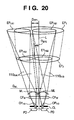
- FIG. 20 is a diagram for illustrating such a case, and shows focus detection pixels that correspond to the focus detection pixels of Embodiment 1 shown in FIG. 11 .
- EP 1 indicates an exit pupil when the zoom position of the photographing lens 100 is at a telephoto end
- EP 2 indicates the exit pupil when the zoom position of the photographing lens 100 is at a wide-angle end.
- the exit pupil changes in a range indicated by dotted lines in FIG. 20 between the telephoto end and the wide-angle end.
- Embodiment 2 not only the diameter of the exit pupil changes according to the zoom position of the photographing lens 100, but also the distance from the microlens to the exit pupil, or in other words, the exit pupil distance changes. Accordingly, a shift D EP1 of the exit pupil regions EP HA1 and EP HB1 and a shift D EP2 of the exit pupil regions EP HA2 and EP HB2 that are caused by a microlens ML alignment error D ML differ between the exit pupils EP 1 and EP 2 .
- FIGS. 21A and 21B are diagrams of the exit pupil of the pixels in the vicinity of the axis of the image sensor 107 of FIG. 20 as viewed from the image sensor 107 side, with FIG. 21A showing the telephoto end side and FIG. 21B showing the wide-angle end side.
- the center L AF1 of the focus detection exit pupil regions EP HA1 and EP HB1 and the center L AF2 of the focus detection exit pupil regions EP HA2 and EP HB2 are located in a position shifted from the optical axis L of the photographing lens TL by the amounts D EP1 and D EP2 , respectively.
- L AF1 and L AF2 serve as the center axis of the focus detection unit in the exit pupils EP 1 and EP 2 , respectively, and D EP1 and D EP2 correspond to central axis shifts.
- Common regions in which the exit pupil EP 1 overlaps with the focus detection exit pupil regions EP HA1 and EP HB1 , and common regions in which the exit pupil EP 2 overlaps with the focus detection exit pupil regions EP HA2 and EP HB2 , that is, the regions through which light beams that are actually used for focus detection pass are indicated by right-diagonally shaded regions 210 HA1 and 210 HB1 , and 211 HA2 and 211 HB2 , respectively.
- the light amount ratios of the focus detection pixel pair are different on the telephoto end side and the wide-angle end side. This is because in addition to a change of the exit pupil from EP 1 to EP 2 , the central axis shift changes from D EP1 to D EP2 .
- FIGS. 20 , 21A and 21B are described in the context of the pixels in the vicinity of the axis of the image sensor 107, in the peripheral portion, the degree of change in the central axis shift is different. Accordingly, it is necessary to store central axis shift information in a format associated with a change in the exit pupil distance rather than storing central axis shift information regarding one exit pupil as in Embodiment 1.
- a central axis shift (x ERR ,y ERR ) in an arbitrary pixel position (x,y) of the image sensor 107 can be expressed by the following Equations (4) and (5) as a function of the distance 1 and the pixel position (x,y).
- x ERR h l ⁇ x y
- ERR i l ⁇ y
- the amount of light can be corrected.
- the central axis shifts D EP1 and D EP2 at the distances to the two exit pupils EP 1 and EP 2 as shown in FIG. 20 are measured at a plurality of image heights. By doing so, h(l,x) and i(l,y) can be determined easily.
- f(x,y) and g(x ERR ,y ERR ) of Equation 3 are also configured to be stored for each zoom position.
- Embodiment 3 shows an example in which the focus detection unit of Embodiment 1 is applied to a camera system.
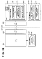
- FIG. 22 is a block diagram showing a configuration of a camera system according to Embodiment 3.
- 220 denotes a camera body
- 221 denotes an interchangeable lens detachable from the camera body 220, and they are joined so as to be capable of information communication via I/F units 222 and 223.
- the interchangeable lens 221 includes a CPU 224 that performs various computation processes, and that is connected to a driving circuit 225 that drives the zoom, focus, diaphragm shutter and the like of the photographing lens 100.
- the driving circuit 225 is connected to an actuator 226.
- a flash memory 227 into which various pieces of information can be rewritten is also included in the interchangeable lens 221.
- FIG. 23 is a block diagram of a part of the block diagram of FIG. 22 that is relevant to the present embodiment so as to illustrate it in further detail.
- the camera body 220 is shown on the right side of the dotted center line, and the interchangeable lens 221 (lens unit) is shown on the left side of the same.
- the flash memory 133 of the camera body 220 includes only pixel non-uniform sensitivity information 175 and central axis shift information 177, and the flash memory 227 of the interchangeable lens 221 includes exit pupil information 176. Accordingly, even when a different type of lens is attached as the interchangeable lens 221, the exit pupil information 176 of that lens can be acquired via the I/F units 222 and 223.
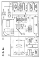
- Embodiment 4 of the present invention will be described next.
- Embodiment 4 shows an example in which the present invention is applied to a camera system that includes a secondary imaging type focus detection unit of a phase-difference method, in comparison with Embodiment 1.
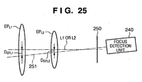
- FIG. 25 is a conceptual diagram showing the relationship between the focus detection unit 240 and the exit pupils of various interchangeable lenses, and is an exploded view in which the main mirror 241 and the sub-mirror 242 of FIG. 24 are omitted.
- EP L1 indicates the exit pupil of an interchangeable lens
- EP L2 indicates the exit pupil of another interchangeable lens.
- L1 and L2 indicate the optical axes of these interchangeable lenses, and are shown as a single line in FIG. 25 because the two optical axes are overlapping.
- 250 indicates a primary imaging surface that is the focal surface of the interchangeable lenses, disposed in a position optically equivalent to the image sensing surface of the image sensor 107 of FIG. 24 .
- the focus detection unit 240 is disposed in the rear of the primary imaging surface 250, with a center axis 251 of the focus detection unit 240 indicated by a long dashed short dashed line.
- the center axis 251 is shifted from the optical axes L1 and L2 by a production error, creating a central axis shift D EPL1 on the exit pupil EP L1 , and a central axis shift D EPL2 on the exit pupil EP L2 . That is, this indicates that when the center axis 251 of the focus detection unit 240 shifts, in the camera system to which various photographing lenses with different exit pupils can be attached, the central axis shift varies depending on the exit pupil distance. Accordingly, by pre-storing central axis shift information in a format associated with such exit pupil distances in the camera, highly accurate focus detection can be performed by the method described in Embodiment 2.
- the central axis shift described in Embodiment 4 can occur through a positional error of the main mirror 241 or the sub-mirror 242, a production error in the field lens of the focus detection unit 240, or the like.
- a mechanism that adjusts the central axis shift of the focus detection unit 240 is provided so as to perform adjustment during assembly/production thereof, but by applying Embodiment 4, the need for such a mechanism can be eliminated, achieving the effect of reduced costs.
Landscapes
- Physics & Mathematics (AREA)
- General Physics & Mathematics (AREA)
- Engineering & Computer Science (AREA)
- Multimedia (AREA)
- Signal Processing (AREA)
- Optics & Photonics (AREA)
- Automatic Focus Adjustment (AREA)
- Focusing (AREA)
- Studio Devices (AREA)
Priority Applications (3)
| Application Number | Priority Date | Filing Date | Title |
|---|---|---|---|
| EP22157059.1A EP4047416B1 (en) | 2008-08-25 | 2009-08-24 | Image sensing apparatus, camera system and control method |
| EP18159802.0A EP3396449A1 (en) | 2008-08-25 | 2009-08-24 | Image sensing apparatus and control method |
| EP14178618.6A EP2811340B1 (en) | 2008-08-25 | 2009-08-24 | Image sensing apparatus, image sensing system and focus detection method |
Applications Claiming Priority (1)
| Application Number | Priority Date | Filing Date | Title |
|---|---|---|---|
| JP2008215918A JP5161702B2 (ja) | 2008-08-25 | 2008-08-25 | 撮像装置、撮像システム、及び焦点検出方法 |
Related Child Applications (4)
| Application Number | Title | Priority Date | Filing Date |
|---|---|---|---|
| EP18159802.0A Division EP3396449A1 (en) | 2008-08-25 | 2009-08-24 | Image sensing apparatus and control method |
| EP14178618.6A Division-Into EP2811340B1 (en) | 2008-08-25 | 2009-08-24 | Image sensing apparatus, image sensing system and focus detection method |
| EP14178618.6A Division EP2811340B1 (en) | 2008-08-25 | 2009-08-24 | Image sensing apparatus, image sensing system and focus detection method |
| EP22157059.1A Division EP4047416B1 (en) | 2008-08-25 | 2009-08-24 | Image sensing apparatus, camera system and control method |
Publications (3)
| Publication Number | Publication Date |
|---|---|
| EP2169459A2 EP2169459A2 (en) | 2010-03-31 |
| EP2169459A3 EP2169459A3 (en) | 2011-04-06 |
| EP2169459B1 true EP2169459B1 (en) | 2014-10-08 |
Family
ID=41667536
Family Applications (4)
| Application Number | Title | Priority Date | Filing Date |
|---|---|---|---|
| EP09168519.8A Not-in-force EP2169459B1 (en) | 2008-08-25 | 2009-08-24 | Image sensing apparatus, image sensing system and focus detection method |
| EP14178618.6A Not-in-force EP2811340B1 (en) | 2008-08-25 | 2009-08-24 | Image sensing apparatus, image sensing system and focus detection method |
| EP22157059.1A Active EP4047416B1 (en) | 2008-08-25 | 2009-08-24 | Image sensing apparatus, camera system and control method |
| EP18159802.0A Withdrawn EP3396449A1 (en) | 2008-08-25 | 2009-08-24 | Image sensing apparatus and control method |
Family Applications After (3)
| Application Number | Title | Priority Date | Filing Date |
|---|---|---|---|
| EP14178618.6A Not-in-force EP2811340B1 (en) | 2008-08-25 | 2009-08-24 | Image sensing apparatus, image sensing system and focus detection method |
| EP22157059.1A Active EP4047416B1 (en) | 2008-08-25 | 2009-08-24 | Image sensing apparatus, camera system and control method |
| EP18159802.0A Withdrawn EP3396449A1 (en) | 2008-08-25 | 2009-08-24 | Image sensing apparatus and control method |
Country Status (4)
| Country | Link |
|---|---|
| US (3) | US8405760B2 (enExample) |
| EP (4) | EP2169459B1 (enExample) |
| JP (1) | JP5161702B2 (enExample) |
| CN (1) | CN101662588B (enExample) |
Families Citing this family (244)
| Publication number | Priority date | Publication date | Assignee | Title |
|---|---|---|---|---|
| US8279318B2 (en) * | 2007-12-14 | 2012-10-02 | Canon Kabushiki Kaisha | Image pickup apparatus and display control method for the same |
| KR20100138614A (ko) * | 2009-06-25 | 2010-12-31 | 삼성전자주식회사 | 자동초점 검출장치 및 이를 적용한 카메라 |
| JP5662667B2 (ja) * | 2009-10-08 | 2015-02-04 | キヤノン株式会社 | 撮像装置 |
| US10910364B2 (en) | 2009-10-12 | 2021-02-02 | Monolitaic 3D Inc. | 3D semiconductor device |
| US10366970B2 (en) | 2009-10-12 | 2019-07-30 | Monolithic 3D Inc. | 3D semiconductor device and structure |
| US10157909B2 (en) | 2009-10-12 | 2018-12-18 | Monolithic 3D Inc. | 3D semiconductor device and structure |
| US11018133B2 (en) | 2009-10-12 | 2021-05-25 | Monolithic 3D Inc. | 3D integrated circuit |
| US10354995B2 (en) | 2009-10-12 | 2019-07-16 | Monolithic 3D Inc. | Semiconductor memory device and structure |
| US10388863B2 (en) | 2009-10-12 | 2019-08-20 | Monolithic 3D Inc. | 3D memory device and structure |
| US10043781B2 (en) | 2009-10-12 | 2018-08-07 | Monolithic 3D Inc. | 3D semiconductor device and structure |
| US11984445B2 (en) | 2009-10-12 | 2024-05-14 | Monolithic 3D Inc. | 3D semiconductor devices and structures with metal layers |
| US12027518B1 (en) | 2009-10-12 | 2024-07-02 | Monolithic 3D Inc. | 3D semiconductor devices and structures with metal layers |
| US11374118B2 (en) | 2009-10-12 | 2022-06-28 | Monolithic 3D Inc. | Method to form a 3D integrated circuit |
| JP5537905B2 (ja) * | 2009-11-10 | 2014-07-02 | 富士フイルム株式会社 | 撮像素子及び撮像装置 |
| JP2011221253A (ja) | 2010-04-08 | 2011-11-04 | Sony Corp | 撮像装置、固体撮像素子、撮像方法およびプログラム |
| JP5642433B2 (ja) * | 2010-06-15 | 2014-12-17 | 富士フイルム株式会社 | 撮像装置及び画像処理方法 |
| US10217667B2 (en) | 2011-06-28 | 2019-02-26 | Monolithic 3D Inc. | 3D semiconductor device, fabrication method and system |
| JP5676988B2 (ja) * | 2010-09-14 | 2015-02-25 | キヤノン株式会社 | 焦点調節装置 |
| US11482440B2 (en) | 2010-12-16 | 2022-10-25 | Monolithic 3D Inc. | 3D semiconductor device and structure with a built-in test circuit for repairing faulty circuits |
| US12362219B2 (en) | 2010-11-18 | 2025-07-15 | Monolithic 3D Inc. | 3D semiconductor memory device and structure |
| US10497713B2 (en) | 2010-11-18 | 2019-12-03 | Monolithic 3D Inc. | 3D semiconductor memory device and structure |
| US11227897B2 (en) | 2010-10-11 | 2022-01-18 | Monolithic 3D Inc. | Method for producing a 3D semiconductor memory device and structure |
| US10896931B1 (en) | 2010-10-11 | 2021-01-19 | Monolithic 3D Inc. | 3D semiconductor device and structure |
| US11257867B1 (en) | 2010-10-11 | 2022-02-22 | Monolithic 3D Inc. | 3D semiconductor device and structure with oxide bonds |
| US11600667B1 (en) | 2010-10-11 | 2023-03-07 | Monolithic 3D Inc. | Method to produce 3D semiconductor devices and structures with memory |
| US11158674B2 (en) | 2010-10-11 | 2021-10-26 | Monolithic 3D Inc. | Method to produce a 3D semiconductor device and structure |
| US11024673B1 (en) | 2010-10-11 | 2021-06-01 | Monolithic 3D Inc. | 3D semiconductor device and structure |
| US10290682B2 (en) | 2010-10-11 | 2019-05-14 | Monolithic 3D Inc. | 3D IC semiconductor device and structure with stacked memory |
| US11469271B2 (en) | 2010-10-11 | 2022-10-11 | Monolithic 3D Inc. | Method to produce 3D semiconductor devices and structures with memory |
| US11315980B1 (en) | 2010-10-11 | 2022-04-26 | Monolithic 3D Inc. | 3D semiconductor device and structure with transistors |
| US11018191B1 (en) | 2010-10-11 | 2021-05-25 | Monolithic 3D Inc. | 3D semiconductor device and structure |
| US11327227B2 (en) | 2010-10-13 | 2022-05-10 | Monolithic 3D Inc. | Multilevel semiconductor device and structure with electromagnetic modulators |
| US11404466B2 (en) | 2010-10-13 | 2022-08-02 | Monolithic 3D Inc. | Multilevel semiconductor device and structure with image sensors |
| US11164898B2 (en) | 2010-10-13 | 2021-11-02 | Monolithic 3D Inc. | Multilevel semiconductor device and structure |
| US11855100B2 (en) | 2010-10-13 | 2023-12-26 | Monolithic 3D Inc. | Multilevel semiconductor device and structure with oxide bonding |
| US12080743B2 (en) | 2010-10-13 | 2024-09-03 | Monolithic 3D Inc. | Multilevel semiconductor device and structure with image sensors and wafer bonding |
| US10679977B2 (en) | 2010-10-13 | 2020-06-09 | Monolithic 3D Inc. | 3D microdisplay device and structure |
| US11163112B2 (en) | 2010-10-13 | 2021-11-02 | Monolithic 3D Inc. | Multilevel semiconductor device and structure with electromagnetic modulators |
| US12360310B2 (en) | 2010-10-13 | 2025-07-15 | Monolithic 3D Inc. | Multilevel semiconductor device and structure with oxide bonding |
| US11605663B2 (en) | 2010-10-13 | 2023-03-14 | Monolithic 3D Inc. | Multilevel semiconductor device and structure with image sensors and wafer bonding |
| US11043523B1 (en) | 2010-10-13 | 2021-06-22 | Monolithic 3D Inc. | Multilevel semiconductor device and structure with image sensors |
| US11929372B2 (en) | 2010-10-13 | 2024-03-12 | Monolithic 3D Inc. | Multilevel semiconductor device and structure with image sensors and wafer bonding |
| US11063071B1 (en) | 2010-10-13 | 2021-07-13 | Monolithic 3D Inc. | Multilevel semiconductor device and structure with waveguides |
| US10998374B1 (en) | 2010-10-13 | 2021-05-04 | Monolithic 3D Inc. | Multilevel semiconductor device and structure |
| US10833108B2 (en) | 2010-10-13 | 2020-11-10 | Monolithic 3D Inc. | 3D microdisplay device and structure |
| US11694922B2 (en) | 2010-10-13 | 2023-07-04 | Monolithic 3D Inc. | Multilevel semiconductor device and structure with oxide bonding |
| US11855114B2 (en) | 2010-10-13 | 2023-12-26 | Monolithic 3D Inc. | Multilevel semiconductor device and structure with image sensors and wafer bonding |
| US9941319B2 (en) * | 2010-10-13 | 2018-04-10 | Monolithic 3D Inc. | Semiconductor and optoelectronic methods and devices |
| US12094892B2 (en) | 2010-10-13 | 2024-09-17 | Monolithic 3D Inc. | 3D micro display device and structure |
| US11437368B2 (en) | 2010-10-13 | 2022-09-06 | Monolithic 3D Inc. | Multilevel semiconductor device and structure with oxide bonding |
| US11133344B2 (en) | 2010-10-13 | 2021-09-28 | Monolithic 3D Inc. | Multilevel semiconductor device and structure with image sensors |
| US11984438B2 (en) | 2010-10-13 | 2024-05-14 | Monolithic 3D Inc. | Multilevel semiconductor device and structure with oxide bonding |
| US10978501B1 (en) | 2010-10-13 | 2021-04-13 | Monolithic 3D Inc. | Multilevel semiconductor device and structure with waveguides |
| US10943934B2 (en) | 2010-10-13 | 2021-03-09 | Monolithic 3D Inc. | Multilevel semiconductor device and structure |
| US11869915B2 (en) | 2010-10-13 | 2024-01-09 | Monolithic 3D Inc. | Multilevel semiconductor device and structure with image sensors and wafer bonding |
| JP5614227B2 (ja) * | 2010-10-18 | 2014-10-29 | 株式会社ニコン | 焦点検出装置及び撮像装置 |
| US11482439B2 (en) | 2010-11-18 | 2022-10-25 | Monolithic 3D Inc. | Methods for producing a 3D semiconductor memory device comprising charge trap junction-less transistors |
| US11615977B2 (en) | 2010-11-18 | 2023-03-28 | Monolithic 3D Inc. | 3D semiconductor memory device and structure |
| US12154817B1 (en) | 2010-11-18 | 2024-11-26 | Monolithic 3D Inc. | Methods for producing a 3D semiconductor memory device and structure |
| US12033884B2 (en) | 2010-11-18 | 2024-07-09 | Monolithic 3D Inc. | Methods for producing a 3D semiconductor device and structure with memory cells and multiple metal layers |
| US11211279B2 (en) | 2010-11-18 | 2021-12-28 | Monolithic 3D Inc. | Method for processing a 3D integrated circuit and structure |
| US12068187B2 (en) | 2010-11-18 | 2024-08-20 | Monolithic 3D Inc. | 3D semiconductor device and structure with bonding and DRAM memory cells |
| US11901210B2 (en) | 2010-11-18 | 2024-02-13 | Monolithic 3D Inc. | 3D semiconductor device and structure with memory |
| US11443971B2 (en) | 2010-11-18 | 2022-09-13 | Monolithic 3D Inc. | 3D semiconductor device and structure with memory |
| US11923230B1 (en) | 2010-11-18 | 2024-03-05 | Monolithic 3D Inc. | 3D semiconductor device and structure with bonding |
| US11031275B2 (en) | 2010-11-18 | 2021-06-08 | Monolithic 3D Inc. | 3D semiconductor device and structure with memory |
| US11521888B2 (en) | 2010-11-18 | 2022-12-06 | Monolithic 3D Inc. | 3D semiconductor device and structure with high-k metal gate transistors |
| US11495484B2 (en) | 2010-11-18 | 2022-11-08 | Monolithic 3D Inc. | 3D semiconductor devices and structures with at least two single-crystal layers |
| US11355380B2 (en) | 2010-11-18 | 2022-06-07 | Monolithic 3D Inc. | Methods for producing 3D semiconductor memory device and structure utilizing alignment marks |
| US12100611B2 (en) | 2010-11-18 | 2024-09-24 | Monolithic 3D Inc. | Methods for producing a 3D semiconductor device and structure with memory cells and multiple metal layers |
| US11094576B1 (en) | 2010-11-18 | 2021-08-17 | Monolithic 3D Inc. | Methods for producing a 3D semiconductor memory device and structure |
| US11004719B1 (en) | 2010-11-18 | 2021-05-11 | Monolithic 3D Inc. | Methods for producing a 3D semiconductor memory device and structure |
| US12272586B2 (en) | 2010-11-18 | 2025-04-08 | Monolithic 3D Inc. | 3D semiconductor memory device and structure with memory and metal layers |
| US11610802B2 (en) | 2010-11-18 | 2023-03-21 | Monolithic 3D Inc. | Method for producing a 3D semiconductor device and structure with single crystal transistors and metal gate electrodes |
| US11355381B2 (en) | 2010-11-18 | 2022-06-07 | Monolithic 3D Inc. | 3D semiconductor memory device and structure |
| US12136562B2 (en) | 2010-11-18 | 2024-11-05 | Monolithic 3D Inc. | 3D semiconductor device and structure with single-crystal layers |
| US11107721B2 (en) | 2010-11-18 | 2021-08-31 | Monolithic 3D Inc. | 3D semiconductor device and structure with NAND logic |
| US11862503B2 (en) | 2010-11-18 | 2024-01-02 | Monolithic 3D Inc. | Method for producing a 3D semiconductor device and structure with memory cells and multiple metal layers |
| US11164770B1 (en) | 2010-11-18 | 2021-11-02 | Monolithic 3D Inc. | Method for producing a 3D semiconductor memory device and structure |
| US11508605B2 (en) | 2010-11-18 | 2022-11-22 | Monolithic 3D Inc. | 3D semiconductor memory device and structure |
| US12125737B1 (en) | 2010-11-18 | 2024-10-22 | Monolithic 3D Inc. | 3D semiconductor device and structure with metal layers and memory cells |
| US11784082B2 (en) | 2010-11-18 | 2023-10-10 | Monolithic 3D Inc. | 3D semiconductor device and structure with bonding |
| US11804396B2 (en) | 2010-11-18 | 2023-10-31 | Monolithic 3D Inc. | Methods for producing a 3D semiconductor device and structure with memory cells and multiple metal layers |
| US12144190B2 (en) | 2010-11-18 | 2024-11-12 | Monolithic 3D Inc. | 3D semiconductor device and structure with bonding and memory cells preliminary class |
| US11854857B1 (en) | 2010-11-18 | 2023-12-26 | Monolithic 3D Inc. | Methods for producing a 3D semiconductor device and structure with memory cells and multiple metal layers |
| US11735462B2 (en) | 2010-11-18 | 2023-08-22 | Monolithic 3D Inc. | 3D semiconductor device and structure with single-crystal layers |
| US11121021B2 (en) | 2010-11-18 | 2021-09-14 | Monolithic 3D Inc. | 3D semiconductor device and structure |
| US12243765B2 (en) | 2010-11-18 | 2025-03-04 | Monolithic 3D Inc. | 3D semiconductor device and structure with metal layers and memory cells |
| US11569117B2 (en) | 2010-11-18 | 2023-01-31 | Monolithic 3D Inc. | 3D semiconductor device and structure with single-crystal layers |
| US11482438B2 (en) | 2010-11-18 | 2022-10-25 | Monolithic 3D Inc. | Methods for producing a 3D semiconductor memory device and structure |
| US11018042B1 (en) | 2010-11-18 | 2021-05-25 | Monolithic 3D Inc. | 3D semiconductor memory device and structure |
| US12463076B2 (en) | 2010-12-16 | 2025-11-04 | Monolithic 3D Inc. | 3D semiconductor device and structure |
| JP5663331B2 (ja) * | 2011-01-31 | 2015-02-04 | オリンパス株式会社 | 制御装置、内視鏡装置、絞り制御方法及びプログラム |
| JP2012234152A (ja) * | 2011-04-19 | 2012-11-29 | Canon Inc | 撮像装置及びその制御方法 |
| JP5791349B2 (ja) * | 2011-04-21 | 2015-10-07 | キヤノン株式会社 | 撮像装置及びその制御方法 |
| KR101777351B1 (ko) | 2011-05-16 | 2017-09-11 | 삼성전자주식회사 | 촬상 소자, 이를 이용한 디지털 촬영 장치, 오토 포커싱 방법, 및 상기 방법을 수행하기 위한 컴퓨터 판독가능 저장매체 |
| JP5956782B2 (ja) * | 2011-05-26 | 2016-07-27 | キヤノン株式会社 | 撮像素子及び撮像装置 |
| KR101747304B1 (ko) * | 2011-05-30 | 2017-06-14 | 삼성전자주식회사 | 디지털 촬영 장치, 오토포커싱 방법, 및 이를 실행하기 위한 컴퓨터 판독가능 저장매체 |
| US10388568B2 (en) | 2011-06-28 | 2019-08-20 | Monolithic 3D Inc. | 3D semiconductor device and system |
| JP5784395B2 (ja) * | 2011-07-13 | 2015-09-24 | オリンパス株式会社 | 撮像装置 |
| US8810713B2 (en) * | 2011-07-13 | 2014-08-19 | Olympus Imaging Corp. | Image pickup apparatus and image pickup device for performing auto-focusing |
| KR101853817B1 (ko) * | 2011-07-20 | 2018-05-02 | 삼성전자주식회사 | 촬상 소자 |
| JP6000520B2 (ja) | 2011-07-25 | 2016-09-28 | キヤノン株式会社 | 撮像装置およびその制御方法およびプログラム |
| WO2013027507A1 (ja) * | 2011-08-23 | 2013-02-28 | 富士フイルム株式会社 | 撮像装置 |
| CN103930826B (zh) * | 2011-09-13 | 2016-12-28 | 富士胶片株式会社 | 立体摄像装置 |
| GB201119206D0 (en) | 2011-11-07 | 2011-12-21 | Canon Kk | Method and device for providing compensation offsets for a set of reconstructed samples of an image |
| JP5914055B2 (ja) * | 2012-03-06 | 2016-05-11 | キヤノン株式会社 | 撮像装置 |
| CN104221369B (zh) * | 2012-03-28 | 2016-02-10 | 富士胶片株式会社 | 摄像元件以及使用该摄像元件的摄像装置和摄像方法 |
| US9191566B2 (en) * | 2012-03-30 | 2015-11-17 | Samsung Electronics Co., Ltd. | Image pickup apparatus, method for image pickup and computer-readable recording medium |
| JP6016412B2 (ja) * | 2012-03-30 | 2016-10-26 | キヤノン株式会社 | 撮像装置および信号処理方法 |
| US11594473B2 (en) | 2012-04-09 | 2023-02-28 | Monolithic 3D Inc. | 3D semiconductor device and structure with metal layers and a connective path |
| US11881443B2 (en) | 2012-04-09 | 2024-01-23 | Monolithic 3D Inc. | 3D semiconductor device and structure with metal layers and a connective path |
| US11476181B1 (en) | 2012-04-09 | 2022-10-18 | Monolithic 3D Inc. | 3D semiconductor device and structure with metal layers |
| US11088050B2 (en) | 2012-04-09 | 2021-08-10 | Monolithic 3D Inc. | 3D semiconductor device with isolation layers |
| US11410912B2 (en) | 2012-04-09 | 2022-08-09 | Monolithic 3D Inc. | 3D semiconductor device with vias and isolation layers |
| US11694944B1 (en) | 2012-04-09 | 2023-07-04 | Monolithic 3D Inc. | 3D semiconductor device and structure with metal layers and a connective path |
| US11616004B1 (en) | 2012-04-09 | 2023-03-28 | Monolithic 3D Inc. | 3D semiconductor device and structure with metal layers and a connective path |
| US10600888B2 (en) | 2012-04-09 | 2020-03-24 | Monolithic 3D Inc. | 3D semiconductor device |
| US11735501B1 (en) | 2012-04-09 | 2023-08-22 | Monolithic 3D Inc. | 3D semiconductor device and structure with metal layers and a connective path |
| US11164811B2 (en) | 2012-04-09 | 2021-11-02 | Monolithic 3D Inc. | 3D semiconductor device with isolation layers and oxide-to-oxide bonding |
| JP5947602B2 (ja) * | 2012-04-11 | 2016-07-06 | キヤノン株式会社 | 撮像装置 |
| WO2013161944A1 (ja) * | 2012-04-25 | 2013-10-31 | 株式会社ニコン | 焦点検出装置、焦点調節装置およびカメラ |
| US9288377B2 (en) | 2012-05-02 | 2016-03-15 | Semiconductor Components Industries, Llc | System and method for combining focus bracket images |
| CN104285437B (zh) * | 2012-05-10 | 2016-06-29 | 富士胶片株式会社 | 信号处理装置、摄像装置、信号校正方法 |
| KR20130134293A (ko) * | 2012-05-30 | 2013-12-10 | 삼성전자주식회사 | 이미지 센서, 이의 동작 방법, 및 이를 포함하는 시스템 |
| JP6116151B2 (ja) * | 2012-07-31 | 2017-04-19 | キヤノン株式会社 | 距離検出装置 |
| JP6288909B2 (ja) * | 2012-10-19 | 2018-03-07 | キヤノン株式会社 | 撮像素子及び撮像装置 |
| JP6033038B2 (ja) * | 2012-10-26 | 2016-11-30 | キヤノン株式会社 | 焦点検出装置、撮像装置、撮像システム、および、焦点検出方法 |
| JP6150497B2 (ja) * | 2012-11-12 | 2017-06-21 | キヤノン株式会社 | 検出装置、及び、プログラム |
| US11967583B2 (en) | 2012-12-22 | 2024-04-23 | Monolithic 3D Inc. | 3D semiconductor device and structure with metal layers |
| US11063024B1 (en) | 2012-12-22 | 2021-07-13 | Monlithic 3D Inc. | Method to form a 3D semiconductor device and structure |
| US11961827B1 (en) | 2012-12-22 | 2024-04-16 | Monolithic 3D Inc. | 3D semiconductor device and structure with metal layers |
| US11217565B2 (en) | 2012-12-22 | 2022-01-04 | Monolithic 3D Inc. | Method to form a 3D semiconductor device and structure |
| US12051674B2 (en) | 2012-12-22 | 2024-07-30 | Monolithic 3D Inc. | 3D semiconductor device and structure with metal layers |
| US11018116B2 (en) | 2012-12-22 | 2021-05-25 | Monolithic 3D Inc. | Method to form a 3D semiconductor device and structure |
| US11784169B2 (en) | 2012-12-22 | 2023-10-10 | Monolithic 3D Inc. | 3D semiconductor device and structure with metal layers |
| US11916045B2 (en) | 2012-12-22 | 2024-02-27 | Monolithic 3D Inc. | 3D semiconductor device and structure with metal layers |
| US11309292B2 (en) | 2012-12-22 | 2022-04-19 | Monolithic 3D Inc. | 3D semiconductor device and structure with metal layers |
| US10651054B2 (en) | 2012-12-29 | 2020-05-12 | Monolithic 3D Inc. | 3D semiconductor device and structure |
| US11430668B2 (en) | 2012-12-29 | 2022-08-30 | Monolithic 3D Inc. | 3D semiconductor device and structure with bonding |
| US12249538B2 (en) | 2012-12-29 | 2025-03-11 | Monolithic 3D Inc. | 3D semiconductor device and structure including power distribution grids |
| US11430667B2 (en) | 2012-12-29 | 2022-08-30 | Monolithic 3D Inc. | 3D semiconductor device and structure with bonding |
| US10115663B2 (en) | 2012-12-29 | 2018-10-30 | Monolithic 3D Inc. | 3D semiconductor device and structure |
| US11004694B1 (en) | 2012-12-29 | 2021-05-11 | Monolithic 3D Inc. | 3D semiconductor device and structure |
| US11087995B1 (en) | 2012-12-29 | 2021-08-10 | Monolithic 3D Inc. | 3D semiconductor device and structure |
| US10600657B2 (en) | 2012-12-29 | 2020-03-24 | Monolithic 3D Inc | 3D semiconductor device and structure |
| US11177140B2 (en) | 2012-12-29 | 2021-11-16 | Monolithic 3D Inc. | 3D semiconductor device and structure |
| US10892169B2 (en) | 2012-12-29 | 2021-01-12 | Monolithic 3D Inc. | 3D semiconductor device and structure |
| US10903089B1 (en) | 2012-12-29 | 2021-01-26 | Monolithic 3D Inc. | 3D semiconductor device and structure |
| WO2014109334A1 (ja) * | 2013-01-10 | 2014-07-17 | オリンパスイメージング株式会社 | 撮像装置及び画像補正方法並びに画像処理装置及び画像処理方法 |
| EP2961153B1 (en) * | 2013-02-21 | 2020-05-06 | Fujifilm Corporation | Image pickup device |
| US12094965B2 (en) | 2013-03-11 | 2024-09-17 | Monolithic 3D Inc. | 3D semiconductor device and structure with metal layers and memory cells |
| US11935949B1 (en) | 2013-03-11 | 2024-03-19 | Monolithic 3D Inc. | 3D semiconductor device and structure with metal layers and memory cells |
| US11869965B2 (en) | 2013-03-11 | 2024-01-09 | Monolithic 3D Inc. | 3D semiconductor device and structure with metal layers and memory cells |
| US8902663B1 (en) | 2013-03-11 | 2014-12-02 | Monolithic 3D Inc. | Method of maintaining a memory state |
| US10325651B2 (en) | 2013-03-11 | 2019-06-18 | Monolithic 3D Inc. | 3D semiconductor device with stacked memory |
| US10840239B2 (en) | 2014-08-26 | 2020-11-17 | Monolithic 3D Inc. | 3D semiconductor device and structure |
| US11398569B2 (en) | 2013-03-12 | 2022-07-26 | Monolithic 3D Inc. | 3D semiconductor device and structure |
| US11923374B2 (en) | 2013-03-12 | 2024-03-05 | Monolithic 3D Inc. | 3D semiconductor device and structure with metal layers |
| US11088130B2 (en) | 2014-01-28 | 2021-08-10 | Monolithic 3D Inc. | 3D semiconductor device and structure |
| US12100646B2 (en) | 2013-03-12 | 2024-09-24 | Monolithic 3D Inc. | 3D semiconductor device and structure with metal layers |
| US10224279B2 (en) | 2013-03-15 | 2019-03-05 | Monolithic 3D Inc. | Semiconductor device and structure |
| US9021414B1 (en) | 2013-04-15 | 2015-04-28 | Monolithic 3D Inc. | Automation for monolithic 3D devices |
| US11030371B2 (en) | 2013-04-15 | 2021-06-08 | Monolithic 3D Inc. | Automation for monolithic 3D devices |
| US11720736B2 (en) | 2013-04-15 | 2023-08-08 | Monolithic 3D Inc. | Automation methods for 3D integrated circuits and devices |
| US11574109B1 (en) | 2013-04-15 | 2023-02-07 | Monolithic 3D Inc | Automation methods for 3D integrated circuits and devices |
| US11487928B2 (en) | 2013-04-15 | 2022-11-01 | Monolithic 3D Inc. | Automation for monolithic 3D devices |
| US11341309B1 (en) | 2013-04-15 | 2022-05-24 | Monolithic 3D Inc. | Automation for monolithic 3D devices |
| US11270055B1 (en) | 2013-04-15 | 2022-03-08 | Monolithic 3D Inc. | Automation for monolithic 3D devices |
| JP6186900B2 (ja) | 2013-06-04 | 2017-08-30 | ソニー株式会社 | 固体撮像装置、電子機器、レンズ制御方法、および撮像モジュール |
| JP6362060B2 (ja) * | 2013-07-01 | 2018-07-25 | キヤノン株式会社 | 撮像装置及びその制御方法ならびにプログラム |
| JP5701942B2 (ja) * | 2013-07-10 | 2015-04-15 | オリンパス株式会社 | 撮像装置、カメラシステム及び画像処理方法 |
| JP6372983B2 (ja) * | 2013-09-02 | 2018-08-15 | キヤノン株式会社 | 焦点検出装置およびその制御方法、撮像装置 |
| JP5769773B2 (ja) * | 2013-09-30 | 2015-08-26 | オリンパス株式会社 | カメラシステム及び焦点検出画素の補正方法 |
| JP6533360B2 (ja) * | 2013-10-30 | 2019-06-19 | キヤノン株式会社 | 位置検出装置及びそれを有するレンズ装置及び撮影装置 |
| JP2015129846A (ja) * | 2014-01-07 | 2015-07-16 | キヤノン株式会社 | 撮像装置およびその制御方法 |
| US11031394B1 (en) | 2014-01-28 | 2021-06-08 | Monolithic 3D Inc. | 3D semiconductor device and structure |
| US11107808B1 (en) | 2014-01-28 | 2021-08-31 | Monolithic 3D Inc. | 3D semiconductor device and structure |
| US10297586B2 (en) | 2015-03-09 | 2019-05-21 | Monolithic 3D Inc. | Methods for processing a 3D semiconductor device |
| US12094829B2 (en) | 2014-01-28 | 2024-09-17 | Monolithic 3D Inc. | 3D semiconductor device and structure |
| JP6381266B2 (ja) * | 2014-04-15 | 2018-08-29 | キヤノン株式会社 | 撮像装置、制御装置、制御方法、プログラム、および、記憶媒体 |
| JP2015212772A (ja) * | 2014-05-02 | 2015-11-26 | キヤノン株式会社 | 測距装置、撮像装置、測距方法、および測距パラメータ算出方法 |
| US10830927B2 (en) * | 2014-05-06 | 2020-11-10 | Cognex Corporation | System and method for reduction of drift in a vision system variable lens |
| JP6369233B2 (ja) | 2014-09-01 | 2018-08-08 | ソニー株式会社 | 固体撮像素子及びその信号処理方法、並びに電子機器 |
| JP6486041B2 (ja) * | 2014-09-11 | 2019-03-20 | キヤノン株式会社 | 撮像装置およびその制御方法 |
| JP6506560B2 (ja) * | 2015-01-20 | 2019-04-24 | キヤノン株式会社 | フォーカス制御装置及びその方法、プログラム、記憶媒体 |
| US11011507B1 (en) | 2015-04-19 | 2021-05-18 | Monolithic 3D Inc. | 3D semiconductor device and structure |
| US11056468B1 (en) | 2015-04-19 | 2021-07-06 | Monolithic 3D Inc. | 3D semiconductor device and structure |
| US10381328B2 (en) | 2015-04-19 | 2019-08-13 | Monolithic 3D Inc. | Semiconductor device and structure |
| US10825779B2 (en) | 2015-04-19 | 2020-11-03 | Monolithic 3D Inc. | 3D semiconductor device and structure |
| JP6822404B2 (ja) | 2015-07-31 | 2021-01-27 | ソニー株式会社 | 制御装置、制御方法、コンピュータプログラム及び電子機器 |
| JP6504969B2 (ja) * | 2015-08-19 | 2019-04-24 | キヤノン株式会社 | 撮像システム、撮像装置、レンズ装置、撮像システムの制御方法 |
| US11956952B2 (en) | 2015-08-23 | 2024-04-09 | Monolithic 3D Inc. | Semiconductor memory device and structure |
| JP6525829B2 (ja) * | 2015-09-11 | 2019-06-05 | キヤノン株式会社 | 制御装置、撮像装置、制御方法、プログラム、および、記憶媒体 |
| US12100658B2 (en) | 2015-09-21 | 2024-09-24 | Monolithic 3D Inc. | Method to produce a 3D multilayer semiconductor device and structure |
| US12250830B2 (en) | 2015-09-21 | 2025-03-11 | Monolithic 3D Inc. | 3D semiconductor memory devices and structures |
| US11937422B2 (en) | 2015-11-07 | 2024-03-19 | Monolithic 3D Inc. | Semiconductor memory device and structure |
| US12477752B2 (en) | 2015-09-21 | 2025-11-18 | Monolithic 3D Inc. | 3D semiconductor memory devices and structures |
| US10515981B2 (en) | 2015-09-21 | 2019-12-24 | Monolithic 3D Inc. | Multilevel semiconductor device and structure with memory |
| US12178055B2 (en) | 2015-09-21 | 2024-12-24 | Monolithic 3D Inc. | 3D semiconductor memory devices and structures |
| US11114427B2 (en) | 2015-11-07 | 2021-09-07 | Monolithic 3D Inc. | 3D semiconductor processor and memory device and structure |
| US11978731B2 (en) | 2015-09-21 | 2024-05-07 | Monolithic 3D Inc. | Method to produce a multi-level semiconductor memory device and structure |
| US9420164B1 (en) | 2015-09-24 | 2016-08-16 | Qualcomm Incorporated | Phase detection autofocus noise reduction |
| US9804357B2 (en) | 2015-09-25 | 2017-10-31 | Qualcomm Incorporated | Phase detection autofocus using masked and unmasked photodiodes |
| US10522225B1 (en) | 2015-10-02 | 2019-12-31 | Monolithic 3D Inc. | Semiconductor device with non-volatile memory |
| US12016181B2 (en) | 2015-10-24 | 2024-06-18 | Monolithic 3D Inc. | 3D semiconductor device and structure with logic and memory |
| US12219769B2 (en) | 2015-10-24 | 2025-02-04 | Monolithic 3D Inc. | 3D semiconductor device and structure with logic and memory |
| US10847540B2 (en) | 2015-10-24 | 2020-11-24 | Monolithic 3D Inc. | 3D semiconductor memory device and structure |
| US11114464B2 (en) | 2015-10-24 | 2021-09-07 | Monolithic 3D Inc. | 3D semiconductor device and structure |
| US11991884B1 (en) | 2015-10-24 | 2024-05-21 | Monolithic 3D Inc. | 3D semiconductor device and structure with logic and memory |
| US12120880B1 (en) | 2015-10-24 | 2024-10-15 | Monolithic 3D Inc. | 3D semiconductor device and structure with logic and memory |
| US10418369B2 (en) | 2015-10-24 | 2019-09-17 | Monolithic 3D Inc. | Multi-level semiconductor memory device and structure |
| US11296115B1 (en) | 2015-10-24 | 2022-04-05 | Monolithic 3D Inc. | 3D semiconductor device and structure |
| US12035531B2 (en) | 2015-10-24 | 2024-07-09 | Monolithic 3D Inc. | 3D semiconductor device and structure with logic and memory |
| KR102523643B1 (ko) | 2015-10-26 | 2023-04-20 | 삼성전자주식회사 | 이미지 신호 프로세서의 작동 방법과 상기 이미지 신호 프로세서를 포함하는 이미지 처리 시스템의 작동 방법 |
| US9848118B2 (en) | 2016-03-11 | 2017-12-19 | Intel Corporation | Phase detection autofocus using opposing filter masks |
| US9736355B1 (en) * | 2016-05-03 | 2017-08-15 | Mitutoyo Corporation | Phase difference calibration in a variable focal length lens system |
| US10491799B2 (en) * | 2016-06-17 | 2019-11-26 | Canon Kabushiki Kaisha | Focus detection apparatus, focus control apparatus, image capturing apparatus, focus detection method, and storage medium |
| US10015389B2 (en) * | 2016-09-22 | 2018-07-03 | Omnivision Technologies, Inc. | Image sensor with asymmetric-microlens phase-detection auto-focus (PDAF) detectors, associated PDAF imaging system, and associated method |
| US11869591B2 (en) | 2016-10-10 | 2024-01-09 | Monolithic 3D Inc. | 3D memory devices and structures with control circuits |
| US11812620B2 (en) | 2016-10-10 | 2023-11-07 | Monolithic 3D Inc. | 3D DRAM memory devices and structures with control circuits |
| US11251149B2 (en) | 2016-10-10 | 2022-02-15 | Monolithic 3D Inc. | 3D memory device and structure |
| US11711928B2 (en) | 2016-10-10 | 2023-07-25 | Monolithic 3D Inc. | 3D memory devices and structures with control circuits |
| US11329059B1 (en) | 2016-10-10 | 2022-05-10 | Monolithic 3D Inc. | 3D memory devices and structures with thinned single crystal substrates |
| US12225704B2 (en) | 2016-10-10 | 2025-02-11 | Monolithic 3D Inc. | 3D memory devices and structures with memory arrays and metal layers |
| US11930648B1 (en) | 2016-10-10 | 2024-03-12 | Monolithic 3D Inc. | 3D memory devices and structures with metal layers |
| JP2018077190A (ja) * | 2016-11-11 | 2018-05-17 | 株式会社東芝 | 撮像装置及び自動制御システム |
| CN108886592A (zh) * | 2017-11-29 | 2018-11-23 | 深圳市大疆创新科技有限公司 | 图像传感器、芯片、图像处理设备及相关方法 |
| JP2018107460A (ja) * | 2018-02-02 | 2018-07-05 | キヤノン株式会社 | 撮像素子及び撮像装置 |
| WO2020017640A1 (ja) * | 2018-07-20 | 2020-01-23 | 株式会社ニコン | 焦点検出装置、撮像装置、及び、交換レンズ |
| CN109788277B (zh) * | 2019-01-08 | 2020-08-04 | 浙江大华技术股份有限公司 | 防抖机芯的光轴偏差的补偿方法、装置和存储介质 |
| US10892016B1 (en) | 2019-04-08 | 2021-01-12 | Monolithic 3D Inc. | 3D memory semiconductor devices and structures |
| US11158652B1 (en) | 2019-04-08 | 2021-10-26 | Monolithic 3D Inc. | 3D memory semiconductor devices and structures |
| US11296106B2 (en) | 2019-04-08 | 2022-04-05 | Monolithic 3D Inc. | 3D memory semiconductor devices and structures |
| US11018156B2 (en) | 2019-04-08 | 2021-05-25 | Monolithic 3D Inc. | 3D memory semiconductor devices and structures |
| US11763864B2 (en) | 2019-04-08 | 2023-09-19 | Monolithic 3D Inc. | 3D memory semiconductor devices and structures with bit-line pillars |
| CN113661442B (zh) * | 2019-04-18 | 2025-02-14 | 索尼集团公司 | 可互换透镜、信息处理装置、信息处理方法和程序 |
| JP7292123B2 (ja) * | 2019-06-20 | 2023-06-16 | キヤノン株式会社 | 撮像装置及びその制御方法、プログラム、記憶媒体 |
| US11314150B2 (en) * | 2020-01-08 | 2022-04-26 | Qualcomm Incorporated | Phase detection autofocus (PDAF) optical system |
| KR102905974B1 (ko) * | 2020-01-23 | 2025-12-29 | 삼성전자 주식회사 | 복수의 공유 픽셀들을 포함하는 이미지 장치 및 이의 동작 방법 |
| KR102148127B1 (ko) * | 2020-02-14 | 2020-08-26 | 재단법인 다차원 스마트 아이티 융합시스템 연구단 | 상보적인 픽슬렛 구조가 적용된 카메라 시스템 |
| CN111399180B (zh) | 2020-04-27 | 2025-06-06 | 浙江舜宇光学有限公司 | 摄像透镜组 |
| KR102823490B1 (ko) | 2020-07-02 | 2025-06-23 | 한화비전 주식회사 | 오토 포커스를 수행하는 이미지 촬영 장치 |
| US12047680B2 (en) * | 2020-11-18 | 2024-07-23 | Canon Kabushiki Kaisha | Image pickup apparatus |
Citations (2)
| Publication number | Priority date | Publication date | Assignee | Title |
|---|---|---|---|---|
| US20020039489A1 (en) * | 2000-06-08 | 2002-04-04 | Takaho Matsuda | Autofocus system and camera system |
| EP2180362A1 (en) * | 2007-10-02 | 2010-04-28 | Nikon Corporation | Light receiving device, focal point detecting device and imaging device |
Family Cites Families (34)
| Publication number | Priority date | Publication date | Assignee | Title |
|---|---|---|---|---|
| JPH0756530B2 (ja) * | 1986-03-31 | 1995-06-14 | 株式会社ニコン | 撮影レンズ鏡筒およびカメラ |
| JPH0789174B2 (ja) | 1987-09-21 | 1995-09-27 | 富士写真フイルム株式会社 | 自動焦点調節装置 |
| US4908643A (en) * | 1987-09-21 | 1990-03-13 | Fuji Photo Film Co., Ltd. | Automatic focussing adjusting device |
| JPS6479714A (en) | 1987-09-21 | 1989-03-24 | Fuji Photo Film Co Ltd | Automatic focusing device |
| JPH0823623B2 (ja) * | 1989-05-02 | 1996-03-06 | オリンパス光学工業株式会社 | 焦点検出装置の調整方法 |
| JPH03214133A (ja) * | 1990-01-18 | 1991-09-19 | Nikon Corp | 焦点検出装置 |
| JP3592147B2 (ja) * | 1998-08-20 | 2004-11-24 | キヤノン株式会社 | 固体撮像装置 |
| JP5002086B2 (ja) * | 1999-10-28 | 2012-08-15 | キヤノン株式会社 | 焦点検出装置と撮像装置 |
| JP2002131623A (ja) | 2000-10-24 | 2002-05-09 | Canon Inc | 撮像装置及び撮像システム |
| JP4500434B2 (ja) * | 2000-11-28 | 2010-07-14 | キヤノン株式会社 | 撮像装置及び撮像システム、並びに撮像方法 |
| JP2004191629A (ja) * | 2002-12-11 | 2004-07-08 | Canon Inc | 焦点検出装置 |
| JP2005148091A (ja) | 2003-11-11 | 2005-06-09 | Canon Inc | 光学機器 |
| US7745772B2 (en) * | 2005-05-30 | 2010-06-29 | Nikon Corporation | Image forming state detection device |
| JP4984491B2 (ja) * | 2005-10-31 | 2012-07-25 | 株式会社ニコン | 焦点検出装置および光学システム |
| JP4910366B2 (ja) * | 2005-11-09 | 2012-04-04 | 株式会社ニコン | 焦点検出装置、光学システムおよび焦点検出方法 |
| JP4014612B2 (ja) | 2005-11-09 | 2007-11-28 | シャープ株式会社 | 周辺光量補正装置、周辺光量補正方法、電子情報機器、制御プログラムおよび可読記録媒体 |
| JP4946059B2 (ja) * | 2006-01-11 | 2012-06-06 | 株式会社ニコン | 撮像装置 |
| US7751700B2 (en) * | 2006-03-01 | 2010-07-06 | Nikon Corporation | Focus adjustment device, imaging device and focus adjustment method |
| US7792420B2 (en) * | 2006-03-01 | 2010-09-07 | Nikon Corporation | Focus adjustment device, imaging device and focus adjustment method |
| JP4857877B2 (ja) * | 2006-04-11 | 2012-01-18 | 株式会社ニコン | 撮像装置およびカメラ |
| JP4946313B2 (ja) * | 2006-09-27 | 2012-06-06 | 株式会社ニコン | 撮像装置 |
| JP5458475B2 (ja) * | 2007-04-18 | 2014-04-02 | 株式会社ニコン | 焦点検出装置および撮像装置 |
| US7978255B2 (en) * | 2007-10-11 | 2011-07-12 | Nikon Corporation | Solid-state image sensor and image-capturing device |
| JP2009115893A (ja) * | 2007-11-02 | 2009-05-28 | Canon Inc | 撮像装置 |
| US8077233B2 (en) * | 2008-02-22 | 2011-12-13 | Panasonic Corporation | Imaging apparatus |
| JP5169499B2 (ja) * | 2008-06-02 | 2013-03-27 | 株式会社ニコン | 撮像素子および撮像装置 |
| JP5317562B2 (ja) * | 2008-07-17 | 2013-10-16 | キヤノン株式会社 | 位相差検出装置、撮像装置、位相差検出方法、位相差検出プログラム |
| US8558940B2 (en) * | 2008-11-27 | 2013-10-15 | Nikon Corporation | Image sensor and image-capturing device |
| EP2370846A4 (en) * | 2008-11-27 | 2013-12-11 | Canon Kk | Fixed body image sensor and image capture device |
| JP5476716B2 (ja) * | 2009-01-08 | 2014-04-23 | ソニー株式会社 | 撮像素子および撮像装置 |
| JP5212396B2 (ja) * | 2010-02-10 | 2013-06-19 | 株式会社ニコン | 焦点検出装置 |
| JP5967950B2 (ja) * | 2011-04-20 | 2016-08-10 | キヤノン株式会社 | 撮像素子及び撮像装置 |
| JP5956782B2 (ja) * | 2011-05-26 | 2016-07-27 | キヤノン株式会社 | 撮像素子及び撮像装置 |
| US20140375852A1 (en) * | 2013-06-20 | 2014-12-25 | Canon Kabushiki Kaisha | Solid-state imaging apparatus, method of manufacturing the same, camera, imaging device, and imaging apparatus |
-
2008
- 2008-08-25 JP JP2008215918A patent/JP5161702B2/ja not_active Expired - Fee Related
-
2009
- 2009-08-11 US US12/539,260 patent/US8405760B2/en not_active Expired - Fee Related
- 2009-08-24 EP EP09168519.8A patent/EP2169459B1/en not_active Not-in-force
- 2009-08-24 EP EP14178618.6A patent/EP2811340B1/en not_active Not-in-force
- 2009-08-24 EP EP22157059.1A patent/EP4047416B1/en active Active
- 2009-08-24 EP EP18159802.0A patent/EP3396449A1/en not_active Withdrawn
- 2009-08-25 CN CN2009101693497A patent/CN101662588B/zh not_active Expired - Fee Related
-
2013
- 2013-02-28 US US13/780,505 patent/US8767118B2/en not_active Expired - Fee Related
-
2014
- 2014-05-16 US US14/279,546 patent/US9560258B2/en active Active
Patent Citations (2)
| Publication number | Priority date | Publication date | Assignee | Title |
|---|---|---|---|---|
| US20020039489A1 (en) * | 2000-06-08 | 2002-04-04 | Takaho Matsuda | Autofocus system and camera system |
| EP2180362A1 (en) * | 2007-10-02 | 2010-04-28 | Nikon Corporation | Light receiving device, focal point detecting device and imaging device |
Also Published As
| Publication number | Publication date |
|---|---|
| EP4047416A3 (en) | 2022-12-28 |
| US8405760B2 (en) | 2013-03-26 |
| US9560258B2 (en) | 2017-01-31 |
| EP3396449A1 (en) | 2018-10-31 |
| EP4047416A2 (en) | 2022-08-24 |
| US20100045849A1 (en) | 2010-02-25 |
| EP4047416B1 (en) | 2025-03-12 |
| US20130169858A1 (en) | 2013-07-04 |
| JP2010049209A (ja) | 2010-03-04 |
| EP2811340A1 (en) | 2014-12-10 |
| US20140247385A1 (en) | 2014-09-04 |
| CN101662588B (zh) | 2012-07-04 |
| EP2811340B1 (en) | 2018-10-24 |
| EP2169459A2 (en) | 2010-03-31 |
| US8767118B2 (en) | 2014-07-01 |
| JP5161702B2 (ja) | 2013-03-13 |
| EP2169459A3 (en) | 2011-04-06 |
| CN101662588A (zh) | 2010-03-03 |
Similar Documents
| Publication | Publication Date | Title |
|---|---|---|
| EP2169459B1 (en) | Image sensing apparatus, image sensing system and focus detection method | |
| JP5901246B2 (ja) | 撮像装置 | |
| US9591246B2 (en) | Image pickup apparatus with blur correcting function | |
| KR101310105B1 (ko) | 초점 검출장치 | |
| US8488956B2 (en) | Focus adjusting apparatus and focus adjusting method | |
| JP5676962B2 (ja) | 焦点検出装置および撮像装置 | |
| US7586588B2 (en) | Correlation operation method, correlation operation device, focus detection device and imaging device | |
| JP5762002B2 (ja) | 撮像装置 | |
| JP5968359B2 (ja) | 撮像装置、撮像システム、及び撮像装置の制御方法 | |
| JP6302512B2 (ja) | 撮像装置、撮像システム、及び撮像装置の制御方法 | |
| JP2010091848A (ja) | 焦点検出装置および撮像装置 | |
| JP5548761B2 (ja) | 撮像装置、撮像システム、及び焦点検出方法 | |
| JP2018026604A (ja) | 撮像装置および撮像装置システム |
Legal Events
| Date | Code | Title | Description |
|---|---|---|---|
| PUAI | Public reference made under article 153(3) epc to a published international application that has entered the european phase |
Free format text: ORIGINAL CODE: 0009012 |
|
| AK | Designated contracting states |
Kind code of ref document: A2 Designated state(s): AT BE BG CH CY CZ DE DK EE ES FI FR GB GR HR HU IE IS IT LI LT LU LV MC MK MT NL NO PL PT RO SE SI SK SM TR |
|
| PUAL | Search report despatched |
Free format text: ORIGINAL CODE: 0009013 |
|
| AK | Designated contracting states |
Kind code of ref document: A3 Designated state(s): AT BE BG CH CY CZ DE DK EE ES FI FR GB GR HR HU IE IS IT LI LT LU LV MC MK MT NL NO PL PT RO SE SI SK SM TR |
|
| 17P | Request for examination filed |
Effective date: 20111006 |
|
| 17Q | First examination report despatched |
Effective date: 20111110 |
|
| REG | Reference to a national code |
Ref country code: DE Ref legal event code: R079 Ref document number: 602009027049 Country of ref document: DE Free format text: PREVIOUS MAIN CLASS: G03B0003100000 Ipc: H04N0005369000 |
|
| GRAP | Despatch of communication of intention to grant a patent |
Free format text: ORIGINAL CODE: EPIDOSNIGR1 |
|
| RIC1 | Information provided on ipc code assigned before grant |
Ipc: G03B 13/34 20060101ALI20131008BHEP Ipc: H04N 5/232 20060101ALI20131008BHEP Ipc: G03B 3/10 20060101ALI20131008BHEP Ipc: H04N 5/369 20110101AFI20131008BHEP |
|
| INTG | Intention to grant announced |
Effective date: 20131028 |
|
| GRAP | Despatch of communication of intention to grant a patent |
Free format text: ORIGINAL CODE: EPIDOSNIGR1 |
|
| INTG | Intention to grant announced |
Effective date: 20140327 |
|
| GRAS | Grant fee paid |
Free format text: ORIGINAL CODE: EPIDOSNIGR3 |
|
| GRAA | (expected) grant |
Free format text: ORIGINAL CODE: 0009210 |
|
| AK | Designated contracting states |
Kind code of ref document: B1 Designated state(s): AT BE BG CH CY CZ DE DK EE ES FI FR GB GR HR HU IE IS IT LI LT LU LV MC MK MT NL NO PL PT RO SE SI SK SM TR |
|
| REG | Reference to a national code |
Ref country code: GB Ref legal event code: FG4D |
|
| REG | Reference to a national code |
Ref country code: CH Ref legal event code: EP Ref country code: AT Ref legal event code: REF Ref document number: 691158 Country of ref document: AT Kind code of ref document: T Effective date: 20141015 |
|
| REG | Reference to a national code |
Ref country code: IE Ref legal event code: FG4D |
|
| REG | Reference to a national code |
Ref country code: DE Ref legal event code: R096 Ref document number: 602009027049 Country of ref document: DE Effective date: 20141113 |
|
| REG | Reference to a national code |
Ref country code: NL Ref legal event code: VDEP Effective date: 20141008 |
|
| REG | Reference to a national code |
Ref country code: AT Ref legal event code: MK05 Ref document number: 691158 Country of ref document: AT Kind code of ref document: T Effective date: 20141008 |
|
| REG | Reference to a national code |
Ref country code: LT Ref legal event code: MG4D |
|
| PG25 | Lapsed in a contracting state [announced via postgrant information from national office to epo] |
Ref country code: NL Free format text: LAPSE BECAUSE OF FAILURE TO SUBMIT A TRANSLATION OF THE DESCRIPTION OR TO PAY THE FEE WITHIN THE PRESCRIBED TIME-LIMIT Effective date: 20141008 |
|
| PG25 | Lapsed in a contracting state [announced via postgrant information from national office to epo] |
Ref country code: LT Free format text: LAPSE BECAUSE OF FAILURE TO SUBMIT A TRANSLATION OF THE DESCRIPTION OR TO PAY THE FEE WITHIN THE PRESCRIBED TIME-LIMIT Effective date: 20141008 Ref country code: NO Free format text: LAPSE BECAUSE OF FAILURE TO SUBMIT A TRANSLATION OF THE DESCRIPTION OR TO PAY THE FEE WITHIN THE PRESCRIBED TIME-LIMIT Effective date: 20150108 Ref country code: ES Free format text: LAPSE BECAUSE OF FAILURE TO SUBMIT A TRANSLATION OF THE DESCRIPTION OR TO PAY THE FEE WITHIN THE PRESCRIBED TIME-LIMIT Effective date: 20141008 Ref country code: PT Free format text: LAPSE BECAUSE OF FAILURE TO SUBMIT A TRANSLATION OF THE DESCRIPTION OR TO PAY THE FEE WITHIN THE PRESCRIBED TIME-LIMIT Effective date: 20150209 Ref country code: IS Free format text: LAPSE BECAUSE OF FAILURE TO SUBMIT A TRANSLATION OF THE DESCRIPTION OR TO PAY THE FEE WITHIN THE PRESCRIBED TIME-LIMIT Effective date: 20150208 Ref country code: FI Free format text: LAPSE BECAUSE OF FAILURE TO SUBMIT A TRANSLATION OF THE DESCRIPTION OR TO PAY THE FEE WITHIN THE PRESCRIBED TIME-LIMIT Effective date: 20141008 |
|
| PG25 | Lapsed in a contracting state [announced via postgrant information from national office to epo] |
Ref country code: CY Free format text: LAPSE BECAUSE OF FAILURE TO SUBMIT A TRANSLATION OF THE DESCRIPTION OR TO PAY THE FEE WITHIN THE PRESCRIBED TIME-LIMIT Effective date: 20141008 Ref country code: PL Free format text: LAPSE BECAUSE OF FAILURE TO SUBMIT A TRANSLATION OF THE DESCRIPTION OR TO PAY THE FEE WITHIN THE PRESCRIBED TIME-LIMIT Effective date: 20141008 Ref country code: LV Free format text: LAPSE BECAUSE OF FAILURE TO SUBMIT A TRANSLATION OF THE DESCRIPTION OR TO PAY THE FEE WITHIN THE PRESCRIBED TIME-LIMIT Effective date: 20141008 Ref country code: SE Free format text: LAPSE BECAUSE OF FAILURE TO SUBMIT A TRANSLATION OF THE DESCRIPTION OR TO PAY THE FEE WITHIN THE PRESCRIBED TIME-LIMIT Effective date: 20141008 Ref country code: HR Free format text: LAPSE BECAUSE OF FAILURE TO SUBMIT A TRANSLATION OF THE DESCRIPTION OR TO PAY THE FEE WITHIN THE PRESCRIBED TIME-LIMIT Effective date: 20141008 Ref country code: GR Free format text: LAPSE BECAUSE OF FAILURE TO SUBMIT A TRANSLATION OF THE DESCRIPTION OR TO PAY THE FEE WITHIN THE PRESCRIBED TIME-LIMIT Effective date: 20150109 Ref country code: AT Free format text: LAPSE BECAUSE OF FAILURE TO SUBMIT A TRANSLATION OF THE DESCRIPTION OR TO PAY THE FEE WITHIN THE PRESCRIBED TIME-LIMIT Effective date: 20141008 |
|
| REG | Reference to a national code |
Ref country code: DE Ref legal event code: R097 Ref document number: 602009027049 Country of ref document: DE |
|
| PG25 | Lapsed in a contracting state [announced via postgrant information from national office to epo] |
Ref country code: RO Free format text: LAPSE BECAUSE OF FAILURE TO SUBMIT A TRANSLATION OF THE DESCRIPTION OR TO PAY THE FEE WITHIN THE PRESCRIBED TIME-LIMIT Effective date: 20141008 Ref country code: CZ Free format text: LAPSE BECAUSE OF FAILURE TO SUBMIT A TRANSLATION OF THE DESCRIPTION OR TO PAY THE FEE WITHIN THE PRESCRIBED TIME-LIMIT Effective date: 20141008 Ref country code: DK Free format text: LAPSE BECAUSE OF FAILURE TO SUBMIT A TRANSLATION OF THE DESCRIPTION OR TO PAY THE FEE WITHIN THE PRESCRIBED TIME-LIMIT Effective date: 20141008 Ref country code: SK Free format text: LAPSE BECAUSE OF FAILURE TO SUBMIT A TRANSLATION OF THE DESCRIPTION OR TO PAY THE FEE WITHIN THE PRESCRIBED TIME-LIMIT Effective date: 20141008 Ref country code: EE Free format text: LAPSE BECAUSE OF FAILURE TO SUBMIT A TRANSLATION OF THE DESCRIPTION OR TO PAY THE FEE WITHIN THE PRESCRIBED TIME-LIMIT Effective date: 20141008 |
|
| PLBE | No opposition filed within time limit |
Free format text: ORIGINAL CODE: 0009261 |
|
| STAA | Information on the status of an ep patent application or granted ep patent |
Free format text: STATUS: NO OPPOSITION FILED WITHIN TIME LIMIT |
|
| PG25 | Lapsed in a contracting state [announced via postgrant information from national office to epo] |
Ref country code: IT Free format text: LAPSE BECAUSE OF FAILURE TO SUBMIT A TRANSLATION OF THE DESCRIPTION OR TO PAY THE FEE WITHIN THE PRESCRIBED TIME-LIMIT Effective date: 20141008 |
|
| 26N | No opposition filed |
Effective date: 20150709 |
|
| PG25 | Lapsed in a contracting state [announced via postgrant information from national office to epo] |
Ref country code: SI Free format text: LAPSE BECAUSE OF FAILURE TO SUBMIT A TRANSLATION OF THE DESCRIPTION OR TO PAY THE FEE WITHIN THE PRESCRIBED TIME-LIMIT Effective date: 20141008 |
|
| PG25 | Lapsed in a contracting state [announced via postgrant information from national office to epo] |
Ref country code: MC Free format text: LAPSE BECAUSE OF FAILURE TO SUBMIT A TRANSLATION OF THE DESCRIPTION OR TO PAY THE FEE WITHIN THE PRESCRIBED TIME-LIMIT Effective date: 20141008 Ref country code: LU Free format text: LAPSE BECAUSE OF FAILURE TO SUBMIT A TRANSLATION OF THE DESCRIPTION OR TO PAY THE FEE WITHIN THE PRESCRIBED TIME-LIMIT Effective date: 20150824 |
|
| REG | Reference to a national code |
Ref country code: CH Ref legal event code: PL |
|
| GBPC | Gb: european patent ceased through non-payment of renewal fee |
Effective date: 20150824 |
|
| PG25 | Lapsed in a contracting state [announced via postgrant information from national office to epo] |
Ref country code: LI Free format text: LAPSE BECAUSE OF NON-PAYMENT OF DUE FEES Effective date: 20150831 Ref country code: CH Free format text: LAPSE BECAUSE OF NON-PAYMENT OF DUE FEES Effective date: 20150831 |
|
| REG | Reference to a national code |
Ref country code: IE Ref legal event code: MM4A |
|
| REG | Reference to a national code |
Ref country code: FR Ref legal event code: ST Effective date: 20160429 |
|
| PG25 | Lapsed in a contracting state [announced via postgrant information from national office to epo] |
Ref country code: IE Free format text: LAPSE BECAUSE OF NON-PAYMENT OF DUE FEES Effective date: 20150824 Ref country code: GB Free format text: LAPSE BECAUSE OF NON-PAYMENT OF DUE FEES Effective date: 20150824 |
|
| PG25 | Lapsed in a contracting state [announced via postgrant information from national office to epo] |
Ref country code: FR Free format text: LAPSE BECAUSE OF NON-PAYMENT OF DUE FEES Effective date: 20150831 |
|
| PG25 | Lapsed in a contracting state [announced via postgrant information from national office to epo] |
Ref country code: MT Free format text: LAPSE BECAUSE OF FAILURE TO SUBMIT A TRANSLATION OF THE DESCRIPTION OR TO PAY THE FEE WITHIN THE PRESCRIBED TIME-LIMIT Effective date: 20141008 |
|
| PG25 | Lapsed in a contracting state [announced via postgrant information from national office to epo] |
Ref country code: HU Free format text: LAPSE BECAUSE OF FAILURE TO SUBMIT A TRANSLATION OF THE DESCRIPTION OR TO PAY THE FEE WITHIN THE PRESCRIBED TIME-LIMIT; INVALID AB INITIO Effective date: 20090824 Ref country code: BG Free format text: LAPSE BECAUSE OF FAILURE TO SUBMIT A TRANSLATION OF THE DESCRIPTION OR TO PAY THE FEE WITHIN THE PRESCRIBED TIME-LIMIT Effective date: 20141008 Ref country code: SM Free format text: LAPSE BECAUSE OF FAILURE TO SUBMIT A TRANSLATION OF THE DESCRIPTION OR TO PAY THE FEE WITHIN THE PRESCRIBED TIME-LIMIT Effective date: 20141008 |
|
| PG25 | Lapsed in a contracting state [announced via postgrant information from national office to epo] |
Ref country code: TR Free format text: LAPSE BECAUSE OF FAILURE TO SUBMIT A TRANSLATION OF THE DESCRIPTION OR TO PAY THE FEE WITHIN THE PRESCRIBED TIME-LIMIT Effective date: 20141008 |
|
| PG25 | Lapsed in a contracting state [announced via postgrant information from national office to epo] |
Ref country code: BE Free format text: LAPSE BECAUSE OF FAILURE TO SUBMIT A TRANSLATION OF THE DESCRIPTION OR TO PAY THE FEE WITHIN THE PRESCRIBED TIME-LIMIT Effective date: 20141008 |
|
| PG25 | Lapsed in a contracting state [announced via postgrant information from national office to epo] |
Ref country code: MK Free format text: LAPSE BECAUSE OF FAILURE TO SUBMIT A TRANSLATION OF THE DESCRIPTION OR TO PAY THE FEE WITHIN THE PRESCRIBED TIME-LIMIT Effective date: 20141008 |
|
| PGFP | Annual fee paid to national office [announced via postgrant information from national office to epo] |
Ref country code: DE Payment date: 20220616 Year of fee payment: 14 |
|
| REG | Reference to a national code |
Ref country code: DE Ref legal event code: R079 Ref document number: 602009027049 Country of ref document: DE Free format text: PREVIOUS MAIN CLASS: H04N0005369000 Ipc: H04N0025700000 |
|
| REG | Reference to a national code |
Ref country code: DE Ref legal event code: R119 Ref document number: 602009027049 Country of ref document: DE |
|
| PG25 | Lapsed in a contracting state [announced via postgrant information from national office to epo] |
Ref country code: DE Free format text: LAPSE BECAUSE OF NON-PAYMENT OF DUE FEES Effective date: 20240301 |