EP2068353B1 - Plasma etching device and plasma etching method - Google Patents
Plasma etching device and plasma etching method Download PDFInfo
- Publication number
- EP2068353B1 EP2068353B1 EP07829301.6A EP07829301A EP2068353B1 EP 2068353 B1 EP2068353 B1 EP 2068353B1 EP 07829301 A EP07829301 A EP 07829301A EP 2068353 B1 EP2068353 B1 EP 2068353B1
- Authority
- EP
- European Patent Office
- Prior art keywords
- power
- etching
- power supply
- electrode
- film
- Prior art date
- Legal status (The legal status is an assumption and is not a legal conclusion. Google has not performed a legal analysis and makes no representation as to the accuracy of the status listed.)
- Not-in-force
Links
Images


Classifications
-
- H—ELECTRICITY
- H01—ELECTRIC ELEMENTS
- H01J—ELECTRIC DISCHARGE TUBES OR DISCHARGE LAMPS
- H01J37/00—Discharge tubes with provision for introducing objects or material to be exposed to the discharge, e.g. for the purpose of examination or processing thereof
- H01J37/32—Gas-filled discharge tubes
- H01J37/32009—Arrangements for generation of plasma specially adapted for examination or treatment of objects, e.g. plasma sources
- H01J37/32082—Radio frequency generated discharge
- H01J37/32174—Circuits specially adapted for controlling the RF discharge
- H01J37/32183—Matching circuits
-
- H—ELECTRICITY
- H01—ELECTRIC ELEMENTS
- H01L—SEMICONDUCTOR DEVICES NOT COVERED BY CLASS H10
- H01L21/00—Processes or apparatus adapted for the manufacture or treatment of semiconductor or solid state devices or of parts thereof
- H01L21/02—Manufacture or treatment of semiconductor devices or of parts thereof
- H01L21/04—Manufacture or treatment of semiconductor devices or of parts thereof the devices having potential barriers, e.g. a PN junction, depletion layer or carrier concentration layer
- H01L21/18—Manufacture or treatment of semiconductor devices or of parts thereof the devices having potential barriers, e.g. a PN junction, depletion layer or carrier concentration layer the devices having semiconductor bodies comprising elements of Group IV of the Periodic Table or AIIIBV compounds with or without impurities, e.g. doping materials
- H01L21/30—Treatment of semiconductor bodies using processes or apparatus not provided for in groups H01L21/20 - H01L21/26
- H01L21/302—Treatment of semiconductor bodies using processes or apparatus not provided for in groups H01L21/20 - H01L21/26 to change their surface-physical characteristics or shape, e.g. etching, polishing, cutting
- H01L21/306—Chemical or electrical treatment, e.g. electrolytic etching
- H01L21/3065—Plasma etching; Reactive-ion etching
-
- H—ELECTRICITY
- H01—ELECTRIC ELEMENTS
- H01J—ELECTRIC DISCHARGE TUBES OR DISCHARGE LAMPS
- H01J37/00—Discharge tubes with provision for introducing objects or material to be exposed to the discharge, e.g. for the purpose of examination or processing thereof
- H01J37/32—Gas-filled discharge tubes
- H01J37/32009—Arrangements for generation of plasma specially adapted for examination or treatment of objects, e.g. plasma sources
- H01J37/32018—Glow discharge
- H01J37/32027—DC powered
-
- H—ELECTRICITY
- H01—ELECTRIC ELEMENTS
- H01J—ELECTRIC DISCHARGE TUBES OR DISCHARGE LAMPS
- H01J37/00—Discharge tubes with provision for introducing objects or material to be exposed to the discharge, e.g. for the purpose of examination or processing thereof
- H01J37/32—Gas-filled discharge tubes
- H01J37/32009—Arrangements for generation of plasma specially adapted for examination or treatment of objects, e.g. plasma sources
- H01J37/32082—Radio frequency generated discharge
- H01J37/32091—Radio frequency generated discharge the radio frequency energy being capacitively coupled to the plasma
-
- H—ELECTRICITY
- H01—ELECTRIC ELEMENTS
- H01J—ELECTRIC DISCHARGE TUBES OR DISCHARGE LAMPS
- H01J37/00—Discharge tubes with provision for introducing objects or material to be exposed to the discharge, e.g. for the purpose of examination or processing thereof
- H01J37/32—Gas-filled discharge tubes
- H01J37/32009—Arrangements for generation of plasma specially adapted for examination or treatment of objects, e.g. plasma sources
- H01J37/32082—Radio frequency generated discharge
- H01J37/32137—Radio frequency generated discharge controlling of the discharge by modulation of energy
- H01J37/32155—Frequency modulation
- H01J37/32165—Plural frequencies
-
- H—ELECTRICITY
- H01—ELECTRIC ELEMENTS
- H01J—ELECTRIC DISCHARGE TUBES OR DISCHARGE LAMPS
- H01J37/00—Discharge tubes with provision for introducing objects or material to be exposed to the discharge, e.g. for the purpose of examination or processing thereof
- H01J37/32—Gas-filled discharge tubes
- H01J37/32009—Arrangements for generation of plasma specially adapted for examination or treatment of objects, e.g. plasma sources
- H01J37/32082—Radio frequency generated discharge
- H01J37/32174—Circuits specially adapted for controlling the RF discharge
-
- H—ELECTRICITY
- H01—ELECTRIC ELEMENTS
- H01L—SEMICONDUCTOR DEVICES NOT COVERED BY CLASS H10
- H01L21/00—Processes or apparatus adapted for the manufacture or treatment of semiconductor or solid state devices or of parts thereof
- H01L21/02—Manufacture or treatment of semiconductor devices or of parts thereof
- H01L21/04—Manufacture or treatment of semiconductor devices or of parts thereof the devices having potential barriers, e.g. a PN junction, depletion layer or carrier concentration layer
- H01L21/18—Manufacture or treatment of semiconductor devices or of parts thereof the devices having potential barriers, e.g. a PN junction, depletion layer or carrier concentration layer the devices having semiconductor bodies comprising elements of Group IV of the Periodic Table or AIIIBV compounds with or without impurities, e.g. doping materials
- H01L21/30—Treatment of semiconductor bodies using processes or apparatus not provided for in groups H01L21/20 - H01L21/26
- H01L21/31—Treatment of semiconductor bodies using processes or apparatus not provided for in groups H01L21/20 - H01L21/26 to form insulating layers thereon, e.g. for masking or by using photolithographic techniques; After treatment of these layers; Selection of materials for these layers
- H01L21/3105—After-treatment
- H01L21/311—Etching the insulating layers by chemical or physical means
- H01L21/31105—Etching inorganic layers
- H01L21/31111—Etching inorganic layers by chemical means
- H01L21/31116—Etching inorganic layers by chemical means by dry-etching
-
- H—ELECTRICITY
- H01—ELECTRIC ELEMENTS
- H01L—SEMICONDUCTOR DEVICES NOT COVERED BY CLASS H10
- H01L21/00—Processes or apparatus adapted for the manufacture or treatment of semiconductor or solid state devices or of parts thereof
- H01L21/70—Manufacture or treatment of devices consisting of a plurality of solid state components formed in or on a common substrate or of parts thereof; Manufacture of integrated circuit devices or of parts thereof
- H01L21/71—Manufacture of specific parts of devices defined in group H01L21/70
- H01L21/768—Applying interconnections to be used for carrying current between separate components within a device comprising conductors and dielectrics
- H01L21/76801—Applying interconnections to be used for carrying current between separate components within a device comprising conductors and dielectrics characterised by the formation and the after-treatment of the dielectrics, e.g. smoothing
- H01L21/76802—Applying interconnections to be used for carrying current between separate components within a device comprising conductors and dielectrics characterised by the formation and the after-treatment of the dielectrics, e.g. smoothing by forming openings in dielectrics
-
- H—ELECTRICITY
- H01—ELECTRIC ELEMENTS
- H01L—SEMICONDUCTOR DEVICES NOT COVERED BY CLASS H10
- H01L21/00—Processes or apparatus adapted for the manufacture or treatment of semiconductor or solid state devices or of parts thereof
- H01L21/70—Manufacture or treatment of devices consisting of a plurality of solid state components formed in or on a common substrate or of parts thereof; Manufacture of integrated circuit devices or of parts thereof
- H01L21/71—Manufacture of specific parts of devices defined in group H01L21/70
- H01L21/768—Applying interconnections to be used for carrying current between separate components within a device comprising conductors and dielectrics
- H01L21/76801—Applying interconnections to be used for carrying current between separate components within a device comprising conductors and dielectrics characterised by the formation and the after-treatment of the dielectrics, e.g. smoothing
- H01L21/76829—Applying interconnections to be used for carrying current between separate components within a device comprising conductors and dielectrics characterised by the formation and the after-treatment of the dielectrics, e.g. smoothing characterised by the formation of thin functional dielectric layers, e.g. dielectric etch-stop, barrier, capping or liner layers
- H01L21/76834—Applying interconnections to be used for carrying current between separate components within a device comprising conductors and dielectrics characterised by the formation and the after-treatment of the dielectrics, e.g. smoothing characterised by the formation of thin functional dielectric layers, e.g. dielectric etch-stop, barrier, capping or liner layers formation of thin insulating films on the sidewalls or on top of conductors
-
- H—ELECTRICITY
- H01—ELECTRIC ELEMENTS
- H01J—ELECTRIC DISCHARGE TUBES OR DISCHARGE LAMPS
- H01J2237/00—Discharge tubes exposing object to beam, e.g. for analysis treatment, etching, imaging
- H01J2237/32—Processing objects by plasma generation
- H01J2237/33—Processing objects by plasma generation characterised by the type of processing
- H01J2237/334—Etching
- H01J2237/3343—Problems associated with etching
- H01J2237/3346—Selectivity
-
- H—ELECTRICITY
- H01—ELECTRIC ELEMENTS
- H01L—SEMICONDUCTOR DEVICES NOT COVERED BY CLASS H10
- H01L21/00—Processes or apparatus adapted for the manufacture or treatment of semiconductor or solid state devices or of parts thereof
- H01L21/02—Manufacture or treatment of semiconductor devices or of parts thereof
- H01L21/04—Manufacture or treatment of semiconductor devices or of parts thereof the devices having potential barriers, e.g. a PN junction, depletion layer or carrier concentration layer
- H01L21/18—Manufacture or treatment of semiconductor devices or of parts thereof the devices having potential barriers, e.g. a PN junction, depletion layer or carrier concentration layer the devices having semiconductor bodies comprising elements of Group IV of the Periodic Table or AIIIBV compounds with or without impurities, e.g. doping materials
- H01L21/30—Treatment of semiconductor bodies using processes or apparatus not provided for in groups H01L21/20 - H01L21/26
- H01L21/302—Treatment of semiconductor bodies using processes or apparatus not provided for in groups H01L21/20 - H01L21/26 to change their surface-physical characteristics or shape, e.g. etching, polishing, cutting
- H01L21/306—Chemical or electrical treatment, e.g. electrolytic etching
- H01L21/3065—Plasma etching; Reactive-ion etching
- H01L21/30655—Plasma etching; Reactive-ion etching comprising alternated and repeated etching and passivation steps, e.g. Bosch process
Definitions
- the present invention relates to a plasma etching apparatus, plasma etching method, and computer readable storage medium, used for performing a plasma etching on a target substrate, such as a semiconductor substrate.
- plasma etching processes which utilize plasma to etch a layer through a resist mask, are often used for forming a predetermined pattern on a predetermined layer disposed on a target substrate, such as a semiconductor wafer.
- a parallel-plate plasma etching apparatus of the capacitive coupling type includes a chamber with a pair of parallel-plate electrodes (upper and lower electrodes) disposed therein. While a process gas is supplied into the chamber, an RF (radio frequency) power is applied to at least one of the electrodes to form an electric field between the electrodes. The process gas is turned into plasma by the RF electric field, thereby performing plasma etching on a predetermined layer disposed on a semiconductor wafer.
- RF radio frequency
- a plasma etching apparatus in which an RF power for plasma generation is applied to the upper electrode to generate plasma, while an RF power for ion attraction is applied to the lower electrode (for example, Jpn. Pat. Appln. KOKAI Publication No. 2000-173993 (Patent publication 1)).
- This plasma etching apparatus can form a suitable plasma state and realize an etching process with a high selectivity and high reproducibility.
- SiOC family films particularly attract attentions.
- An SiOC family film can be formed from a conventional SiO 2 film by introducing methyl groups (-CH 3 ) into Si-O bonds of the film, thereby mixing Si-CH 3 bonds.
- an organic Low-k film such as an SiOC family film
- a mixture gas based on a fluorocarbon gas is used as a process gas to provide a relatively high selectivity of a target film relative to an underlying film, but this is not enough to ensure a sufficient selectivity.
- an etching method has been proposed for etching an SiOC family film, as described below, to improve the selectivity relative to a silicon nitride film (for example, Jpn. Pat. Appln. KOKAI Publication No. 2002-270586 (Patent publication 2)).
- plasma etching is performed on an SiOC family inter-level insulating film while a silicon nitride film used as a barrier layer of a Cu interconnection line is utilized as an underlying etching-stopper layer.
- C 4 F 8 /Ar/N 2 is used as a process gas with a flow rate ratio of Ar set to be 80% or more, thereby improving the selectivity relative to the underlying film.
- Patent publication 3 Jpn. Pat. Appln. KOKAI Publication No. 2004-87875 (Patent publication 3)
- plasma etching is performed on an SiOC family inter-level insulating film while a silicon nitride film is utilized as an underlying etching-stopper layer.
- This method comprises a first etching step of using CHF 3 /Ar/N 2 as a process gas and a second etching step of using C 4 F 8 /Ar/N 2 as a process gas, thereby improving the selectivity relative to both of the mask and silicon nitride film.
- silicon nitride used for a barrier layer of a Cu interconnection line has good barrier properties, but has a high dielectric constant of 7.0. Accordingly, in order to sufficiently utilize the low dielectric constant property of a Low-k film, such as an SiOC family film, a barrier layer having a still lower dielectric constant is required.
- a barrier layer having a still lower dielectric constant is required.
- One of the materials for such a barrier layer is silicon carbide (SiC) having a dielectric constant of 3.5.
- SiC barrier layer having a low dielectric constant is used as an underlying etching-stopper layer for etching an etching target layer formed of a Low-k film disposed thereon, it is also necessary to ensure a sufficient etching selectivity between them.
- SiC family films of this kind contain about 10% oxygen, and thus the composition thereof is similar to that of SiOC family Low-k films.
- a plasma etching process using a fluorocarbon process gas, as disclosed in Patent publications 2 and 3 described above, may be applied to a structure including an SiOC family Low-k film and an SiC layer. In this case, however, the margin for ensuring a sufficient etching selectivity between the film and layer is narrow and makes it difficult to etch the SiOC family Low-k film with a high selectivity and a high etching rate.
- etching of via holes or contact holes is performed in a parallel-plate plasma etching apparatus of the capacitive coupling type
- a so-called micro-loading effect is undesirably caused, such that the etching rate varies depending on the size of holes, and makes it difficult to control the etching depth.
- the etching rate is generally higher at a large area, such as a guard ring (GR), while the etching rate is generally lower in a smaller area which CF family radicals cannot easily get in.
- GR guard ring
- the etching depth fluctuates due to the micro-loading effect, and carries over the fluctuations to subsequent steps, thereby deteriorating the uniformity of electric properties. Even where an etching-stopper layer is disposed, an over etching time needs to be prolonged, and thus brings about additional losses and fluctuations on the underlying layers, which adversely affect electric properties.
- the pressure inside a chamber is decreased to perform an etching process at a low pressure along with a low flow rate, so as to promote etching at, e.g., small via-holes.
- the selectivity relative to a mask and/or an underlying layer becomes smaller, thereby deteriorating the flexibility of the process.
- US 2006/0037701 A1 discloses an apparatus including an upper electrode and a lower electrode for supporting a wafer disposed opposite each other within a process chamber.
- a first RF power supply configured to apply a first RF power having a relatively higher frequency is connected to the upper electrode.
- a second RF power supply configured to apply a second RF power having a relatively lower frequency is connected to the lower electrode.
- a variable DC power supply is connected to the upper electrode.
- a process gas is supplied into the process chamber while any one of application voltage, application current, and application power from the variable DC power supply to the upper electrode is controlled, to generate plasma of the process gas so as to perform plasma etching.
- US 6,617,253 B1 discloses a plasma etching method using selective polymer deposition, and a method of forming a contact hole using the plasma etching method are provided.
- the plasma etching method uses a method of reinforcing an etch mask by selectively depositing polymer on only a photoresist pattern, which is an etch mask. That is, a dielectric film is plasma etched for a predetermined period of time using the photoresist pattern as an etch mask, and polymer is selectively deposited on only the photoresist pattern which is thinned by plasma etching, thereby forming a polymer layer. Following this, the dielectric film is plasma etched using the photoresist pattern and the polymer layer as a mask.
- dielectric film etching providing high resolution and an excellent profile can be performed using the thinned photoresist pattern as a mask, and a contact hole and a self-aligned contact hole each having a very high aspect ratio, and a self-aligned contact hole having an excellent profile, can be formed.
- EP 1 708 240 A1 discloses a plasma processing apparatus includes a process container configured to accommodate a target substrate and to be vacuum-exhausted.
- a first electrode and a second electrode are disposed opposite each other within the process container.
- the first electrode includes an outer portion and an inner portion both facing the second electrode such that the outer portion surrounds the inner portion.
- An RF power supply is configured to apply an RF power to the outer portion of the first electrode.
- a DC power supply is configured to apply a DC voltage to the inner portion of the first electrode.
- a process gas supply unit is configured to supply a process gas into the process container, wherein plasma of the process gas is generated between the first electrode and the second electrode.
- WO 99/40607 discloses a method for reducing erosion of a mask while etching a feature in a first layer underlying the mask is disclosed.
- the first layer is disposed on a substrate, with the substrate being positioned on a chuck within a plasma processing chamber.
- the method includes following an etchant source gas into the plasma processing chamber and forming a plasma from the etchant source gas.
- the method further includes pulsing an RF power source at a predefined pulse frequency to provide pulsed RF power to the chuck.
- the pulsed RF power has a first frequency and alternates between a high power cycle and a low power cycle at the pulse frequency.
- the pulse frequency is selected to be sufficiently low to cause polymer to be deposited on the mask during the low power cycle.
- An object of the present invention is to provide a plasma etching apparatus and plasma etching method, which can etch an etching target film with a high selectivity and a high etching rate.
- Another object of the present invention is to provide a plasma etching apparatus and plasma etching method, which can suppress the micro-loading effect.
- Another object of the present invention is to provide a computer readable storage medium for executing the plasma etching method.
- a plasma etching apparatus as set out in Claim 1.
- the plasma etching apparatus may be arranged for processing a target substrate having a structure including an etching target film formed on an underlying film to perform etching of the etching target film and then perform over etching, wherein the controller may be preset to control the second RF power supply unit to operate in a continuous mode that executes continuous supply of an RF power at a constant power level for the etching, and then, before the over etching starts, to switch into the power modulation mode that executes power modulation in predetermined cycles between the first power set to deposit polymers on the predetermined film on the target substrate and the second power set to promote etching of the predetermined film on the target substrate.
- the controller may be preset to control the second RF power to perform power modulation between the first power and the second power to attain a condition in which a polymer thickness on the underlying film is larger than an ion penetration depth at a timing of transition from the etching of the etching target film to the over etching.
- the controller may be preset to control at least one of the first power, the second power, power modulation frequency, power modulation duty ratio, and timing for switching from the continuous mode to the power modulation mode.
- the plasma etching apparatus may be arranged for processing a target substrate having a structure including a mask layer formed on an etching target film to perform etching of the etching target film by use of the mask layer as a mask, wherein the controller may be preset to control the second RF power supply unit to switch into the power modulation mode that executes power modulation in predetermined cycles between the first power set to deposit polymers on the predetermined film on the target substrate and the second power set to promote etching of the predetermined film on the target substrate, for the etching of the etching target film.
- a plasma etching apparatus comprising: a process container configured to be vacuum-exhausted; a first electrode disposed inside the process container; a second electrode disposed opposite to the first electrode and configured to support a target substrate thereon; a first RF power supply unit configured to apply a first RF power for plasma generation to the first electrode or the second electrode; a second RF power supply unit configured to apply a second RF power for ion attraction to the second electrode; a process gas supply unit configured to supply a process gas into the process container; and a controller configured to control the second RF power supply unit, wherein the second RF power supply unit includes a second RF power supply and a second matching unit, and the controller is preset to control the second RF power supply unit to operate in a power modulation mode that executes power modulation in predetermined cycles between a first power and a second power, while controlling the second matching unit to switch a matching operation in synchronism with the power modulation.
- the controller may be preset to control the second RF power supply unit operated in the power modulation mode such that the second matching unit is not operated when the first power is applied, and the second matching unit is operated when the first power is applied, so as for an internal impedance of the second RF power supply and a load impedance including plasma within the process container to agree with each other.
- the controller may be preset to control the second RF power supply unit operated in the power modulation mode such that, when the first power is applied, the second RF power supply is controlled to keep constant a power value supplied to the second electrode, which is defined by a difference between a power value output from the second RF power supply and a power value reflected by the load impedance including plasma within the process container.
- the apparatus preferably further comprises a variable DC power supply configured to apply a DC voltage to the first electrode.
- a plasma etching apparatus comprising: a process container configured to be vacuum-exhausted; a first electrode disposed inside the process container; a second electrode disposed opposite to the first electrode and configured to support a target substrate thereon; a first RF power supply unit configured to apply a first RF power for plasma generation to the first electrode or the second electrode; a second RF power supply unit configured to apply a second RF power for ion attraction to the second electrode; a process gas supply unit configured to supply a process gas into the process container; and a controller configured to control the second RF power supply unit, wherein the controller is preset to control the second RF power supply unit to operate in a power modulation mode that executes power modulation in predetermined cycles between a first power and a second power, such that the second RF power supply unit is first operated in a mode that executes continuous supply of an RF power at a constant power level for plasma ignition, and then is switched into the power modulation mode.
- the controller may be preset to perform control such that the second RF power supply unit is first operated in the mode that executes continuous supply of an RF power at a constant power level, then the first RF power supply unit starts RF power supply when a predetermined time has elapsed, and then the second RF power supply unit is switched into the power modulation mode when a predetermined time has elapsed.
- the controller may be preset to perform control such that the second RF power supply unit is first operated in the mode that executes continuous supply of an RF power at a constant power level, which is lower than a predetermined power level, until a time after the first RF power supply unit starts RF power supply, then the second RF power supply unit increases the RF power when a predetermined time has elapsed, and then the second RF power supply unit is switched into the power modulation mode when a predetermined time has elapsed.
- the apparatus may further comprise a variable DC power supply configured to apply a DC voltage to the first electrode, and the controller may be preset to control the variable DC power supply to start voltage application when the first RF power supply unit starts RF power supply.
- the controller is preferably preset to control the variable DC power supply to gradually increase voltage when starting the voltage application.
- the controller is preferably preset to control the second RF power supply unit to gradually increase power when switching into the power modulation mode after the mode that executes continuous supply of an RF power at a constant power level.
- the first RF power preferably has a frequency of 27 to 100 MHz.
- the second RF power preferably has a frequency of 400 kHz to 13.56 MHz.
- the first power is preferably set to be within a range of 10 to 500W and the second power is preferably set to be within a range of 100 to 5,000W in the power modulation mode of the second RF power supply unit.
- the power modulation preferably has a frequency within a range of 0.25 to 100 Hz in the power modulation mode of the second RF power supply unit.
- the power modulation preferably has a duty ratio (second power time/one cycle total time) of 1 to 99% in the power modulation mode of the second RF power supply unit.
- the controller may be preset to control the first RF power supply unit to operation in a power modulation mode that executes power modulation in predetermined cycles between a third power and a fourth power in synchronism with the power modulation mode of the second RF power supply unit.
- the plasma etching method may be arranged for processing a target substrate having a structure including an etching target film formed on an underlying film by generating plasma of the process gas between the first electrode and the second electrode, thereby etching an etching target film on the target substrate, and then performing over etching, wherein the method may be arranged to control the second RF power supply unit to operate in a continuous mode that executes continuous supply of an RF power at a constant power level for the etching, and then, before the over etching starts, to switch into the power modulation mode that executes power modulation in predetermined cycles between the first power set to deposit polymers on the predetermined film on the target substrate and the second power set to promote etching of the predetermined film on the target substrate.
- the method may be arranged to control the second RF power to perform power modulation between the first power and the second power to attain a condition in which a polymer thickness on the underlying film is larger than an ion penetration depth at a timing of transition from the etching of the etching target film to the over etching.
- the method may be arranged to control at least one of the first power, the second power, power modulation frequency, power modulation duty ratio, and timing for switching from the continuous mode to the power modulation mode, so as to attain a condition in which a polymer thickness on the underlying film is larger than an ion penetration depth.
- the method according to the fourth aspect is preferably applied to a case where an etching target film on the target substrate is formed of an SiOC family Low-k film and an underlying film is formed of an SiC film.
- the plasma etching method may be arranged for processing a target substrate having a structure including a mask layer formed on an etching target film to perform etching of the etching target film by use of the mask layer as a mask, wherein the method may be arranged to control the second RF power supply unit to switch into the power modulation mode that executes power modulation in predetermined cycles between the first power set to deposit polymers on the predetermined film on the target substrate and the second power set to promote etching of the predetermined film on the target substrate, for the etching of the etching target film.
- the method may be arranged to control the second RF power supply unit operated in the power modulation mode such that the second matching unit is not operated when the first power is applied, and the second matching unit is operated when the first power is applied, so as for an internal impedance of the second RF power supply and a load impedance including plasma within the process container to agree with each other.
- the method may be arranged to control the second RF power supply unit operated in the power modulation mode such that, when the first power is applied, the second RF power supply is controlled to keep constant a power value supplied to the second electrode, which is defined by a difference between a power value output from the second RF power supply and a power value reflected by the load impedance including plasma within the process container.
- the apparatus preferably further comprises a variable DC power supply configured to apply a DC voltage to the first electrode.
- the method may be arranged to perform control such that the second RF power supply unit is first operated in the mode that executes continuous supply of an RF power at a constant power level, then the first RF power supply unit starts RF power supply when a predetermined time has elapsed, and then the second RF power supply unit is switched into the power modulation mode when a predetermined time has elapsed.
- the method may be arranged to perform control such that the second RF power supply unit is first operated in the mode that executes continuous supply of an RF power at a constant power level, which is lower than a predetermined power level, until a time after the first RF power supply unit starts RF power supply, then the second RF power supply unit increases the RF power when a predetermined time has elapsed, and then the second RF power supply unit is switched into the power modulation mode when a predetermined time has elapsed.
- the apparatus may further comprise a variable DC power supply configured to apply a DC voltage to the first electrode, and the method may be arranged to control the variable DC power supply to start voltage application when the first RF power supply unit starts RF power supply.
- the method is preferably arranged to control the variable DC power supply to gradually increase voltage when starting the voltage application.
- the method is preferably arranged to control the second RF power supply unit to gradually increase power when switching into the power modulation mode after the mode that executes continuous supply of an RF power at a constant power level.
- the first RF power preferably has a frequency of 27 to 100 MHz.
- the second RF power preferably has a frequency of 400 kHz to 13.56 MHz.
- the first power is preferably set to be within a range of 10 to 500W and the second power is preferably set to be within a range of 100 to 5,000W in the power modulation mode of the second RF power supply unit.
- the power modulation preferably has a frequency within a range of 0.25 to 100 Hz in the power modulation mode of the second RF power supply unit.
- the power modulation preferably has a duty ratio (second power time/one cycle total time) of 1 to 99% in the power modulation mode of the second RF power supply unit.
- the method may be arranged to control the first RF power supply unit to operation in a power modulation mode that executes power modulation in predetermined cycles between a third power and a fourth power in synchronism with the power modulation mode of the second RF power supply unit.
- a computer readable storage medium as set out in Claim 9 that stores a control program.
- a second RF power supply unit for ion attraction is operated in a power modulation mode that executes power modulation in predetermined cycles between a first power set to deposit polymers on a predetermined film on a target substrate and a second power set to promote etching of the predetermined film on the target substrate.
- the predetermined film can be provided with a moderate polymer layer deposited thereon to suppress etching progress, so that the etching can be performed with a high selectivity and a high etching rate.
- a target substrate has a structure including an etching target film formed on an underlying film, and the etching target film is first etched and over etching is then performed.
- a target substrate has a structure including a mask layer formed on an etching target film, and the etching target film is etching by use of the mask layer as a mask.
- this power modulation mode is adopted, so that the etching target film is etched with a high selectivity and a high etching rate.
- the etching rate of a large area such as a large guard ring (GR)
- GR large guard ring
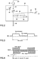
- FIG. 1 is a sectional view schematically showing a plasma etching apparatus according to the first embodiment of the present invention.
- This plasma etching apparatus is structured as a parallel-plate plasma etching apparatus of the capacitive coupling type.
- the apparatus includes an essentially cylindrical chamber (process container) 10, which is made of, e.g., aluminum with an anodization-processed surface.
- the chamber 10 is protectively grounded.
- a columnar susceptor pedestal 14 is disposed on the bottom of the chamber 10 through an insulating plate 12 made of, e.g., a ceramic.
- a susceptor 16 made of, e.g., aluminum is disposed on the susceptor pedestal 14.
- the susceptor 16 is used as a lower electrode, on which a target substrate, such as a semiconductor wafer W, is placed.
- the susceptor 16 is provided with an electrostatic chuck 18 on the top, for holding the semiconductor wafer W by an electrostatic attraction force.
- the electrostatic chuck 18 comprises an electrode 20 made of a conductive film, and a pair of insulating layers or insulating sheets sandwiching the electrode 20.
- the electrode 20 is electrically connected to a direct current (DC) power supply 22.
- the semiconductor wafer W is attracted and held on the electrostatic chuck 18 by an electrostatic attraction force, e.g., a Coulomb force, generated by a DC voltage applied from the DC power supply 22.
- the susceptor pedestal 14 is provided with a cooling medium space 28 formed therein and extending therethrough in, e.g., an annular direction.
- a cooling medium set at a predetermined temperature such as cooling water, is circulated within the cooling medium space 28 from a chiller unit (not shown) disposed outside through lines 30a and 30b.
- the temperature of the cooling medium is set to control the process temperature of the semiconductor wafer W placed on the susceptor 16.
- a heat transmission gas such as He gas
- a heat transmission gas supply unit not shown
- a gas supply line 32 is supplied from a heat transmission gas supply unit (not shown), through a gas supply line 32, into the interstice between the top surface of the electrostatic chuck 18 and the back surface of the semiconductor wafer W.
- An upper electrode 34 is disposed above the lower electrode or susceptor 16 in parallel with the susceptor.
- the space between the electrodes 16 and 34 is used as a plasma generation space.
- the upper electrode 34 defines a counter surface facing the semiconductor wafer W placed on the lower electrode or susceptor 16, and thus this counter surface is in contact with plasma generation space.
- the upper electrode 34 is supported at the top of the chamber 10 by an insulating shield member 42.
- the upper electrode 34 includes an electrode plate 36 defining the counter surface opposite to the susceptor 16 and having a number of gas delivery holes 37, and an electrode support 38 detachably supporting the electrode plate 36.
- the electrode support 38 is made of a conductive material, such as aluminum with an anodization-processed surface, and has a water-cooling structure.
- the electrode plate 36 is preferably made of a conductor or semiconductor having a low resistivity and thus generating less Joule heat. Further, in order to reinforce a resist film, as described later, the electrode plate 36 is preferably made of a silicon-containing substance. In light of these, the electrode plate 36 is preferably made of silicon or SiC.
- the electrode support 38 has a gas diffusion cell 40 formed therein, which is connected to the gas delivery holes 37 through a number of gas flow channels 41 extending downward.
- the electrode support 38 has a gas feed port 62 formed therein for feeding a process gas into the gas diffusion cell 40.
- the gas feed port 62 is connected to a process gas supply source 66 through a gas supply line 64.
- the gas supply line 64 is provided with a mass-flow controller (MFC) 68 and a switching valve 70 disposed thereon in this order from the upstream (an FCN may be used in place of the MFC).
- a process gas for etching such as a fluorocarbon gas (C x F y ), e.g., C 4 F 8 gas, is supplied from the process gas supply source 66 through the gas supply line 64 into the gas diffusion cell 40.
- the process gas flows through the gas flow channels 41 and is delivered from the gas delivery holes 37 into the plasma generation space, as in a shower device. Accordingly, in other words, the upper electrode 34 functions as a showerhead for supplying a process gas.
- the upper electrode 34 is electrically connected to a first RF power supply 48 through a first matching unit 46 and a feed rod 44.
- the first RF power supply 48 outputs an RF power with a frequency of 27 to 100 MHz, such as 60 MHz.
- the first matching unit 46 is arranged to match the load impedance with the internal (or output) impedance of the first RF power supply 48.
- the matching unit 44 performs control for the load impedance and the output impedance of the first RF power supply 48 to apparently agree with each other.
- the output terminal of the first matching unit 46 is connected to the top of the feed rod 44.
- the upper electrode 34 is electrically connected to a variable DC power supply 50 in addition to the first RF power supply 48.
- the variable DC power supply 50 may be formed of a bipolar power supply.
- the variable DC power supply 50 is connected to the upper electrode 34 through the first matching unit 46 and feed rod 44, and the electric feeding can be set on/off by an on/off switch 52.
- the polarity, current, and voltage of the variable DC power supply 50, and the on/off of the on/off switch 52 are controlled by a controller 51.
- the first matching unit 46 includes a first variable capacitor 54 disposed on a line branched from a feed line 49 of the first RF power supply 48, and a second variable capacitor 56 disposed on the feed line 49 downstream from the branch point, so as to exercise the function described above.
- the first matching unit 46 also includes a filter 58 configured to trap the RF power (of 60 MHz, for example) from the first RF power supply 48 and the RF power (of 2 MHz, for example) from a second RF power supply described later, so that a DC voltage current (which will be simply referred to as a DC voltage) is effectively supplied to the upper electrode 34. Consequently, a DC current is connected from the variable DC power supply 50 through the filter 58 to the feed line 49.
- the filter 58 is formed of a coil 59 and a capacitor 60 arranged to trap the RF power from the first RF power supply 48 and the RF power from the second RF power supply described later.
- the sidewall of the chamber 10 extends upward above the height level of the upper electrode 34 and forms a cylindrical grounded conductive body 10a.
- the top wall of the cylindrical grounded conductive body 10a is electrically insulated from the upper feed rod 44 by a tube-like insulating member 44a.
- the susceptor 16 used as a lower electrode is electrically connected to a second RF power supply 90 through a second matching unit 88.
- the RF power supplied from the second RF power supply 90 to the lower electrode or susceptor 16 is used for applying a bias to the semiconductor wafer W, thereby attracting ions toward the semiconductor wafer W.
- the second RF power supply 90 outputs an RF power with a frequency of 400 kHz to 13.56 MHz, such as 2 MHz.
- the second RF power supply 90 is connected to an RF controller 95 for controlling the second RF power supply 90.
- the RF controller 95 can control the RF power from the second RF power supply 90 to perform power modulation between first and second powers in predetermined cycles, so that modes can be switched between an ordinary continuous mode and a power control mode.
- the first power is set to generate deposition on an etching target film on the semiconductor wafer W, while the second power is set to promote etching on the etching target film on the semiconductor wafer W.
- a typical example of the power modulation is pulse-wise, as shown in FIG. 3 , but this is not limiting. In this example, the duty ratio of pulses is 50%.
- FIG. 4 shows the output voltage waveform obtained in this case. The difference between the maximum voltage value and minimum voltage value in one cycle is expressed by VPP. In FIG. 4 , Pset denotes a set voltage.
- the RF controller 95 is also connected to the second matching unit 88 to control the second matching unit 88.
- the RF controller 95 is further connected to the first RF power supply 48 and first matching unit 46 to control these members.
- the second matching unit 88 is arranged to match the load impedance with the internal (or output) impedance of the second RF power supply 90.
- the second matching unit 88 performs control for the load impedance including the plasma within the chamber 10 and the internal impedance of the second RF power supply 90 to apparently agree with each other.
- the second matching unit 88 includes a first variable capacitor 97 disposed on a line branched from the electric feeding line 96 of the second RF power supply 90, a second variable capacitor 98 disposed on the electric feeding line 96 between the branch point and second RF power supply 90, and a coil 99 disposed on the electric feeding line on the other side of the branch point.
- the RF power of the second RF power supply 90 is operated in a power modulation mode that executes power modulation in predetermined cycles.
- the RF controller 95 controls the matching operation of the second matching unit 88 to be switched in synchronism with the power modulation.
- the RF controller 95 controls the second matching unit 88, as follows. Specifically, when the first power is applied, the second matching unit 88 is controlled not to operate.
- the second matching unit 88 is controlled to operate for the load impedance including plasma within the chamber 10 and the internal impedance of the second RF power supply 90 to agree with each other. More specifically, only when the high-power-level second power is applied, the capacitance C1 of the first variable capacitor 97 and the capacitance C2 of the second variable capacitor 98 are controlled independently of each other. When the first power is applied, the capacitance C1 and capacitance C2 are fixed. In this case, if the forward direction power Pf is solely controlled as in ordinary matching units, hunching is caused.
- the second RF power supply 90 is controlled to keep the power value PL always constant.
- the first RF power supply 46 receives some influence of power modulation made on the RF power from the second RF power supply 90, so the first RF power supply 46 is also preferably provided with a matching unit including load power control, thereby performing control in the same way.
- the upper electrode 34 is electrically connected to a low-pass filter (LPF) 92, which prevents the RF power (60 MHz) from the first RF power supply 48 from passing through, while it allows the RF power (2 MHz) from the second RF power supply 98 to pass through to ground.
- the low-pass filter (LPF) 92 is preferably formed of an LR filter or LC filter, but merely one conductive line may be used for the same purpose, because it can apply a sufficiently large reactance to the RF power (60 MHz) from the first RF power supply 48.
- the lower electrode or susceptor 16 is electrically connected to a high-pass filter (HPF) 94, which allows the RF power (60 MHz) from the first RF power supply 48 to pass through to ground.
- HPF high-pass filter
- An exhaust port 80 is formed at the bottom of the chamber 10, and is connected to an exhaust unit 84 through an exhaust line 82.
- the exhaust unit 84 includes a vacuum pump, such as a turbo molecular pump, to decrease the pressure inside the chamber 10 to a predetermined vacuum level.
- a transfer port 85 for a semiconductor wafer W is formed in the sidewall of the chamber 10, and is opened/closed by a gate valve 86 attached thereon.
- a deposition shield 11 is detachably disposed along the inner wall of the chamber 10 to prevent etching by-products (deposition) from being deposited on the wall. In other words, the deposition shield 11 constitutes a chamber wall.
- a deposition shield 11 is also disposed around the inner wall member 26.
- An exhaust plate 83 is disposed at the bottom of the chamber 10 between the deposition shield 11 on the chamber wall and the deposition shield 11 on the inner wall member 26.
- the deposition shield 11 and exhaust plate 83 are preferably made of an aluminum body covered with a ceramic, such as Y 2 O 3 .
- a conductive member (GND block) 91 is disposed on a portion of the deposition shield 11 that constitutes the chamber inner wall, at a height essentially the same as the wafer W, and is connected to ground in the sense of DC. This arrangement provides the effect of preventing abnormal electric discharge, as described later.
- the position of the conductive member 91 is not limited to that shown in FIG. 1 , as long as it is inside the plasma generation area.
- the conductive member 91 may be disposed on the susceptor 16 side, such as the periphery of the susceptor 16, or it may be disposed near the upper electrode, such as a position around the upper electrode 34, in the form of a ring.
- Respective components of the plasma processing apparatus are connected to and controlled by a control section (overall control unit) 100.
- the control section 100 is connected to a user interface 101 including, e.g., a key board and a display, wherein the key board is used for a process operator to input commands for operating the plasma processing apparatus, and the display is used for showing visualized images of the operational status of the plasma processing apparatus.
- control section 100 is connected to a storage section 102 that stores control programs for the control section 100 to control the plasma processing apparatus so as to perform various processes, and programs or recipes for respective components of the plasma processing apparatus to perform processes in accordance with process conditions.
- Recipes are stored in a storage medium of the storage section 102.
- the storage medium may be a hard disk or semiconductor memory, or it may be a portable storage medium, such as a CDROM, DVD, or flash memory.
- recipes may be utilized on-line, while it is transmitted from another apparatus through, e.g., a dedicated line, as needed.
- each of the plasma processing apparatuses includes such a control section 100.
- the gate valve 86 is first opened, and a semiconductor wafer W to be etched is transferred through the transfer port 85 into the chamber 10 and placed on the susceptor 16. Then, a process gas for etching is supplied from the process gas supply source 66 into the gas diffusion cell 40 at a predetermined flow rate, and then supplied into the chamber 10 through the gas flow channels 41 and gas delivery holes 37. At the same time, the interior of the chamber 10 is exhausted by the exhaust unit 84 to set the pressure inside the chamber 10 at a predetermined value within a range of, e.g., 0.1 to 150 Pa.
- the process gas may be selected from various gases conventionally employed, and preferably is a gas containing a halogen element, a representative of which is a fluorocarbon gas (C x F y ), such as C 4 F 8 gas. Further, the process gas may contain another gas, such as Ar gas or O 2 gas.
- a gas containing a halogen element a representative of which is a fluorocarbon gas (C x F y ), such as C 4 F 8 gas.
- the process gas may contain another gas, such as Ar gas or O 2 gas.
- an RF power for plasma generation is applied from the first RF power supply 48 to the upper electrode 34.
- an RF power for ion attraction is applied from the second RF power supply 90 to the lower electrode or susceptor 16.
- a predetermined DC voltage is applied from the variable DC power supply 50 to upper electrode 34.
- a DC voltage is applied from the DC power supply 22 for the electrostatic chuck 18 to the electrode 20 of the electrostatic chuck 18 to fix the semiconductor wafer W by the electrostatic chuck 18.
- the process gas delivered from the gas delivery holes 37 formed in the electrode plate 36 of the upper electrode 34 is turned into plasma by glow discharge caused by the RF power applied across the upper electrode 34 and the lower electrode or susceptor 16. Radicals and ions generated in this plasma are used to etch the target surface of the semiconductor wafer W. As described above, a first RF power for plasma generation is applied to the upper electrode 34, and a second RF power for ion attraction is applied to the lower electrode or susceptor 16. Consequently, the plasma control margin can be set broader.
- the upper electrode 34 when plasma is generated, the upper electrode 34 is supplied with an RF power within a range covering high frequencies of 27 MHz or more. Consequently, the plasma density is increased with a preferable state, so that high density plasma is generated even under a low pressure condition.
- the controller 51 controls the polarity and value of the DC voltage applied from the variable DC power supply 50 to the upper electrode 34.
- the application electrode or upper electrode 34 is set to have a self bias voltage V dc on the surface, at a deep level for obtaining a predetermined (moderate) sputtering effect onto the surface, i.e., the surface of the electrode plate 36. In other words, control is performed to increase the absolute value of V dc on the surface of the upper electrode 34.
- the RF power applied from the first RF power supply 48 is low, polymers are deposited on the upper electrode 34.
- the application current or application power may be controlled in place of the application voltage from the variable DC power supply 50.
- etching may be performed on an etching target film formed of an SiOC family Low-k film with an underlying etching-stopper film formed of an SiC film that is a low dielectric constant barrier film. In this case, their compositions are very similar, and thus the conditional margin for ensuring a sufficient etching selectivity between them is very narrow even where a DC voltage is applied.
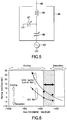
- FIG. 6 is a graph showing etching characteristics of an SiOC family Low-k film and an SiC film, wherein the horizontal axis denotes the self bias voltage V dc of a bias RF power (13.56 MHz) applied from the second RF power supply 90, and the vertical axis denotes the etching rate.
- the process gas was C 4 F 8 /Ar/N 2 set at flow rates of 10 mL/min (sccm), 500 mL/min (sccm), and 100 mL/min (sccm), respectively, and at a pressure of 6 Pa.
- the first RF power supply 48 was set to apply an RF power with a frequency of 60 MHz at 1,000W
- the second RF power supply 90 was set to apply an RF power with a frequency of 13.56 MHz at 2,000W.
- V dc is preferably set such that the SiOC family Low-k film is etched while the underlying SiC film is not etched.
- the compositions of the SiOC family Low-k film and SiC film are close to each other, and thus their etching behaviors are similar, as shown in FIG. 6 .
- ordinary etching can provide only a very narrow margin for performing etching with a high selectivity, and thus can hardly allow the etching rate to be increased.
- V dc ion energy incident on the wafer
- the polymer thickness on the underlying film is smaller than the ion penetration depth when the etching target film is penetrated, and thus the underlying film is eroded.
- this embodiment adopts control to set the polymer thickness to be larger than the ion penetration depth when the etching target film is penetrated, i.e., at the timing of transition from etching of the etching target film to over etching.
- This control is made by power modulation performed in predetermined cycles between a first power set to deposit polymers on the etching target film and a second power set to etch the etching target film on the target substrate.
- the RF controller 95 switches the second RF power supply 90 from a normal mode to a power modulation mode.
- the first power is used to deposit polymers and the second power is used to promote etching, so that the polymer layer is formed to have a lager thickness than the ion penetration depth when over etching starts, thereby stopping etching without substantially eroding the etching-stopper film.
- the following explanation is exemplified by a structure including a Cu interconnection line layer 201, on which an etching-stopper film formed of an SiC film 202 and an etching target film formed of an SiOC family Low-k film 203 are laminated in this order. Etching of the SiOC family Low-k film 203 is performed while a photo-resist film 204 is used as a mask.
- the main etching terminal state is shown in FIG. 7, (a)
- the instant when the SiOC family Low-k film 203 is penetrated (at the instant when over etching starts) is shown in FIG. 7, (b) .
- the thickness of a polymer layer 205 on the underlying SiC film 202 at the hole bottom is small, so the SiC film 202 is eroded by etching.
- the over etching is saturated (over etching of 25%).
- the mode is switched to the power modulation mode in the main etching terminal state shown in FIG. 7, (a) .
- the first power is applied so that the thickness of the polymer layer 205 on the SiC film 202 at the hole bottom is increased.
- the second power etching mode is used thereafter, the ion penetration depth is smaller than the thickness of the polymer layer 205. Consequently, as shown in FIG. 7, (f) , the etching-stopper film formed of the SiC film 202 is hardly eroded.
- FIG. 8 is a graph schematically showing the phenomenon described above, wherein the horizontal axis denotes the bias power and the vertical axis denotes the polymer layer thickness.
- FIG. 8 also shows the ion penetration depth into the polymer layer 205 or SiC film 202 (the scale is the same as that of the polymer depth).
- the etching characteristics of the SiOC family Low-k film 203 and SiC film 202 are similar, such a range is very narrow where the ion penetration depth is smaller than the thickness of the polymer layer 205 on the SiC film 202 and thus the SiC film 202 is not eroded, as described above.
- the bias power needs to be smaller to decrease the etching rate of the SiOC family Low-k film 203.
- the bias power modulation immediately before the over etching such a range is expanded where the SiC film 202 is not eroded.
- the bias power can be larger to increase the etching rate of the SiOC family Low-k film 203.
- FIG. 9 shows a process margin obtained by the case using the bias power modulation, for comparison with the case using the continuous mode shown in FIG. 6 .
- the process margin becomes broader.
- V dc is set at about -800V to perform etching at a high etching rate
- the etching target film formed of the SiOC family Low-k film can be etched with a high etching rate and high selectivity relative to the underlying film.
- FIG. 10 is a graph showing the relationship between the polymer layer depth and the absorption energy of ions (Ar ions), obtained by a simulation with different values of ion radiation energy.
- the ordinary etching is known such that the distribution of ion radiation energy is mainly formed of a range of 500 eV to 1 keV.
- an ion energy absorption range of up to 1 keV corresponds to a polymer thickness of less than about 5 nm. Accordingly, where the polymer thickness is several nm or more, and preferable 5 nm or more, the ion penetration depth becomes smaller than the polymer layer thickness.
- a pulse-wise waveform is a typical example used for power modulation performed on the RF power of the second RF power supply 90, but this is not limiting.
- another waveform such as a sine curve, may be used.
- the low-power-level first power is preferably set to be larger than 0. Where this power is set at a certain lever larger than 0, polymer deposition is effectively supplied.
- the first power and second power are suitably set in accordance with other etching conditions and/or film conditions, but the first power is preferably set to be within a range of 10 to 500W, and the second power is preferably set to be within a range of 100 to 5,000W, and more preferably of 100 to 1,000W.
- the frequency of power modulation is preferably set to be 0.25 to 100 Hz. With this range, the polymer layer is moderately generated. Specifically, it is assumed that the power modulation (pulse) has a duty ratio of 50%. In this case, if the frequency is larger than 100 Hz, the time of the first power for generating polymer deposition is less than 10 mS in one cycle, so it may be difficult to generate sufficient deposition. If the frequency is less than 0.25Hz, the time of the first power is larger than 2S in one cycle, so the thickness of the polymer layer may be too large.
- the duty ratio (second power time/one cycle total time) of the power modulation (pulse) is typically exemplified by 50%. However, the duty ratio may be suitably adjusted within a range of 1 to 99%, in accordance with etching conditions and/or conditions of the etching target film and underlying film.
- the etching target film is first etched at a high etching rate in a normal mode using no bias power modulation.
- the bias power is switched into the power modulation mode described above. This switching needs to be made at a timing such that a suitable amount of polymer layer is formed on the underlying film when the underlying film is making an appearance due to etching of the etching target film. If the switching into the power modulation mode is made immediately before over etching, the polymer layer thickness is insufficient for the over etching. On the other hand, this switching is made too early, the etching rate is decreased.
- the switching is preferably made at a timing very close to the instant when the over etching starts. Although it depends on etching conditions, the switching is preferably made at a timing when the remaining of the etching target film has a thickness of 20 to 30 nm.
- a DC voltage is applied from the variable DC power supply 50 to the upper electrode 34.
- This is advantageous to ensure the presence of a polymer layer, because the polymer supply effect can be obtained, as described above.
- no DC voltage is applied, reflected waves are increased due to the bias power modulation, in the RF power for plasma generation applied from the first RF power supply to the upper electrode 34, thereby making plasma unstable.
- a DC voltage is applied from the variable DC power supply 50 to the upper electrode 34, so that the thickness of a plasma sheath formed on the upper electrode 34 side is fixed. In this case, reflected waves are decreased in the RF power for plasma generation applied to the upper electrode 34, thereby making plasma stable. Consequently, the process stability and the service life of the first RF power supply 48 are improved. This is another reason as to why the DC voltage application is advantageous.
- the DC voltage applied to the upper electrode 34 is suitably set in accordance with etching conditions, the DC voltage is preferably set to be within a range of -300 to -2 kV in both of the ordinary continuous mode and power modulation mode.
- the frequency of the RF power applied from the first RF power supply 48 to the upper electrode 34 is preferably set to be within a range of 27 to 100 MHz in both of the ordinary continuous mode and power modulation mode.
- the frequency of the RF power applied from the second RF power supply 90 to the susceptor 16 is preferably set to be within a range of 400 kHz to 13.56 MHz in both of the ordinary continuous mode and power modulation mode.
- the power of the RF power applied from the first RF power supply 48 is preferably set to be within a range of 500 to 5,000W in both of the ordinary continuous mode and power modulation mode.
- the power of the RF power for bias applied from the second RF power supply 90 is preferably set to be within a range of 500 to 5,000W in the ordinary continuous mode.
- Samples were first prepared to each have a structure such that a 30-nm SiC film was formed as an underlying film, a 300-nm SiOC family Low-k film was formed thereon as an etching target film, and a BARC (anti-reflection coating) and a patterned ArF resist film were then formed thereon. Then, the BARC was etched by use of the ArF resist film as a mask, and the SiOC family Low-k film is etched to form a via-hole.
- a BARC anti-reflection coating
- Etching conditions used at this time were set as follows. In one example (present example), over etching was performed by use of a bias applied in a power modulation mode according to this embodiment. In another example (comparative example), over etching was performed by use of a bias applied in a conventional continuous mode.
- each sample was immersed in 1%-HF solution for 30 sec to examine the SiC erosion amount.
- the bias power application was switched from the normal mode to the power modulation mode 30 sec before the over etching started.
- FIG. 11 shows this result.
- FIG. 11 is a graph that compares the present example and comparative example, wherein the horizontal axis denotes the over etching time and the vertical axis denotes the erosion amount (nm) of the SiC film.
- the SiC film was largely eroded by about 9 nm immediately after the over etching started.
- the SiC film was eroded by about 3 nm at the beginning, and then this erosion was essentially constant or kept saturated until over etching of 40%. Accordingly, it has been confirmed that the bias power modulation mode according to this embodiment is effective.
- the etching target film is formed of an SiOC family (organic) Low-k film, but it may be formed of an inorganic Low-k film.
- the underlying film is formed of an SiC film, but it may be formed of, e.g., a silicon nitride film (SiN).
- the etching target film formed of an SiOC family Low-k film is combined with the underlying film formed of an SiC film, but the disclosed technique may be applied to any structure that has a difficulty in ensuring the selectivity of an etching target film relative to an underlying film.
- the bias is switched from the continuous mode to power modulation mode, but the power modulation mode may be solely used as long as a sufficient etching rate is obtained.
- the following application is a case where the power modulation mode described above is utilized to increase the selectivity of an etching target film relative to a mask.
- FIG. 12 is a sectional view showing the structure of a semiconductor wafer used in this case.
- This structure includes a Low-k film 301, on which a hard mask layer formed of a TiN film 302, an inorganic sacrificial film 303, and a photo-resist film 304 are laminated in this order.
- the hard mask layer may be formed of a Ti film in place of the TiN film.
- the selectivity of the Low-k film 301 relative to the TiN film 302 is preferably larger.
- FIG. 13 shows a structure including an underlying film 401, on which an etching-stopper film formed of an SiC film 402, and an etching target film formed of an SiOC family Low-k film 403 are laminated in this order.
- the SiOC family Low-k film 403 is etched by use of a photo-resist film 404 as a mask to form a smaller size via-hole 405 and a larger area trench 406, such as a guard ring (GR).
- GR guard ring
- the etching makes progress when the high-power-level second power is applied, and the etching is suppressed due to CF family precursor deposition when the low-power-level first power is applied.
- the effect of suppressing the etching is exerted more on the larger area trench 406, so the difference in etching rate between the via-hole 405 and trench 406 is decreased, thereby alleviating the micro-loading effect.
- An etching target film formed of an SiOC family Low-k film was etched to form an elliptical via-hole, a circular small via-hole, and a trench (GR) having sizes, as shown in FIGS. 14A, 14B, and 14C , respectively.
- An example using a power modulation mode was compared with an example using a continuous mode, both modes being applied on the lower side application RF power. Conditions used at this time were set as follows.
- Table 1 shows values of the etching rate at the center and edge obtained by the etching using these modes.
- Table 2 shows values normalized by use of values of the etching rate of the elliptical via-hole shown in FIG. 14A , set as a reference value of 1.0.
- FIG. 15 shows a graph of Table 2.
- plasma is generated by use of the power modulation mode on the second RF power supply 90.
- the second RF power supply 90 is preferably operated in the continuous mode using a constant power level for plasma ignition, and then operated in the power modulation mode, to reliably maintain the plasma.
- the application timing and application manner of the RF power and DC voltage are important issues. Accordingly, preferable application timing and application manner of the RF power and DC voltage will be explained with reference to FIGS. 16 to 18 .
- the RF power applied from the second RF power supply 90 to the lower electrode or susceptor 16 is first set in a continuous mode at a power level lower than the high-power-level second power. Then, at a time point T1 when a predetermined time has elapsed, the RF power applied from the first RF power supply 48 to the upper electrode 34 is started. At the same time, the DC voltage applied from the variable DC power supply 50 to the upper electrode 34 is started. In this state, plasma is ignited, and then, at a time point T2 when the plasma becomes stable, the second RF power supply 90 is switched to the power modulation mode.
- the power applied from the second RF power supply 90 is slowly increased to the value of the high-power-level second power, and is then switched to the power modulation mode. Further, the DC voltage applied from the variable DC power supply 50 is slowly increased. Where the power and voltage are slowly increased, the wafer and/or power supplies are less damaged. Only one of the power and voltage may be slowly increased.
- the RF power applied from the second RF power supply 90 to the lower electrode or susceptor 16 is first set in a continuous mode at a power level lower than the high-power-level second power. Then, at a time point T1' when a predetermined time has elapsed, the RF power applied from the first RF power supply 48 to the upper electrode 34 is started at a power level lower than the set value. At the same time, the DC voltage applied from the variable DC power supply 50 to the upper electrode 34 is started.
- the RF power applied from the first RF power supply 48 is increased to the set value, and the RF power applied from the second RF power supply 90 is increased to a predetermined value (for example, to the value of the second power).
- the power from the second RF power supply 90 is preferably slowly increased, as shown in FIG. 18 .
- the second RF power supply 90 is switched to the power modulation mode.
- the power modulation mode since the power modulation mode is used after the plasma becomes stable, the plasma can be reliably maintained even when the low-power-level first power is supplied in the power modulation mode.
- the DC voltage applied from the variable DC power supply 50 may be slowly increased.
- the power modulation mode may be applied not only to the second RF power supply 90 but also to the first RF power supply 48. Such an example will be described below.
- the RF controller 95 is arranged to control both of the second RF power supply 90 and first RF power supply 48 to perform power modulation.
- the first RF power supply 48 is controlled to perform power modulation between a third power and a fourth power in synchronism with the power modulation mode of the second RF power supply 90.
- the first RF power supply 48 and second RF power supply 90 may be controlled to have high powers and low powers at the same timing.
- the first RF power supply 48 and second RF power supply 90 may be controlled to have high powers and low powers at opposite timing.
- FIG. 20 is a sectional view schematically showing a plasma etching apparatus according to a second embodiment of the present invention.
- This plasma etching apparatus has a structure essentially the same as that of the plasma etching apparatus according to the first embodiment except that an RF power for plasma generation is applied to the lower electrode or susceptor. Accordingly, the same constituent elements as those in FIG. 1 are denoted by the same reference numerals in FIG. 20 , and their description will be omitted.
- a lower electrode or susceptor 16 is connected to both of a first RF power supply 48' for plasma generation and a second RF power supply 90 for applying a bias for ion attraction.
- the first RF power supply 48' is connected to the susceptor 16 through a first matching unit 89.
- the first matching unit 89 has the same structure as the second matching unit 88, and, when plasma is generated within a chamber 10, it performs control for the load impedance and the output impedance of the first RF power supply 48' to apparently agree with each other.
- the first RF power supply 48' has the same function as the first RF power supply 48 of the first embodiment, and preferably has a frequency within a range of 27 to 100 MHz.
- the upper electrode 34 is not connected to any RF power supply, but is connected to a variable DC power supply 50 through a low-pass filter (LPF) 46a.
- the low-pass filter (LPF) 46a is arranged to trap the RF powers from the first and second RF power supplies, and is preferably formed of an LR filter or LC filter
- the plasma etching apparatus is of the type that applies two RF powers with different frequencies to the lower side, i.e., a first radio frequency (RF) power for plasma generation and a second radio frequency (RF) power for ion attraction are applied to the lower electrode.
- RF radio frequency
- This type has the following advantages, as compared to the other plasma etching apparatus of the capacitive coupling type.
- an RF power for plasma generation is applied to the lower electrode, plasma is generated near the wafer, and dissociation of the process gas is suppressed because plasma is prevented from widely diffusing. Consequently, even where the pressure inside the process container is high and the plasma density is low, the etching rate on the wafer can be increased. Further, even where the RF power for plasma generation has a high frequency, it is possible to ensure relatively large ion energy and thus attain a high efficiency. By contrast, where an RF power for plasma generation is applied to the upper electrode as in the first embodiment, plasma is generated near the upper electrode. In this case, it is relatively difficult to increase the etching rate on the wafer, if the pressure inside the process container is high and the plasma density is low.
- a DC voltage is applied to the upper electrode, so that additional functions are obtained, as described above. Consequently, it is possible to provide high performance etching, which is more suitable for recent etching micro-fabrication.
- the bias RF power modulation is used in the same way as the first embodiment, so that the etching target film can be etched with a high selectivity and a high etching rate, even where the compositions of the etching target film and underlying film are similar, as in a combination of an SiOC family Low-k film and an SiC film.
- This embodiment may be utilized to increase the selectivity of an etching target film relative to an underlying film, as in a case where an SiOC film is etched on an underlying SiC film; to increase the selectivity of an etching target film relative to a mask, as in a case where a Low-k film is etched by use of a TiN film as a mask; or to alleviate the micro-loading effect, as in the first embodiment.
- the plasma ignition sequence shown in each of FIGS. 16 to 18 may be used, and/or the first RF power supply 48' may be operated in the power modulation mode.
- the etching target film is an SiOC family (organic) Low-k film, but it may be formed of an inorganic Low-k film.
- the underlying film is formed of an SiC film, but it may be formed of, e.g., a silicon nitride film (SiN). Further, in this embodiment, the etching target film formed of an SiOC family Low-k film is combined with the underlying film formed of an SiC film, but the disclosed technique may be applied to any structure that has a difficulty in ensuring the selectivity of an etching target film relative to an underlying film.
- the first RF power and second RF power may have frequencies, as follows.
- the frequency of the first RF power may be one of 27 MHz, 40 MHz, 60 MHz, 80 MHz, and 100 MHz
- the frequency of the second RF power may be one of 400 kHz, 800 kHz, 1 MHz, 2 MHz, 3.2 MHz, 12.88 MHz, and 13.56 MHz. They are suitably combined in accordance with a process to be performed.
Landscapes
- Engineering & Computer Science (AREA)
- Physics & Mathematics (AREA)
- Chemical & Material Sciences (AREA)
- Plasma & Fusion (AREA)
- Analytical Chemistry (AREA)
- Computer Hardware Design (AREA)
- General Physics & Mathematics (AREA)
- Manufacturing & Machinery (AREA)
- Condensed Matter Physics & Semiconductors (AREA)
- Microelectronics & Electronic Packaging (AREA)
- Power Engineering (AREA)
- Chemical Kinetics & Catalysis (AREA)
- General Chemical & Material Sciences (AREA)
- Inorganic Chemistry (AREA)
- Drying Of Semiconductors (AREA)
- Plasma Technology (AREA)
Priority Applications (2)
| Application Number | Priority Date | Filing Date | Title |
|---|---|---|---|
| EP19208518.1A EP3654367A1 (en) | 2006-10-06 | 2007-10-05 | Plasma etching apparatus |
| EP17160784.9A EP3200220B1 (en) | 2006-10-06 | 2007-10-05 | Plasma etching apparatus and plasma etching method |
Applications Claiming Priority (4)
| Application Number | Priority Date | Filing Date | Title |
|---|---|---|---|
| JP2006275722 | 2006-10-06 | ||
| JP2007164637 | 2007-06-22 | ||
| JP2007254058A JP5192209B2 (ja) | 2006-10-06 | 2007-09-28 | プラズマエッチング装置、プラズマエッチング方法およびコンピュータ読取可能な記憶媒体 |
| PCT/JP2007/069563 WO2008044633A1 (fr) | 2006-10-06 | 2007-10-05 | Dispositif et procédé de gravure au plasma |
Related Child Applications (3)
| Application Number | Title | Priority Date | Filing Date |
|---|---|---|---|
| EP17160784.9A Division EP3200220B1 (en) | 2006-10-06 | 2007-10-05 | Plasma etching apparatus and plasma etching method |
| EP17160784.9A Division-Into EP3200220B1 (en) | 2006-10-06 | 2007-10-05 | Plasma etching apparatus and plasma etching method |
| EP19208518.1A Division EP3654367A1 (en) | 2006-10-06 | 2007-10-05 | Plasma etching apparatus |
Publications (3)
| Publication Number | Publication Date |
|---|---|
| EP2068353A1 EP2068353A1 (en) | 2009-06-10 |
| EP2068353A4 EP2068353A4 (en) | 2011-01-12 |
| EP2068353B1 true EP2068353B1 (en) | 2017-05-31 |
Family
ID=39282829
Family Applications (3)
| Application Number | Title | Priority Date | Filing Date |
|---|---|---|---|
| EP07829301.6A Not-in-force EP2068353B1 (en) | 2006-10-06 | 2007-10-05 | Plasma etching device and plasma etching method |
| EP17160784.9A Active EP3200220B1 (en) | 2006-10-06 | 2007-10-05 | Plasma etching apparatus and plasma etching method |
| EP19208518.1A Withdrawn EP3654367A1 (en) | 2006-10-06 | 2007-10-05 | Plasma etching apparatus |
Family Applications After (2)
| Application Number | Title | Priority Date | Filing Date |
|---|---|---|---|
| EP17160784.9A Active EP3200220B1 (en) | 2006-10-06 | 2007-10-05 | Plasma etching apparatus and plasma etching method |
| EP19208518.1A Withdrawn EP3654367A1 (en) | 2006-10-06 | 2007-10-05 | Plasma etching apparatus |
Country Status (7)
| Country | Link |
|---|---|
| US (3) | US8852385B2 (enExample) |
| EP (3) | EP2068353B1 (enExample) |
| JP (1) | JP5192209B2 (enExample) |
| KR (1) | KR101154559B1 (enExample) |
| CN (1) | CN101523569B (enExample) |
| TW (1) | TWI509684B (enExample) |
| WO (1) | WO2008044633A1 (enExample) |
Families Citing this family (79)
| Publication number | Priority date | Publication date | Assignee | Title |
|---|---|---|---|---|
| KR100801711B1 (ko) * | 2007-02-27 | 2008-02-11 | 삼성전자주식회사 | 반도체 식각 및 증착 공정들을 수행하는 반도체 제조장비들 및 그를 이용한 반도체 소자의 형성방법들 |
| JP5390846B2 (ja) * | 2008-12-09 | 2014-01-15 | 東京エレクトロン株式会社 | プラズマエッチング装置及びプラズマクリーニング方法 |
| JP2010161156A (ja) * | 2009-01-07 | 2010-07-22 | Tokyo Electron Ltd | プラズマエッチング方法 |
| JP5466480B2 (ja) * | 2009-02-20 | 2014-04-09 | 東京エレクトロン株式会社 | プラズマエッチング方法、プラズマエッチング装置および記憶媒体 |
| JP2010205967A (ja) * | 2009-03-04 | 2010-09-16 | Tokyo Electron Ltd | プラズマエッチング方法、プラズマエッチング装置及びコンピュータ記憶媒体 |
| JP2010238881A (ja) | 2009-03-31 | 2010-10-21 | Tokyo Electron Ltd | プラズマ処理装置及びプラズマ処理方法 |
| JP5395491B2 (ja) * | 2009-03-31 | 2014-01-22 | 東京エレクトロン株式会社 | 基板処理装置及び基板処理方法 |
| US8404598B2 (en) * | 2009-08-07 | 2013-03-26 | Applied Materials, Inc. | Synchronized radio frequency pulsing for plasma etching |
| KR101286242B1 (ko) * | 2009-12-14 | 2013-07-15 | 삼성전자주식회사 | 반도체 소자 제조 방법 |
| US9373521B2 (en) | 2010-02-24 | 2016-06-21 | Tokyo Electron Limited | Etching processing method |
| JP5662079B2 (ja) * | 2010-02-24 | 2015-01-28 | 東京エレクトロン株式会社 | エッチング処理方法 |
| JP5709505B2 (ja) * | 2010-12-15 | 2015-04-30 | 東京エレクトロン株式会社 | プラズマ処理装置、プラズマ処理方法、および記憶媒体 |
| DE102011004581A1 (de) | 2011-02-23 | 2012-08-23 | Globalfoundries Dresden Module One Limited Liability Company & Co. Kg | Technik zur Reduzierung der plasmahervorgerufenen Ätzschäden während der Herstellung von Kontaktdurchführungen in Zwischenschichtdielektrika durch modifizierten HF-Leistungshochlauf |
| US20120302065A1 (en) * | 2011-05-26 | 2012-11-29 | Nanya Technology Corporation | Pulse-plasma etching method and pulse-plasma etching apparatus |
| KR101851005B1 (ko) | 2011-06-02 | 2018-04-20 | 에스케이하이닉스 주식회사 | 플라즈마 도핑 장치를 이용한 플라즈마 도핑 방법 |
| CN102281698A (zh) * | 2011-07-19 | 2011-12-14 | 大连理工大学 | 一种用脉冲调制改善等离子体特性的方法 |
| TWI500066B (zh) * | 2011-07-27 | 2015-09-11 | Hitachi High Tech Corp | Plasma processing device |
| US8735291B2 (en) | 2011-08-25 | 2014-05-27 | Tokyo Electron Limited | Method for etching high-k dielectric using pulsed bias power |
| CN103035466B (zh) * | 2011-10-08 | 2016-06-08 | 北京北方微电子基地设备工艺研究中心有限责任公司 | 一种预清洗方法及等离子体设备 |
| US9666414B2 (en) * | 2011-10-27 | 2017-05-30 | Applied Materials, Inc. | Process chamber for etching low k and other dielectric films |
| JP5977509B2 (ja) | 2011-12-09 | 2016-08-24 | 東京エレクトロン株式会社 | プラズマ処理方法及びプラズマ処理装置 |
| JP5867701B2 (ja) | 2011-12-15 | 2016-02-24 | 東京エレクトロン株式会社 | プラズマ処理装置 |
| JP5808012B2 (ja) | 2011-12-27 | 2015-11-10 | 東京エレクトロン株式会社 | プラズマ処理装置 |
| KR102034556B1 (ko) * | 2012-02-09 | 2019-10-21 | 도쿄엘렉트론가부시키가이샤 | 플라즈마 처리 방법 |
| US9698386B2 (en) | 2012-04-13 | 2017-07-04 | Oti Lumionics Inc. | Functionalization of a substrate |
| US8853070B2 (en) * | 2012-04-13 | 2014-10-07 | Oti Lumionics Inc. | Functionalization of a substrate |
| JP6002556B2 (ja) * | 2012-11-27 | 2016-10-05 | 株式会社日立ハイテクノロジーズ | プラズマ処理装置およびプラズマ処理方法 |
| CN103887146B (zh) * | 2012-12-19 | 2016-08-31 | 中微半导体设备(上海)有限公司 | 利用可切换功率发生器的高深宽比微结构刻蚀方法 |
| US8668835B1 (en) | 2013-01-23 | 2014-03-11 | Lam Research Corporation | Method of etching self-aligned vias and trenches in a multi-layer film stack |
| JP6267989B2 (ja) * | 2013-02-18 | 2018-01-24 | 東京エレクトロン株式会社 | プラズマ処理方法及び容量結合型プラズマ処理装置 |
| US20140262031A1 (en) * | 2013-03-12 | 2014-09-18 | Sergey G. BELOSTOTSKIY | Multi-mode etch chamber source assembly |
| JP6037914B2 (ja) * | 2013-03-29 | 2016-12-07 | 富士フイルム株式会社 | 保護膜のエッチング方法およびテンプレートの製造方法 |
| US8906810B2 (en) | 2013-05-07 | 2014-12-09 | Lam Research Corporation | Pulsed dielectric etch process for in-situ metal hard mask shape control to enable void-free metallization |
| JP6180799B2 (ja) * | 2013-06-06 | 2017-08-16 | 株式会社日立ハイテクノロジーズ | プラズマ処理装置 |
| US9401263B2 (en) * | 2013-09-19 | 2016-07-26 | Globalfoundries Inc. | Feature etching using varying supply of power pulses |
| JP5701958B2 (ja) * | 2013-10-15 | 2015-04-15 | 東京エレクトロン株式会社 | 基板処理装置 |
| DE102014209469A1 (de) * | 2014-05-19 | 2015-11-19 | TRUMPF Hüttinger GmbH + Co. KG | Regelungsanordnung, Regelsystem und Hochfrequenzleistungserzeugungsvorrichtung |
| JP6327970B2 (ja) * | 2014-06-19 | 2018-05-23 | 東京エレクトロン株式会社 | 絶縁膜をエッチングする方法 |
| US20160020119A1 (en) * | 2014-07-16 | 2016-01-21 | Macronix International Co., Ltd. | Method of Controlling Recess Depth and Bottom ECD in Over-Etching |
| JP6315809B2 (ja) * | 2014-08-28 | 2018-04-25 | 東京エレクトロン株式会社 | エッチング方法 |
| JP6316735B2 (ja) * | 2014-12-04 | 2018-04-25 | 東京エレクトロン株式会社 | プラズマエッチング方法 |
| JP6410592B2 (ja) * | 2014-12-18 | 2018-10-24 | 東京エレクトロン株式会社 | プラズマエッチング方法 |
| JP6558901B2 (ja) * | 2015-01-06 | 2019-08-14 | 東京エレクトロン株式会社 | プラズマ処理方法 |
| US9779919B2 (en) * | 2015-01-09 | 2017-10-03 | Hitachi High-Technologies Corporation | Plasma processing apparatus and plasma processing method |
| US10153139B2 (en) * | 2015-06-17 | 2018-12-11 | Applied Materials, Inc. | Multiple electrode substrate support assembly and phase control system |
| JP6552346B2 (ja) * | 2015-09-04 | 2019-07-31 | 東京エレクトロン株式会社 | 基板処理装置 |
| US9978606B2 (en) * | 2015-10-02 | 2018-05-22 | Applied Materials, Inc. | Methods for atomic level resolution and plasma processing control |
| JP6498152B2 (ja) * | 2015-12-18 | 2019-04-10 | 東京エレクトロン株式会社 | エッチング方法 |
| US10340123B2 (en) * | 2016-05-26 | 2019-07-02 | Tokyo Electron Limited | Multi-frequency power modulation for etching high aspect ratio features |
| US11004660B2 (en) | 2018-11-30 | 2021-05-11 | Eagle Harbor Technologies, Inc. | Variable output impedance RF generator |
| JP6770868B2 (ja) | 2016-10-26 | 2020-10-21 | 東京エレクトロン株式会社 | プラズマ処理装置のインピーダンス整合のための方法 |
| US10818502B2 (en) * | 2016-11-21 | 2020-10-27 | Tokyo Electron Limited | System and method of plasma discharge ignition to reduce surface particles |
| JP7017306B2 (ja) * | 2016-11-29 | 2022-02-08 | 株式会社日立ハイテク | 真空処理装置 |
| US10847368B2 (en) * | 2017-04-07 | 2020-11-24 | Applied Materials, Inc. | EUV resist patterning using pulsed plasma |
| JP6688763B2 (ja) * | 2017-05-30 | 2020-04-28 | 東京エレクトロン株式会社 | プラズマ処理方法 |
| JP6878154B2 (ja) * | 2017-06-05 | 2021-05-26 | 東京エレクトロン株式会社 | エッチング方法およびエッチング装置 |
| KR102435263B1 (ko) * | 2017-07-25 | 2022-08-23 | 삼성전자주식회사 | 플라즈마 처리 장치 및 방법, 및 이를 이용한 반도체 장치의 제조 방법 |
| KR20190014623A (ko) * | 2017-08-03 | 2019-02-13 | 삼성전자주식회사 | 플라즈마 공정 장치 및 이를 이용한 반도체 장치 제조 방법 |
| KR102550393B1 (ko) | 2017-10-25 | 2023-06-30 | 삼성전자주식회사 | 플라즈마 처리 장치 및 이를 이용한 반도체 장치의 제조 방법 |
| JP6886940B2 (ja) * | 2018-04-23 | 2021-06-16 | 東京エレクトロン株式会社 | プラズマ処理方法 |
| JP6846387B2 (ja) | 2018-06-22 | 2021-03-24 | 東京エレクトロン株式会社 | プラズマ処理方法及びプラズマ処理装置 |
| JP7306886B2 (ja) * | 2018-07-30 | 2023-07-11 | 東京エレクトロン株式会社 | 制御方法及びプラズマ処理装置 |
| CN110858530B (zh) * | 2018-08-24 | 2023-04-14 | 北京北方华创微电子装备有限公司 | 匹配网络、阻抗匹配器以及阻抗匹配方法 |
| US12456604B2 (en) | 2019-12-24 | 2025-10-28 | Eagle Harbor Technologies, Inc. | Nanosecond pulser RF isolation for plasma systems |
| JP7345382B2 (ja) * | 2018-12-28 | 2023-09-15 | 東京エレクトロン株式会社 | プラズマ処理装置及び制御方法 |
| JP7061981B2 (ja) * | 2019-03-28 | 2022-05-02 | 東京エレクトロン株式会社 | プラズマエッチング装置およびプラズマエッチング方法 |
| JP7514913B2 (ja) * | 2019-08-01 | 2024-07-11 | ラム リサーチ コーポレーション | エッジリングポケットを洗浄するためのシステムおよび方法 |
| US11545341B2 (en) | 2019-10-02 | 2023-01-03 | Samsung Electronics Co., Ltd. | Plasma etching method and semiconductor device fabrication method including the same |
| JP7433271B2 (ja) * | 2020-04-27 | 2024-02-19 | 東京エレクトロン株式会社 | 基板処理装置および基板処理装置の制御方法 |
| KR20220027803A (ko) * | 2020-08-27 | 2022-03-08 | 주식회사 히타치하이테크 | 플라스마 처리 장치 |
| CN114695051B (zh) * | 2020-12-31 | 2025-02-21 | 拓荆科技股份有限公司 | 半导体处理设备及方法 |
| WO2022168642A1 (ja) * | 2021-02-04 | 2022-08-11 | 東京エレクトロン株式会社 | プラズマ処理装置及びプラズマ処理方法 |
| US12300467B2 (en) * | 2021-05-20 | 2025-05-13 | Tokyo Electron Limited | Plasma processing method and plasma processing apparatus |
| JP7036999B1 (ja) * | 2021-07-16 | 2022-03-15 | 株式会社アルバック | 成膜方法及び成膜装置 |
| US12002663B2 (en) * | 2021-07-16 | 2024-06-04 | Taiwan Semiconductor Manufacturing Company, Ltd. | Processing apparatus and method for forming semiconductor structure |
| CN114063479B (zh) * | 2021-11-12 | 2024-01-23 | 华科电子股份有限公司 | 应用于蚀刻机的多路输出模块的射频电源控制方法及系统 |
| TW202410119A (zh) | 2022-04-25 | 2024-03-01 | 日商東京威力科創股份有限公司 | 電漿處理裝置、電源系統及電漿處理方法 |
| CN115050625B (zh) * | 2022-05-30 | 2025-03-14 | 北京北方华创微电子装备有限公司 | 半导体工艺腔室及其清洗方法 |
| CN115863131A (zh) * | 2022-11-18 | 2023-03-28 | 无锡尚积半导体科技有限公司 | 一种刻蚀装置 |
Family Cites Families (40)
| Publication number | Priority date | Publication date | Assignee | Title |
|---|---|---|---|---|
| US4263088A (en) * | 1979-06-25 | 1981-04-21 | Motorola, Inc. | Method for process control of a plasma reaction |
| KR900007687B1 (ko) * | 1986-10-17 | 1990-10-18 | 가부시기가이샤 히다찌세이사꾸쇼 | 플라즈마처리방법 및 장치 |
| JP2728010B2 (ja) | 1995-03-15 | 1998-03-18 | 株式会社日立製作所 | プラズマ処理方法 |
| JP3122618B2 (ja) * | 1996-08-23 | 2001-01-09 | 東京エレクトロン株式会社 | プラズマ処理装置 |
| JP3629705B2 (ja) | 1997-06-06 | 2005-03-16 | 東京エレクトロン株式会社 | プラズマ処理装置 |
| JPH113879A (ja) | 1997-06-11 | 1999-01-06 | Hitachi Ltd | 表面処理装置およびその運転方法 |
| US6200651B1 (en) * | 1997-06-30 | 2001-03-13 | Lam Research Corporation | Method of chemical vapor deposition in a vacuum plasma processor responsive to a pulsed microwave source |
| US6093332A (en) * | 1998-02-04 | 2000-07-25 | Lam Research Corporation | Methods for reducing mask erosion during plasma etching |
| JPH11340213A (ja) | 1998-03-12 | 1999-12-10 | Hitachi Ltd | 試料の表面加工方法 |
| JP2000012524A (ja) | 1998-06-24 | 2000-01-14 | Hitachi Ltd | ドライエッチング方法 |
| KR100514150B1 (ko) * | 1998-11-04 | 2005-09-13 | 서페이스 테크놀로지 시스템스 피엘씨 | 기판 에칭 방법 및 장치 |
| JP4230029B2 (ja) | 1998-12-02 | 2009-02-25 | 東京エレクトロン株式会社 | プラズマ処理装置およびエッチング方法 |
| JP4680333B2 (ja) * | 1998-12-28 | 2011-05-11 | 東京エレクトロンAt株式会社 | プラズマ処理方法、エッチング方法、プラズマ処理装置及びエッチング装置 |
| KR100317915B1 (ko) | 1999-03-22 | 2001-12-22 | 윤종용 | 플라즈마 식각 장치 |
| JP4831853B2 (ja) * | 1999-05-11 | 2011-12-07 | 東京エレクトロン株式会社 | 容量結合型平行平板プラズマエッチング装置およびそれを用いたプラズマエッチング方法 |
| KR100327346B1 (ko) * | 1999-07-20 | 2002-03-06 | 윤종용 | 선택적 폴리머 증착을 이용한 플라즈마 식각방법 및 이를이용한 콘택홀 형성방법 |
| JP4578651B2 (ja) | 1999-09-13 | 2010-11-10 | 東京エレクトロン株式会社 | プラズマ処理方法およびプラズマ処理装置、プラズマエッチング方法 |
| JP2002110647A (ja) | 2000-09-29 | 2002-04-12 | Hitachi Ltd | 半導体集積回路装置の製造方法 |
| JP2002270586A (ja) | 2001-03-08 | 2002-09-20 | Tokyo Electron Ltd | 有機系絶縁膜のエッチング方法およびデュアルダマシンプロセス |
| WO2003021002A1 (en) * | 2001-08-29 | 2003-03-13 | Tokyo Electron Limited | Apparatus and method for plasma processing |
| DE10309711A1 (de) * | 2001-09-14 | 2004-09-16 | Robert Bosch Gmbh | Verfahren zum Einätzen von Strukturen in einem Ätzkörper mit einem Plasma |
| US6818562B2 (en) * | 2002-04-19 | 2004-11-16 | Applied Materials Inc | Method and apparatus for tuning an RF matching network in a plasma enhanced semiconductor wafer processing system |
| US7473377B2 (en) * | 2002-06-27 | 2009-01-06 | Tokyo Electron Limited | Plasma processing method |
| JP4370789B2 (ja) * | 2002-07-12 | 2009-11-25 | 東京エレクトロン株式会社 | プラズマ処理装置及び可変インピーダンス手段の校正方法 |
| US6905626B2 (en) * | 2002-07-24 | 2005-06-14 | Unaxis Usa Inc. | Notch-free etching of high aspect SOI structures using alternating deposition and etching and pulsed plasma |
| JP3844460B2 (ja) * | 2002-08-05 | 2006-11-15 | パイオニア株式会社 | 空間光変調器 |
| JP4071069B2 (ja) | 2002-08-28 | 2008-04-02 | 東京エレクトロン株式会社 | 絶縁膜のエッチング方法 |
| US6759339B1 (en) * | 2002-12-13 | 2004-07-06 | Silicon Magnetic Systems | Method for plasma etching a microelectronic topography using a pulse bias power |
| US6916746B1 (en) * | 2003-04-09 | 2005-07-12 | Lam Research Corporation | Method for plasma etching using periodic modulation of gas chemistry |
| US7976673B2 (en) * | 2003-05-06 | 2011-07-12 | Lam Research Corporation | RF pulsing of a narrow gap capacitively coupled reactor |
| US7144521B2 (en) * | 2003-08-22 | 2006-12-05 | Lam Research Corporation | High aspect ratio etch using modulation of RF powers of various frequencies |
| US20050241762A1 (en) * | 2004-04-30 | 2005-11-03 | Applied Materials, Inc. | Alternating asymmetrical plasma generation in a process chamber |
| JP4672455B2 (ja) | 2004-06-21 | 2011-04-20 | 東京エレクトロン株式会社 | プラズマエッチング装置およびプラズマエッチング方法、ならびにコンピュータ読み取り可能な記憶媒体 |
| WO2005124844A1 (ja) * | 2004-06-21 | 2005-12-29 | Tokyo Electron Limited | プラズマ処理装置及び方法 |
| US7740737B2 (en) * | 2004-06-21 | 2010-06-22 | Tokyo Electron Limited | Plasma processing apparatus and method |
| US7988816B2 (en) | 2004-06-21 | 2011-08-02 | Tokyo Electron Limited | Plasma processing apparatus and method |
| JP4640939B2 (ja) * | 2005-01-13 | 2011-03-02 | 株式会社日立ハイテクノロジーズ | プラズマ処理装置およびプラズマ処理方法 |
| JP4642528B2 (ja) * | 2005-03-31 | 2011-03-02 | 東京エレクトロン株式会社 | プラズマ処理装置およびプラズマ処理方法 |
| JP4704087B2 (ja) * | 2005-03-31 | 2011-06-15 | 東京エレクトロン株式会社 | プラズマ処理装置およびプラズマ処理方法 |
| JP4754374B2 (ja) | 2006-03-16 | 2011-08-24 | 東京エレクトロン株式会社 | プラズマエッチング方法およびコンピュータ読み取り可能な記憶媒体 |
-
2007
- 2007-09-28 JP JP2007254058A patent/JP5192209B2/ja not_active Expired - Fee Related
- 2007-10-04 US US11/867,371 patent/US8852385B2/en active Active
- 2007-10-05 KR KR1020097006959A patent/KR101154559B1/ko not_active Expired - Fee Related
- 2007-10-05 CN CN2007800369156A patent/CN101523569B/zh not_active Expired - Fee Related
- 2007-10-05 WO PCT/JP2007/069563 patent/WO2008044633A1/ja not_active Ceased
- 2007-10-05 EP EP07829301.6A patent/EP2068353B1/en not_active Not-in-force
- 2007-10-05 EP EP17160784.9A patent/EP3200220B1/en active Active
- 2007-10-05 EP EP19208518.1A patent/EP3654367A1/en not_active Withdrawn
- 2007-10-05 TW TW096137552A patent/TWI509684B/zh not_active IP Right Cessation
-
2014
- 2014-09-17 US US14/489,125 patent/US10229815B2/en active Active
-
2018
- 2018-12-21 US US16/228,960 patent/US10861678B2/en not_active Expired - Fee Related
Non-Patent Citations (1)
| Title |
|---|
| None * |
Also Published As
| Publication number | Publication date |
|---|---|
| EP2068353A4 (en) | 2011-01-12 |
| US20150000843A1 (en) | 2015-01-01 |
| TWI509684B (zh) | 2015-11-21 |
| JP2009033080A (ja) | 2009-02-12 |
| EP3200220B1 (en) | 2019-12-25 |
| KR20090057088A (ko) | 2009-06-03 |
| US20080110859A1 (en) | 2008-05-15 |
| CN101523569B (zh) | 2012-07-18 |
| EP3654367A1 (en) | 2020-05-20 |
| US10861678B2 (en) | 2020-12-08 |
| JP5192209B2 (ja) | 2013-05-08 |
| CN101523569A (zh) | 2009-09-02 |
| US20190115192A1 (en) | 2019-04-18 |
| US10229815B2 (en) | 2019-03-12 |
| US8852385B2 (en) | 2014-10-07 |
| WO2008044633A1 (fr) | 2008-04-17 |
| EP2068353A1 (en) | 2009-06-10 |
| TW200839868A (en) | 2008-10-01 |
| KR101154559B1 (ko) | 2012-06-08 |
| EP3200220A1 (en) | 2017-08-02 |
Similar Documents
| Publication | Publication Date | Title |
|---|---|---|
| US10861678B2 (en) | Plasma etching apparatus and method | |
| EP1708241B1 (en) | Capacitively coupled plasma processing apparatus and method | |
| JP5764186B2 (ja) | プラズマエッチング装置およびプラズマエッチング方法 | |
| JP4827081B2 (ja) | プラズマエッチング方法およびコンピュータ読み取り可能な記憶媒体 | |
| US9455153B2 (en) | Plasma processing method | |
| US9034198B2 (en) | Plasma etching method | |
| US8404595B2 (en) | Plasma processing method | |
| US8609547B2 (en) | Plasma etching method and computer-readable storage medium | |
| KR20050016080A (ko) | 탄소-도우핑된 저유전체들의 선택적 식각 | |
| WO2001068939A2 (en) | Magnetically enhanced plasma etch process using a heavy fluorocarbon etching gas | |
| US9418863B2 (en) | Method for etching etching target layer | |
| KR20080006457A (ko) | 플라즈마 에칭 방법 및 컴퓨터 판독 가능한 기억 매체 | |
| US7692916B2 (en) | Capacitive coupling plasma processing apparatus and method | |
| US20080014755A1 (en) | Plasma etching method and computer-readable storage medium |
Legal Events
| Date | Code | Title | Description |
|---|---|---|---|
| PUAI | Public reference made under article 153(3) epc to a published international application that has entered the european phase |
Free format text: ORIGINAL CODE: 0009012 |
|
| 17P | Request for examination filed |
Effective date: 20090320 |
|
| AK | Designated contracting states |
Kind code of ref document: A1 Designated state(s): AT BE BG CH CY CZ DE DK EE ES FI FR GB GR HU IE IS IT LI LT LU LV MC MT NL PL PT RO SE SI SK TR |
|
| AX | Request for extension of the european patent |
Extension state: AL BA HR MK RS |
|
| A4 | Supplementary search report drawn up and despatched |
Effective date: 20101214 |
|
| DAX | Request for extension of the european patent (deleted) | ||
| REG | Reference to a national code |
Ref country code: DE Ref legal event code: R079 Ref document number: 602007051186 Country of ref document: DE Free format text: PREVIOUS MAIN CLASS: H01L0021306500 Ipc: H01J0037320000 |
|
| GRAP | Despatch of communication of intention to grant a patent |
Free format text: ORIGINAL CODE: EPIDOSNIGR1 |
|
| RIC1 | Information provided on ipc code assigned before grant |
Ipc: H01J 37/32 20060101AFI20161115BHEP Ipc: H01L 21/3065 20060101ALI20161115BHEP Ipc: H01L 21/768 20060101ALI20161115BHEP Ipc: H05H 1/46 20060101ALI20161115BHEP |
|
| INTG | Intention to grant announced |
Effective date: 20161207 |
|
| RIN1 | Information on inventor provided before grant (corrected) |
Inventor name: KOBAYASHI, NORIYUKI Inventor name: KOSHIISHI, AKIRA Inventor name: YONEDA, SHIGERU Inventor name: SUGIMOTO, MASARU Inventor name: TAHARA, SHIGERU Inventor name: HANAWA, KENICHI |
|
| GRAS | Grant fee paid |
Free format text: ORIGINAL CODE: EPIDOSNIGR3 |
|
| GRAJ | Information related to disapproval of communication of intention to grant by the applicant or resumption of examination proceedings by the epo deleted |
Free format text: ORIGINAL CODE: EPIDOSDIGR1 |
|
| GRAL | Information related to payment of fee for publishing/printing deleted |
Free format text: ORIGINAL CODE: EPIDOSDIGR3 |
|
| GRAP | Despatch of communication of intention to grant a patent |
Free format text: ORIGINAL CODE: EPIDOSNIGR1 |
|
| GRAA | (expected) grant |
Free format text: ORIGINAL CODE: 0009210 |
|
| INTC | Intention to grant announced (deleted) | ||
| INTG | Intention to grant announced |
Effective date: 20170411 |
|
| AK | Designated contracting states |
Kind code of ref document: B1 Designated state(s): AT BE BG CH CY CZ DE DK EE ES FI FR GB GR HU IE IS IT LI LT LU LV MC MT NL PL PT RO SE SI SK TR |
|
| REG | Reference to a national code |
Ref country code: CH Ref legal event code: EP Ref country code: GB Ref legal event code: FG4D |
|
| REG | Reference to a national code |
Ref country code: AT Ref legal event code: REF Ref document number: 898151 Country of ref document: AT Kind code of ref document: T Effective date: 20170615 |
|
| REG | Reference to a national code |
Ref country code: IE Ref legal event code: FG4D |
|
| REG | Reference to a national code |
Ref country code: DE Ref legal event code: R096 Ref document number: 602007051186 Country of ref document: DE |
|
| REG | Reference to a national code |
Ref country code: NL Ref legal event code: MP Effective date: 20170531 |
|
| REG | Reference to a national code |
Ref country code: LT Ref legal event code: MG4D |
|
| REG | Reference to a national code |
Ref country code: AT Ref legal event code: MK05 Ref document number: 898151 Country of ref document: AT Kind code of ref document: T Effective date: 20170531 |
|
| PG25 | Lapsed in a contracting state [announced via postgrant information from national office to epo] |
Ref country code: AT Free format text: LAPSE BECAUSE OF FAILURE TO SUBMIT A TRANSLATION OF THE DESCRIPTION OR TO PAY THE FEE WITHIN THE PRESCRIBED TIME-LIMIT Effective date: 20170531 Ref country code: ES Free format text: LAPSE BECAUSE OF FAILURE TO SUBMIT A TRANSLATION OF THE DESCRIPTION OR TO PAY THE FEE WITHIN THE PRESCRIBED TIME-LIMIT Effective date: 20170531 Ref country code: FI Free format text: LAPSE BECAUSE OF FAILURE TO SUBMIT A TRANSLATION OF THE DESCRIPTION OR TO PAY THE FEE WITHIN THE PRESCRIBED TIME-LIMIT Effective date: 20170531 Ref country code: GR Free format text: LAPSE BECAUSE OF FAILURE TO SUBMIT A TRANSLATION OF THE DESCRIPTION OR TO PAY THE FEE WITHIN THE PRESCRIBED TIME-LIMIT Effective date: 20170901 Ref country code: LT Free format text: LAPSE BECAUSE OF FAILURE TO SUBMIT A TRANSLATION OF THE DESCRIPTION OR TO PAY THE FEE WITHIN THE PRESCRIBED TIME-LIMIT Effective date: 20170531 |
|
| PG25 | Lapsed in a contracting state [announced via postgrant information from national office to epo] |
Ref country code: LV Free format text: LAPSE BECAUSE OF FAILURE TO SUBMIT A TRANSLATION OF THE DESCRIPTION OR TO PAY THE FEE WITHIN THE PRESCRIBED TIME-LIMIT Effective date: 20170531 Ref country code: BG Free format text: LAPSE BECAUSE OF FAILURE TO SUBMIT A TRANSLATION OF THE DESCRIPTION OR TO PAY THE FEE WITHIN THE PRESCRIBED TIME-LIMIT Effective date: 20170831 Ref country code: IS Free format text: LAPSE BECAUSE OF FAILURE TO SUBMIT A TRANSLATION OF THE DESCRIPTION OR TO PAY THE FEE WITHIN THE PRESCRIBED TIME-LIMIT Effective date: 20170930 Ref country code: SE Free format text: LAPSE BECAUSE OF FAILURE TO SUBMIT A TRANSLATION OF THE DESCRIPTION OR TO PAY THE FEE WITHIN THE PRESCRIBED TIME-LIMIT Effective date: 20170531 Ref country code: NL Free format text: LAPSE BECAUSE OF FAILURE TO SUBMIT A TRANSLATION OF THE DESCRIPTION OR TO PAY THE FEE WITHIN THE PRESCRIBED TIME-LIMIT Effective date: 20170531 |
|
| PG25 | Lapsed in a contracting state [announced via postgrant information from national office to epo] |
Ref country code: RO Free format text: LAPSE BECAUSE OF FAILURE TO SUBMIT A TRANSLATION OF THE DESCRIPTION OR TO PAY THE FEE WITHIN THE PRESCRIBED TIME-LIMIT Effective date: 20170531 Ref country code: DK Free format text: LAPSE BECAUSE OF FAILURE TO SUBMIT A TRANSLATION OF THE DESCRIPTION OR TO PAY THE FEE WITHIN THE PRESCRIBED TIME-LIMIT Effective date: 20170531 Ref country code: CZ Free format text: LAPSE BECAUSE OF FAILURE TO SUBMIT A TRANSLATION OF THE DESCRIPTION OR TO PAY THE FEE WITHIN THE PRESCRIBED TIME-LIMIT Effective date: 20170531 Ref country code: EE Free format text: LAPSE BECAUSE OF FAILURE TO SUBMIT A TRANSLATION OF THE DESCRIPTION OR TO PAY THE FEE WITHIN THE PRESCRIBED TIME-LIMIT Effective date: 20170531 Ref country code: SK Free format text: LAPSE BECAUSE OF FAILURE TO SUBMIT A TRANSLATION OF THE DESCRIPTION OR TO PAY THE FEE WITHIN THE PRESCRIBED TIME-LIMIT Effective date: 20170531 |
|
| PG25 | Lapsed in a contracting state [announced via postgrant information from national office to epo] |
Ref country code: PL Free format text: LAPSE BECAUSE OF FAILURE TO SUBMIT A TRANSLATION OF THE DESCRIPTION OR TO PAY THE FEE WITHIN THE PRESCRIBED TIME-LIMIT Effective date: 20170531 Ref country code: IT Free format text: LAPSE BECAUSE OF FAILURE TO SUBMIT A TRANSLATION OF THE DESCRIPTION OR TO PAY THE FEE WITHIN THE PRESCRIBED TIME-LIMIT Effective date: 20170531 |
|
| REG | Reference to a national code |
Ref country code: DE Ref legal event code: R097 Ref document number: 602007051186 Country of ref document: DE |
|
| PLBE | No opposition filed within time limit |
Free format text: ORIGINAL CODE: 0009261 |
|
| STAA | Information on the status of an ep patent application or granted ep patent |
Free format text: STATUS: NO OPPOSITION FILED WITHIN TIME LIMIT |
|
| 26N | No opposition filed |
Effective date: 20180301 |
|
| PG25 | Lapsed in a contracting state [announced via postgrant information from national office to epo] |
Ref country code: MC Free format text: LAPSE BECAUSE OF FAILURE TO SUBMIT A TRANSLATION OF THE DESCRIPTION OR TO PAY THE FEE WITHIN THE PRESCRIBED TIME-LIMIT Effective date: 20170531 Ref country code: SI Free format text: LAPSE BECAUSE OF FAILURE TO SUBMIT A TRANSLATION OF THE DESCRIPTION OR TO PAY THE FEE WITHIN THE PRESCRIBED TIME-LIMIT Effective date: 20170531 |
|
| REG | Reference to a national code |
Ref country code: CH Ref legal event code: PL |
|
| GBPC | Gb: european patent ceased through non-payment of renewal fee |
Effective date: 20171005 |
|
| REG | Reference to a national code |
Ref country code: IE Ref legal event code: MM4A |
|
| REG | Reference to a national code |
Ref country code: FR Ref legal event code: ST Effective date: 20180629 |
|
| PG25 | Lapsed in a contracting state [announced via postgrant information from national office to epo] |
Ref country code: GB Free format text: LAPSE BECAUSE OF NON-PAYMENT OF DUE FEES Effective date: 20171005 Ref country code: CH Free format text: LAPSE BECAUSE OF NON-PAYMENT OF DUE FEES Effective date: 20171031 Ref country code: LI Free format text: LAPSE BECAUSE OF NON-PAYMENT OF DUE FEES Effective date: 20171031 Ref country code: LU Free format text: LAPSE BECAUSE OF NON-PAYMENT OF DUE FEES Effective date: 20171005 |
|
| REG | Reference to a national code |
Ref country code: BE Ref legal event code: MM Effective date: 20171031 |
|
| PG25 | Lapsed in a contracting state [announced via postgrant information from national office to epo] |
Ref country code: FR Free format text: LAPSE BECAUSE OF NON-PAYMENT OF DUE FEES Effective date: 20171031 Ref country code: BE Free format text: LAPSE BECAUSE OF NON-PAYMENT OF DUE FEES Effective date: 20171031 |
|
| PG25 | Lapsed in a contracting state [announced via postgrant information from national office to epo] |
Ref country code: MT Free format text: LAPSE BECAUSE OF NON-PAYMENT OF DUE FEES Effective date: 20171005 |
|
| PG25 | Lapsed in a contracting state [announced via postgrant information from national office to epo] |
Ref country code: IE Free format text: LAPSE BECAUSE OF NON-PAYMENT OF DUE FEES Effective date: 20171005 |
|
| PG25 | Lapsed in a contracting state [announced via postgrant information from national office to epo] |
Ref country code: HU Free format text: LAPSE BECAUSE OF FAILURE TO SUBMIT A TRANSLATION OF THE DESCRIPTION OR TO PAY THE FEE WITHIN THE PRESCRIBED TIME-LIMIT; INVALID AB INITIO Effective date: 20071005 |
|
| PG25 | Lapsed in a contracting state [announced via postgrant information from national office to epo] |
Ref country code: CY Free format text: LAPSE BECAUSE OF NON-PAYMENT OF DUE FEES Effective date: 20170531 |
|
| PG25 | Lapsed in a contracting state [announced via postgrant information from national office to epo] |
Ref country code: TR Free format text: LAPSE BECAUSE OF FAILURE TO SUBMIT A TRANSLATION OF THE DESCRIPTION OR TO PAY THE FEE WITHIN THE PRESCRIBED TIME-LIMIT Effective date: 20170531 |
|
| PG25 | Lapsed in a contracting state [announced via postgrant information from national office to epo] |
Ref country code: PT Free format text: LAPSE BECAUSE OF FAILURE TO SUBMIT A TRANSLATION OF THE DESCRIPTION OR TO PAY THE FEE WITHIN THE PRESCRIBED TIME-LIMIT Effective date: 20170531 |
|
| PGFP | Annual fee paid to national office [announced via postgrant information from national office to epo] |
Ref country code: DE Payment date: 20230830 Year of fee payment: 17 |
|
| REG | Reference to a national code |
Ref country code: DE Ref legal event code: R119 Ref document number: 602007051186 Country of ref document: DE |
|
| PG25 | Lapsed in a contracting state [announced via postgrant information from national office to epo] |
Ref country code: DE Free format text: LAPSE BECAUSE OF NON-PAYMENT OF DUE FEES Effective date: 20250501 |