EP2023398B9 - Infrarotsensor-IC und Infrarotsensor und Herstellungsverfahren dafür - Google Patents
Infrarotsensor-IC und Infrarotsensor und Herstellungsverfahren dafür Download PDFInfo
- Publication number
- EP2023398B9 EP2023398B9 EP08019935.9A EP08019935A EP2023398B9 EP 2023398 B9 EP2023398 B9 EP 2023398B9 EP 08019935 A EP08019935 A EP 08019935A EP 2023398 B9 EP2023398 B9 EP 2023398B9
- Authority
- EP
- European Patent Office
- Prior art keywords
- compound semiconductor
- layer
- infrared sensor
- semiconductor layer
- type doped
- Prior art date
- Legal status (The legal status is an assumption and is not a legal conclusion. Google has not performed a legal analysis and makes no representation as to the accuracy of the status listed.)
- Expired - Lifetime
Links
Images


Classifications
-
- H—ELECTRICITY
- H10—SEMICONDUCTOR DEVICES; ELECTRIC SOLID-STATE DEVICES NOT OTHERWISE PROVIDED FOR
- H10F—INORGANIC SEMICONDUCTOR DEVICES SENSITIVE TO INFRARED RADIATION, LIGHT, ELECTROMAGNETIC RADIATION OF SHORTER WAVELENGTH OR CORPUSCULAR RADIATION
- H10F77/00—Constructional details of devices covered by this subclass
- H10F77/10—Semiconductor bodies
- H10F77/14—Shape of semiconductor bodies; Shapes, relative sizes or dispositions of semiconductor regions within semiconductor bodies
- H10F77/146—Superlattices; Multiple quantum well structures
-
- H—ELECTRICITY
- H10—SEMICONDUCTOR DEVICES; ELECTRIC SOLID-STATE DEVICES NOT OTHERWISE PROVIDED FOR
- H10F—INORGANIC SEMICONDUCTOR DEVICES SENSITIVE TO INFRARED RADIATION, LIGHT, ELECTROMAGNETIC RADIATION OF SHORTER WAVELENGTH OR CORPUSCULAR RADIATION
- H10F77/00—Constructional details of devices covered by this subclass
- H10F77/10—Semiconductor bodies
- H10F77/12—Active materials
- H10F77/124—Active materials comprising only Group III-V materials, e.g. GaAs
-
- B—PERFORMING OPERATIONS; TRANSPORTING
- B82—NANOTECHNOLOGY
- B82Y—SPECIFIC USES OR APPLICATIONS OF NANOSTRUCTURES; MEASUREMENT OR ANALYSIS OF NANOSTRUCTURES; MANUFACTURE OR TREATMENT OF NANOSTRUCTURES
- B82Y20/00—Nanooptics, e.g. quantum optics or photonic crystals
-
- G—PHYSICS
- G01—MEASURING; TESTING
- G01J—MEASUREMENT OF INTENSITY, VELOCITY, SPECTRAL CONTENT, POLARISATION, PHASE OR PULSE CHARACTERISTICS OF INFRARED, VISIBLE OR ULTRAVIOLET LIGHT; COLORIMETRY; RADIATION PYROMETRY
- G01J1/00—Photometry, e.g. photographic exposure meter
- G01J1/02—Details
-
- G—PHYSICS
- G01—MEASURING; TESTING
- G01J—MEASUREMENT OF INTENSITY, VELOCITY, SPECTRAL CONTENT, POLARISATION, PHASE OR PULSE CHARACTERISTICS OF INFRARED, VISIBLE OR ULTRAVIOLET LIGHT; COLORIMETRY; RADIATION PYROMETRY
- G01J1/00—Photometry, e.g. photographic exposure meter
- G01J1/02—Details
- G01J1/0204—Compact construction
-
- G—PHYSICS
- G01—MEASURING; TESTING
- G01J—MEASUREMENT OF INTENSITY, VELOCITY, SPECTRAL CONTENT, POLARISATION, PHASE OR PULSE CHARACTERISTICS OF INFRARED, VISIBLE OR ULTRAVIOLET LIGHT; COLORIMETRY; RADIATION PYROMETRY
- G01J5/00—Radiation pyrometry, e.g. infrared or optical thermometry
- G01J5/02—Constructional details
- G01J5/0215—Compact construction
-
- G—PHYSICS
- G01—MEASURING; TESTING
- G01J—MEASUREMENT OF INTENSITY, VELOCITY, SPECTRAL CONTENT, POLARISATION, PHASE OR PULSE CHARACTERISTICS OF INFRARED, VISIBLE OR ULTRAVIOLET LIGHT; COLORIMETRY; RADIATION PYROMETRY
- G01J5/00—Radiation pyrometry, e.g. infrared or optical thermometry
- G01J5/02—Constructional details
- G01J5/04—Casings
- G01J5/041—Mountings in enclosures or in a particular environment
- G01J5/045—Sealings; Vacuum enclosures; Encapsulated packages; Wafer bonding structures; Getter arrangements
-
- G—PHYSICS
- G01—MEASURING; TESTING
- G01J—MEASUREMENT OF INTENSITY, VELOCITY, SPECTRAL CONTENT, POLARISATION, PHASE OR PULSE CHARACTERISTICS OF INFRARED, VISIBLE OR ULTRAVIOLET LIGHT; COLORIMETRY; RADIATION PYROMETRY
- G01J5/00—Radiation pyrometry, e.g. infrared or optical thermometry
- G01J5/10—Radiation pyrometry, e.g. infrared or optical thermometry using electric radiation detectors
- G01J5/20—Radiation pyrometry, e.g. infrared or optical thermometry using electric radiation detectors using resistors, thermistors or semiconductors sensitive to radiation, e.g. photoconductive devices
-
- H—ELECTRICITY
- H10—SEMICONDUCTOR DEVICES; ELECTRIC SOLID-STATE DEVICES NOT OTHERWISE PROVIDED FOR
- H10F—INORGANIC SEMICONDUCTOR DEVICES SENSITIVE TO INFRARED RADIATION, LIGHT, ELECTROMAGNETIC RADIATION OF SHORTER WAVELENGTH OR CORPUSCULAR RADIATION
- H10F30/00—Individual radiation-sensitive semiconductor devices in which radiation controls the flow of current through the devices, e.g. photodetectors
- H10F30/20—Individual radiation-sensitive semiconductor devices in which radiation controls the flow of current through the devices, e.g. photodetectors the devices having potential barriers, e.g. phototransistors
- H10F30/21—Individual radiation-sensitive semiconductor devices in which radiation controls the flow of current through the devices, e.g. photodetectors the devices having potential barriers, e.g. phototransistors the devices being sensitive to infrared, visible or ultraviolet radiation
- H10F30/22—Individual radiation-sensitive semiconductor devices in which radiation controls the flow of current through the devices, e.g. photodetectors the devices having potential barriers, e.g. phototransistors the devices being sensitive to infrared, visible or ultraviolet radiation the devices having only one potential barrier, e.g. photodiodes
- H10F30/221—Individual radiation-sensitive semiconductor devices in which radiation controls the flow of current through the devices, e.g. photodetectors the devices having potential barriers, e.g. phototransistors the devices being sensitive to infrared, visible or ultraviolet radiation the devices having only one potential barrier, e.g. photodiodes the potential barrier being a PN homojunction
- H10F30/2215—Individual radiation-sensitive semiconductor devices in which radiation controls the flow of current through the devices, e.g. photodetectors the devices having potential barriers, e.g. phototransistors the devices being sensitive to infrared, visible or ultraviolet radiation the devices having only one potential barrier, e.g. photodiodes the potential barrier being a PN homojunction the devices comprising active layers made of only Group III-V materials
-
- G—PHYSICS
- G01—MEASURING; TESTING
- G01J—MEASUREMENT OF INTENSITY, VELOCITY, SPECTRAL CONTENT, POLARISATION, PHASE OR PULSE CHARACTERISTICS OF INFRARED, VISIBLE OR ULTRAVIOLET LIGHT; COLORIMETRY; RADIATION PYROMETRY
- G01J1/00—Photometry, e.g. photographic exposure meter
- G01J1/02—Details
- G01J2001/0276—Protection
-
- H—ELECTRICITY
- H10—SEMICONDUCTOR DEVICES; ELECTRIC SOLID-STATE DEVICES NOT OTHERWISE PROVIDED FOR
- H10W—GENERIC PACKAGES, INTERCONNECTIONS, CONNECTORS OR OTHER CONSTRUCTIONAL DETAILS OF DEVICES COVERED BY CLASS H10
- H10W90/00—Package configurations
- H10W90/701—Package configurations characterised by the relative positions of pads or connectors relative to package parts
- H10W90/751—Package configurations characterised by the relative positions of pads or connectors relative to package parts of bond wires
- H10W90/752—Package configurations characterised by the relative positions of pads or connectors relative to package parts of bond wires between stacked chips
-
- H—ELECTRICITY
- H10—SEMICONDUCTOR DEVICES; ELECTRIC SOLID-STATE DEVICES NOT OTHERWISE PROVIDED FOR
- H10W—GENERIC PACKAGES, INTERCONNECTIONS, CONNECTORS OR OTHER CONSTRUCTIONAL DETAILS OF DEVICES COVERED BY CLASS H10
- H10W90/00—Package configurations
- H10W90/701—Package configurations characterised by the relative positions of pads or connectors relative to package parts
- H10W90/751—Package configurations characterised by the relative positions of pads or connectors relative to package parts of bond wires
- H10W90/753—Package configurations characterised by the relative positions of pads or connectors relative to package parts of bond wires between laterally-adjacent chips
Definitions
- the present invention relates to the field of infrared detection, particularly to the technical field of infrared sensors, human sensors, for example, that detect radiated energy in a long wavelength band.
- thermal type infrared sensors e.g., pyroelectric elements or thermopiles
- quantum type infrared sensors that employ changes in conductivity, or in electromotive force, that are generated by electrons excited by incident light energy.
- the thermal type which can be operated at room temperature, has disadvantages in that it has no wavelength dependency and a low sensitivity and in that its response speed is low.
- the quantum type although it must be cooled to a low temperature, has characteristics such as wavelength dependency and high sensitivity and a response speed that is high.
- infrared sensors are as human sensors that can detect human beings and that can automatically turn on or off home electrical appliances, such as lights, air conditioners or TVs, and as surveillance sensors used for security. Recently, very much attention has been drawn to infrared sensors because of a desire to save energy and to use them for home automation, security systems, etc.
- An infrared sensor currently used as a human sensor is a pyroelectric infrared sensor that employs pyroelectric effects.
- a pyroelectric infrared sensor is easily affected by electromagnetic noise and thermal fluctuation, because the impedance of a pyroelectric element is extremely high. Therefore, a shield such as a metal Can package is required.
- a large R or C is necessary for an I-V conversion circuit, so that a reduction in size is difficult.
- HgCdTe MCT
- InSb InSb
- the sensor must be cooled using liquid nitrogen or liquid helium, or by using electronic cooling that employs the Peltier effect, etc.
- a quantum infrared sensor that is cooled, a high sensitivity 100 times or more that of a pyroelectric sensor can be obtained.
- the device resistance is small, i.e., several tens to several hundreds ⁇ , and is not easily affected by electromagnetic noise and thermal fluctuation. It should be noted, however, that a strong metal package is used in order for it to be cooled to a low temperature.
- an MCT sensor provides the highest sensitivity of all the quantum infrared sensors, the Hg vapor pressure used for this sensor is high. Therefore, the control and the reproduction of the composition for crystal growth are difficult, and a uniform film is not easily obtained. In addition, during the element production process, the mechanical strength is low, and Hg diffusion or leakage problems have arisen.
- InSb material a mixed crystal of InAs x Sb 1-x has been studied in consonance with a wavelength to be detected.
- use of a method has been attempted whereby an InSb substrate is used, and one part of the InSb is replaced with As to obtain an epitaxial growth on the substrate.
- MICHEL ET AL "Sub-based infrared materials and photodetector for the 3-5 and 8-12 mum range", PROCEEDINGS OF SPIE, SPIE, USA, vol. 2685, 1 April 1996, pages 101-111, XP002904141, ISSN: 0277-786X , DOI: DOI: 10.1117/12.237694 relates to an infrared sensor according to the preamble of claim 1.
- a subminiature human sensor that can be operated at room temperature can be provided by employing the infrared sensor IC of the invention, this sensor can be easily mounted on a home electrical appliance for which the mounting of a sensor is conventionally difficult.
- the infrared sensor IC of this invention by hybrid formation with the integrated circuit, a quantum infrared sensor, for which cooling is conventionally required and wherein a compound semiconductor that is practically used only for measurement is provided, can be operated at room temperature. Furthermore, by utilizing a characteristic that ensures a compound semiconductor device having a low device resistance is not easily affected by electromagnetic noise and thermal fluctuation, a small and inexpensive human sensor can be provided.
- the infrared sensor IC according to the invention is used, a large energy saving for home electronics and office electronics can be achieved, and the energy and environment values are incalculable.
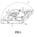
- Fig. 1 is a schematic diagram showing an infrared sensor IC.
- reference numeral 1 denotes a printed board (or a lead frame); reference numeral 2, a compound semiconductor sensor; reference numeral 3, an integrated circuit; and reference numeral 4a, a lead electrode, formed on the printed board 1. Electrodes 13 of the compound semiconductor sensor 2 and the integrated circuit 3, and the electrode 13 of the integrated circuit 3 and the lead electrode 4a are connected by wire bonding 4b, respectively.
- Reference numeral 5 denotes a package cover. That is, the compound semiconductor sensor 2 and the integrated circuit 3 are provided (arranged) on the printed board 1 using hybrid formation.
- the “compound semiconductor sensor” is means for detecting an incident infrared radiation, and for outputting the detection results as an electric signal, i.e., an infrared sensor.
- the “integrated circuit” is a circuit wherein a plurality of circuit elements are formed on a substrate or in a substrate, and means for processing an infrared detection signal (electric signal) output by the compound semiconductor sensor to perform predetermined operation.
- hybrid formation formed in the hybrid manner
- an arbitrary substrate can be used to form the compound semiconductor sensor of the infrared sensor IC for this mode of the invention.
- a monocrystal substrate such as a GaAs substrate or an Si substrate, is preferably used. Further, the monocrystal substrate may be an n-type doped or a p-type doped using donor impurities or acceptor impurities.
- the compound semiconductor sensor may be adhered to another substrate using an adhesive, and the insulating substrate may be peeled off.
- the compound semiconductor layer included in the compound semiconductor sensor is formed using various film deposition methods.
- the molecular beam epitaxy (MBE) or the metal organic vapor phase epitaxy (MOVPE) is an appropriate method. Using this growth method, a desired compound semiconductor layer can be deposited.
- an arbitrary material can be used for the first compound semiconductor layer so long as indium (In) and antimony (Sb) are contained in the semiconductor layer, and above all, InSb, InAsSb, InSbBi, InAsSbBi, InTlSb, InTlAsSb, InSbN, InAsSbN, etc., are preferable.
- x in the As composition ratio is 0, i.e., when there is a wavelength of about 7.3 ⁇ m or shorter at room temperature, the sensitivity for InSb is obtained.
- Eg ⁇ 0.12 eV is established, and the compound semiconductor layer becomes more appropriate for infrared detection, with the peak wavelength being in the 10- ⁇ m band.
- a more preferable range for x is 0.2 ⁇ x ⁇ 0.5.
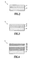
- Fig. 2 is a cross-sectional view of an example for a first compound semiconductor layer 7 formed on a GaAs substrate 6.
- the compound semiconductor layer may build a heterojunction formed of a second compound semiconductor layer and a third compound semiconductor layer.
- An arbitrary material can be used for the second compound semiconductor layer for the mode of the invention, so long as indium (In) and antimony (Sb) are contained in the semiconductor layer.
- an arbitrary material that contains antimony and differs from that for the second compound semiconductor layer may be used.
- a preferable combination of the third compound semiconductor layer/the second compound semiconductor layer is, for example, GaSb/InSb, GaInSb/InSb, InSb/InAsSb, GaSb/InAsSb or GaInSb/InAsSb.
- a preferable range for x in the InAs x Sb 1-x mixed crystal is 0.1 ⁇ x ⁇ 0.6, and a more preferable range for x is 0.2 ⁇ x ⁇ 0.5.
- Fig. 3 is a cross-sectional view of an example compound semiconductor sensor 2 that includes a second compound semiconductor layer 8/a third compound semiconductor layer 9, which are formed on the GaAs substrate 6 (electrodes 13 are not shown).
- the symbol / When the symbol / is used in the specification, it means that material written to the left of the symbol / is formed on a material written to the right of the symbol /. Thus, in the above described case of the third compound semiconductor layer/the second semiconductor layer, it means that the third compound semiconductor layer is formed on the second compound semiconductor layer.
- the first compound semiconductor layer, the second semiconductor layer and the third semiconductor layer may also be p-type doped.
- Be, Zn, C, Mg or Cd is used as a preferable p-type dopant.
- the doping density is the density of the impurity atoms doped in a compound semiconductor.
- the p-type doping density is 1 x 10 16 to 1 x 10 17 atoms/cm 3 , and more preferably, 2 x 10 16 to 5 x 10 16 atoms/cm 3 .
- An infrared sensor wherein the first compound semiconductor layer, the second semiconductor layer and the third compound semiconductor layer are used for the compound semiconductor sensor is generally called a photo conductive infrared sensor.
- sensitivity R pc is represented by expression 1.
- ⁇ denotes an infrared wavelength
- h denotes Planck's constant
- c denotes the speed of light
- ⁇ denotes a quantum efficiency
- 1 denotes the length of a sensor element
- w denotes the width of the sensor element
- V b denotes a bias voltage
- ⁇ denotes the lifetime of a carrier
- d denotes the thickness of a compound semiconductor layer
- N denotes the carrier density of a sensor element
- q denotes the electrical charge of an electron
- ⁇ denotes electron mobility
- R in denotes the element resistance of the sensor element.
- the first compound semiconductor layer, the second semiconductor layer and the third semiconductor layer, which constitute the compound semiconductor sensor of the infrared sensor IC for the mode of this invention, are thin film materials that are non-doped and indicate an n-type. Therefore, it is preferable that these compound semiconductor layers are p-type doped in order to reduce the carrier.density. For the film thickness, thinner films are more appropriate. However, since the quantum efficiency becomes greater as the film thickness is increased, an optimal value exists. Further, since the element resistance can be easily affected by electromagnetic noise when it is too large (equal to or exceeding k ⁇ ), an optimal value for this also exists.
- the compound semiconductor layer also form a superlattice structure wherein a fourth compound semiconductor layer and a fifth compound semiconductor layer are alternately stacked.
- the fourth compound semiconductor layer according to the mode of the invention may be a material that at least contains either indium (In) or antimony (Sb), and the fifth compound semiconductor layer may be a material that at least contains either indium (In) or antimony (Sb) and differs from that of the fourth compound semiconductor layer.
- Fig. 4 is a cross-sectional view of an example compound semiconductor sensor 2 having a superlattice structure wherein a fourth compound semiconductor layer 10 and a fifth semiconductor layer 11 are alternately stacked on the GaAs substrate 6 (electrodes 13 are not shown).
- the superlattice structure is a band structure called Type-II. That is, the superlattice structure is a structure wherein the conduction band of a thin film material forming the fifth compound semiconductor layer is located under the valence band of a thin film material forming the fourth compound semiconductor layer, and wherein a band gap is isolated.
- a band structure holes in the valence band and electrons in the conduction band are separated spatially.
- the lifetime of carriers to be recombined is extended, and the efficiency with which infrared energy is extracted as an electrical signal is improved.
- the sensitivity of the infrared sensor it is considered possible for the sensitivity of the infrared sensor to be increased.
- a stacked layers consisting of compound semiconductors i.e., a stacked layers formed by stacking a compound semiconductor layer that contains indium (In) and antimony (Sb) and is n-type doped, and a compound semiconductor layer that contains indium (In) and antimony (Sb) and is p-type doped is used as the compound semiconductor layer.
- a preferable combination for a stacked layers is a p-n junctional stacked layers, for example, of a p-type doped InSb/a p-type doped InAsSb/an n-type doped InSb, a p-type doped GaInSb/a p-type doped InAsSb/an n-type doped GaInSb, or a p-type doped GaInSb/a p-type doped InSb/an n-type doped GaInSb.
- another stacked layers may be considered preferable, including one such as a p-type doped InSb/an n-type doped InSb, a high-density p-type doped InSb/a low-density p-type doped InSb/a n-type doped InSb, or an n-type doped InSb/a low-density p-type doped InSb/a high-density p-type doped InSb.
- Fig. 5 is a cross-sectional view of an example compound semiconductor sensor 2 wherein a stacked layers 12 formed of compound semiconductors is deposited on an n-type GaAs substrate 6 (electrodes 13 are not shown).
- the compound semiconductor stacked layers 12 includes three layers, a high-density n-type doped layer 12a/a low-density p-type doped layer 12b/a high-density p-type doped layer 12c.
- the "stacked layers” is a compound semiconductor film having a stacked layer structure wherein a plurality of semiconductors are stacked.
- the compound semiconductor stacked layers 12 have a three-layer structure having a high-density p-type doped layer/a low-density p-type doped layer/a high-density n-type doped layer.
- the doping density of the high-density p-type doped layer is 6 x 10 17 to 5 x 10 18 atoms/cm 3 , and more preferably 1 x 10 18 to 4 x 10 18 atoms/cm 3 .
- the doping density of the low-density p-type doped layer is 1 x 10 16 to 1 x 10 18 atoms/cm 3 , and more preferably 1 x 10 16 to 1 x 10 17 atoms/cm 3 .
- the doping density of the high-density n-type doped layer is 6 x 10 17 to 5 x 10 18 atoms/cm 3 , and more preferably falls within the range 1 x 10 18 to 4 x 10 18 atoms/cm 3 .
- an infrared sensor using a p-n junctional stacked layers is a photovoltaic infrared sensor, and the sensitivity R pv of the photovoltaic infrared sensor is represented by expression 2.
- R PV q ⁇ hc ⁇ ⁇ ⁇ R in
- the device in order to increase the sensitivity of the infrared sensor, it is preferable that the device have a large resistance and that the device have a substantial film thickness to increase the quantum efficiency. Further, when a reverse bias voltage is applied to the p-n junctional stacked layers, a carrier can be extracted, as an electrical signal, more efficiently. As a result, a higher sensitivity, for an infrared sensor, can be obtained. However, when the element resistance would be easily affected by electromagnetic noise when it is too great (equal to or exceeding k ⁇ ), there is an optimal value. Furthermore, instead of applying the reverse bias voltage, a method for measuring the open circuit voltage of an element in the zero-bias state is also an appropriate measurement method. This method will be described in detail later.
- the buffer layer 14 can be employed for the buffer layer 14 that is generally 100 nm to 1 ⁇ m and is preferably about 150 nm to 600 nm.
- a composition for the buffer layer 14 it is preferable that a composition having a lattice constant that is as near as possible to that of the material for the compound semiconductor layer, grown on the buffer layer 14, is selected.
- the buffer layer 14 may be formed between the GaAs substrate 6 and the first compound semiconductor layer 7. That is, the purpose here is, by forming the buffer layer 14 between the GaAs substrate 6 and the compound semiconductor layer, as described above, to relax the lattice misfit between the GaAs substrate 6 and the compound semiconductor layers formed atop it and to improve the crystallinity, etc., of the compound semiconductor layers. Therefore, a single compound semiconductor layer, a plurality of layers or a lamination having a plurality of layers may be formed on the buffer layer 14.
- the element characteristics of the infrared sensor can also be improved, the sensitivity increased, and the noise reduced.
- the film thickness of this layer is 0.5 ⁇ m to 10 ⁇ m, preferably 0.7 ⁇ m to 5 ⁇ m and more preferably 1 ⁇ m to 4 ⁇ m.
- the total film thickness of the second compound semiconductor layer and the third compound semiconductor layer is 0.5 ⁇ m to 10 ⁇ m, preferably 1 ⁇ m to 5 ⁇ m and more preferably 2 ⁇ m to 4 ⁇ m.
- the film thicknesses of the fourth compound semiconductor layer and the fifth compound semiconductor layer for one period must be small, so as to form a mini-band.
- the film thickness for one period preferably falls within the range 1 nm to 15 nm, more preferably 2 nm to 10 nm and even more preferably 3 nm to 7 nm.
- the process for fabricating the compound semiconductor sensor of the infrared sensor IC first, using mesa etching, element separation is performed for compound semiconductor layers that are formed using the above described growth method. Then, an SiN protective film is deposited on the surfaces of the substrate and the compound semiconductor layers obtained by element separation. Thereafter, the opening of windows for electrodes is performed in the SiN protective film (passivation film), and the electrodes are formed using the lift off method.
- Au/Ti is preferably used as the electrodes 13. In this case, Au/Ti means that electrodes are formed on an underlayer in the order Ti and Au. Then, dicing is performed to obtain a chip for the compound semiconductor sensor.
- the above described process is an example processing sequence the manufacture of the compound semiconductor sensor according to the mode of the invention.
- Fig. 7 is a cross-sectional view of an example compound semiconductor sensor 2 (a photo conductive infrared sensor) that uses a first compound semiconductor layer 7.
- Fig. 8 is a cross-sectional view of an example compound semiconductor sensor 2 (a photovoltaic infrared sensor) that employs a p-n junctional stacked layers 12.
- an amplification circuit, a chopping circuit, etc. are mounted on the Si substrate of the integrated circuit, and the integrated circuit is formed using a normal CMOS line.
- the production method is not limited to this.
- the compound semiconductor sensor 2 and the integrated circuit 3 are connected to the printed board 1, such as a glass epoxy substrate, by die bonding, and the predetermined electrodes 13 are electrically connected, respectively, using the wire bonding 4b.
- the compound semiconductor sensor 2 is mounted on the integrated circuit 3, and the two are connected together, electrically using wire bonding.
- the size of the infrared sensor IC can be reduced even more.
- an arbitrary material can be used so long as the transmittance of an infrared radiation having a wavelength of equal to or longer than 5 ⁇ m is high, and especially when the infrared transmittance near the 10- ⁇ m band is high.
- a resin material such as polyethylene, can also be used as a package cover if film thickness is reduced.
- a sensor and an IC section are arranged within a hollow package formed of a plastic or a ceramic, and that the sensor, the IC section and the electrode of a package are electrically connected using wire bonding or flip-chip bonding, and that the surface of the package is covered with a filter, such as Si.
- a filter such as Si.
- the incident direction of an infrared radiation may be either from the surface of the sensor or from the substrate that constitutes the reverse side.
- a filter that cuts off light around or equal to or shorter than 5 ⁇ m may be provided in order to completely avoid affects produced by light (a near-infrared radiation of 5 ⁇ m or shorter, or visible light) emitted by objects other than human beings. It is also preferable that a Fresnel lens is provided in order to define the distance and the direction for detection and to improve condensing.
- the photon infrared sensor that employs compound semiconductors has superior properties, high speed and high sensitivity.
- a photodiode infrared sensor having a PN junction and a photodiode infrared sensor having a PIN structure, wherein a non-doped layer or a layer doped at a very low density is inserted at a PN junction, are appropriately used for the compound semiconductor sensor of the infrared sensor IC of this invention.
- reducing a leak current at the infrared sensor is important for increasing the sensitivity.
- a diffusion current is the main factor of a leak current.
- a diffusion current is proportional to the square of an intrinsic carrier density ni of a semiconductor that is included in an infrared sensor.
- ni 2 is represented by expression 3.
- n i 2 N c ⁇ N v ⁇ exp - E g kT
- N c and N v denote effective state densities of a conduction band and a valence band, respectively.
- E g denotes an energy band gap.
- N c , N v and E g denote unique values of semiconductor materials.
- the energy band gap in order for an infrared radiation having a wavelength of 5 ⁇ m or longer to be absorbed by a semiconductor, the energy band gap must be very small, about 0.25 [eV] or lower.
- the intrinsic carrier density is increased, i.e., 6 x 10 15 [cm 3 ] or greater, and accordingly, the diffusion current is increased. Therefore, the leak current becomes larger.
- the infrared detection element section it is necessary for the infrared detection element section to be cooled using liquid nitrogen, a refrigeration unit such as a Stirling cooler, electron cooling utilizing the Peltier effect, etc., so that the intrinsic carrier density must be reduced.
- Fig. 10 is a cross-sectional view of a compound semiconductor infrared sensor according to one mode of the invention. The features of the structure and the operation of this sensor will now be described while referring to Fig. 10 .
- a sixth compound semiconductor layer 16 which is an n-type doped layer (also called an n layer), is formed on a substrate 15.
- Electrodes 19 are formed on the eighth compound semiconductor layer 18 and in an area of the sixth compound semiconductor layer 16 wherein the seventh compound semiconductor layer 17 is not formed.
- a passivation film 20 is deposited to protect the surface of the compound semiconductor infrared sensor having this structure. At this time, the passivation film 20 does not cover the electrodes 19.
- the infrared radiation When an infrared radiation enters the infrared sensor in Fig. 10 , the infrared radiation is absorbed at the seventh compound semiconductor layer 17, which is a light absorption layer, and pairs of electrons and positive holes are generated.
- the pairs of generated electrons and positive holes are separated in accordance with a potential difference between the sixth compound semiconductor layer 16, which is an n layer, and the eighth compound semiconductor layer 18, which is a p layer, i.e., in accordance with a built-in potential, and electrons are moved to the n-layer side while the positive holes are moved to the p-layer side and become a photo current.
- the positive holes can not be extracted as a photo current.
- the diffusion of a carrier in the forward direction of the PIN diode is a diffusion current.
- the eighth compound semiconductor layer which is a p layer
- the intrinsic carrier density ni of the p-layer portion can be reduced, as represented by expression 3. Therefore, the diffusion current flowing from the seventh compound semiconductor layer 17 to the eighth compound semiconductor layer 18 can be suppressed.
- Fig. 11 is a diagram showing the energy band of the compound semiconductor infrared sensor explained while referring to Fig. 10 .
- E denotes the energy of an electron
- E F denotes Fermi energy
- E C denotes a conduction band level
- E V denotes a valence band level.
- arrows in the drawing indicate directions of movement of an electron generated by the incidence of the infrared radiation; a direction of movement (an arrow A) of an electron serving as a photo current; and a direction of movement (an arrow B) of an electron serving as a diffusion current. That is, as is apparent from the energy band diagram in Fig.
- the eighth compound semiconductor layer 18 serves as a barrier layer for the diffusion of electrons to the p layer side.
- the flow of positive holes generated by the incidence of the infrared radiation is not interrupted.
- the leak current can be greatly reduced.
- electrons generated by the incidence of the infrared radiation flow easily in the direction A of a photo current, a photo current to be extracted can be increased. That is, the external quantum efficiency of the sensor is improved. As a result, the sensitivity of the element can be increased remarkably.
- the lamination order of the individual compound semiconductor layers is very important for one mode of the invention.
- An explanation will be given for the reason that, first, the sixth compound semiconductor layer, which is n-type doped, is grown on the substrate, the seventh compound semiconductor layer., which is p-type doped, is grown on the sixth compound semiconductor layer, and further, the eighth compound semiconductor layer, which is p-type doped at a higher density than the seventh compound semiconductor layer and has a larger band gap than the second compound semiconductor layer, is grown on the seventh compound semiconductor layer.
- the sixth compound semiconductor layer 16 is a buffer layer, provided so that, with appropriate crystallinity, the seventh compound semiconductor layer 17, which is a light absorption layer, can be grown on the substrate.
- the sixth compound semiconductor layer 16 serves as a contact layer fitted with electrodes.
- the sheet resistance is the main factor in the resistance of the sensor.
- the resistance R of the sensor causes Johnson noise, which is heat noise, i.e., as the resistance of the sensor becomes higher, the noise is increased.
- the sixth compound semiconductor layer 16 is a layer having a small sheet resistance.
- the sheet resistance can be better reduced by n-type doping than by p-type doping.
- n-type doping is preferable for the sixth compound semiconductor layer 16.
- the eighth compound semiconductor layer 18 when the eighth compound semiconductor layer 18 is grown as a barrier layer, and then the seventh compound semiconductor layer 17 is grown as a light absorption layer, effects suppressing the diffusion current are the same as those obtained for the lamination structure shown in Fig. 10 . Thus, this is preferable as the structure of the compound semiconductor infrared sensor.
- the seventh compound semiconductor layer 17 is formed, with hetero growth including lattice misfit, on the eighth compound semiconductor layer 18 for which the lattice constant of a crystal differs. Therefore, crystal defects tend to occur in the seventh compound semiconductor layer 17, which is a light absorption layer, and annihilation of pairs of electrons and positive holes generated by infrared absorption can easily occur. That is, the quantum efficiency of the sensor tends to be reduced. Therefore, it is preferable that the growth of the eighth compound semiconductor layer 18, which is a barrier layer, follow the growth of the seventh compound semiconductor layer 17, which is a light absorption layer.
- the sixth compound semiconductor layer 16, which is n-type doped is grown on the substrate 15. Thereafter, the seventh compound semiconductor layer 17, which is p-type doped, is grown in a predetermined area on the sixth compound semiconductor layer 16. Further, the eighth compound semiconductor layer 18, which is p-type doped at a higher density than the seventh compound semiconductor layer 17 and which has a larger band gap than the seventh compound semiconductor layer 17, is grown on the seventh compound semiconductor layer 17. According to the mode of the invention, it is preferable that the compound semiconductor infrared sensor is provided by the growth method that employs this order.
- a ninth compound semiconductor layer which is p-type doped at a density equal to or higher than the eighth compound semiconductor layer 18, may be further grown on the eighth compound semiconductor layer 18. This will be explained later.
- the eighth compound semiconductor layer 18 should be a material having a smaller lattice constant.
- the difference with the lattice constant of the seventh compound semiconductor layer 17, which has a small band gap tends to be increased, and crystal defects due to hetero growth tend to occur in the eighth compound semiconductor layer 18, which is a barrier layer. This crystal defect causes a leak current due to the defect.
- the size of the band gap is determined by the effects both for suppressing a diffusion current and for improving the crystallinity of the eighth compound semiconductor layer 18.
- a jump also called a spike
- Fig. 11 appears in the valence band because of a difference between the energy band structures of the materials.
- the tip of the spike projects outward from the valence band of the seventh compound semiconductor layer, the flow of positive holes generated by infrared absorption is interrupted. In order to prevent this, p-type doping must be appropriately performed for the eighth compound semiconductor layer 18.
- an arbitrary material can be used for the sixth compound semiconductor layer 16 so long as indium (In) and antimony (Sb) are contained in the semiconductor layer, and InSb is used as a preferable material. Since of the compound semiconductors InSb has high electron mobility, the sheet resistance can be lowered. Further, an arbitrary material can be used for the seventh compound semiconductor layer 17 so long as indium (In) and antimony (Sb) are contained in the semiconductor layer, and InSb, InAsSb, InSbN, etc., are used as preferable materials.
- the x of the As composition ratio is 0, i.e., when the wavelength is about 7. 3 ⁇ m or shorter at room temperature, the sensitivity of InSb is obtained.
- E g ⁇ 0.12 eV is established, and InSb is a compound semiconductor layer that is more appropriate for infrared detection, having a peak wavelength that is in a 10- ⁇ m band.
- a more preferable range for x is 0.2 ⁇ x ⁇ 0.5.
- the band gap of an InSb 1-y N y mixed crystal (0 ⁇ y ⁇ 0.01) includes a larger non-linear factor, and that the band gap approaches 0 when the composition y of nitrogen N is only 0.01. Therefore, by employing a system that uses InSb 1-y N y , which is similar to the lattice fit of InSb (sixth compound semiconductor layer), an infrared radiation having a longer wavelength than that absorbed by InSb can be absorbed.
- a growth method for gradually changing the composition from 0 to x or 0 to y is preferably employed in order to suppress the occurrence of crystal defects due to hetero growth.
- a material for which the band gap is larger than that of the seventh compound semiconductor layer 17 can be used for the eighth compound semiconductor layer 18.
- One of AlInSb, GaInSb, AlAs, GaAs, InAs, AlSb, GaSb, AlAsSb, GaAsSb, AlGaSb, AlGaAs, AlInAs, GaInAs, AlGaAsSb, AlInAsSb, GaInAsSb, AlGaInSb, AlGaInSb and AlGaInAsSb is preferable as the eighth compound semiconductor layer 18.
- a preferable range for z is 0.01 ⁇ z ⁇ 0.7, and more preferably, 0.1 ⁇ z ⁇ 0.5.
- the film thickness of the sixth compound semiconductor layer 16 is as great as possible in order to reduce sheet resistance. It should be noted, however, that, when the film thickness of the sixth compound semiconductor layer 16 is increased, an enormous time is required for the growth of a film, and mesa etching, etc., for device separation would be difficult.
- the film thickness of the sixth compound semiconductor layer 16 is preferably equal to or greater than 0.3 ⁇ m to equal to or smaller than 2 ⁇ m, and more preferably equal to or greater than 0.5 ⁇ m to equal to or smaller than 1 ⁇ m.
- the film thickness of the seventh compound semiconductor layer 17 is as great as possible in order to increase infrared absorption. It should be noted, however, that when the film thickness of the seventh compound semiconductor layer 17 is increased, as well as for the sixth compound semiconductor layer 16, an enormous time is required for the growth of a film, and etching, etc., for device separation is difficult.
- the film thickness of the seventh compound semiconductor layer 17 is preferably equal to or greater than 0.5 ⁇ m to 3 ⁇ m, and more preferably, is equal to or greater than 1 ⁇ m to equal to or smaller than 2 ⁇ m.
- the film thickness of the eighth compound semiconductor layer 18 is as small as possible in order to reduce device resistance. It should be noted, however, that a film thickness is required that is sufficient for the prevention of the occurrence of a tunnel leak between the electrode 19 and the seventh compound semiconductor layer 17.
- the film thickness of the eighth compound semiconductor layer 18 is preferably equal to or greater than 0.01 ⁇ m, and more preferably, is equal to or greater than 0.02 ⁇ m. Assuming that a rectangular potential barrier is provided, the tunnel probability P of electrons is represented by expression 5 and expression 6.
- the tunnel probability P is about 0.002, which is satisfactorily small.
- the n-type doping density for the sixth compound semiconductor layer 16 is as high as possible, and is equal to or higher than 1 x 10 18 atoms/cm 3 .
- the seventh compound semiconductor layer 17 may be either an intrinsic semiconductor that is not doped, or may be p-type doped.
- the p-type doping density of the seventh compound semiconductor layer 17 is adjusted, so that a sufficiently large band offset can be obtained relative to conduction bands of the sixth compound semiconductor layer 16 and the eighth compound semiconductor layer 18.
- the p-type doping density for the seventh compound semiconductor layer 17 is equal to or higher than 1 x 10 16 atoms/cm 3 to lower than 1.0 x 10 18 atoms/cm 3 .
- the p-type doping density for the eighth compound semiconductor layer 18 is equal to or higher than 1 x 10 18 atoms/cm 3 , so that the spike in the valance band, at the junction interface between the seventh compound semiconductor layer 17 and the eighth compound semiconductor layer 18, does not interrupt the flow of positive holes that are generated by infrared absorption.
- Si, Te, Sn, S, Se, Ge, etc. can be used as an n-type dopant. Since, above all, Sn has a higher activation ratio relative to InSb, and can reduce sheet resistance, Sn is more preferably used. Further, Be, Zn, Cd, C, Mg, etc., can be used as a p-type dopants. Since above all, Zn has a higher activation ratio relative to InSb and is less poisonous, Zn is more preferably used.
- FIG. 12 is a cross-sectional structure of this device structure. The characteristic of the structure of the compound semiconductor infrared sensor will now be described while referring to Fig. 12 .
- the eighth compound semiconductor layer 18 that serves as a barrier layer is a material having a large band gap, and generally, the carrier mobility is small. Thus, the contact resistance relative to the electrode 19 is increased, and causes the previously described Johnson noise.
- a ninth compound semiconductor layer 21 is formed on the eighth compound semiconductor layer 18 by using a material having a lower electrical resistance than the eighth compound semiconductor layer 18, the increase in the resistance can be suppressed. Further, in order to reduce the electrical resistance, it is preferable that appropriate p-type doping is performed for the ninth compound semiconductor layer 21.
- This ninth compound semiconductor layer 21 An arbitrary material can be used for this ninth compound semiconductor layer 21 so long as indium (In) and antimony (Sb) are contained in the semiconductor layer, and InSb, for which the carrier mobility is high, is a preferable material.
- the ninth compound semiconductor layer 21 must only have a film thickness great enough to reduce contact resistance, and 0.1 ⁇ m or greater to 2 ⁇ m or smaller is preferable.
- Be, Zn, Cd, C, Mg, etc. are preferably used as p-type dopants for the ninth compound semiconductor layer 21.
- Zn is preferable because the activation ratio relative to InSb is higher and the toxicity is low.
- the p-type doping density is preferably equal to or higher than 1 x 10 18 atoms/cm 3 in order to obtain a small resistance at the film.
- Fig. 13 is a cross-sectional view of one part of a compound semiconductor sensor wherein a plurality of unit devices are connected in series in the above described manner.
- Fig. 14 is a top view of the structure shown in Fig. 13 .
- compound semiconductor infrared sensors which are unit devices obtained by device separation, are contiguously connected in series by electrodes 19 on the substrate 15. Let us focus on a specific compound semiconductor infrared sensor of those contiguously connected in series on the substrate 15.
- the sixth compound semiconductor layer 16 of the specific sensor and the ninth compound semiconductor layer 21, which is located in a sensor adjacent to the specific sensor, are electrically connected in series by the electrode 19.
- the ninth compound semiconductor layer 21 of the specific sensor and a sixth compound semiconductor layer 16 of a sensor located in a sensor adjacent to the specific sensor are electrically connected in series by the electrode 19.
- compound semiconductor infrared sensors located at both ends of a series connection are respectively connected to electrode pads 22.
- a broken line in Fig. 14 indicates that the individual sensors are contiguously and repetitively connected in accordance with the arrangement. Further, in Fig. 14 , for the sake of convenience, a passivation film 20 is not shown, to make it easy to understand the structure of electrode connection between devices.
- the substrate 15 must be a substrate that is semi-insulating, or one for which the thin compound semiconductor film portion and the substrate portion can be insulating, that permits the growth of a singlecrystal for a thin compound semiconductor film.
- a material that transmits an infrared radiation is used for such a substrate, infrared light can enter from the reverse face of the substrate. This case is more preferable, because the blocking of infrared light by the electrode does not occur, and the light-detecting area of the device can be more extensive.
- a preferable material for the substrate is semi-insulating Si or GaAs, etc.
- the individual compound semiconductor layers included in the infrared sensor according to the mode of the invention are formed by using various film deposition methods.
- the molecular beam epitaxy (MBE) method and the metal organic vapor phase epitaxy (MOVPE) method are preferable methods. Therefore, using these methods, the individual compound semiconductor layers can be grown as requested.
- the processing methods for devices are not especially limited. For example, for the compound semiconductor layers deposited using the above growth methods, a step is formed using acid or ion milling to obtain a contact with the sixth compound semiconductor layer 16. Then, for the compound semiconductor layers for which a step has been formed, mesa etching is performed for device separation.
- the surfaces of the substrate 15 and the compound semiconductor layers obtained by device separation are covered with the passivation film 20 formed, for example, of SiN or SiO 2 , with only the electrode 19 portions opened as windows, and electrodes of Au/Ti, Au/Cr, etc., are formed using the lift off method. In this manner, the chip for the compound semiconductor sensor is prepared.
- the passivation film 20 formed, for example, of SiN or SiO 2 , with only the electrode 19 portions opened as windows, and electrodes of Au/Ti, Au/Cr, etc., are formed using the lift off method.
- a method for applying a reverse bias to electrodes and fetching a signal as a current is a preferable measurement method for sensing an infrared radiation by using the infrared sensor, shown in Fig. 10 or 12 described above, made of the unit device shown in Fig. 10 or 12 , and the infrared sensor shown in Figs. 13 and 14 , wherein a plurality of unit devices are connected in series.
- the present inventors adopted a photovoltaic measurement method to set a zero bias for electrodes, and to read a signal as an open circuit voltage.
- the photovoltaic measurement method since a current does not flow through devices, only Johnson noise occurs. Therefore, the infrared sensor can be used at a low frequency. Further, according to this method, since heat generation by a device due to Joule heat does not occur, the measurement error can be extremely small.
- a signal obtained by a conventional photovoltaic measurement method is weak, an appropriately strong signal can be obtained by using the compound semiconductor infrared sensor according to the seventh mode of the invention.
- the compound semiconductor infrared sensor for the seventh mode of the invention is arranged, in the hybrid manner, in a single package with an integrated circuit that processes an electrical signal output by the sensor, an epoch-making, microminiature compound semiconductor infrared sensor IC, which is robust relative to noise and temperature fluctuation and is more sensitive at room temperature, can be obtained.
- non-doped InAs 0.23 Sb 0.77 of 2 ⁇ m was grown on a GaAs substrate.
- the film characteristics of a thin InAsSb film were measured using the van der Pauw method, and an electron mobility of 35,000 cm 2 /Vs at room temperature, a sheet resistance (device resistance) of 20 ⁇ , and a carrier density of 1 x 10 17 atoms/cm 3 were obtained.
- a compound semiconductor sensor was then fabricated by using this thin compound semiconductor film. First, for device separation, mesa etching was performed for the compound semiconductor film deposited on the GaAs substrate, and then, the entire surface (the GaAs substrate and the compound semiconductor film deposited on the substrate) was covered with an SiN protective film.
- a cross section of a compound semiconductor sensor for a first embodiment is as shown in Fig. 7 .
- An integrated circuit on which an amplification circuit, a chopping circuit, etc., were mounted was fabricated using a common CMOS process. Thereafter, the compound semiconductor sensor and the integrated circuit were mounted on the same substrate using die bonding, and were electrically connected using wire bonding. A package cover was attached to complete an infrared sensor IC for the first embodiment.
- D * denotes an indicator for a detectivity, and is represented as a value obtained by multiplying the reciprocal of an incident light intensity (W/Hz 1/2 ) required to obtain an S/N ratio of 1 by the 1/2 power of the light receiving area of a detection device. It was thereafter confirmed that a characteristic of the infrared sensor IC, according to the first embodiment, is that, in spite of being a simple package, it is not easily affected by electromagnetic noise and thermal fluctuation.
- non-doped InSb of 1 ⁇ m and non-doped InAs 0.23 Sb 0.77 of 2 ⁇ m were grown on a GaAs substrate in the named order.
- the film characteristics of a thin compound semiconductor layer were measured using the van der Pauw method, and an electron mobility of 51, 000 cm 2 /Vs at room temperature, a sheet resistance (device resistance) of 20 ⁇ , and a carrier density of 9 x 10 16 atoms/cm 3 were obtained.
- a compound semiconductor sensor was then fabricated by using this thin compound semiconductor film.
- mesa etching was performed for the compound semiconductor film deposited on the GaAs substrate, and then, the entire surface (the GaAs substrate and the compound semiconductor film deposited on the substrate) was covered with an SiN protective film. Following this, only the electrode portions on the deposited SiN protective film were opened as windows, Au/Ti was deposited using EB evaporation, and electrodes were formed using the lift off method.
- the light-receiving areas were designed to be 35 ⁇ m x 115 ⁇ m.
- An integrated circuit on which an amplification circuit, a chopping circuit, etc., were mounted was fabricated using a common CMOS line. Thereafter, the compound semiconductor sensor and the integrated circuit were mounted on the same substrate using die bonding, and were electrically connected using wire bonding. A package cover was attached to complete an infrared sensor IC for a second embodiment.
- mesa etching was performed for the compound semiconductor film deposited on the GaAs substrate, and then, the entire surface (the GaAs substrate and the compound semiconductor film deposited on the substrate) was covered with an SiN protective film. Following this, only the electrode portions on the deposited SiN protective film were opened as windows, Au/Ti was deposited using EB evaporation, and electrodes were formed using the lift off method.
- the light-receiving areas were designed to be 35 ⁇ m x 115 ⁇ m.
- An integrated circuit on which an amplification circuit, a chopping circuit, etc., were mounted was fabricated using a common CMOS line. Thereafter, as shown in Fig. 9 , the integrated circuit was mounted on the substrate using die bonding, the compound semiconductor sensor was mounted on the same substrate using die bonding, and they were electrically connected using wire bonding. A package cover was attached to complete an infrared sensor IC for the third embodiment.
- a compound semiconductor sensor was fabricated by using this thin compound semiconductor film.
- mesa etching was performed for the compound semiconductor film deposited on the n-type GaAs substrate, and then, the entire surface (the n-type GaAs substrate and the compound semiconductor film deposited on the substrate) was covered with an SiN passivation film. Following this, only the electrode portions on the deposited SiN passivation film were opened as windows, Au/Ti was deposited using EB evaporation, and electrodes were formed using the lift off method. The light-receiving areas were designed to be 35 ⁇ m x 115 ⁇ m.
- a cross section of a compound semiconductor sensor for a fourth embodiment is as shown in Fig. 8 .
- An integrated circuit on which an amplification circuit, a chopping circuit, etc., were mounted was fabricated using a common CMOS line. Thereafter, the compound semiconductor sensor and the integrated circuit were mounted on the same substrate using die bonding, and were electrically connected using wire bonding. A package cover was attached to complete an infrared sensor IC for the fourth embodiment.
- Al 0.05 Ga 0.5 Sb of 150 nm was grown as a buffer layer on a GaAs substrate, and then non-doped InSb of 0.5 ⁇ m and InAs 0.23 Sb 0.77 of 2 ⁇ m were grown.
- the film characteristics of a thin InAsSb film were measured using the van der Pauw method, and an electron mobility of 45,000 cm 2 /Vs at room temperature, a sheet resistance (device resistance) of 40 ⁇ , and a carrier density of 5 x 10 16 atoms/cm 3 were obtained.
- a compound semiconductor sensor was then fabricated by using this thin compound semiconductor film.
- mesa etching was performed for the compound semiconductor film deposited on the GaAs substrate, and then, the entire surface (the GaAs substrate and the compound semiconductor film deposited on the substrate) was covered with an SiN protective film. Following this, only the electrode portions on the deposited SiN protective film were opened as windows, Au/Ti was deposited using EB evaporation, and electrodes were formed using the lift off method.
- the light-receiving areas were designed to be 35 ⁇ m x 115 ⁇ m.
- An integrated circuit on which an amplification circuit, a chopping circuit, etc., were mounted was fabricated using a common CMOS line. Thereafter, the compound semiconductor sensor and the integrated circuit were mounted on the same substrate using die bonding, and were electrically connected using wire bonding. A package cover was attached to complete an infrared sensor IC for a fifth embodiment.
- non-doped InSb of 1 ⁇ m and p-type doped InAs 0.23 Sb 0.77 of 2 ⁇ m were grown on a GaAs substrate in the named order.
- the film characteristics of a thin InAsSb film was measured using the van der Pauw method, and an electron mobility of 41,000 cm 2 /Vs at room temperature, a sheet resistance (device resistance) of 150 ⁇ and a carrier density of 1.5 x 10 16 atoms/cm 3 were obtained.
- the purpose of p-type doping in the sixth embodiment is to provide compensation for the carriers of electrons in the InAsSb layer and the reduction in the carrier density.
- the electron mobility was lowered; however, the carrier density of electrons could be reduced by p-type doping, and the sheet resistance was increased. Further, the same effects can be obtained by p-type doping of the non-doped InSb layer.
- a compound semiconductor sensor was fabricated in the same manner as in the second embodiment.
- An integrated circuit was also manufactured in the same manner as in the second embodiment, and an infrared sensor IC for the sixth embodiment was completed.
- a compound semiconductor infrared sensor was then prepared using the thin compound semiconductor film. First, for the thin compound semiconductor film, a step was formed using acid or ion milling to obtain a contact with the p-type doped InSb layers. Then, mesa etching, for device separation, was performed for the thin compound semiconductor film for which the step was formed.
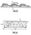
- FIG. 15 A cross section of a compound semiconductor infrared sensor according to a seventh embodiment is shown in Fig. 15 .
- the compound semiconductor infrared sensor for the seventh embodiment has the structure of a so-called PN junctional diode.
- reference numeral 23 denotes a semi-insulating GaAs monocrystal substrate; reference numeral 24, a p-type doped InSb layer; reference numeral 25, an n-type doped InSb layer; reference numeral 26, an SiN passivation film; and reference numeral 27, an Au/Ti electrode.
- the compound semiconductor infrared sensor was irradiated using an infrared radiation, and the open circuit voltage of the device was measured as an output voltage. It should be noted that the sensor temperature during the measurement was room temperature (27°C). An incident infrared radiation was emitted by using a blackbody furnace at 500 K, which was located at a distance of 10 cm from the sensor. With this arrangement, an infrared radiation was emitted, directed toward the substrate side of the sensor. The energy of the incident infrared radiation was 1.2 mW/cm 2 . The frequency for light chopping was 10 Hz, and Si was used as a filter for cutting light, such as visible light.
- a compound semiconductor infrared sensor was then prepared using the thin compound semiconductor film.
- a step was formed using acid or ion milling to obtain a contact with the InSb layers that were p-type doped at high densities. Then, mesa etching, for device separation, was performed for the thin compound semiconductor film for which the step was formed. Thereafter, the entire surface (the GaAs substrate and the compound semiconductor film deposited on the substrate) was covered with an SiN passivation film. Following this, only the electrode portions of the SiN protective film were opened as windows, Au/Ti was deposited using EB evaporation, and electrodes were formed using the lift off method.
- the light-receiving area was designed to be 225 ⁇ m x 150 ⁇ m.
- FIG. 16 A cross section of a compound semiconductor infrared sensor according to an eighth embodiment is shown in Fig. 16 .
- the compound semiconductor infrared sensor for the eighth embodiment has the structure of a so-called PIN junctional diode.
- reference numeral 28 denotes an InSb layer that is p-type doped at a high density
- reference numeral 30, an n-type doped InSb layer an InSb layer that is p-type doped at a low density.
- the compound semiconductor infrared sensor was irradiated using an infrared radiation, and the open circuit voltage of the device was measured as an output voltage. It should be noted that the sensor temperature during the measurement was room temperature (27°C). An incident infrared radiation was emitted by using a blackbody furnace at 500 K, which was located at a distance of 10 cm from the sensor. With this arrangement, an infrared radiation was emitted, directed toward the substrate side of the sensor. The energy of the incident infrared radiation was 1.2 mW/cm 2 . The frequency for light chopping was 10 Hz, and Si was used as a filter for cutting light, such as visible light.
- a compound semiconductor infrared sensor was then prepared using the thin compound semiconductor film.
- a step was formed using acid or ion milling to obtain a contact with the InSb layers that were n-type doped at high densities. Then, mesa etching, for device separation, was performed for the thin compound semiconductor film for which the step was formed. Thereafter, the entire surface (the GaAs substrate and the compound semiconductor film deposited on the substrate) was covered with an SiN passivation film. Following this, only the electrode portions of the SiN protective film were opened as windows, Au/Ti was deposited using EB evaporation, and electrodes were formed using the lift off method.
- the light-receiving area was designed to be 225 ⁇ m x 150 ⁇ m.
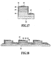
- FIG. 17 A cross section of a compound semiconductor infrared sensor according to a ninth embodiment is shown in Fig. 17 .
- the compound semiconductor infrared sensor for the ninth embodiment has the structure wherein the p-type doped layer 28 and the n-type doped layer 30 are exchanged in the structure of the eighth embodiment.
- the compound semiconductor infrared sensor was irradiated using an infrared radiation, and the open circuit voltage of the device was measured as an output voltage. It should be noted that the sensor temperature during the measurement was room temperature (27°C). An incident infrared radiation was emitted by using a blackbody furnace at 500 K, which was located at a distance of 10 cm from the sensor. With this arrangement, an infrared radiation was emitted, directed toward the substrate side of the sensor. The energy of the incident infrared radiation was 1.2 mW/cm 2 . The frequency for light chopping was 10 Hz, and Si was used as a filter for cutting light, such as visible light.
- the measurement results for the output voltage are also shown in Fig. 22 .
- the output voltage was 155 nV, and it was confirmed that the output voltage was increased more than in the eighth embodiment.
- Sn is used as an n-type dopant. That is, since relative to InSb, Sn has a higher activation ratio than Si, n-type doping at a higher density is enabled, and a greater PN junctional built-in potential is obtained.
- the output voltage V out is a voltage required for the supply of a diffusion current across the potential barrier of a built-in potential V d . Thus, since the built-in potential is great, accordingly, the output voltage is increased. Therefore, the effect of the increase in output could be confirmed when Sn was used as the n-type dopant in the ninth embodiment.
- a compound semiconductor sensor wherein a plurality of devices are connected in series was formed by using a thin compound semiconductor film having the same structure as in the eighth embodiment.
- a step was formed using acid or ion milling to obtain a contact with an InSb layer that was p-type doped at a high density.
- mesa etching was performed for device separation. Thereafter, the entire surface (the GaAs substrate and the compound semiconductor film formed on the substrate) was covered with an SiN passivation film.
- Electrodes were formed so that the InSb layer of a specific device, whereat Zn was doped using 3.5 x 10 18 atoms/cm 3 , was electrically connected to the InSb layer of a device adjacent to the specific device and located on the side whereat the step was formed, whereat Si was doped using 1.8 x 10 18 atoms/cm 3 .
- the light-receiving area of a prepared unit device was 18 ⁇ m x 18 ⁇ m, and a series connection of 125 unit devices was formed on the GaAs substrate. A cross section of a part of the thus obtained sensor is shown in Fig. 18 .
- the compound semiconductor infrared sensor was irradiated using an infrared radiation, and the open circuit voltage of the device was measured as an output voltage. It should be noted that the sensor temperature during the measurement was room temperature (27°C). An incident infrared radiation was emitted by using a blackbody furnace at 500 K, which was located at a distance of 10 cm from the sensor. With this arrangement, an infrared radiation was emitted, directed toward the substrate side of the sensor. The energy of the incident infrared radiation was 1.2 mW/cm 2 . The frequency for light chopping was 10 Hz, and Si was used as a filter for cutting light, such as visible light.
- an output voltage of 12.5 ⁇ V was obtained. That is, it was confirmed that by using the compound semiconductor film structure and the measurement method for measuring an open circuit voltage according to the present invention, the output could be increased by increasing the number of connected devices. This is an extremely large advantage for a quantum infrared sensor when operated at room temperature, for which a signal obtained from a unit device is weak.
- the 125 connected sensors were connected to a signal amplifier, and using a fast Farrier transform (FET) analyzer, generated noise was measured in a darkroom at room temperature (27°C).
- FET Farrier transform
- the noise generated by the signal amplifier was removed and the only noise was that produced by the sensor, it was confirmed that 1/f noise was not found, even at a frequency of 10 Hz or lower.
- the resistance of the infrared sensor was measured using a tester, a value of 12.75 k ⁇ was obtained. And when this value was substituted into expression 4 to calculate the Johnson noise, it was found that the result matched the sensor noise that had been measured.
- the noise of the sensor is only the Johnson noise as determined by the resistance, and a sensor generates only an extremely small amount of noise, in a low frequency area of 10 Hz or less.
- a compound semiconductor sensor wherein a plurality of devices are connected in series was formed by using a thin compound semiconductor film having the same structure as in the ninth embodiment, and using the same mask set as used in the tenth embodiment.
- a step was formed using acid or ion milling to obtain a contact with an InSb layer that was n-type doped at a high density.
- mesa etching was performed for device separation. Thereafter, the entire surface (the GaAs substrate and the compound semiconductor film formed on the substrate) was covered with an SiN passivation film.
- Electrodes were formed so that the InSb layer of a specific device, whereat Sn was doped using 1.0 x 10 19 atoms/cm 3 , was electrically connected to the InSb layer of a device adjacent to the specific device and located on the side whereat the step was formed, whereat Zn was doped using 7.0 x 10 18 atoms/cm 3 .
- the light-receiving area of a prepared unit device was 18 ⁇ m x 18 ⁇ m, and a series connection of 125 unit devices was formed on the GaAs substrate. A cross section of a part of the thus obtained sensor is shown in Fig. 19 .
- the compound semiconductor infrared sensor was irradiated using an infrared radiation, and the open circuit voltage of the device was measured as an output voltage. The obtained result was 22.5 ⁇ V, and compared with the output voltage obtained by using the same number of connected devices in the tenth embodiment, about 1.8 times of output was obtained.
- the sensor temperature during the measurement was room temperature (27°C).
- An incident infrared radiation was emitted by using a blackbody furnace at 500 K, which was located at a distance of 10 cm from the sensor. With this arrangement, an infrared radiation was emitted, directed toward the substrate side of the sensor. The energy of the incident infrared radiation was 1.2 mW/cm 2 .
- the frequency for light chopping was 10 Hz
- Si was used as a filter for cutting light, such as visible light.
- the device resistance of the compound semiconductor infrared sensor was measured using a tester, 9.6 k ⁇ was obtained. That is, it was confirmed that the resistance was lower than the resistance in the tenth embodiment, obtained using the same number of connected units. This is because the n-type doped layer, which had low resistivity, was at the lowermost location to reduce the resistance in the device. It was thus confirmed that, as a result, the noise of the sensor could be reduced to about 0.87 times the noise of the sensor in the tenth embodiment.
- a compound semiconductor infrared sensor was then prepared using the thin compound semiconductor film.
- a step was formed using acid or ion milling to obtain a contact with the p-type doped InSb layers.
- mesa etching for device separation, was performed for the thin compound semiconductor film for which the step was formed.
- the entire surface (the GaAs substrate and the compound semiconductor film deposited on the substrate) was covered with an SiN passivation film.
- only the electrode portions of the SiN protective film were opened as windows, Au/Ti was deposited using EB evaporation, and electrodes were formed using the lift off method.
- the light-receiving area was designed to be 225 ⁇ m x 150 ⁇ m.
- FIG. 20 A cross section of a compound semiconductor infrared sensor according to a twelfth embodiment is shown in Fig. 20 .
- reference numeral 31 denotes an Al 0.2 In 0.8 Sb layer that is p-type doped at a high density.
- the compound semiconductor infrared sensor was irradiated using an infrared radiation, and the open circuit voltage of the device was measured as an output voltage. It should be noted that the sensor temperature during the measurement was room temperature (27°C). An incident infrared radiation was emitted by using a blackbody furnace at 500 K, which was located at a distance of 10 cm from the sensor. With this arrangement, an infrared radiation was emitted, directed toward the substrate side of the sensor. The energy of the incident infrared radiation was 1.2 mW/cm 2 . The frequency for light chopping was 10 Hz, and Si was used as a filter for cutting light, such as visible light.
- the output voltage obtained using the above described arrangement was 242 nV.
- the measurement results are shown in Fig. 22 , as well as in the other embodiments. It was confirmed that, when compared with the ninth embodiment for the PIN diode structure, the output was about 1.6 times as large.
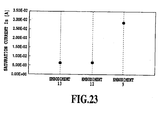
- the saturation current I s represents the magnitude of the diffusion current of the device.
- Fig. 23 The results I s obtained for the twelfth embodiment and the ninth embodiment are shown in Fig. 23 . As shown in Fig. 23 , it could be confirmed that, compared with a device having a PIN diode structure that does not employ an AlInSb barrier layer, the saturation current I s for an infrared sensor wherein an AlInSb barrier layer was formed was reduced by one digit.
- the characteristic that a diffusion current is suppressed by the AlInSb barrier layer could be confirmed. Through the application of this effect, the output was increased.
- a compound semiconductor infrared sensor was then prepared using the thin compound semiconductor film.
- a step was formed using acid or ion milling to obtain a contact with the n-type doped InSb layers.
- mesa etching for device separation, was performed for the thin compound semiconductor film for which the step was formed.
- the entire surface (the GaAs substrate and the compound semiconductor film deposited on the substrate) was covered with an SiN passivation film.
- only the electrode portions of the SiN protective film were opened as windows, Au/Ti was deposited using EB evaporation, and electrodes were formed using the lift off method.
- the light-receiving area was designed to be 225 ⁇ m x 150 ⁇ m.
- a cross section of a compound semiconductor infrared sensor according to a thirteenth embodiment is shown in Fig. 21 .
- the compound semiconductor infrared sensor was irradiated using an infrared radiation, and the open circuit voltage of the device was measured as an output voltage. It should be noted that the sensor temperature during the measurement was room temperature (27°C). An incident infrared radiation was emitted by using a blackbody furnace at 500 K, which was located at a distance of 10 cm from the sensor. With this arrangement, an infrared radiation was emitted, directed toward the substrate side of the sensor. The energy of the incident infrared radiation was 1.2 mW/cm 2 . The frequency for light chopping was 10 Hz, and Si was used as a filter for cutting light, such as visible light.
- the output voltage obtained using the above described arrangement was 765 nV.
- the measurement results are shown in Fig. 22 , as well as in the other embodiments. It was confirmed that, when compared with the twelfth embodiment, the output was sharply increased, about 3.2 times as large.
- the zero bias resistance of the device was measured for a case wherein there was an application of a positive bias of 0.01 V and a case wherein there was an application of a negative bias of 0.01 V.
- the average value obtained for the measurement results was measured as a device resistance R 0 of a zero bias, and a saturation current I s was calculated in the same manner as in the twelfth embodiment.
- the obtained results are shown in Fig. 23 , as well as in the twelfth embodiment and the ninth embodiment. As shown in Fig.
- the saturation current I s for the infrared sensor wherein an AlInSb barrier layer was formed was reduced by one digit. That is, as in the twelfth embodiment, it could be confirmed that the diffusion current was suppressed by the AlInSb barrier layer.
- the photo current I ph generated inside the device could be calculated by employing the saturation current I s and the output V out , and in accordance with the relationship represented by expression 9.
- I ph I s ⁇ exp ( q ⁇ V out kT ) - 1
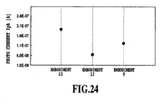
- the photo currents for the ninth embodiment, the twelfth embodiment and the thirteenth embodiment were obtained.
- the results are shown in Fig. 24 .
- the photo current I ph in the twelfth embodiment was reduced by about half. This was because, since the p-type doped InSb layer, which is a light absorption layer, was formed on the AlInSb layer by hetero growth, the crystallinity of the light absorption layer was reduced, and the quantum efficiency dropped.
- the photo current I ph of the thirteenth embodiment was increased about 1.8 times. This was because, of the pairs of electrons and positive holes generated by infrared absorption, the electrons to be diffused toward the p layer were reduced and the photo current was increased. That is, the effects obtained by increasing the external quantum efficiency could be confirmed.
- the structure according to the thirteenth embodiment is a more preferable structure for the unit device of a compound semiconductor infrared sensor.
- a compound semiconductor infrared sensor wherein a plurality of devices were connected in series was prepared using the thin compound semiconductor film having the same structure as in the thirteenth embodiment.
- a step was formed using acid or ion milling to obtain a contact with the n-type doped InSb layers.
- mesa etching, for device separation was performed for the thin compound semiconductor film for which the step was formed.
- the entire surface was covered with an SiN passivation film.
- only the electrode portions of the SiN protective film were opened as windows, Au/Ti was deposited using EB evaporation, and electrodes were formed using the lift off method.
- electrodes were formed so that the InSb layer of a specific device, whereat Sn was doped using 1.0 x 10 19 atoms/cm 3 , was electrically connected to the InSb layer of a device adjacent to the specific device and located on the side whereat the step was formed, whereat Zn was doped using 5.0 x 10 18 atoms/cm 3 .
- the light-receiving area of a prepared unit device was 9 ⁇ m x 9 ⁇ m, and a series connection of 260 unit devices was formed on the GaAs substrate. A cross section of a part of the thus obtained sensor is shown in Fig. 25 .
- the compound semiconductor infrared sensor was irradiated using an infrared radiation, and the open circuit voltage of the device was measured as an output voltage. It should be noted that the sensor temperature during the measurement was room temperature (27°C). An incident infrared radiation was emitted by using a blackbody furnace at 500 K, which was located at a distance of 10 cm from the sensor. With this arrangement, an infrared radiation was emitted, directed toward the substrate side of the sensor. The energy of the incident infrared radiation was 1.2 mW/cm 2 . The frequency for light chopping was 10 Hz, and Si was used as a filter for cutting light, such as visible light.
- the obtained output V out was 91 ⁇ V, and it was confirmed that an output voltage near 100 ⁇ V was obtained at room temperature. The output was remarkably increased compared with when only the unit device was used. These results show an appropriate output for signal processing using an IC. And a microminiature infrared sensor that can be operated at a higher sensitivity, at room temperature, without a cooling mechanism can be provided by combining the compound infrared semiconductor and the infrared sensor IC with the hybrid formation.
- a compound semiconductor infrared sensor with the same structure as in the fourteenth embodiment, and an integrated circuit, wherein an amplification circuit and a chopping circuit, etc., are mounted are arranged in a single package, in a hybrid manner, to obtain an infrared sensor IC.
- the integrated circuit (IC), wherein the amplification circuit, the chopping circuit, etc., are mounted was manufactured using a common CMOS line. Thereafter, using flip-chip bonding, a compound semiconductor infrared sensor according to the fourteenth embodiment was bonded to the IC, i.e., the substrate of the integrated circuit with the substrate of the sensor facing up, so that the electrode portions of the thin compound semiconductor film of the sensor joined the electrode portions of the IC. Further, the electrode portions (lands) in the package were electrically connected to the integrated circuit using wire bonding. In addition, an Si filter was attached to the infrared entry portion of the package, so that an infrared sensor IC for a fifteenth embodiment was completed. A cross section thereof is shown in Fig. 26 .
- reference numeral 32 denotes a compound semiconductor infrared sensor
- reference numeral 33 an integrated circuit
- reference numeral 34 wire bonding
- reference numeral 35 a package
- reference numeral 36 an Si filter
- reference numeral 37 bumps
- reference numeral 38 lands
- reference numeral 39 package electrodes.
- the complete infrared sensor IC is a microminiature infrared sensor IC having an area size of 3 mm x 3 mm and a thickness of 1.2 mm, which is not conventionally produced. Furthermore, according to this structure, an infrared radiation passes through the Si filter 36 and enters from the substrate side of the compound semiconductor sensor 32. Since a semi-insulating GaAs substrate is used, an infrared radiation having a wavelength of 5 ⁇ m or longer is appropriately transmitted through the substrate, and is absorbed by the thin compound semiconductor layer. Thus, the incident infrared radiation can be efficiently fetched as a signal, without being interrupted by the electrodes and the wiring portion of the compound semiconductor infrared sensor 32.
- a characteristic of the infrared sensor IC of the fifteenth embodiment is that, in spite of its being a simple package, it is not easily affected by electromagnetic noise and thermal fluctuation.
- the infrared sensor IC can be appropriately used as a human sensor that detects thermal energy radiated by a person.
- a characteristic of the infrared sensor IC which is a microminiature about the size of an IC chip, is that it is not easily affected by electromagnetic noise and thermal fluctuation, and enables automatic turning on/off of lights and home electrical appliances. Thus, great effects in the saving of energy can be expected.
Landscapes
- Physics & Mathematics (AREA)
- General Physics & Mathematics (AREA)
- Spectroscopy & Molecular Physics (AREA)
- Nanotechnology (AREA)
- Chemical & Material Sciences (AREA)
- Engineering & Computer Science (AREA)
- Biophysics (AREA)
- Optics & Photonics (AREA)
- Crystallography & Structural Chemistry (AREA)
- Life Sciences & Earth Sciences (AREA)
- Light Receiving Elements (AREA)
- Photometry And Measurement Of Optical Pulse Characteristics (AREA)
- Radiation Pyrometers (AREA)
- Thermistors And Varistors (AREA)
Claims (14)
- Infrarotsensor mit:einem Substrat (15); undeinem Verbindungshalbleiterschichtenstapel, der auf besagtem Substrat (15) durch Stapeln einer Mehrzahl von Verbindungshalbleiterschichten ausgebildet ist,bei dem besagter Verbindungshalbleiterschichtenstapeleine n-leitend dotierte Verbindungshalbleiterschicht (16), die auf besagtem Substrat (15) ausgebildet ist und die ein n-leitend dotiertes Material ist, das Indium und Antimon aufweist;eine Verbindungshalbleiterlichtabsorptionsschicht (17), die auf besagter n-leitend dotierter Verbindungshalbleiterschicht (16) ausgebildet ist und die ein nicht-dotiertes oder p-leitend dotiertes Material ist, das Indium und Antimon aufweist; undeine p-leitend dotierte Verbindungshalbleiterschicht (18) aufweist, die auf besagter Verbindungshalbleiterlichtabsorptionsschicht (17) ausgebildet ist und die ein Material ist, das bei einer höheren Trägerdichte als besagte Verbindungshalbleiterlichtabsorptionsschicht (17) p-dotiert ist und eine größere Bandlücke als besagte Verbindungshalbleiterlichtabsorptionsschicht (17) aufweist,dadurch gekennzeichnet, dass besagter Verbindungshalbleiterschichtenstapel ferner eine Verbindungshalbleiterkontaktschicht (21) aufweist, die auf besagter p-leitend dotierter Verbindungshalbleiterschicht (18) ausgebildet ist und die ein Material ist, das Indium und Antimon aufweist, und bei einer Trägerdichte gleich oder größer als die Trägerdichte besagter p-leitend dotierter Verbindungshalbleiterschicht (18) p-leitend dotiert ist und die einen niedrigeren elektrischen Widerstand als den besagter p-leitend dotierter Verbindungshalbleiterschicht (18) aufweist.
- Infrarotsensor nach Anspruch 1, bei dem besagte n-leitend dotierte Verbindungshalbleiterschicht (16) InSb ist, besagte Verbindungshalbleiterlichtabsorptionsschicht (17) eines von InSb, InAsSb und InSbN ist und besagte p-leitend dotierte Verbindungshalbleiterschicht (18) entweder AlInSb oder GaInSb oder eines von AlAs, InAs, GaAs, AlSb und GaSb oder ein Mischkristall von diesen ist.
- Infrarotsensor nach Anspruch 1 oder 2, bei dem ein n-leitender Dotierstoff für besagte n-leitend dotierte Verbindungshalbleiterschicht (16) Sn ist und ein p-leitender Dotierstoff für besagte Verbindungshalbleiterlichtabsorptionsschicht (17) und besagte p-leitend dotierte Verbindungshalbleiterschicht (18) Zn ist.
- Infrarotsensor nach einem der Ansprüche 1 bis 3, bei dem besagte Verbindungshalbleiterkontaktschicht (21) InSb ist.
- Infrarotsensor nach einem der Ansprüche 1 bis 4, bei dem ein p-leitender Dotierstoff für besagte Verbindungshalbleiterkontaktschicht (21) Zn ist.
- Infrarotsensor nach einem der Ansprüche 1 bis 5, bei dem besagtes Substrat (15) ein halbisolierendes Substrat oder ein Substrat ist, so dass besagte n-leitend dotierte Verbindungshalbleiterschicht (16), die auf besagtem Substrat (15) ausgebildet ist, von besagtem Substrat (15) isoliert werden kann, der Infrarotsensor ferner:eine erste Elektrode (19), die in einem Bereich besagter n-leitend dotierter Verbindungshalbleiterschicht (16) ausgebildet ist, wo besagte Haltleiterlichtabsorptionsschicht (17) nicht ausgebildet ist; undeine zweite Elektrode (19) aufweist, die in einem Bereich auf besagter p-leitend dotierter Verbindungshalbleiterschicht (18) ausgebildet ist.
- Infrarotsensor nach Anspruch 6, bei dem eine Mehrzahl besagter Verbindungshalbleiterschichtenstapel angrenzend auf besagtem Substrat (15) ausgebildet sind, so dass eine erste Elektrode (19), die auf einem Verbindungshalbleiterschichtenstapel ausgebildet ist, in Reihe mit einer zweiten Elektrode (19) verbunden ist, die auf einem Verbindungshalbleiterschichtenstapel ausgebildet ist, der an besagten Verbindungshalbleiterschichtenstapel angrenzt, auf dem besagte erste Elektrode (19) ausgebildet ist.
- Infrarotsensor nach Anspruch 6 oder 7, bei dem, wenn ein Ausgabesignal gemessen wird, eine Vorspannung zwischen besagter erster und besagter zweiter Elektrode (19) auf null gesetzt wird, und ein Signal, wenn eine Infrarotstrahlung einfällt, als eine Leerlaufspannung gelesen wird.
- Integrierte Infrarotsensorschaltung (Infrarotsensor-IC) mit:einem Infrarotsensor nach einem der Ansprüche 1 bis 8; undeiner integrierten Schaltung (3) zum Verarbeiten besagten elektrischen Signals, das von besagtem Infrarotsensor ausgegeben wird, zur Durchführung eines vorherbestimmten Vorgangs,bei dem besagter Infrarotsensor und besagte integrierte Schaltung (3) in einem einzelnen Paket in einer Hybridweise angeordnet sind.
- Infrarotsensorherstellungsverfahren mit den Schritten:Ausbilden einer n-leitend dotierten Verbindungshalbleiterschicht (16), die ein n-leitendes Material ist, das Indium und Antimon aufweist, auf einem Substrat (15);Ausbilden einer Verbindungshalbleiterlichtabsorptionsschicht (17), die ein nicht-dotiertes oderp-dotiertes Material ist, das Indium und Antimon aufweist, auf besagter n-leitend dotierter Verbindungshalbleiterschicht (16); undAusbilden einer p-leitend dotierten Verbindungshalbleiterschicht (18), die ein Material ist, das bei einer höheren Trägerdichte als besagte Verbindungshalbleiterlichtabsorptionsschicht (17) p-leitend dotiert ist und eine größere Bandlücke als besagte Verbindungshalbleiterlichtabsorptionsschicht (17) aufweist, auf besagter Verbindungshalbleiterlichtabsorptionsschicht (17),gekennzeichnet durch Ausbilden einer Verbindungshalbleiterkontaktschicht (21), die Indium und Antimon aufweist und bei einer Trägerdichte gleich oder größer als besagte p-leitend dotierte Verbindungshalbleiterschicht (18) p-leitend dotiert ist und einen niedrigeren elektrischen Widerstand als den besagter p-leitend dotierter Verbindungshalbleiterschicht (18) aufweist, auf besagter p-leitend dotierter Verbindungshalbleiterschicht (18).
- Infrarotsensorherstellungsverfahren nach Anspruch 10, bei dem besagte n-leitend dotierte Verbindungshalbleiterschicht (16) InSb ist, besagte Verbindungshalbleiterlichtabsorptionsschicht (17) eines von InSb, InAsSb und InSbN ist und besagte p-leitend dotierte Verbindungshalbleiterschicht (18) entweder AlInSb oder GaInSb oder eines von AlAs, InAs, GaAs, AlSb und GaSb oder ein Mischkristall von diesen ist.
- Infrarotsensorherstellungsverfahren nach Anspruch 10 oder 11, bei dem ein n-leitender Dotierstoff für besagte n-leitend dotierte Verbindungshalbleiterschicht (16) Sn ist und ein p-leitender Dotierstoff für besagte Verbindungshalbleiterlichtabsorptionsschicht (17) und besagte p-leitend dotierte Verbindungshalbleiterschicht (18) Zn ist.
- Infrarotsensorherstellungsverfahren nach einem der Ansprüche 10 bis 12, bei dem besagte Verbindungshalbleiterkontaktschicht (21) InSb ist.
- Infrarotsensorherstellungsverfahren nach einem der Ansprüche 10 bis 13, bei dem ein p-leitender Dotierstoff für besagte Verbindungshalbleiterkontaktschicht (21) Zn ist.
Applications Claiming Priority (2)
| Application Number | Priority Date | Filing Date | Title |
|---|---|---|---|
| JP2003316281 | 2003-09-09 | ||
| EP04787821A EP1667239A4 (de) | 2003-09-09 | 2004-09-09 | Infrarot-sensor-ic, infrarot-sensor und herstellungsverfahren dafür |
Related Parent Applications (2)
| Application Number | Title | Priority Date | Filing Date |
|---|---|---|---|
| EP04787821A Division EP1667239A4 (de) | 2003-09-09 | 2004-09-09 | Infrarot-sensor-ic, infrarot-sensor und herstellungsverfahren dafür |
| EP04787821.0 Division | 2004-09-09 |
Publications (4)
| Publication Number | Publication Date |
|---|---|
| EP2023398A2 EP2023398A2 (de) | 2009-02-11 |
| EP2023398A3 EP2023398A3 (de) | 2011-04-13 |
| EP2023398B1 EP2023398B1 (de) | 2014-10-22 |
| EP2023398B9 true EP2023398B9 (de) | 2015-02-18 |
Family
ID=34308443
Family Applications (2)
| Application Number | Title | Priority Date | Filing Date |
|---|---|---|---|
| EP08019935.9A Expired - Lifetime EP2023398B9 (de) | 2003-09-09 | 2004-09-09 | Infrarotsensor-IC und Infrarotsensor und Herstellungsverfahren dafür |
| EP04787821A Withdrawn EP1667239A4 (de) | 2003-09-09 | 2004-09-09 | Infrarot-sensor-ic, infrarot-sensor und herstellungsverfahren dafür |
Family Applications After (1)
| Application Number | Title | Priority Date | Filing Date |
|---|---|---|---|
| EP04787821A Withdrawn EP1667239A4 (de) | 2003-09-09 | 2004-09-09 | Infrarot-sensor-ic, infrarot-sensor und herstellungsverfahren dafür |
Country Status (7)
| Country | Link |
|---|---|
| US (2) | US7768048B2 (de) |
| EP (2) | EP2023398B9 (de) |
| JP (1) | JP4086875B2 (de) |
| KR (1) | KR100762772B1 (de) |
| CN (2) | CN101459203B (de) |
| TW (1) | TWI261934B (de) |
| WO (1) | WO2005027228A1 (de) |
Cited By (1)
| Publication number | Priority date | Publication date | Assignee | Title |
|---|---|---|---|---|
| RU199226U1 (ru) * | 2019-11-19 | 2020-08-24 | Общество с ограниченной ответственностью "ИоффеЛЕД" | Двухспектральный фотодиод для средневолнового инфракрасного излучения |
Families Citing this family (75)
| Publication number | Priority date | Publication date | Assignee | Title |
|---|---|---|---|---|
| GB0411926D0 (en) * | 2004-05-27 | 2004-06-30 | Isis Innovation | Direct electron detector |
| US7791014B2 (en) * | 2005-03-09 | 2010-09-07 | Asahi Kasei Emd Corporation | Optical device and a method of manufacturing an optical device having a photoelectric conversion element and an optical adjustment element |
| JP2007081225A (ja) * | 2005-09-15 | 2007-03-29 | Asahi Kasei Electronics Co Ltd | 赤外線センサ、および、その製造方法 |
| DE102005061206B4 (de) * | 2005-09-30 | 2019-10-17 | Osram Opto Semiconductors Gmbh | Verwendung einer Detektoranordnung als Umgebungslichtsensor |
| JP4802242B2 (ja) * | 2006-04-24 | 2011-10-26 | 旭化成エレクトロニクス株式会社 | 赤外線センサ |
| JP5063929B2 (ja) * | 2006-04-28 | 2012-10-31 | 旭化成エレクトロニクス株式会社 | 赤外線センサ |
| JP2008066584A (ja) * | 2006-09-08 | 2008-03-21 | Asahi Kasei Electronics Co Ltd | 光センサ |
| JP5290505B2 (ja) * | 2006-09-08 | 2013-09-18 | 旭化成エレクトロニクス株式会社 | 光センサの製造方法 |
| US8044435B2 (en) | 2006-11-14 | 2011-10-25 | Lockheed Martin Corporation | Sub-pixel nBn detector |
| WO2008066118A1 (ja) * | 2006-11-30 | 2008-06-05 | Asahi Kasei Kabushiki Kaisha | 薄膜積層体及びそれを用いた薄膜磁気センサ並びにその製造方法 |
| US8125060B2 (en) | 2006-12-08 | 2012-02-28 | Infineon Technologies Ag | Electronic component with layered frame |
| GB2452992A (en) * | 2007-09-24 | 2009-03-25 | Selex Sensors & Airborne Sys | Dual band infrared photodetector |
| KR100921693B1 (ko) * | 2007-10-23 | 2009-10-15 | 한국과학기술연구원 | In(As)Sb 반도체의 격자 부정합 기판상 제조방법 및이를 이용한 반도체 소자 |
| JP2009206357A (ja) * | 2008-02-28 | 2009-09-10 | Asahi Kasei Electronics Co Ltd | 化合物半導体装置及び化合物半導体装置の製造方法 |
| TWI427824B (zh) * | 2008-03-14 | 2014-02-21 | 旭化成電子材料元件股份有限公司 | 紅外線發光元件 |
| JP4922979B2 (ja) * | 2008-03-28 | 2012-04-25 | 旭化成エレクトロニクス株式会社 | 半導体基板 |
| JP5266521B2 (ja) * | 2008-03-31 | 2013-08-21 | 旭化成エレクトロニクス株式会社 | 赤外線センサ、及び赤外線センサic |
| CN102057495B (zh) * | 2008-06-04 | 2013-10-09 | 旭化成微电子株式会社 | 量子型红外线传感器以及使用该量子型红外线传感器的量子型红外线气体浓度仪 |
| TWI422018B (zh) * | 2008-08-20 | 2014-01-01 | 原相科技股份有限公司 | 感測模組 |
| WO2010036956A1 (en) * | 2008-09-25 | 2010-04-01 | California Institute Of Technology | High operating temperature barrier infrared detector with tailorable cutoff wavelength |
| US20120104460A1 (en) | 2010-11-03 | 2012-05-03 | Alta Devices, Inc. | Optoelectronic devices including heterojunction |
| WO2010048547A2 (en) | 2008-10-23 | 2010-04-29 | Alta Devices, Inc. | Photovoltaic device with increased light trapping |
| US8674214B2 (en) | 2008-10-23 | 2014-03-18 | Alta Devices, Inc. | Thin absorber layer of a photovoltaic device |
| KR20110086098A (ko) | 2008-10-23 | 2011-07-27 | 알타 디바이씨즈, 인크. | 광전지 장치 |
| WO2010077984A2 (en) * | 2008-12-16 | 2010-07-08 | California Institute Of Technology | Digital alloy absorber for photodetectors |
| JP2010272577A (ja) * | 2009-05-19 | 2010-12-02 | Takehisa Sasaki | 放射線検出素子、及び、放射線検出装置 |
| US8653460B2 (en) * | 2009-05-28 | 2014-02-18 | Technion Research & Development Foundation Limited | Method and system for detecting light |
| US9691921B2 (en) | 2009-10-14 | 2017-06-27 | Alta Devices, Inc. | Textured metallic back reflector |
| US20150380576A1 (en) | 2010-10-13 | 2015-12-31 | Alta Devices, Inc. | Optoelectronic device with dielectric layer and method of manufacture |
| US9502594B2 (en) | 2012-01-19 | 2016-11-22 | Alta Devices, Inc. | Thin-film semiconductor optoelectronic device with textured front and/or back surface prepared from template layer and etching |
| US11271128B2 (en) | 2009-10-23 | 2022-03-08 | Utica Leaseco, Llc | Multi-junction optoelectronic device |
| US9768329B1 (en) | 2009-10-23 | 2017-09-19 | Alta Devices, Inc. | Multi-junction optoelectronic device |
| US20170141256A1 (en) | 2009-10-23 | 2017-05-18 | Alta Devices, Inc. | Multi-junction optoelectronic device with group iv semiconductor as a bottom junction |
| KR20120085916A (ko) * | 2009-11-16 | 2012-08-01 | 루돌프 테크놀로지스 인코퍼레이티드 | 본딩된 기판의 적외선 검사 |
| JP5731754B2 (ja) * | 2010-02-18 | 2015-06-10 | 旭化成エレクトロニクス株式会社 | 赤外線センサ |
| IL211339A (en) * | 2010-02-21 | 2015-05-31 | Technion Res & Dev Foundation | Light detection and manufacturing method |
| US8367450B2 (en) | 2010-02-21 | 2013-02-05 | Technion Research & Development Foundation Ltd. | Light emitting system and method of fabricating and using the same |
| US8552479B2 (en) * | 2010-03-12 | 2013-10-08 | Flir Systems, Inc. | Aluminum indium antimonide focal plane array |
| US8552480B2 (en) | 2010-03-12 | 2013-10-08 | Flir Systems, Inc. | Aluminum indium antimonide focal plane array |
| JP2011216706A (ja) * | 2010-03-31 | 2011-10-27 | Asahi Kasei Electronics Co Ltd | 赤外線センサ |
| JP5589605B2 (ja) * | 2010-06-25 | 2014-09-17 | セイコーエプソン株式会社 | 焦電型検出器、焦電型検出装置及び電子機器 |
| JP2012146806A (ja) * | 2011-01-12 | 2012-08-02 | Irspec Corp | 格子不整合赤外化合物半導体受光素子 |
| JP5606374B2 (ja) * | 2011-03-29 | 2014-10-15 | 旭化成エレクトロニクス株式会社 | 量子型赤外線センサ用化合物半導体積層体の製造方法および量子型赤外線センサ |
| JP5706217B2 (ja) * | 2011-03-31 | 2015-04-22 | 旭化成エレクトロニクス株式会社 | 赤外線センサ |
| US11038080B2 (en) | 2012-01-19 | 2021-06-15 | Utica Leaseco, Llc | Thin-film semiconductor optoelectronic device with textured front and/or back surface prepared from etching |
| JP5859364B2 (ja) * | 2012-03-30 | 2016-02-10 | 旭化成エレクトロニクス株式会社 | 受光強度演算デバイス及び位置検出デバイス |
| US9046410B2 (en) | 2012-03-29 | 2015-06-02 | Asahi Kasei Microdevices Corporation | Light receiving device |
| JP5917233B2 (ja) * | 2012-03-30 | 2016-05-11 | 旭化成エレクトロニクス株式会社 | 受光強度演算デバイス及び位置検出デバイス |
| US8952480B2 (en) | 2012-09-13 | 2015-02-10 | Stmicroelectronics Asia Pacific Pte. Ltd. | Electronic device including thermal sensor and peltier cooler and related methods |
| US9276159B2 (en) * | 2012-12-21 | 2016-03-01 | Teledyne Scientific & Imaging, Llc | Superlattice structure |
| JP2014146771A (ja) * | 2013-01-30 | 2014-08-14 | Asahi Kasei Electronics Co Ltd | 赤外線センサ |
| KR102123991B1 (ko) * | 2013-03-11 | 2020-06-17 | 삼성전자주식회사 | 반도체 패키지 및 이를 구비하는 전자 시스템 |
| JP2014178172A (ja) * | 2013-03-14 | 2014-09-25 | Omron Corp | 赤外線センサおよびその製造方法 |
| WO2014156123A1 (ja) * | 2013-03-25 | 2014-10-02 | 旭化成エレクトロニクス株式会社 | 化合物半導体積層体及び半導体装置 |
| US9196769B2 (en) | 2013-06-25 | 2015-11-24 | L-3 Communications Cincinnati Electronics Corporation | Superlattice structures and infrared detector devices incorporating the same |
| JP2015122441A (ja) * | 2013-12-24 | 2015-07-02 | 京セミ株式会社 | 受光素子及び光電変換回路 |
| CN103779457A (zh) * | 2014-02-14 | 2014-05-07 | 中国科学院上海微系统与信息技术研究所 | 一种可获得极宽短波红外发光谱的半导体材料及其制备方法 |
| US10014424B2 (en) | 2014-03-13 | 2018-07-03 | Raytheon Company | Reduced junction area barrier-based photodetector |
| CN104977027B (zh) * | 2015-05-29 | 2017-06-13 | 江阴苏阳电子股份有限公司 | 基于mcm‑3d封装的微型智能传感器 |
| JP6764705B2 (ja) * | 2016-02-10 | 2020-10-07 | 旭化成エレクトロニクス株式会社 | 赤外線受光素子 |
| JP6908367B2 (ja) * | 2016-10-19 | 2021-07-28 | 旭化成エレクトロニクス株式会社 | 赤外線発光素子 |
| JP6969199B2 (ja) * | 2017-08-03 | 2021-11-24 | 住友電気工業株式会社 | 受光素子 |
| WO2019040486A1 (en) * | 2017-08-24 | 2019-02-28 | Board Of Regents, The University Of Texas System | MEDIUM INFRARED DETECTOR USING HIGHLY DOPED REAR PANEL FOR SENSOR STRUCTURE |
| JP6917352B2 (ja) | 2018-01-18 | 2021-08-11 | 旭化成エレクトロニクス株式会社 | 赤外線検出素子 |
| US11935973B2 (en) | 2018-02-28 | 2024-03-19 | Asahi Kasei Microdevices Corporation | Infrared detecting device |
| JP7096684B2 (ja) * | 2018-03-23 | 2022-07-06 | 旭化成エレクトロニクス株式会社 | 赤外線発光素子 |
| TWI661571B (zh) * | 2018-07-06 | 2019-06-01 | 王俊凱 | 砷化鎵之帶通型紅光與紅外光檢測器 |
| WO2021062436A1 (en) * | 2019-09-27 | 2021-04-01 | The Procter & Gamble Company | Systems and methods for thermal radiation detection |
| US11592336B2 (en) | 2019-09-27 | 2023-02-28 | The Procter & Gamble Company | Systems and methods for thermal radiation detection |
| JP2021144966A (ja) | 2020-03-10 | 2021-09-24 | 旭化成エレクトロニクス株式会社 | 赤外線検出素子 |
| JP7505320B2 (ja) * | 2020-08-13 | 2024-06-25 | 富士通株式会社 | 2波長光検出器、及びこれを用いたイメージセンサ |
| CN112186070B (zh) * | 2020-09-01 | 2022-04-19 | 中国电子科技集团公司第十一研究所 | 一种红外探测器件制备方法 |
| CN113629164B (zh) * | 2021-08-10 | 2024-04-12 | 苏州矩阵光电有限公司 | 下入光式红外传感器元件及其制造方法 |
| CN113644158B (zh) * | 2021-08-10 | 2024-04-12 | 苏州矩阵光电有限公司 | 上入光式红外传感器元件及其制造方法 |
| JP7719496B2 (ja) * | 2021-11-25 | 2025-08-06 | 国立研究開発法人物質・材料研究機構 | 赤外線検出素子、その製造方法、および赤外線検出装置 |
Family Cites Families (38)
| Publication number | Priority date | Publication date | Assignee | Title |
|---|---|---|---|---|
| CA1081835A (en) | 1976-11-08 | 1980-07-15 | Dieter H. Pommerrenig | Method of producing a semiconductor photodiode of indium antimonide and device thereof |
| US4599632A (en) * | 1982-08-30 | 1986-07-08 | At&T Bell Laboratories | Photodetector with graded bandgap region |
| GB8417303D0 (en) * | 1984-07-06 | 1984-08-08 | Secr Defence | Infra-red detector |
| US5455421A (en) * | 1985-08-13 | 1995-10-03 | Massachusetts Institute Of Technology | Infrared detector using a resonant optical cavity for enhanced absorption |
| JPS62257773A (ja) | 1986-05-01 | 1987-11-10 | Toshiba Corp | 光半導体素子およびその製造方法 |
| JPS62272564A (ja) | 1986-05-20 | 1987-11-26 | Fujitsu Ltd | 赤外線検知装置 |
| JPS63308970A (ja) | 1987-06-11 | 1988-12-16 | Nikon Corp | ハイブリッド型赤外線検出装置 |
| EP0345343B1 (de) | 1987-11-23 | 1993-08-25 | Santa Barbara Research Center | Verfahren und vorrichtung zur detektion von infrarotstrahlung |
| US4970567A (en) * | 1987-11-23 | 1990-11-13 | Santa Barbara Research Center | Method and apparatus for detecting infrared radiation |
| JP2827414B2 (ja) | 1990-03-15 | 1998-11-25 | 富士通株式会社 | 半導体装置 |
| JPH0453271A (ja) * | 1990-06-21 | 1992-02-20 | Toshiba Corp | 半導体装置の製造方法 |
| EP0473125B1 (de) * | 1990-08-30 | 1996-01-31 | Shimadzu Corporation | Strahlungsdetektor |
| US5227656A (en) | 1990-11-06 | 1993-07-13 | Cincinnati Electronics Corporation | Electro-optical detector array |
| US5646437A (en) * | 1991-08-08 | 1997-07-08 | Santa Barbara Research Center | Indium antimonide (InSb) photodetector device and structure for infrared, visible and ultraviolet radiation |
| JPH05160429A (ja) * | 1991-12-09 | 1993-06-25 | Nec Corp | 赤外線検知器 |
| JPH05190846A (ja) * | 1992-01-09 | 1993-07-30 | Hitachi Cable Ltd | 電界効果型トランジスタ |
| JPH0777270B2 (ja) | 1992-12-24 | 1995-08-16 | 日本電気株式会社 | 赤外線検出器 |
| JPH0794774A (ja) | 1993-09-22 | 1995-04-07 | Honda Motor Co Ltd | 半導体光検出装置およびイメージセンサ |
| US5483088A (en) * | 1994-08-12 | 1996-01-09 | S.R.I. International | Compounds and infrared devices including In1-x Tlx Q, where Q is As1-y Py and 0≦y≦1 |
| JP3468866B2 (ja) * | 1994-09-16 | 2003-11-17 | 富士通株式会社 | 3次元量子閉じ込めを利用した半導体装置 |
| JPH08139355A (ja) | 1994-11-08 | 1996-05-31 | Nec Corp | 半導体受光素子 |
| JPH10284762A (ja) * | 1995-02-16 | 1998-10-23 | Asahi Chem Ind Co Ltd | 表面弾性波を増幅するための積層構造及び増幅器 |
| US5650635A (en) * | 1995-07-14 | 1997-07-22 | Northwestern University | Multiple stacked Sb-based heterostructures |
| US5959340A (en) * | 1995-09-05 | 1999-09-28 | Drs Technologies, Inc. | Thermoplastic mounting of a semiconductor die to a substrate having a mismatched coefficient of thermal expansion |
| JPH09237889A (ja) | 1996-02-29 | 1997-09-09 | Hitachi Ltd | 半導体結晶積層体及びそれを用いた半導体装置 |
| US5799026A (en) * | 1996-11-01 | 1998-08-25 | The United States Of America As Represented By The Secretary Of The Navy | Interband quantum well cascade laser, with a blocking quantum well for improved quantum efficiency |
| JPH10233523A (ja) | 1997-02-18 | 1998-09-02 | Hamamatsu Photonics Kk | 光検出器 |
| JP3362858B2 (ja) * | 1997-02-28 | 2003-01-07 | 旭化成電子株式会社 | 磁気センサ |
| US6037614A (en) * | 1997-03-07 | 2000-03-14 | California Institute Of Technology | Methods for manufacturing group IV element alloy semiconductor materials and devices that include such materials |
| FR2775388B1 (fr) * | 1998-02-26 | 2001-12-07 | Sagem | Alliage a base d'indium et transducteur infrarouge utilisant un tel alliage |
| JP2000208830A (ja) | 1999-01-11 | 2000-07-28 | Hitachi Cable Ltd | 化合物半導体多層薄膜及び磁気センサ |
| JP2000269537A (ja) | 1999-03-15 | 2000-09-29 | New Japan Radio Co Ltd | 半導体受光装置 |
| US6992319B2 (en) * | 2000-07-18 | 2006-01-31 | Epitaxial Technologies | Ultra-linear multi-channel field effect transistor |
| JP2002313815A (ja) * | 2001-04-12 | 2002-10-25 | Hitachi Ltd | 電界効果トランジスタ及び高周波モジュール |
| US20030189234A1 (en) * | 2002-04-09 | 2003-10-09 | Johnson Mark B. | Hall effect device |
| US6646315B1 (en) * | 2002-04-22 | 2003-11-11 | The United States Of America As Represented By The Secretary Of The Navy | Conductive film layer for hall effect device |
| US6683359B2 (en) * | 2002-06-21 | 2004-01-27 | The United States Of America As Represented By The Secretary Of The Navy | Hall effect device with multiple layers |
| JP3954478B2 (ja) * | 2002-11-06 | 2007-08-08 | 浜松ホトニクス株式会社 | 半導体光電陰極、及びそれを用いた光電管 |
-
2004
- 2004-09-09 CN CN2008101795852A patent/CN101459203B/zh not_active Expired - Fee Related
- 2004-09-09 JP JP2005513897A patent/JP4086875B2/ja not_active Expired - Lifetime
- 2004-09-09 KR KR1020067004857A patent/KR100762772B1/ko not_active Expired - Fee Related
- 2004-09-09 EP EP08019935.9A patent/EP2023398B9/de not_active Expired - Lifetime
- 2004-09-09 US US10/571,287 patent/US7768048B2/en active Active
- 2004-09-09 TW TW093127417A patent/TWI261934B/zh active
- 2004-09-09 EP EP04787821A patent/EP1667239A4/de not_active Withdrawn
- 2004-09-09 WO PCT/JP2004/013158 patent/WO2005027228A1/ja not_active Ceased
- 2004-09-09 CN CNB2004800259720A patent/CN100511719C/zh not_active Expired - Fee Related
-
2010
- 2010-06-22 US US12/801,718 patent/US20100264459A1/en not_active Abandoned
Cited By (1)
| Publication number | Priority date | Publication date | Assignee | Title |
|---|---|---|---|---|
| RU199226U1 (ru) * | 2019-11-19 | 2020-08-24 | Общество с ограниченной ответственностью "ИоффеЛЕД" | Двухспектральный фотодиод для средневолнового инфракрасного излучения |
Also Published As
| Publication number | Publication date |
|---|---|
| EP1667239A4 (de) | 2008-08-06 |
| KR20060083206A (ko) | 2006-07-20 |
| EP1667239A1 (de) | 2006-06-07 |
| CN101459203B (zh) | 2011-06-15 |
| JP4086875B2 (ja) | 2008-05-14 |
| KR100762772B1 (ko) | 2007-10-02 |
| CN100511719C (zh) | 2009-07-08 |
| TW200515610A (en) | 2005-05-01 |
| US20100264459A1 (en) | 2010-10-21 |
| EP2023398B1 (de) | 2014-10-22 |
| WO2005027228A1 (ja) | 2005-03-24 |
| CN1853281A (zh) | 2006-10-25 |
| US20070090337A1 (en) | 2007-04-26 |
| US7768048B2 (en) | 2010-08-03 |
| EP2023398A2 (de) | 2009-02-11 |
| JPWO2005027228A1 (ja) | 2008-06-12 |
| CN101459203A (zh) | 2009-06-17 |
| EP2023398A3 (de) | 2011-04-13 |
| TWI261934B (en) | 2006-09-11 |
Similar Documents
| Publication | Publication Date | Title |
|---|---|---|
| EP2023398B9 (de) | Infrarotsensor-IC und Infrarotsensor und Herstellungsverfahren dafür | |
| EP2756523B1 (de) | Infrarotlichtdetektorvorrichtung mit vorderseitig beleuchteter barriere sowie herstellungsverfahren dafür | |
| JP5528882B2 (ja) | 赤外線センサ | |
| WO2005038997A2 (en) | Intersubband detector with avalanche multiplier region | |
| US7750285B2 (en) | Optical sensor including photoconductive material and carbon nanotube | |
| JP5266521B2 (ja) | 赤外線センサ、及び赤外線センサic | |
| JP2008103742A (ja) | 赤外線センサic | |
| Kim et al. | Room temperature far infrared (8/spl sim/10 μm) photodetectors using self-assembled InAs quantum dots with high detectivity | |
| US9647155B1 (en) | Long wave photo-detection device for used in long wave infrared detection, materials, and method of fabrication | |
| Krier et al. | A room temperature photovoltaic detector for the mid-infrared (1.8-3.4 m) wavelength region | |
| JP5063929B2 (ja) | 赤外線センサ | |
| JP4138853B2 (ja) | 赤外線センサic | |
| Kumar et al. | Mid-Infrared photodetectors based on lattice matched SiGeSn/GeSn heterojunction bipolar transistor with an i-GeSn absorber layer | |
| Kuze et al. | High performance miniaturized InSb photovoltaic infrared sensors operating at room temperature | |
| Camargo et al. | Miniaturized InSb photovoltaic infrared sensor operating at room temperature | |
| Camargo et al. | High-sensitivity temperature measurement with miniaturized InSb mid-IR sensor | |
| KR102609012B1 (ko) | 적외선 감지 소자 | |
| Chen et al. | Breaking the material-limited temperature coefficient of resistance via carrier feedback in a single transistor | |
| Avishan | Identification and characterization of traps in InGaAs short wavelength infrared photodetectors by deep level transient spectroscopy | |
| Kuze et al. | Development of uncooled miniaturized InSb photovoltaic infrared sensors for temperature measurements | |
| Ueno et al. | A novel InSb photodiode infrared sensor operating at room temperature | |
| Camargo et al. | Miniaturized InSb photovoltaic infrared sensor operating at room temperature | |
| Myers et al. | Photoconductive gain in barrier heterostructure infrared detectors | |
| JP5840408B2 (ja) | 赤外線センサ | |
| Ersagun | Dark Current Mechanisms and Passivation of InAsSb Infrared Photodiodes on Alternative Substrates |
Legal Events
| Date | Code | Title | Description |
|---|---|---|---|
| PUAI | Public reference made under article 153(3) epc to a published international application that has entered the european phase |
Free format text: ORIGINAL CODE: 0009012 |
|
| AC | Divisional application: reference to earlier application |
Ref document number: 1667239 Country of ref document: EP Kind code of ref document: P |
|
| AK | Designated contracting states |
Kind code of ref document: A2 Designated state(s): DE FR GB |
|
| REG | Reference to a national code |
Ref country code: DE Ref legal event code: R079 Ref document number: 602004046048 Country of ref document: DE Free format text: PREVIOUS MAIN CLASS: H01L0031035200 Ipc: H01L0031030400 |
|
| PUAL | Search report despatched |
Free format text: ORIGINAL CODE: 0009013 |
|
| AK | Designated contracting states |
Kind code of ref document: A3 Designated state(s): DE FR GB |
|
| RIC1 | Information provided on ipc code assigned before grant |
Ipc: H01L 31/0304 20060101AFI20110308BHEP Ipc: H01L 27/144 20060101ALI20110308BHEP Ipc: H01L 31/0203 20060101ALI20110308BHEP |
|
| 17P | Request for examination filed |
Effective date: 20110805 |
|
| AKX | Designation fees paid |
Designated state(s): DE FR GB |
|
| GRAP | Despatch of communication of intention to grant a patent |
Free format text: ORIGINAL CODE: EPIDOSNIGR1 |
|
| INTG | Intention to grant announced |
Effective date: 20140612 |
|
| GRAS | Grant fee paid |
Free format text: ORIGINAL CODE: EPIDOSNIGR3 |
|
| GRAA | (expected) grant |
Free format text: ORIGINAL CODE: 0009210 |
|
| AC | Divisional application: reference to earlier application |
Ref document number: 1667239 Country of ref document: EP Kind code of ref document: P |
|
| AK | Designated contracting states |
Kind code of ref document: B1 Designated state(s): DE FR GB |
|
| REG | Reference to a national code |
Ref country code: GB Ref legal event code: FG4D |
|
| REG | Reference to a national code |
Ref country code: DE Ref legal event code: R096 Ref document number: 602004046048 Country of ref document: DE Effective date: 20141204 |
|
| REG | Reference to a national code |
Ref country code: DE Ref legal event code: R097 Ref document number: 602004046048 Country of ref document: DE |
|
| PLBE | No opposition filed within time limit |
Free format text: ORIGINAL CODE: 0009261 |
|
| STAA | Information on the status of an ep patent application or granted ep patent |
Free format text: STATUS: NO OPPOSITION FILED WITHIN TIME LIMIT |
|
| 26N | No opposition filed |
Effective date: 20150723 |
|
| REG | Reference to a national code |
Ref country code: FR Ref legal event code: ST Effective date: 20160531 |
|
| PG25 | Lapsed in a contracting state [announced via postgrant information from national office to epo] |
Ref country code: FR Free format text: LAPSE BECAUSE OF NON-PAYMENT OF DUE FEES Effective date: 20150930 |
|
| PGFP | Annual fee paid to national office [announced via postgrant information from national office to epo] |
Ref country code: DE Payment date: 20170905 Year of fee payment: 14 Ref country code: GB Payment date: 20170906 Year of fee payment: 14 |
|
| REG | Reference to a national code |
Ref country code: DE Ref legal event code: R119 Ref document number: 602004046048 Country of ref document: DE |
|
| GBPC | Gb: european patent ceased through non-payment of renewal fee |
Effective date: 20180909 |
|
| PG25 | Lapsed in a contracting state [announced via postgrant information from national office to epo] |
Ref country code: DE Free format text: LAPSE BECAUSE OF NON-PAYMENT OF DUE FEES Effective date: 20190402 |
|
| PG25 | Lapsed in a contracting state [announced via postgrant information from national office to epo] |
Ref country code: GB Free format text: LAPSE BECAUSE OF NON-PAYMENT OF DUE FEES Effective date: 20180909 |