EP1995769A1 - Exposure method and exposure apparatus, stage unit, and device manufacturing method - Google Patents
Exposure method and exposure apparatus, stage unit, and device manufacturing method Download PDFInfo
- Publication number
- EP1995769A1 EP1995769A1 EP08163444A EP08163444A EP1995769A1 EP 1995769 A1 EP1995769 A1 EP 1995769A1 EP 08163444 A EP08163444 A EP 08163444A EP 08163444 A EP08163444 A EP 08163444A EP 1995769 A1 EP1995769 A1 EP 1995769A1
- Authority
- EP
- European Patent Office
- Prior art keywords
- stage
- wafer
- exposure
- substrate
- unit
- Prior art date
- Legal status (The legal status is an assumption and is not a legal conclusion. Google has not performed a legal analysis and makes no representation as to the accuracy of the status listed.)
- Withdrawn
Links
Images


Classifications
-
- H—ELECTRICITY
- H01—ELECTRIC ELEMENTS
- H01L—SEMICONDUCTOR DEVICES NOT COVERED BY CLASS H10
- H01L21/00—Processes or apparatus adapted for the manufacture or treatment of semiconductor or solid state devices or of parts thereof
- H01L21/02—Manufacture or treatment of semiconductor devices or of parts thereof
- H01L21/027—Making masks on semiconductor bodies for further photolithographic processing not provided for in group H01L21/18 or H01L21/34
- H01L21/0271—Making masks on semiconductor bodies for further photolithographic processing not provided for in group H01L21/18 or H01L21/34 comprising organic layers
- H01L21/0273—Making masks on semiconductor bodies for further photolithographic processing not provided for in group H01L21/18 or H01L21/34 comprising organic layers characterised by the treatment of photoresist layers
-
- G—PHYSICS
- G03—PHOTOGRAPHY; CINEMATOGRAPHY; ANALOGOUS TECHNIQUES USING WAVES OTHER THAN OPTICAL WAVES; ELECTROGRAPHY; HOLOGRAPHY
- G03F—PHOTOMECHANICAL PRODUCTION OF TEXTURED OR PATTERNED SURFACES, e.g. FOR PRINTING, FOR PROCESSING OF SEMICONDUCTOR DEVICES; MATERIALS THEREFOR; ORIGINALS THEREFOR; APPARATUS SPECIALLY ADAPTED THEREFOR
- G03F7/00—Photomechanical, e.g. photolithographic, production of textured or patterned surfaces, e.g. printing surfaces; Materials therefor, e.g. comprising photoresists; Apparatus specially adapted therefor
- G03F7/70—Microphotolithographic exposure; Apparatus therefor
- G03F7/70691—Handling of masks or workpieces
- G03F7/70716—Stages
-
- G—PHYSICS
- G03—PHOTOGRAPHY; CINEMATOGRAPHY; ANALOGOUS TECHNIQUES USING WAVES OTHER THAN OPTICAL WAVES; ELECTROGRAPHY; HOLOGRAPHY
- G03F—PHOTOMECHANICAL PRODUCTION OF TEXTURED OR PATTERNED SURFACES, e.g. FOR PRINTING, FOR PROCESSING OF SEMICONDUCTOR DEVICES; MATERIALS THEREFOR; ORIGINALS THEREFOR; APPARATUS SPECIALLY ADAPTED THEREFOR
- G03F7/00—Photomechanical, e.g. photolithographic, production of textured or patterned surfaces, e.g. printing surfaces; Materials therefor, e.g. comprising photoresists; Apparatus specially adapted therefor
- G03F7/20—Exposure; Apparatus therefor
- G03F7/2002—Exposure; Apparatus therefor with visible light or UV light, through an original having an opaque pattern on a transparent support, e.g. film printing, projection printing; by reflection of visible or UV light from an original such as a printed image
- G03F7/2004—Exposure; Apparatus therefor with visible light or UV light, through an original having an opaque pattern on a transparent support, e.g. film printing, projection printing; by reflection of visible or UV light from an original such as a printed image characterised by the use of a particular light source, e.g. fluorescent lamps or deep UV light
-
- G—PHYSICS
- G03—PHOTOGRAPHY; CINEMATOGRAPHY; ANALOGOUS TECHNIQUES USING WAVES OTHER THAN OPTICAL WAVES; ELECTROGRAPHY; HOLOGRAPHY
- G03F—PHOTOMECHANICAL PRODUCTION OF TEXTURED OR PATTERNED SURFACES, e.g. FOR PRINTING, FOR PROCESSING OF SEMICONDUCTOR DEVICES; MATERIALS THEREFOR; ORIGINALS THEREFOR; APPARATUS SPECIALLY ADAPTED THEREFOR
- G03F7/00—Photomechanical, e.g. photolithographic, production of textured or patterned surfaces, e.g. printing surfaces; Materials therefor, e.g. comprising photoresists; Apparatus specially adapted therefor
- G03F7/70—Microphotolithographic exposure; Apparatus therefor
- G03F7/70691—Handling of masks or workpieces
- G03F7/70733—Handling masks and workpieces, e.g. exchange of workpiece or mask, transport of workpiece or mask
-
- G—PHYSICS
- G03—PHOTOGRAPHY; CINEMATOGRAPHY; ANALOGOUS TECHNIQUES USING WAVES OTHER THAN OPTICAL WAVES; ELECTROGRAPHY; HOLOGRAPHY
- G03F—PHOTOMECHANICAL PRODUCTION OF TEXTURED OR PATTERNED SURFACES, e.g. FOR PRINTING, FOR PROCESSING OF SEMICONDUCTOR DEVICES; MATERIALS THEREFOR; ORIGINALS THEREFOR; APPARATUS SPECIALLY ADAPTED THEREFOR
- G03F7/00—Photomechanical, e.g. photolithographic, production of textured or patterned surfaces, e.g. printing surfaces; Materials therefor, e.g. comprising photoresists; Apparatus specially adapted therefor
- G03F7/70—Microphotolithographic exposure; Apparatus therefor
- G03F7/708—Construction of apparatus, e.g. environment aspects, hygiene aspects or materials
- G03F7/7085—Detection arrangement, e.g. detectors of apparatus alignment possibly mounted on wafers, exposure dose, photo-cleaning flux, stray light, thermal load
Definitions
- processing is repeatedly performed in three steps, which are a wafer exchange step where a wafer is exchanged on the wafer stage, a wafer alignment step for accurately obtaining the position of each shot area on the wafer, and an exposure step where the pattern formed on a reticle (or a mask) is transferred onto each shot area of the wafer while controlling the position of the wafer stage based on the wafer alignment results, using one wafer stage.
- a wafer exchange step where a wafer is exchanged on the wafer stage
- a wafer alignment step for accurately obtaining the position of each shot area on the wafer
- an exposure step where the pattern formed on a reticle (or a mask) is transferred onto each shot area of the wafer while controlling the position of the wafer stage based on the wafer alignment results, using one wafer stage.
- Exposure apparatus are used in mass production of semiconductor devices or the 1 ike. Therefore, improving the throughput is also one of the most important issues along with improving the exposure accuracy, and the requirements for improving the throughput of exposure apparatus actually see no end.
- Patent Document 1 and Patent Document 2 propose various proposals on an exposure apparatus of the twin wafer stage type where two wafer stages are arranged, and using the two stages, for example, wafer exchange operation and alignment operation, and exposure operation are concurrently performed.
- the throughput hardly decreases even when the measurement errors due to the alignment sensors are measured in advance as is described above since the measurement in advance has to be performed only for one unit.
- the two substrate holders equipped in the apparatus have to be interchanged in order to position each of the two holders below the characterization unit.
- the interchange of the substrate holders include a mechanically grasping operation, which is an operation with uncertainty that took a long time, and in order to perform the operation without fail, there was the inconvenience of having to accurately align the substrate holders to the second sections of the linear X motors.
- the substrates such as wafers
- Patent Document 1 Kokai (Japanese Unexamined Patent Application Publication) No. 10-163098 .
- Patent Document 2 Kohyo (Japanese Unexamined Patent Application Publication) No. 2000-511704 .
- an exposure method in which exposure processing is performed alternately with respect to substrates on two substrate stages, the method comprising: a step in which while an exposure operation is performed on a substrate on one substrate stage, the other substrate stage is concurrently positioned temporarily below the one substrate stage so as to interchange both substrate stages.
- the interchange of the wafer stages can be achieved by simply moving each of the wafer stages along a path decided in advance, without performing the operation with uncertainty as in a mechanically grasping operation previously described. Therefore, the position alignment that was necessary when mechanically grasping operation was performed will not be required, and displacement of the wafer will not occur, so the exposure accuracy will not be reduced in particular.
- the step can be a step where the other substrate stage temporarily waits below the one substrate stage, or the step can be a part of a moving step where the other substrate stage moves between an alignment time frame and an exposure time frame with respect to a substrate.
- the apparatus is equipped with an exchange unit that switches the both substrate stages in between an exposure operation of a substrate by the exposure optical system and a mark detection operation of the substrate by the mark detection system, in a procedure where a specific stage, which is at least one of the two substrate stages, is temporarily positioned below the remaining substrate stage. Therefore, by the exchange unit, for example, a part of the interchange operation (exchange operation) of both substrate stages according to the procedure of temporarily positioning the other substrate stage on which detection operation of the marks on the substrate by the mark detection system in the vicinity of the second position has been completed under the one substrate stage can be performed, concurrently with the exposure operation by the exposure optical system to the substrate on the one substrate stage positioned in the vicinity of the first position.
- exchange unit for example, a part of the interchange operation (exchange operation) of both substrate stages according to the procedure of temporarily positioning the other substrate stage on which detection operation of the marks on the substrate by the mark detection system in the vicinity of the second position has been completed under the one substrate stage can be performed, concurrently with the exposure operation by the exposure optical system to
- the interchange can be performed within a shorter period of time compared with when the interchange operation of both substrate stages begins from the point when exposure operation on the substrate on one of the substrate stage has been completed, which makes it possible to improve the throughput of the exposure processing step of alternately performing exposure operation on the substrates on the two substrate stages.
- the interchange of the wafer stages can be achieved by simply moving each of the wafer stages along a path decided in advance, without performing the operation with uncertainty as in a mechanically grasping operation previously described. Therefore, the position alignment that was necessary when mechanically grasping operation was performed will not be required, and displacement of the wafer will not occur, so the exposure accuracy will not be reduced in particular.
- the inconvenience previously described due to having a plurality of mark detection systems will be resolved.
- the exchange unit can be configured including a first vertical mechanism that vertically moves the specific stage between the second position and a third position below the second position, and a second vertical mechanism that vertically moves the specific stage between a fourth position on the opposite side of the second position with respect to the first position and a fifth position below the fourth position.
- the apparatus can further comprise: an exposure optical system, wherein when the stage moves along the predetermined plane, an image-forming plane of the exposure optical system can be positioned on the substrate held on the stage.
- the drive unit can move the stage in the direction intersecting the predetermined plane independently from the vertical movement mechanism.
- the apparatus can further comprise: a first guide surface that supports the stage when the stage moves along the predetermined plane, and a second guide surface that supports the stage, which moves in the direction intersecting the predetermined plane, by the vertical movement mechanism.
- the vertical movement mechanism can move the second guide surface in the direction intersecting the predetermined plane.
- a first stage unit comprising: a stage that can move along a predetermined plane; a first drive unit connected to the stage that makes the stage move along the predetermined plane; a vertical movement mechanism that moves the stage and at least a part of the first drive unit in a direction intersecting the predetermined plane.
- the unit can further comprise: a first guide surface that supports the stage when the stage moves along the predetermined plane, and a second guide surface that that supports the stage that moves in the direction intersecting the predetermined plane by the vertical movement mechanism; and a second drive unit that drives the stage supported by the second guide surface.
- the vertical movement mechanism can move the second guide surface in the direction intersecting the predetermined plane.
- a second stage unit that alternately moves two stages with respect to a predetermined position for performing a predetermined processing, the unit comprising: an exchange unit that moves only one stage of the two stages so that the one stage is temporarily positioned under the other stage.
- the exchange unit can include a vertical movement mechanism that vertically moves the one stage so as to position the one stage lower than a moving plane of the other stage.
- the present invention is a device manufacturing method that uses one of the first and second exposure apparatus of the present invention.
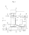
- FIG. 1 shows a schematic view of an exposure apparatus 10 of the embodiment.
- Exposure apparatus 10 is a scanning exposure apparatus by the step-and-scan method, or the so-called scanning stepper (also called a scanner) that transfers a circuit pattern formed on a reticle R serving as a mask onto each of a plurality of shot areas on a wafer W1 (or W2) serving as a photosensitive object, via a projection optical system PL serving as an exposure optical system, while synchronously moving reticle R and wafer W1 (or W2) in an one-dimensional direction (in this case, a Y-axis direction, which is the lateral direction of the page surface in FIG. 1 ).
- a scanning stepper also called a scanner
- Exposure apparatus 10 is equipped with an illumination system 12 that illuminates a reticle R with an illumination light IL, a reticle stag RST on which reticle R is mounted, projection optical system PL that projects illumination light IL outgoing from reticle R onto wafer W1 (or W2), a stage unit 20 that includes two substrate stages on which wafers W1 and W2 are respectively mounted, that is, wafer stages WST1 and WST2, an alignment system ALG serving as a mark detection system, a main controller 50 that has overall control over the entire unit, and the like.
- Illumination system 12 includes a light source and an illumination optical system, and irradiates illumination light IL on a rectangular or an arc-shaped illumination area IAR set by a field stop (also called a masking blade or a reticle blind) disposed inside the system, and illuminates reticle R on which the circuit pattern is formed with uniform illuminance.
- a field stop also called a masking blade or a reticle blind
- An illumination system similar to illumination system 12 is disclosed in, for example, Kokai (Japanese Unexamined Patent Application Publication) No. 6-349701 , and the corresponding U.S. Patent No. 5,534,970 , and the like.
- illumination light IL far ultraviolet light such as a KrF excimer laser beam (wavelength 248 nm) or an ArF excimer laser beam (wavelength 193 nm), or vacuum ultraviolet light such as an F 2 laser beam (wavelength 157 nm), or the like is used. Also, it is possible to use on emission line (such as a g-line or an i-line) in an ultraviolet region emitted from an ultra high-pressure mercury lamp as illumination light IL. As long as the national laws in designated states (or elected states), to which this international application is applied, permit, the above disclosures of the publication and the U.S. Patent are incorporated herein by reference.
- Reticle stage RST On reticle stage RST, for example, reticle R is fixed by vacuum chucking, electrostatic suction, or the like.
- Reticle stage RST is finely drivable in an X-axis direction, a Y-axis direction, and a ⁇ z direction (rotation direction around a Z-axis) within an XY plane perpendicular to the optical axis of illumination system 12 (coincides with an optical axis AX of projection optical system PL that will be described later) by a reticle stage drive section 22.
- Reticle stage RST is also drivable in a predetermined scanning direction (the Y-axis direction) along the upper surface of a reticle stage base (not shown) at a designated scanning speed.
- Reticle stage drive section 22 is a mechanism that uses a linear motor or a voice coil motor as its drives source, however, in FIG. 1 , reticle stage drive section 22 is shown simply as a block for the sake of convenience.
- reticle stage RST it is a matter of course that a stage that has a rough/fine movement structure can be employed, which has a rough movement stage drivable one dimensionally in the Y-axis direction, and a fine movement stage that can finely drive reticle R in at least directions of three degrees of freedom (the X-axis direction, the Y-axis direction, and the ⁇ z direction) with respect to the rough movement stage.
- the position (including the ⁇ z rotation) of reticle stage RST within the XY plane is constantly detected by a reticle laser interferometer (hereinafter referred to as 'reticle interferometer') 16 via a reflection surface formed (or arranged) on the edge section of reticle stage RST at a resolution of, for example, around 0.5 to 1 nm.
- the position information (including rotation information such as the ⁇ z rotation (yawing amount)) of reticle stage RST from reticle interferometer 16 is supplied to main controller 50.
- Main controller 50 controls the drive of reticle stage RST via reticle stage drive section 22, based on the position information of reticle stage RST.
- projection optical system PL As projection optical system PL, a both-side telecentric reduction system on the object surface side (reticle side) and the image plane side (wafer side) whose projection magnification is 1/4 (or 1/5) is used. Therefore, when illumination light (pulsed ultraviolet light) IL is irradiated on reticle R from illumination system 12, the imaging beams from the circuit pattern area formed on reticle R illuminated with the pulsed ultraviolet light enters projection optical system PL, and the image (a partially inverted image) of the circuit pattern within the irradiation area (illumination area IAR previously described) of illumination light IL is formed in the center of a field on the image plane side of projection optical system PL, limited in a narrow slit shape (or a rectangular shape (polygon)) extending in the X-axis direction, each time the purse irradiation of the pulsed ultraviolet light is performed.
- the partially inverted image of the circuit pattern projected is reduced and transferred onto a resist layer on the surface of a shot area among a plurality of shot areas on wafer M1 (or M2), which is disposed on the image-forming plane of projection optical system PL.
- a refracting system consisting of only a dioptric system (lens elements) is mainly used.
- a so-called catadioptric system which is a combination of dioptric elements and catoptric elements (such as a concave mirror or a beam splitter), or a reflection system consisting of only reflection optical elements, is mainly used, such as the ones disclosed in, for example, Kokai (Japanese Unexamined Patent Application Publication) No. 3-282527 , and the corresponding U.S. Patent No.
- Stage unit 20 is disposed below projection optical system PL in FIG. 1 .
- Stage unit 20 is equipped with wafer stages WST1 and MST2 that hold wafers M1 and W2, a drive mechanism that drives wafer stages MST1 and WST2, and the like.
- moving unit MUT1 is configured including frame 23, which has a rectangular frame shape in a planar view (when viewed from above), a stator unit 27, which includes a group of stators installed between one side wall and the other side wall off frame 23 in the X-axis direction whose longitudinal direction is in the X-axis direction, and wafer stage WST1, which engages with the group of stators constituting stator unit 27 and can be relatively moved.
- the other moving unit, moving unit MUT2 is configured including frame 123, which has a rectangular frame shape in a planar view (when viewed from above), a stator unit 127, which includes a group of stators installed between one side wall and the other side wall of frame 123 in the X-axis direction whose longitudinal direction is in the X-axis direction, and wafer stage WST2, which engages with the group of stators constituting stator unit 127 and can be relatively moved.
- As frames 23 and 123 a carbon monocoque frame, which is lightweight, is used.
- Y movers 33A and 33B are arranged, respectively.
- Y movers 133A and 133B are arranged, respectively, as is shown in FIG. 2 .
- one of the Y movers, Y mover 33A arranged in frame 23 is a magnetic unit that has a mover main body 39 being roughly shaped in the letter H in an XZ section, and of two sets of opposing surfaces in the X-axis direction that are vertically arranged in mover main body 39, the magnetic unit has a plurality of field magnets 93 that are each disposed along the Y-axis direction at a predetermined distance on the upper opposing surfaces in the X-axis direction, and a plurality of field magnets 95 that are each disposed along the Y-axis direction at a predetermined distance on the lower opposing surfaces.
- the adjacent field magnets in the Y-axis direction and the opposing field magnets in the X-axis direction each have a reversed polarity in the plurality of field magnets 93 and 95. Therefore, in the spaces vertically arranged inside mover main body 39, an alternating magnetic field (the direction of the magnetic flux is in the +X direction or the -X direction) is formed in the Y-axis direction, respectively.
- a gas hydrostatic bearing 41 is fixed on the +X side surface of mover main body 39 at substantially the center in the Z-axis direction.
- gas hydrostatic bearing 41 an outlet of the pressurized gas is formed on its lower surface (the -Z side surface).
- a magnetic unit substantially the same as Y mover 33A is used as the other Y mover, Y mover 33B, arranged in frame 23, however, a gas hydrostatic bearing 141, which is arranged on the -X side surface, is different from gas hydrostatic bearing 41 arranged in Y mover 33A. More specifically, gas hydrostatic bearing 141 has a gas outlet not only or the -Z surface side (the lower surface) but also on the -X surface side (the side surface).
- One of the Y movers, Y mover 133A, arranged in frame 123 is constituted in the same manner as Y mover 33A previously described, and the other Y mover, Y mover 133B is also constituted in the same manner as Y mover 33B previously described.
- the drive system is equipped with a pair of stator units 35A and 35B that engages with Y movers 33A and 33B, and Y movers 133A and 133B, and a guide mechanism 51 mainly composed of a plurality of members disposed outside stator units 35A and 35B.
- stator unit 35A is disposed on a floor surface F in the Y-axis direction at a predetermined distance.
- the stator unit has a pair of support columns 43A and 43B extending in the vertical direction, and two Y stators 45A and 45B whose longitudinal direction is the Y-axis direction, installed between support columns 43A and 43B and disposed vertically at a predetermined distance.
- Y stators 45A and 45B are armature units each having a housing whose XZ section is a narrow rectangle in the Z-axis direction, and a plurality of armature coils (not shown) disposed inside the housing along the Y-axis direction at a predetermined distance.
- Y stator 45A on the upper side has a shape that can engage with the spaces on the upper side of Y movers 33A and 133A (that is, the spaces where field magnets 93 are arranged), whereas Y stator 45B on the lower side has a shape that can engage with the spaces on the lower side of Y movers 33A and 133A (that is, the spaces where field magnets 95 are arranged).
- Y mover 33A does not actually engage with Y stator 45B.
- stator unit 35B is disposed on a floor surface F in the Y-axis direction at a predetermined distance.
- the stator unit has a pair of support columns 143A and 143B extending in the vertical direction, and two Y stators 145A and 145B whose longitudinal direction is the Y-axis direction, installed between support columns 143A and 143B and disposed vertically at a predetermined distance.
- Y stator 145A on the upper side has a shape that can engage with the spaces on the upper side of Y movers 33B and 133B
- Y stator 145B on the lower side has a shape that can engage with the spaces on the lower side of Y movers 33B and 133B.
- Y mover 33B does not actually engage with Y stator 145B.
- moving unit MUT1 is on a plane arranged at the height shown in FIG. 3 (the first surface described earlier), and Y mover 33A is engaged with Y stator 45A and Y mover 33B is engaged with Y stator 145A.
- reaction force of the Lorentz force generated by the electromagnetic interaction between the current that flows in the armature coil that constitutes Y stator 45A and the alternating magnetic field generated by field magnets (field magnets on the upper side) 93 installed in Y mover 33A acts on Y mover 33A as a drive force in the Y-axis direction
- reaction force of the Lorentz force generated by the electromagnetic interaction between the current that flows in the armature coil that constitutes Y stator 145A and the alternating magnetic field generated by field magnets 93 installed in Y mover 33B also acts on Y mover 33B as a drive force in the Y-axis direction.
- Y mover 33A and Y stator 45A constitute a moving magnet type Y-axis linear motor
- Y mover 33B and Y stator 145A also constitute a moving magnet type Y-axis linear motor
- moving unit MUT1 is reciprocally driven in the Y-axis direction in predetermined strokes.
- the pair of Y-axis linear motors will each be referred to as Y-axis linear motor 33A and Y-axis linear motor 33B, respectively, using the same reference numerals as the respective movers.
- Y mover 133A is engaged with Y stator 45B on the lower side and Y mover 133B is engaged with Y stator 145B on the lower side.
- Y mover 133A and Y stator 45B constitute a moving magnet type Y-axis linear motor by the electro-magnetic drive method
- Y mover 133B and Y stator 145B also constitute a moving magnet type Y-axis linear motor by the electro-magnetic drive method
- Y-axis linear motor 45B Y-axis linear motor 45B
- Y-axis linear motor 145B Y-axis linear motor 145B
- moving unit MUT2 is driven upward by a first vertical movement mechanism and a second vertical movement mechanism, which will be described later, and is also made to be positioned at the same height position as moving unit MUT1 in FIGS. 2 and 3 .
- Y mover 133A is engaged with Y stator 45A on the upper side
- Y mover 133B is engaged with Y stator 145A on the upper side.
- Y mover 133A and Y stator 45A constitute a moving magnet type Y-axis linear motor by the electro-magnetic drive method
- Y mover 133B and Y stator 145A also constitute a moving magnet type Y-axis linear motor by the electro-magnetic drive method
- moving unit MUT2 set at the same height as MUT1 shown in FIGS. 2 and 3 is reciprocally driven on the first surface previously described in the Y-axis direction in predetermined strokes.
- the pair of Y-axis linear motors will each be referred to as Y-axis linear motor 45A and Y-axis linear motor 145A, respectively, using the same reference numerals as the respective stators.
- guide mechanism 51 is equipped with a first guide section 52A and a second guide section 52B, disposed at a predetermined distance in the X-axis direction, and a connecting plate 61 for connecting a part of the guide sections.
- the first guide section 52A is configured of three sections; a fixed guide 53A, arranged on floor surface F facing Y stator 45B constituting stator unit 35A at substantially the center of the longitudinal direction, an elevator unit EU1 arranged on one side (the +Y side) of fixed guide 53A in the Y-axis direction, and an elevator unit EU2 arranged on the other side (the -Y side) of fixed guide 53A in the Y-axis direction.
- fixed guide 53A is composed of a generally cuboid member whose longitudinal direction is in the Y-axis direction and has a recessed groove with a rough U-shaped section formed on the surface on the -X side, and the upper end surface of the cuboid member is a first guide surface 153a shown in FIG. 5 . Further, of a pair of opposing surfaces of the recessed groove formed at the center in the height direction on the -X side of fixed guide 53A, the surface on the lower side is a second guide surface 153b shown in FIGS. 3 and 5 .
- the pressurized gas from gas hydrostatic bearing 41 arranged in Y mover 33A or Y mover 133A blows on the first guide surface 153a, and by the static pressure of the pressurized gas, moving unit MUT1 or moving unit MUT2 is supported by levitation in a non-contact manner, via a clearance of several ⁇ m between gas hydrostatic bearing 41 and guide surface 153a. Further, the pressurized gas from gas hydrostatic bearing 41 arranged in moving unit MUT2, which is at the height position shown in FIG.
- moving unit MUT2 blows on the second guide surface 153b, and by the static pressure of the pressurized gas, moving unit MUT2 is supported by levitation in a non-contact manner, via a clearance of several ⁇ m between gas hydrostatic bearing 41 and guide surface 153b.
- elevator unit EU1 has a fixed block 65A composed of a cuboid member, which is disposed diagonally to fixed guide 53A at a position both on the +Y side and the +X side of fixed guide 53A, and a square-prism shaped vertical movement guide 55A whose longitudinal direction is the Y-axis direction, disposed on the -X side of fixed block 65A and has a guide groove 155b in the vertical direction as is shown in FIG. 3 on the surface on the +X side.
- movers are embedded inside guide groove 155b of vertical movement guide 55A, and facing the movers on the surface on the -X side of fixed block 65A, a stator 66A, which configures a shaft motor (or a linear motor) along with the mover, is arranged (refer to FIG. 3 ).
- the shaft motor drives vertical movement guide 55A in the vertical direction (the Z-axis direction) with respect to fixed block 65A.
- the shaft motor will be referred to as shaft motor 66A, using the same reference numerals as the stator.
- the upper surface of vertical movement guide 55A is a guide surface 155a, and the pressurized gas from gas hydrostatic bearing 41 arranged in Y mover 133A blows on guide surface 155a.
- Vertical movement guide 55A is driven by shaft motor 66A, between a lower moving limit position shown in FIG. 5 where guide surface 155a becomes in plane with the second guide surface 153b and an upper moving limit position shown in FIG. 6 where guide surface 155a becomes in plane with the first guide surface 153a.
- elevator unit EU2 has a fixed block 67A composed of a cuboid member, which is disposed diagonally to fixed guide 53A at a position both on the -Y side and the +X side of fixed guide 53A, and a square-prism shaped vertical movement guide 57A whose longitudinal direction is the Y-axis direction, disposed on the -X side of fixed block 67A and has a guide groove 157b in the vertical direction as is shown in FIG. 3 on the surface on the +X side.
- movers are embedded inside guide groove 157b of vertical movement guide 57A, and facing the movers on the surface on the -X side of fixed block 67A, a stator 68A, which configures a shaft motor (or a linear motor) along with the mover, is arranged (refer to FIG. 3 ).
- the shaft motor drives vertical movement guide 57A in the vertical direction (the Z-axis direction) with respect to fixed block 67A.
- the shaft motor will be referred to as shaft motor 68A, using the same reference numerals as the stator.
- the upper surface of vertical movement guide 57A is a guide surface 157a, and the pressurized gas from gas hydrostatic bearing 41 arranged in Y mover 133A blows on guide surface 157a.
- Vertical movement guide 57A is driven by shaft motor 68A, between a lower moving limit position shown in FIG. 5 where guide surface 157a becomes in plane with the second guide surface 153b and an upper moving limit position shown in FIG. 6 where guide surface 157a becomes in plane with the first guide surface 153a.
- the second guide section 52B is configured of three sections; a fixed guide 53B, arranged on floor surface F facing Y stator 145B constituting stator unit 35B at substantially the center of the longitudinal direction, an elevator unit EU3 arranged on one side (the +Y side) of fixed guide 53B in the Y-axis direction, and an elevator unit EU4 arranged on the other side (the -Y side) of fixed guide 53B in the Y-axis direction.
- fixed guide 53B is composed of a generally cuboid member whose longitudinal direction is in the Y-axis direction, and on the upper end section on the +X side surface, a step section with an L-shaped section is formed, and below the step section, a recessed groove with a rough U-shaped section is formed.
- the upper surface of the step section with the L-shaped section of fixed guide 53B is a guide surface 253a and the side surface is a guide surface 253b.
- the surface on the lower side is a guide surface 253c shown in FIG.
- Fixed guide 53B is disposed on the floor surface in a state facing fixed guide 53A previously described, and is connected to fixed guide 53A via connecting plate 61.
- elevator unit EU3 has a fixed block 65B composed of a cuboid member, which is disposed diagonally to fixed guide 53B at a position both on the +Y side and the -X side of fixed guide 53B, and a square-prism shaped vertical movement guide 55B whose longitudinal direction is the Y-axis direction, disposed on the +X side of fixed block 65B.
- a guide groove of the vertical direction that has movers (not shown) embedded inside is formed on the surface of vertical movement guide 55B on the +X side, and facing the groove, a stator 66B, which configures a shaft motor (or a linear motor) along with the mover, is arranged.
- the shaft motor drives vertical movement guide 55B in the vertical direction (the Z-axis direction) with respect to fixed block 65B.
- the shaft motor will be referred to as shaft motor 66B, using the same reference numerals as the stator.
- guide surfaces 255a and 255b are formed that become flush with guide surfaces 253c and 253d described earlier, respectively, in a state shown in FIG. 5 .
- Vertical movement guide 55B is driven by shaft motor 66B, between the lower moving limit position shown in FIG. 5 where guide surface 255a becomes in plane with guide surface 253c and the upper moving limit position shown in FIG. 6 where guide surface 255a becomes in plane with guide surface 253a.
- guide surfaces 257a and 257b are formed that become flush with guide surfaces 253c and 253d described earlier, respectively, in a state shown in FIG. 5 .
- guide surface 257b also functions as a yaw guide to moving unit MUT2.
- Vertical movement guide 57B is driven by shaft motor 68B, between the lower moving limit position shown in FIG. 5 where guide surface 257a becomes in plane with guide surface 253c and the upper moving limit position shown in FIG. 6 where guide surface 257a becomes in plane with guide surface 253a.
- moving unit MUT2 can be reciprocally moved along the Y-axis direction from the moving limit position on the +Y side of vertical movement guides 55A and 57A to the moving limit position on the -Y side of vertical movement guides 55B and 57B.
- the height of guide surface 155a of vertical movement guide 55A, guide surface 157a of vertical movement guide 57A, and the first guide surface 153a of fixed guide 53A coincide with one another, while the height of guide surface 255a of vertical movement guide 55B, guide surface 257a of vertical movement guide 57B, and guide surface 253a of fixed guide 53B also coincide with one another.
- Stator 46A whose longitudinal direction is the X-axis direction, has a housing that has both one end and the other end in the longitudinal direction fixed to frame 23 so that the housing is substantially parallel to the XZ plane, and a plurality of armature coils (not shown) disposed at a predetermined distance in the X-axis direction inside the housing.
- stator 46D has a housing whose longitudinal direction is in the X-axis direction and is arranged below stator 46B in a substantially parallel manner, and one or a plurality of armature coils disposed inside the housing, such as for example, a pair of a rectangular-shaped armature coils extending narrowly in the X-axis direction, disposed in the Y-axis direction at a predetermined distance.
- stator 46C is configured similarly to stator 46B, and is disposed substantially parallel to stator 46D below stator 46D. In this case, stator 46B and stator 46C are disposed vertically symmetric, with stator 46D as the center.
- Stator 46E has a housing whose longitudinal direction is in the X-axis direction and is arranged a predetermined distance away on the -Y side of stator 46A in a substantially parallel manner, and one or a plurality of armature coils disposed inside the housing, such as for example, a pair of a rectangular-shaped armature coils extending narrowly in the X-axis direction, disposed in the Z-axis direction at a predetermined distance.
- stator 46F has a housing whose longitudinal direction is in the X-axis direction and is arranged on the +Y side of stators 46B to 46D so that the housing is parallel to the XZ plane, and one or a plurality of armature coils disposed inside the housing, such as for example, a pair of a rectangular-shaped armature coils extending narrowly in the X-axis direction, disposed in the Z-axis direction at a predetermined distance.
- Support plate 29 is composed of a plate-shaped member whose one end and the other end in the longitudinal direction is fixed to frame 23, and is arranged so that the plate-shaped member is substantially parallel to the XY plane and extending in the X-axis direction.
- Support plate 29 is a plate-like member with high rigidity, and as it will be described later in the description, the plate is used to support the weight of wafer stage WST1 (maintain the Z position of wafer stage WST1).
- the other staler unit 127 is configured in a similar manner as stator unit 27 described above.
- mover 44A is fixed to wafer stage main body 31 on the side surface on the -Y side, and mover 44A has a yoke 52 that has a rectangular YZ section and a tube-like shape in general, and a plurality of field magnets 54 disposed inside yoke 52 on the lateral opposing surfaces at a predetermined distance along the X-axis direction.
- the adjacent field magnets 54 in the X-axis direction and the opposing field magnets 54 in the Z-axis direction each have a reversed polarity. Therefore, in the space inside yoke 52, an alternating magnetic field (the direction of the magnetic field is in the +Y direction and the -Y direction) is formed in the X-axis direction.
- stator 46A described earlier is inserted into the inner space of yoke 52, and by the Lorentz force generated by the electromagnetic interaction between the current that flows in the plurality of the armature coils that constitute stator 46A and the alternating magnetic field in the inner space of yoke 52 of mover 44A, a drive force in the X-axis direction acts on Y mover 44A, and mover 44A is driven along stator 46A in the X-axis direction.
- stator 46A and mover 44A constitute an X-axis linear motor LX 1 composed of a moving magnet type Y-axis linear motor (refer to FIG. 7A ).
- Movers 44B, 44D, and 44C correspond to stators 46B, 46D, and 46C previously described, respectively, and according to the arrangement of the stators, the movers are fixed to the side surface of wafer stage main body 31 on the +Y side, in a state vertically stacked in the order of movers 44B, 44D,and 44C.
- stator 46B and mover 44B constitute an X-axis linear motor LX 2 composed of a moving magnet type linear motor (refer to FIG. 7A ).
- stator 46C and mover 44C constitute an X-axis linear motor LX 3 composed of a moving magnet type linear motor (refer to FIG. 7A ).
- wafer stage WST1 can be driven in the X-axis direction (a substantially centroid drive) with respect to the group of stators in stator unit 27 and support plate 29.
- wafer stage WST1 can be finely driven in the rotation direction around the Y-axis (the rolling direction), and also by making the resultant force of the drive forces generated by X-axis linear motors LX 2 and LX 3 and the drive force generated by X-axis linear motor LX 2 different, wafer stage MST1 can be finely driven in the rotation direction around the Z-axis (the yawing direction).
- stator 46D is inserted between permanent magnets 58A and 58B, and half the section substantially on the inner side of each of the pair of armature coils that constitute stator 46D is included in the magnetic field between permanent magnets 58A and 58B described above.
- stator 46E is inserted between permanent magnets 62A and 62B, and half the section substantially on the inner side of each of the pair of armature coils that constitute stator 46E is included in the magnetic field between permanent magnets 62A and 62B described above.
- mover 44E and stator 46E constitute a first Z-axis fine movement motor VZ 1 that finely drives wafer stage WST1 in the Z-axis direction (refer to FIG. 7A ).
- mover 44F is arranged on the +Y side of movers 44B, 44D, and 44C, and the configuration is similar to mover 44E.
- mover 44F and stator 46F constitute a second Z-axis fine movement motor VZ 2 that finely drives wafer stage WST1 (and mover 44F) in the Z-axis direction with respect to stator 46F (refer to FIG. 7A ).
- wafer stage WST1 can be finely driven in the Z-axis direction, whereas by making each Z-axis fine movement motor generate a different drive force, wafer stage WST1 can be finely driven in a rotation direction around the X-axis (the pitching direction).
- Y-axis fine movement motor VY, X-axis linear motors LX 1 to LX 3 , and the first Z-axis fine movement motor VZ 1 and the second Z-axis fine movement motor VZ 2 constitute a six degrees of freedom drive mechanism, which drives wafer stage WST1 in directions of six degrees of freedom with respect to stator unit 27.
- a through hole 31a is formed along the X-axis direction as is shown in FIG. 7B , and in the state shown in FIG. 2 where wafer stage WST1 is engaged with the group of stators in stator unit 27 and support plate 29, support plate 29 is in a state inserted into through hole 31a.
- a deadweight canceller (not shown) is arranged inside through hole 31a.
- the deadweight canceller has a cylinder section and a piston section, and is set at a positive pressure by the gas supplied inside the cylinder section. And, the positive pressure inside the cylinder section supports the entire wafer stage WST1 in a state relatively movable with respect to support plate 29.
- Support plate 29 and the deadweight canceller do not necessarily have to be arranged, and in the case support plate 29 and the deadweight canceller are not arranged, the deadweight of wafer stage WST1 can be supported by making the first Z-axis fine movement motor VZ 1 and the second Z-axis fine movement motor VZ 2 generate a force in the Z-axis direction that balances with the deadweight of wafer stage WST1.
- a through hole is formed corresponding to the support plate as in wafer stage main body 31 on the wafer stage WST1 side, and in the state where wafer stage WST2 is engaged with the group of stators in stator unit 127 and the support plate, the entire wafer stage WST1 is supported in a state relatively movable with respect to the support plate by the deadweight canceller arranged in the through hole section.
- an X movable mirror MX1 extending in the Y-axis direction is arranged on one end (the end section on the +X side) in the X-axis direction
- a Y movable mirror MY1a extending in the X-axis direction is arranged on one end (the end section on the +Y side) in the Y-axis direction
- a Y movable mirror MY1b extending in the X-axis direction is arranged on the other end (the end section on the -Y side) in the Y-axis direction.
- wafer M1 is fixed by electrostatic suction or by vacuum chucking via a wafer holder (not shown).
- a wafer holder not shown.
- FIG. 1 only movably mirrors MY1a and MY1b for measuring the position in the Y-axis direction are shown as the movable mirrors on the wafer stage WST1 side.
- an X movable mirror MX2 extending in the Y-axis direction is arranged on one end (the end section on the +X side) in the X-axis direction
- a Y movable mirror MY2a extending in the X-axis direction is arranged on one end (the end section on the +Y side) in the Y-axis direction
- a Y movable mirror MY2b extending in the X-axis direction is arranged on the other end (the end section on the -Y side) in the Y-axis direction.
- interferometer beams (measurement beams) from interferometers of each measurement beam constituting an interferometer system, which will be described later, are projected, and the lights reflected off the reflection surfaces are received by the interferometers, which measure the displacement of each of the reflection surfaces of the movable mirrors from a reference position, and by this operation, the two-dimensional position of wafer stage WST2 is measured.
- wafer W2 is fixed by electrostatic suction or by vacuum chucking via a wafer holder (not shown). In FIG. 1 , however, only movably mirrors MY2a and MY2b for measuring the position in the Y-axis direction are shown as the movable mirrors on the wafer stage WST2 side.
- the magnitude and the direction of the current supplied to each of the armature coils that make up each of the motors described above constituting stage unit 20 is controlled by main controller 50 in FIG. 1 . Accordingly, the magnitude and direction of the drive force that each motor generates is arbitrarily controlled.
- an interferometer beam (a measurement beam) is irradiated from a Y interferometer 116, in the direction parallel to the Y-axis passing through the optical axis of projection optical system PL from Y interferometer 116.
- an interferometer beam (a measurement beam) is irradiated from a Y interferometer 118, in the direction parallel to the Y-axis passing through the detection center (the center of the index mark) of alignment system ALG from interferometer 118.
- Y-axis interferometers 116 and 118 by receiving the lights reflected off movable mirrors MY1b and MY2a, respectively, the relative displacement from the reference position of each reflection surface is measured, and the position of wafer stage WST1 and WST2 in the Y-axis direction is measured.
- Y-axis interferometers 116 and 118 are both multi-axis interferometers, and other than measuring the position information of wafer stage WST1 and MST2 in the Y-axis direction, Y-axis interferometers 116 and 118 can also measure pitching (rotation around the X-axis ( ⁇ x rotation)) and yawing (rotation in the ⁇ z direction). The output values of each measurement axis can be measured independently.
- an interferometer beam (a measurement beam), which passes through the optical axis of projection optical system PL and perpendicularly crosses the interferometer beam from Y interferometer 116, is irradiated from an X interferometer (not shown).
- an interferometer beam (a measurement beam), which passes through the detection center (the center of the index mark) of alignment system ALG and perpendicularly crosses the interferometer beam from Y interferometer 118, is irradiated from an X interferometer (not shown).
- the X-axis interferometers are multi-axis interferometers, and other than measuring the position information of wafer stage WST1 and WST2 in the X-axis direction, X-axis interferometers can also measure rolling (rotation around the Y-axis ( ⁇ y rotation)) and yawing (rotation in the ⁇ z direction). The output values of each measurement axis can be measured independently.
- a total of four interferometers the two X-axis interferometers and Y-axis interferometers 116 and 118, constitute a wafer interferometer system that controls the XY two-dimensional coordinate position of wafer stages MST1 and WST2.
- the measurement values of each of the interferometers that make up the system are sent to main controller 50.
- the X-axis interferometer that emits the interferometer beam passing through the detection center (the center of the index mark) of alignment system ALG and perpendicularly crosses the interferometer beam from Y interferometer 118 will be referred to as an alignment X-axis interferometer
- the X-axis interferometer that emits the interferometer beam which passing through the optical axis of projection optical system PL and perpendicularly crosses the interferometer beam from Y interferometer 116 will be referred to as an exposure X-axis interferometer.
- Main controller 50 controls the position of wafer stages WST1 and WST2 within the XY plane with high precision, without any of the so-called Abbe errors, based on the measurement values of exposure X-axis interferometer and Y interferometer 116 on exposure, which will be described later, whereas, on wafer alignment, which will also be described later, main controller 50 controls the position of wafer stages WST1 and WST2 within the XY plane with high precision, without any of the so-called Abbe errors, based on the measurement values of alignment X-axis interferometer and Y interferometer 118.
- moving units MUT1 and MUT2 do not constantly maintain the position relation shown in FIGS. 1 , 2 , and the like, and as it will be described later, wafer stages WST1 and WST2 will be interchanged, and the case may occur where the interferometer beams will not irradiate the movable mirrors on wafer stage MST2.
- linear encoders (not shown) that can constantly measure the position information of moving unit MUT2 in the Y-axis direction are arranged at predetermined positions.
- a case where the interferometer beams from the X-axis interferometers will not irradiate the movable mirrors on wafer stages WST1 and WST2 when wafer stages WST1 and WST2 are moving in the Y-axis direction may occur.
- main controller 50 resets (or presets) the measurement values of the interferometer that could not perform measurement.
- FIG. 8A shows the state where in parallel with the exposure operation of wafer W1 on wafer stage WST1 via projection optical system PL under the control of main controller 50, wafer alignment operation using alignment system ALG is being performed on wafer M2 on wafer stage WST2 ( FIG. 8A corresponds to the state shown in FIG. 1 )
- a wafer loader Prior to the state in FIG. 8A , when wafer stage WST2 (and moving unit MUT2) is at a predetermined loading position (in the vicinity of the alignment position), a wafer loader (not shown) performs unloading of the wafer mounted on wafer stage WST2 that has been exposed and loading of a new wafer W2 (that is, wafer exchange) onto wafer stage WST2.
- main controller 50 detects the position information of alignment marks (sample marks) arranged in a specific plurality of shot areas (sample shot areas) on wafer W2, while controlling the position of wafer stage WST2 within the XY plane based on the measurement values of Y interferometer 118 and alignment X-axis interferometer described above.
- main controller 50 performs wafer alignment by the EGA (Enhanced Global Alignment) method in order to obtain the arrangement coordinates of all the shot areas on wafer W2 by statistical calculation using the least square method, as is disclosed in, for example, Kokai (Japanese Unexamined Patent Application Publication) No. 61-44429 , and the corresponding U.S. Patent No. 4,780,617 , and the like.
- EGA Enhanced Global Alignment
- main controller 50 detects the position information of a first fiducial mark on the fiducial mark plate (not shown) on wafer stage WST2. Then, main controller 50 converts the arrangement coordinates of all the shot areas on wafer W2 obtained in advance into position coordinates whose origin is set to the position of the first fiducial mark.
- wafer exchange and wafer alignment is executed on the wafer stage WST2 side.
- an exposure operation by the step-and-scan method is performed under the control of main controller 50 where a stepping operation between shots in which wafer stage WST1 is moved to the acceleration starting position for exposure of each shot area on wafer W1 mounted on wafer stage WST1 based on the wafer alignment results that has been performed earlier, and a scanning exposure operation where the pattern formed on reticle R is transferred onto the shot areas subject to exposure on wafer W1 via projection optical system PL by relatively scanning reticle R (reticle stage RST) and water W1 (wafer stage WST1) in the Y-axis direction are repeated.
- main controller 50 Prior to starting the exposure operation by the step-and-scan method referred to above, main controller 50 measures a pair of second fiducial marks on the fiducial mark plate (not shown) on wafer stage WST1 and a pair of reticle alignment marks on reticle R using a reticle alignment system (not shown), while controlling the position of wafer stage WST1 based on the measurement values of Y-axis interferometer 116 and exposure X-axis interferometer.
- main controller 50 moves wafer stage WST1 to the acceleration starting position for exposing each of the shot areas on wafer W1.
- main controller 50 drives moving unit MUT1 (wafer stage WST1) in the Y-axis direction with long strokes using Y-axis linear motors 33A and 33B previously described, and also finely drives wafer stage WST1 in the X, Y, Z, ⁇ x, ⁇ y, and ⁇ z directions via the six degrees of freedom drive mechanism previously described that constitutes moving unit MUT1. Further, when main controller 50 drives wafer stage WST1 in the X-axis direction with long strokes, main controller 50 uses the three X-axis linear motors LX 1 to LX 3 that make up the six degrees of freedom drive mechanism of moving unit MUT1.
- main controller 50 performs the interchange of the wafer stage in parallel, and moves moving unit MUT2 containing wafer stage WST2 to the -Y side of moving unit MUT1 by masking moving unit MUT2 pass under moving unit MUT1.
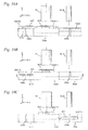
- main controller 50 drives vertical movement guides 55A and 55B downward via shaft motors 66A and 66B, from the upper end moving position shown in FIG. 8A to the lower end moving position shown in FIG. 8B . And, by the downward drive of vertical movement guides 55A and 55B, moving unit MUT2 is driven downward, and the pair of Y movers 133A and 133B installed in moving unit MUT2 becomes engaged with Y stators 45B and 145B, respectively.
- main controller 50 drives Y-axis linear motors 45B and 145B while monitoring the measurement values of the encoder previously described, and drives moving unit MUT2 from the position shown in FIG. 8B on vertical movement guides 55A and 55B to the position shown in FIG. 9A on vertical movement guides 57A and 57B, via the position shown in FIG. 8C on fixed stators 53A and 53B (the position under moving unit MUT1).
- main controller 50 drives vertical movement guides 57A and 57B further upward to the upper end moving position shown in FIG. 9B via shaft motors 68A and 68B.
- wafer stage WST2 rises to the height position shown in FIG. 9B , and during this movement, the interferometer beams from interferometer 116 moves away from movable mirror MY1b on wafer stage WST1 and at the same time begins to irradiate movable mirror MY2b on wafer stage WST2.
- main controller 50 switches the interferometer that measures the position of wafer stage WST2 in the Y-axis direction to Y-axis interferometer 118 whose interferometer beams are irradiating movable mirror MY1a at this point. Further, main controller 50 also switches the measurement unit used for measuring the Y-axis position of wafer stage WST2 (moving unit MUT2) from the encoder to Y-axis interferometer 116.
- vertical movement guides 55A and 55B are driven to the upper end moving position by shaft motors 66A and 66B, as is shown in FIG. 9B .
- main controller 50 drives Y-axis linear motor 45A and 145A, and Y-axis liner motors 33A and 33B, respectively, and moves both wafer stage WST2 (moving unit MUT2) and wafer stage WST1 (moving unit MUT1) in the +Y direction as is shown in FIG. 9C .
- main controller 50 moves wafer stage WST2 until the fiducial mark plate is positioned under projection optical system PL, and moves wafer stage WST1 to the wafer exchange position.
- main controller 50 measures the pair of the second fiducial marks on fiducial mark plate on wafer stage WST2 and the pair of reticle alignment marks on reticle R using the reticle alignment system previously described, and after the measurement, the exposure operation of each shot area on wafer W2 by the step-and-scan method begins (refer to FIG. 9C ), based on the measurement results and the results or wafer alignment referred to earlier.
- wafer W1 is unloaded via a wafer carrier unit (not shown), and the next wafer (in this case, the wafer is wafer W3) is loaded via the wafer carrier unit.
- main controller 50 performs wafer alignment on wafer W3 on wafer stage WST1.
- main controller 50 moves wafer stage WST2 (moving unit MUT2) and wafer stage WST1 (moving unit MUT1) in parallel, in the -Y direction (refer to FIG. 10A ).
- main controller 50 drives vertical movement guides 57A and 57B downward, as is shown in FIG. 10B . And by this downward drive, the interferometer beams from interferometer 116 that has been irradiating movable mirror MY2b on wafer stage WST2 moves away from movable mirror MY2b, and at begins to irradiate movable mirror MY1b on wafer stage WST1. Therefore, main controller 50 switches the interferometer that measures the Y position of wafer stage WST1 to Y-axis interferometer 116.
- the interferometer beams from the exposure X-axis interferometer irradiate movable mirror MX1 on wafer stage WST1, and the X position of wafer stage MST1 is measured by the exposure X-axis interferometer.
- the position of wafer stage WST1 within the XY plane is measured by the exposure X-axis interferometer and Y-axis interferometer 116.
- main controller 50 Almost simultaneously with the downward drive of driving vertical movement guides 57A and 57B, main controller 50 also drives vertical movement guides 55A and 55B downward from the upper end moving position in FIG. 10A to the lower end position shown in FIG. 10B .
- main controller 50 moves moving unit MUT2 (wafer stage WST2) in the +Y direction using Y-axis linear motors 45B and 145B, to the position shown in FIG. 10C passing through the position below moving unit MUT1 (wafer stage WST1). Furthermore, from the state shown in FIG. 10C , main controller 50 drives vertical movement guides 55A and 55B upward, which brings the guides back into the state shown in FIG. 8A . Also in this case, main controller 50 switches from the position measurement of wafer stage WST2 by the encoder to the position measurement by the interferometer.
- the drive system (33A, 33B, 133A, 133B, 35A, 35B, and 51) described earlier and main controller 50 configure an exchange unit.
- the elevator units EU1 and EU3 configure a first vertical movement mechanism
- the elevator units EU2 and EU4 configure a second vertical movement mechanism.
- the apparatus is equipped with an exchange unit (33A, 33B, 133A, 133B, 35A, 35B, 51, and 50) that switches both wafer stages WST1 and WST2 between the exposure operation of the wafer by projection optical system PL and the mark detection operation (wafer alignment operation) on the wafer by alignment system ALG in a procedure where of the two wafer stages WST1 and WST2, one of the wafer stages, wafer stage WST2 (specific stage) is positioned temporarily below the remaining wafer stage, wafer stage WST1.
- an exchange unit 33A, 33B, 133A, 133B, 35A, 35B, 51, and 50
- the exchange unit makes it possible to perform a part of the interchange operation (exchange operation) of both wafer stages according to the procedure where the other stage, wafer stage WST2, which has completed the detection operation of the marks on the wafer by alignment system ALG in the vicinity of the second position (the position where alignment system ALG is disposed) is positioned temporarily below one of the stages, wafer stage WST1, in parallel with the exposure operation by projection optical system PL of the wafer on one of the stages, wafer stage WST1, positioned in the vicinity of the first position (the position where projection optical system PL is disposed).
- the time required for the interchange can be reduced when compared with the case where the interchange operation of both stages begin when the exposure operation of the wafer on one of the stages has been completed, which makes it possible to improve the throughput of the exposure processing step where exposure of the wafer on the two wafer stages is alternately performed.
- the interchange of the wafer stages can be achieved by simply moving each of the wafer stages along a path decided in advance, without performing the operation with uncertainty as in a mechanically grasping operation previously described. Therefore, the position alignment that was necessary when mechanically grasping operation was performed will not be required, and displacement of the wafer will not occur, so the exposure accuracy will not be reduced in particular. Further, since only one alignment system ALG will be required, the problems that occur due to having a plurality of alignment systems will also be resolved.
- wafer stages WST1 and WST2 are alternately moved with respect to the first position (predetermined position) below projection optical system PL by the exchange unit described above, only one of the wafer stages of the two wafer stages, wafer stage WST2, is moved so as to be temporarily positioned below the other wafer stage MST1. That is, by wafer stage WST1 moving within a predetermined plane (the first plane previously described) and only wafer stage WST2 moving vertically and within the first plane, wafer stages WST1 and WST2 can be alternately moved to the first position. Accordingly, the two wafer stages, WST1 and WST2, can be alternately moved to the first position, for example, without the wirings and the like connected to wafer stages WST1 and WST2 being entangled.
- a predetermined plane the first plane previously described
- the specific stage may be both wafer stage WST1 and wafer stage WST2.
- the exchange unit can perform the exchange (interchange) of wafer stage WST1 and wafer stage WST2 according to a procedure where the wafer stage holding the wafer on which wafer alignment has been completed, which is the specific stage, is temporarily kept waiting under the remaining wafer stage where the exposure of the wafer is performed, and the apparatus may employ a structure where wafer stages WST1 and WST2 are circulated.
- illumination light IL far ultraviolet light such as the KrF excimer laser beam, vacuum ultraviolet light such as the F 2 laser or the ArF excimer laser, or bright lines (such as the g-line or the i-line) in the ultraviolet region from an ultra high-pressure mercury lamp is used.
- far ultraviolet light such as the KrF excimer laser beam
- vacuum ultraviolet light such as the F 2 laser or the ArF excimer laser
- bright lines such as the g-line or the i-line
- the Ar 2 laser beam wavelength 126 nm
- illumination light IL is not limited to the laser beams emitted from the light sources described above, and a harmonic may also be used that is obtained by amplifying a single-wavelength laser beam in the infrared or visible range emitted by a DFB semiconductor laser or fiber laser, with a fiber amplifier doped with, for example, erbium (Er) (or both erbium and ytteribium (Yb)), and by converting the wavelength into ultraviolet light using a nonlinear optical crystal.
- Er erbium
- Yb ytteribium
- the present invention can also be applied to an exposure apparatus that uses an EUV light, an X-ray, or a charged particle beam such as an electron beam or an ion beam as illumination light IL.
- a charged particle beam optical system such as the electron optical system will constitute the exposure optical system.
- the present invention can also be applied to an immersion exposure apparatus that has a liquid filled in the space between projection optical system PL and the wafer whose details are disclosed in, for example, International Publication No. WO99/49504 or the like.
- the present invention is applied to a scanning exposure apparatus based on the step-and-scan method. It is a matter of course, however, that the present invention is not limited to this. More specifically, the present invention can also be suitably applied to a reduction projection exposure apparatus based on a step-and-repeat method.
- the exposure apparatus in the embodiment above can be made by incorporating the illumination optical system made up of a plurality of lenses and the projection optical system into the main body of the exposure apparatus, performing the optical adjustment operation, and also attaching the reticle stage and the wafer stages made up of multiple mechanical parts to the main body of the exposure apparatus, connecting the wiring and piping, and then, further performing total adjustment (such as electrical adjustment and operation check).
- the exposure apparatus is preferably built in a clean room where conditions such as the temperature and the degree of cleanliness are controlled.
- the present invention is not limited to the exposure apparatus for manufacturing semiconductors, and the present invention can also be applied to an exposure apparatus used for manufacturing liquid crystal displays that transfers a liquid crystal display device pattern onto a glass plate, an exposure apparatus used for manufacturing thin film magnetic heads that transfers a device pattern onto a ceramic wafer, and to an exposure apparatus used for imaging devices (such as CCDs), micromachines, organic ELs, DNA chips, and the like.
- the present invention can also be suitably applied to an exposure apparatus that transfers a circuit pattern onto a glass substrate or a silicon wafer not only when producing microdevices such as semiconductors, but also when producing a reticle or a mask used in exposure apparatus such as an optical exposure apparatus, an EUV exposure apparatus, an X-ray exposure apparatus, and an electron beam exposure apparatus.
- the exposure apparatus that uses DUV (deep (far) ultraviolet) light or VUV (vacuum ultraviolet) light, a transmittance type reticle is used, and as the reticle substrate, materials such as silica glass, fluorine-doped silica glass, fluorite, magnesium fluoride, or crystal are used.
- a transmittance type mask a stencil mask, a membrane mask
- the mask substrate silicon wafer or the like is used.
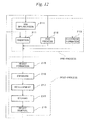
- FIG. 11 shows the flowchart of an example when manufacturing a device (a semiconductor chip such as an IC or an LSI, a liquid crystal panel, a CCD, a thin-film magnetic head, a micromachine, and the like).
- a device a semiconductor chip such as an IC or an LSI, a liquid crystal panel, a CCD, a thin-film magnetic head, a micromachine, and the like.
- step 201 design step
- function and performance design of device circuit design of semiconductor device, for example
- pattern design to realize the function is performed.
- step 202 mask manufacturing step
- a mask on which the designed circuit pattern is formed is manufactured.
- step 203 wafer manufacturing step
- a wafer is manufactured using materials such as silicon.
- step 204 wafer processing step
- step 205 device assembly step
- Step 205 includes processes such as the dicing process, the bonding process, and the packaging process (chip encapsulation), and the like when necessary.
- step 206 (inspection step), tests on operation, durability, and the like are performed on the devices made in step 205. After these steps, the devices are completed and shipped out.
- FIG. 12 is a flow chart showing a detailed example of step 204 described above.
- step 211 oxidation step
- step 212 CDV step
- an insulting film is formed on the wafer surface.
- step 213 electrode formation step
- step 214 ion implantation step
- ions are implanted into the wafer.
- post-process is executed as follows.
- step 215 resist formation step
- step 216 exposure step
- step 216 exposure step
- step 217 development step
- step 218 etching step
- step 219 resist removing step
- the exposure method and exposure apparatus of the present invention are suitable for alternately performing exposure on substrates that are placed on two substrate stages. Further, the stage unit of the present invention is suitably used in the exposure apparatus of the present invention. Still further, the device manufacturing method of the present Invention is suitable for producing microdevices.
Applications Claiming Priority (2)
| Application Number | Priority Date | Filing Date | Title |
|---|---|---|---|
| JP2003288919 | 2003-08-07 | ||
| EP04771271A EP1655765B1 (en) | 2003-08-07 | 2004-08-05 | Exposure method |
Related Parent Applications (1)
| Application Number | Title | Priority Date | Filing Date |
|---|---|---|---|
| EP04771271A Division EP1655765B1 (en) | 2003-08-07 | 2004-08-05 | Exposure method |
Publications (1)
| Publication Number | Publication Date |
|---|---|
| EP1995769A1 true EP1995769A1 (en) | 2008-11-26 |
Family
ID=34131533
Family Applications (2)
| Application Number | Title | Priority Date | Filing Date |
|---|---|---|---|
| EP08163444A Withdrawn EP1995769A1 (en) | 2003-08-07 | 2004-08-05 | Exposure method and exposure apparatus, stage unit, and device manufacturing method |
| EP04771271A Not-in-force EP1655765B1 (en) | 2003-08-07 | 2004-08-05 | Exposure method |
Family Applications After (1)
| Application Number | Title | Priority Date | Filing Date |
|---|---|---|---|
| EP04771271A Not-in-force EP1655765B1 (en) | 2003-08-07 | 2004-08-05 | Exposure method |
Country Status (9)
| Country | Link |
|---|---|
| US (3) | US20060187431A1 (zh) |
| EP (2) | EP1995769A1 (zh) |
| JP (2) | JP4552146B2 (zh) |
| KR (2) | KR101205263B1 (zh) |
| CN (2) | CN100468624C (zh) |
| AT (1) | ATE429031T1 (zh) |
| DE (1) | DE602004020634D1 (zh) |
| TW (1) | TW200511390A (zh) |
| WO (1) | WO2005015615A1 (zh) |
Families Citing this family (53)
| Publication number | Priority date | Publication date | Assignee | Title |
|---|---|---|---|---|
| CN100524616C (zh) * | 2004-02-19 | 2009-08-05 | 株式会社尼康 | 曝光装置、曝光方法以及元件制造方法 |
| US7034917B2 (en) | 2004-04-01 | 2006-04-25 | Asml Netherlands B.V. | Lithographic apparatus, device manufacturing method and device manufactured thereby |
| EP2197027A3 (en) * | 2005-05-18 | 2017-04-26 | Murata Manufacturing Co., Ltd. | Positioning stage, bump forming apparatus equipped with the positioning stage, and bump forming method performed using the positioning stage |
| KR101254796B1 (ko) * | 2005-12-29 | 2013-04-15 | 엘지전자 주식회사 | 노광장치 및 그 제어방법 |
| CN100456138C (zh) * | 2006-06-13 | 2009-01-28 | 上海微电子装备有限公司 | 浸没式光刻机浸液流场维持系统 |
| JP2008021748A (ja) * | 2006-07-11 | 2008-01-31 | Canon Inc | 露光装置 |
| JP5151989B2 (ja) * | 2006-11-09 | 2013-02-27 | 株式会社ニコン | 保持装置、位置検出装置及び露光装置、並びにデバイス製造方法 |
| US7973910B2 (en) * | 2006-11-17 | 2011-07-05 | Nikon Corporation | Stage apparatus and exposure apparatus |
| JP2008140992A (ja) * | 2006-12-01 | 2008-06-19 | Canon Inc | 露光装置 |
| US8194232B2 (en) | 2007-07-24 | 2012-06-05 | Nikon Corporation | Movable body drive method and movable body drive system, pattern formation method and apparatus, exposure method and apparatus, position control method and position control system, and device manufacturing method |
| JP4992668B2 (ja) * | 2007-10-31 | 2012-08-08 | 旭硝子株式会社 | 容器交換装置および容器交換方法 |
| JP2009284608A (ja) * | 2008-05-20 | 2009-12-03 | Canon Inc | パルスモータ、位置決め装置、露光装置及びデバイス製造方法 |
| US8508735B2 (en) | 2008-09-22 | 2013-08-13 | Nikon Corporation | Movable body apparatus, movable body drive method, exposure apparatus, exposure method, and device manufacturing method |
| US8994923B2 (en) * | 2008-09-22 | 2015-03-31 | Nikon Corporation | Movable body apparatus, exposure apparatus, exposure method, and device manufacturing method |
| US8325325B2 (en) | 2008-09-22 | 2012-12-04 | Nikon Corporation | Movable body apparatus, movable body drive method, exposure apparatus, exposure method, and device manufacturing method |
| US8902402B2 (en) | 2008-12-19 | 2014-12-02 | Nikon Corporation | Movable body apparatus, exposure apparatus, exposure method, and device manufacturing method |
| US8760629B2 (en) | 2008-12-19 | 2014-06-24 | Nikon Corporation | Exposure apparatus including positional measurement system of movable body, exposure method of exposing object including measuring positional information of movable body, and device manufacturing method that includes exposure method of exposing object, including measuring positional information of movable body |
| US8599359B2 (en) | 2008-12-19 | 2013-12-03 | Nikon Corporation | Exposure apparatus, exposure method, device manufacturing method, and carrier method |
| US8773635B2 (en) * | 2008-12-19 | 2014-07-08 | Nikon Corporation | Exposure apparatus, exposure method, and device manufacturing method |
| CN101571676B (zh) | 2009-04-03 | 2010-12-01 | 清华大学 | 一种光刻机硅片台双台交换系统 |
| CN101551598B (zh) * | 2009-04-03 | 2010-12-01 | 清华大学 | 一种光刻机硅片台双台交换系统 |
| CN101551599B (zh) * | 2009-04-03 | 2011-07-20 | 清华大学 | 一种光刻机硅片台双台交换系统 |
| US8970820B2 (en) * | 2009-05-20 | 2015-03-03 | Nikon Corporation | Object exchange method, exposure method, carrier system, exposure apparatus, and device manufacturing method |
| US8553204B2 (en) | 2009-05-20 | 2013-10-08 | Nikon Corporation | Movable body apparatus, exposure apparatus, exposure method, and device manufacturing method |
| US8792084B2 (en) * | 2009-05-20 | 2014-07-29 | Nikon Corporation | Exposure apparatus, exposure method, and device manufacturing method |
| US8446569B2 (en) * | 2009-06-19 | 2013-05-21 | Nikon Corporation | Exposure apparatus, exposure method and device manufacturing method |
| IT1399285B1 (it) * | 2009-07-03 | 2013-04-11 | Applied Materials Inc | Sistema di lavorazione substrato |
| US20110096318A1 (en) * | 2009-09-28 | 2011-04-28 | Nikon Corporation | Exposure apparatus and device fabricating method |
| US20110096306A1 (en) * | 2009-09-28 | 2011-04-28 | Nikon Corporation | Stage apparatus, exposure apparatus, driving method, exposing method, and device fabricating method |
| US20110102761A1 (en) * | 2009-09-28 | 2011-05-05 | Nikon Corporation | Stage apparatus, exposure apparatus, and device fabricating method |
| US20110096312A1 (en) * | 2009-09-28 | 2011-04-28 | Nikon Corporation | Exposure apparatus and device fabricating method |
| US20110123913A1 (en) * | 2009-11-19 | 2011-05-26 | Nikon Corporation | Exposure apparatus, exposing method, and device fabricating method |
| US20110128523A1 (en) * | 2009-11-19 | 2011-06-02 | Nikon Corporation | Stage apparatus, exposure apparatus, driving method, exposing method, and device fabricating method |
| CN101727019B (zh) * | 2009-12-15 | 2011-05-11 | 清华大学 | 光刻机硅片台双台交换系统及其交换方法 |
| CN101963763B (zh) * | 2010-08-03 | 2012-06-06 | 哈尔滨工业大学 | 一种基于双驱双桥换台工位的双工件台高精度交换装置 |
| CN102789143A (zh) * | 2011-05-17 | 2012-11-21 | 川宝科技股份有限公司 | 曝光机标靶影像对位装置及使用该装置的曝光机 |
| WO2013031223A1 (ja) * | 2011-08-30 | 2013-03-07 | 株式会社ニコン | 基板処理装置及び基板処理方法、露光方法及び露光装置、並びにデバイス製造方法及びフラットパネルディスプレイの製造方法 |
| EP2839052A4 (en) | 2012-04-19 | 2015-06-10 | Intevac Inc | DOUBLE MASK ARRANGEMENT FOR MANUFACTURING SOLAR CELL |
| WO2013163622A1 (en) | 2012-04-26 | 2013-10-31 | Intevac, Inc. | System architecture for vacuum processing |
| US10062600B2 (en) | 2012-04-26 | 2018-08-28 | Intevac, Inc. | System and method for bi-facial processing of substrates |
| JP6082884B2 (ja) * | 2012-06-12 | 2017-02-22 | サンエー技研株式会社 | 露光装置、露光方法 |
| TWM523958U (zh) * | 2014-08-01 | 2016-06-11 | 應用材料股份有限公司 | 用於執行光刻製程的處理系統 |
| CN106688088B (zh) * | 2014-08-05 | 2020-01-10 | 因特瓦克公司 | 注入掩膜及对齐 |
| JP6655925B2 (ja) * | 2015-09-24 | 2020-03-04 | 東京エレクトロン株式会社 | ステージ装置及びプローブ装置 |
| CN105607428B (zh) * | 2015-12-30 | 2018-04-17 | 深圳市鑫富宝科技有限公司 | 一种自动曝光机机构 |
| JP6353487B2 (ja) * | 2016-05-26 | 2018-07-04 | 株式会社サーマプレシジョン | 投影露光装置及びその投影露光方法 |
| JP6207671B1 (ja) * | 2016-06-01 | 2017-10-04 | キヤノン株式会社 | パターン形成装置、基板配置方法及び物品の製造方法 |
| WO2018180969A1 (ja) * | 2017-03-31 | 2018-10-04 | 株式会社ニコン | 物体交換装置、物体処理装置、フラットパネルディスプレイの製造方法、デバイス製造方法、物体交換方法、及び物体処理方法 |
| CN109240048A (zh) * | 2018-11-06 | 2019-01-18 | 无锡影速半导体科技有限公司 | 一种多工位工件台一次曝光成型直写光刻系统 |
| DE102018132001A1 (de) | 2018-12-12 | 2020-06-18 | Laser Imaging Systems Gmbh | Vorrichtung zum Belichten von plattenförmigen Werkstücken mit hohem Durchsatz |
| CN111610699A (zh) * | 2019-02-22 | 2020-09-01 | 上海微电子装备(集团)股份有限公司 | 一种掩模对准传感器和光刻机 |
| CN110133470A (zh) * | 2019-06-06 | 2019-08-16 | 德淮半导体有限公司 | 晶圆验收处理方法及装置 |
| CN116314001B (zh) * | 2023-05-18 | 2023-07-21 | 合肥安德科铭半导体科技有限公司 | 一种衬底封装设备及其封装方法 |
Citations (13)
| Publication number | Priority date | Publication date | Assignee | Title |
|---|---|---|---|---|
| JPS6144429A (ja) | 1984-08-09 | 1986-03-04 | Nippon Kogaku Kk <Nikon> | 位置合わせ方法、及び位置合せ装置 |
| EP0240058A1 (en) * | 1986-03-27 | 1987-10-07 | ASM Lithography B.V. | Positioning device comprising a Z-manipulator and a O-manipulator |
| US4780617A (en) | 1984-08-09 | 1988-10-25 | Nippon Kogaku K.K. | Method for successive alignment of chip patterns on a substrate |
| JPH01314247A (ja) * | 1988-06-13 | 1989-12-19 | Fuji Plant Kogyo Kk | プリント基板の自動露光装置 |
| EP0453946A2 (en) * | 1990-04-23 | 1991-10-30 | Dainippon Screen Mfg. Co., Ltd. | Method of focusing optical head on object body and optical inspection system comprising an automatic focusing device |
| JPH03282527A (ja) | 1990-03-30 | 1991-12-12 | Nikon Corp | 反射屈折縮小投影光学系 |
| US5220454A (en) | 1990-03-30 | 1993-06-15 | Nikon Corporation | Cata-dioptric reduction projection optical system |
| JPH06349701A (ja) | 1993-06-11 | 1994-12-22 | Nikon Corp | 露光装置 |
| US5534970A (en) | 1993-06-11 | 1996-07-09 | Nikon Corporation | Scanning exposure apparatus |
| JPH10163098A (ja) | 1996-11-28 | 1998-06-19 | Nikon Corp | 投影露光装置及び投影露光方法 |
| WO1998040791A1 (en) * | 1997-03-10 | 1998-09-17 | Koninklijke Philips Electronics N.V. | Positioning device having two object holders |
| DE19828187A1 (de) * | 1997-06-24 | 1999-03-18 | Shinko Electric Co Ltd | Fördersystem |
| WO1999049504A1 (fr) | 1998-03-26 | 1999-09-30 | Nikon Corporation | Procede et systeme d'exposition par projection |
Family Cites Families (9)
| Publication number | Priority date | Publication date | Assignee | Title |
|---|---|---|---|---|
| US634007A (en) * | 1898-03-14 | 1899-10-03 | Alfred B Lawther | Apparatus for measuring frictional resistances between bodies in sliding contact. |
| JPH0652700B2 (ja) * | 1981-09-26 | 1994-07-06 | 富士通株式会社 | 電子ビーム露光装置における電子ビーム露光方法 |
| JP2832673B2 (ja) * | 1993-10-29 | 1998-12-09 | 株式会社オーク製作所 | 露光装置およびワークの露光方法 |
| JP3559999B2 (ja) * | 1994-07-29 | 2004-09-02 | 株式会社オーク製作所 | マスク整合機構付露光装置およびワークの整合、露光、ならびに搬送方法。 |
| EP0722123B1 (en) * | 1995-01-12 | 1999-04-14 | Orc Manufacturing Co., Ltd. | Apparatus and method for exposing of workpiece |
| EP0951054B1 (en) * | 1996-11-28 | 2008-08-13 | Nikon Corporation | Aligner and method for exposure |
| JPH11191585A (ja) * | 1997-12-26 | 1999-07-13 | Canon Inc | ステージ装置、およびこれを用いた露光装置、ならびにデバイス製造方法 |
| US6788385B2 (en) * | 2001-06-21 | 2004-09-07 | Nikon Corporation | Stage device, exposure apparatus and method |
| JP2003173958A (ja) * | 2001-12-06 | 2003-06-20 | Nikon Corp | 露光方法及び露光装置 |
-
2004
- 2004-08-05 WO PCT/JP2004/011244 patent/WO2005015615A1/ja active Application Filing
- 2004-08-05 EP EP08163444A patent/EP1995769A1/en not_active Withdrawn
- 2004-08-05 DE DE602004020634T patent/DE602004020634D1/de not_active Expired - Fee Related
- 2004-08-05 KR KR1020117017639A patent/KR101205263B1/ko active IP Right Grant
- 2004-08-05 JP JP2005512952A patent/JP4552146B2/ja not_active Expired - Fee Related
- 2004-08-05 EP EP04771271A patent/EP1655765B1/en not_active Not-in-force
- 2004-08-05 CN CNB2004800225368A patent/CN100468624C/zh not_active Expired - Fee Related
- 2004-08-05 AT AT04771271T patent/ATE429031T1/de not_active IP Right Cessation
- 2004-08-05 KR KR1020067002484A patent/KR101181684B1/ko active IP Right Grant
- 2004-08-05 CN CN2009100099073A patent/CN101504512B/zh not_active Expired - Fee Related
- 2004-08-06 TW TW093123599A patent/TW200511390A/zh not_active IP Right Cessation
-
2006
- 2006-02-03 US US11/346,205 patent/US20060187431A1/en not_active Abandoned
-
2009
- 2009-03-27 JP JP2009077995A patent/JP5152067B2/ja not_active Expired - Fee Related
- 2009-05-28 US US12/453,996 patent/US20090251679A1/en not_active Abandoned
-
2010
- 2010-02-26 US US12/714,084 patent/US20100177295A1/en not_active Abandoned
Patent Citations (14)
| Publication number | Priority date | Publication date | Assignee | Title |
|---|---|---|---|---|
| JPS6144429A (ja) | 1984-08-09 | 1986-03-04 | Nippon Kogaku Kk <Nikon> | 位置合わせ方法、及び位置合せ装置 |
| US4780617A (en) | 1984-08-09 | 1988-10-25 | Nippon Kogaku K.K. | Method for successive alignment of chip patterns on a substrate |
| EP0240058A1 (en) * | 1986-03-27 | 1987-10-07 | ASM Lithography B.V. | Positioning device comprising a Z-manipulator and a O-manipulator |
| JPH01314247A (ja) * | 1988-06-13 | 1989-12-19 | Fuji Plant Kogyo Kk | プリント基板の自動露光装置 |
| US5220454A (en) | 1990-03-30 | 1993-06-15 | Nikon Corporation | Cata-dioptric reduction projection optical system |
| JPH03282527A (ja) | 1990-03-30 | 1991-12-12 | Nikon Corp | 反射屈折縮小投影光学系 |
| EP0453946A2 (en) * | 1990-04-23 | 1991-10-30 | Dainippon Screen Mfg. Co., Ltd. | Method of focusing optical head on object body and optical inspection system comprising an automatic focusing device |
| JPH06349701A (ja) | 1993-06-11 | 1994-12-22 | Nikon Corp | 露光装置 |
| US5534970A (en) | 1993-06-11 | 1996-07-09 | Nikon Corporation | Scanning exposure apparatus |
| JPH10163098A (ja) | 1996-11-28 | 1998-06-19 | Nikon Corp | 投影露光装置及び投影露光方法 |
| WO1998040791A1 (en) * | 1997-03-10 | 1998-09-17 | Koninklijke Philips Electronics N.V. | Positioning device having two object holders |
| JP2000511704A (ja) | 1997-03-10 | 2000-09-05 | コーニンクレッカ フィリップス エレクトロニクス エヌ ヴィ | 2個の物品ホルダを有する位置決め装置 |
| DE19828187A1 (de) * | 1997-06-24 | 1999-03-18 | Shinko Electric Co Ltd | Fördersystem |
| WO1999049504A1 (fr) | 1998-03-26 | 1999-09-30 | Nikon Corporation | Procede et systeme d'exposition par projection |
Also Published As
| Publication number | Publication date |
|---|---|
| ATE429031T1 (de) | 2009-05-15 |
| JP5152067B2 (ja) | 2013-02-27 |
| US20100177295A1 (en) | 2010-07-15 |
| CN101504512A (zh) | 2009-08-12 |
| JP4552146B2 (ja) | 2010-09-29 |
| EP1655765A1 (en) | 2006-05-10 |
| TW200511390A (en) | 2005-03-16 |
| EP1655765A4 (en) | 2008-01-30 |
| TWI343594B (zh) | 2011-06-11 |
| CN1833309A (zh) | 2006-09-13 |
| KR20110106424A (ko) | 2011-09-28 |
| EP1655765B1 (en) | 2009-04-15 |
| JP2009147385A (ja) | 2009-07-02 |
| CN100468624C (zh) | 2009-03-11 |
| WO2005015615A1 (ja) | 2005-02-17 |
| US20090251679A1 (en) | 2009-10-08 |
| KR101205263B1 (ko) | 2012-11-27 |
| KR20060054426A (ko) | 2006-05-22 |
| DE602004020634D1 (de) | 2009-05-28 |
| KR101181684B1 (ko) | 2012-09-19 |
| US20060187431A1 (en) | 2006-08-24 |
| JPWO2005015615A1 (ja) | 2007-10-04 |
| CN101504512B (zh) | 2012-11-14 |
Similar Documents
| Publication | Publication Date | Title |
|---|---|---|
| EP1655765B1 (en) | Exposure method | |
| EP2960927B1 (en) | Exposure apparatus, exposure method and device manufacturing method | |
| EP1710629B1 (en) | Dual stage lithographic apparatus and device manufacturing method | |
| JP2020016903A (ja) | 搬送システム、露光装置、搬送方法、露光方法及びデバイス製造方法 | |
| EP1788694A1 (en) | Planar motor equipment, stage equipment, exposure equipment and device manufacturing method | |
| EP1737024A1 (en) | Exposure equipment, exposure method and device manufacturing method | |
| JP2001160530A (ja) | ステージ装置及び露光装置 | |
| US7154583B2 (en) | Movement method, exposure method and exposure apparatus, and device manufacturing method | |
| US8400614B2 (en) | Pattern formation method and pattern formation apparatus, exposure method and exposure apparatus, and device manufacturing method | |
| US20090097009A1 (en) | Holding device and exposure apparatus | |
| JP2006013090A (ja) | 露光装置及びデバイス製造方法 | |
| JP2005285881A (ja) | ステージ装置及び露光装置 | |
| JPWO2003010802A1 (ja) | ステージ装置、露光装置及び露光方法、並びにデバイス製造方法 | |
| JP2005032812A (ja) | ステージ装置及び露光装置 |
Legal Events
| Date | Code | Title | Description |
|---|---|---|---|
| PUAI | Public reference made under article 153(3) epc to a published international application that has entered the european phase |
Free format text: ORIGINAL CODE: 0009012 |
|
| AC | Divisional application: reference to earlier application |
Ref document number: 1655765 Country of ref document: EP Kind code of ref document: P |
|
| AK | Designated contracting states |
Kind code of ref document: A1 Designated state(s): AT BE BG CH CY CZ DE DK EE ES FI FR GB GR HU IE IT LI LU MC NL PL PT RO SE SI SK TR |
|
| RTI1 | Title (correction) |
Free format text: EXPOSURE APPARATUS AND STAGE UNIT |
|
| 17P | Request for examination filed |
Effective date: 20090522 |
|
| AKX | Designation fees paid |
Designated state(s): AT BE BG CH CY CZ DE DK EE ES FI FR GB GR HU IE IT LI LU MC NL PL PT RO SE SI SK TR |
|
| RAP1 | Party data changed (applicant data changed or rights of an application transferred) |
Owner name: NIKON CORPORATION |
|
| 17Q | First examination report despatched |
Effective date: 20120221 |
|
| GRAP | Despatch of communication of intention to grant a patent |
Free format text: ORIGINAL CODE: EPIDOSNIGR1 |
|
| INTG | Intention to grant announced |
Effective date: 20140731 |
|
| RIN1 | Information on inventor provided before grant (corrected) |
Inventor name: SHIBAZAKI, YUICHI |
|
| STAA | Information on the status of an ep patent application or granted ep patent |
Free format text: STATUS: THE APPLICATION IS DEEMED TO BE WITHDRAWN |
|
| 18D | Application deemed to be withdrawn |
Effective date: 20141211 |