EP1959299B1 - Réplication de motif avec poinçon intermédiaire - Google Patents
Réplication de motif avec poinçon intermédiaire Download PDFInfo
- Publication number
- EP1959299B1 EP1959299B1 EP08154480A EP08154480A EP1959299B1 EP 1959299 B1 EP1959299 B1 EP 1959299B1 EP 08154480 A EP08154480 A EP 08154480A EP 08154480 A EP08154480 A EP 08154480A EP 1959299 B1 EP1959299 B1 EP 1959299B1
- Authority
- EP
- European Patent Office
- Prior art keywords
- polymer
- layer
- radiation
- imprint
- foil
- Prior art date
- Legal status (The legal status is an assumption and is not a legal conclusion. Google has not performed a legal analysis and makes no representation as to the accuracy of the status listed.)
- Active
Links
- 230000010076 replication Effects 0.000 title description 5
- 229920000642 polymer Polymers 0.000 claims abstract description 300
- 238000000034 method Methods 0.000 claims abstract description 155
- 239000000758 substrate Substances 0.000 claims abstract description 152
- 230000005855 radiation Effects 0.000 claims abstract description 119
- 230000008569 process Effects 0.000 claims abstract description 88
- 238000003825 pressing Methods 0.000 claims abstract description 25
- 239000011888 foil Substances 0.000 claims description 172
- 239000010410 layer Substances 0.000 claims description 122
- 239000000463 material Substances 0.000 claims description 91
- 239000002344 surface layer Substances 0.000 claims description 66
- 239000012528 membrane Substances 0.000 claims description 53
- 239000000203 mixture Substances 0.000 claims description 29
- 238000010438 heat treatment Methods 0.000 claims description 28
- 229920001730 Moisture cure polyurethane Polymers 0.000 claims description 27
- 238000001816 cooling Methods 0.000 claims description 19
- 230000009477 glass transition Effects 0.000 claims description 19
- 239000002861 polymer material Substances 0.000 claims description 17
- 229910052710 silicon Inorganic materials 0.000 claims description 16
- 239000010703 silicon Substances 0.000 claims description 16
- 230000009975 flexible effect Effects 0.000 claims description 15
- 239000007788 liquid Substances 0.000 claims description 13
- VYPSYNLAJGMNEJ-UHFFFAOYSA-N silicon dioxide Inorganic materials O=[Si]=O VYPSYNLAJGMNEJ-UHFFFAOYSA-N 0.000 claims description 11
- 229910052751 metal Inorganic materials 0.000 claims description 9
- 239000002184 metal Substances 0.000 claims description 9
- 239000010453 quartz Substances 0.000 claims description 8
- 239000007787 solid Substances 0.000 claims description 5
- 229920005570 flexible polymer Polymers 0.000 abstract description 26
- 230000000694 effects Effects 0.000 abstract description 7
- PXHVJJICTQNCMI-UHFFFAOYSA-N Nickel Chemical compound [Ni] PXHVJJICTQNCMI-UHFFFAOYSA-N 0.000 description 23
- 238000012546 transfer Methods 0.000 description 17
- XUIMIQQOPSSXEZ-UHFFFAOYSA-N Silicon Chemical compound [Si] XUIMIQQOPSSXEZ-UHFFFAOYSA-N 0.000 description 15
- 239000012530 fluid Substances 0.000 description 15
- 206010073306 Exposure to radiation Diseases 0.000 description 13
- 239000004417 polycarbonate Substances 0.000 description 13
- 229920000515 polycarbonate Polymers 0.000 description 13
- 229920001169 thermoplastic Polymers 0.000 description 12
- 229910052759 nickel Inorganic materials 0.000 description 11
- WKBPZYKAUNRMKP-UHFFFAOYSA-N 1-[2-(2,4-dichlorophenyl)pentyl]1,2,4-triazole Chemical compound C=1C=C(Cl)C=C(Cl)C=1C(CCC)CN1C=NC=N1 WKBPZYKAUNRMKP-UHFFFAOYSA-N 0.000 description 10
- 239000011521 glass Substances 0.000 description 8
- 230000001419 dependent effect Effects 0.000 description 7
- 238000004519 manufacturing process Methods 0.000 description 7
- 238000012545 processing Methods 0.000 description 7
- 239000011248 coating agent Substances 0.000 description 6
- 238000000576 coating method Methods 0.000 description 6
- 238000004132 cross linking Methods 0.000 description 6
- 239000007789 gas Substances 0.000 description 6
- 229920003229 poly(methyl methacrylate) Polymers 0.000 description 6
- 239000004926 polymethyl methacrylate Substances 0.000 description 6
- 239000000126 substance Substances 0.000 description 6
- 229920000089 Cyclic olefin copolymer Polymers 0.000 description 5
- 238000004630 atomic force microscopy Methods 0.000 description 5
- 239000012809 cooling fluid Substances 0.000 description 5
- 229920006254 polymer film Polymers 0.000 description 5
- 238000001459 lithography Methods 0.000 description 4
- 238000000926 separation method Methods 0.000 description 4
- 101100064324 Arabidopsis thaliana DTX48 gene Proteins 0.000 description 3
- 229910052782 aluminium Inorganic materials 0.000 description 3
- XAGFODPZIPBFFR-UHFFFAOYSA-N aluminium Chemical compound [Al] XAGFODPZIPBFFR-UHFFFAOYSA-N 0.000 description 3
- 230000006835 compression Effects 0.000 description 3
- 238000007906 compression Methods 0.000 description 3
- 238000009826 distribution Methods 0.000 description 3
- 238000001127 nanoimprint lithography Methods 0.000 description 3
- 239000003921 oil Substances 0.000 description 3
- 230000003287 optical effect Effects 0.000 description 3
- 229920002120 photoresistant polymer Polymers 0.000 description 3
- 238000007639 printing Methods 0.000 description 3
- 238000010079 rubber tapping Methods 0.000 description 3
- 238000007711 solidification Methods 0.000 description 3
- 230000008023 solidification Effects 0.000 description 3
- 239000002904 solvent Substances 0.000 description 3
- 229920001187 thermosetting polymer Polymers 0.000 description 3
- 238000002834 transmittance Methods 0.000 description 3
- 235000012431 wafers Nutrition 0.000 description 3
- CSCPPACGZOOCGX-UHFFFAOYSA-N Acetone Chemical compound CC(C)=O CSCPPACGZOOCGX-UHFFFAOYSA-N 0.000 description 2
- NIXOWILDQLNWCW-UHFFFAOYSA-M Acrylate Chemical compound [O-]C(=O)C=C NIXOWILDQLNWCW-UHFFFAOYSA-M 0.000 description 2
- XKRFYHLGVUSROY-UHFFFAOYSA-N Argon Chemical compound [Ar] XKRFYHLGVUSROY-UHFFFAOYSA-N 0.000 description 2
- IJGRMHOSHXDMSA-UHFFFAOYSA-N Atomic nitrogen Chemical compound N#N IJGRMHOSHXDMSA-UHFFFAOYSA-N 0.000 description 2
- KFZMGEQAYNKOFK-UHFFFAOYSA-N Isopropanol Chemical compound CC(C)O KFZMGEQAYNKOFK-UHFFFAOYSA-N 0.000 description 2
- 229910019142 PO4 Inorganic materials 0.000 description 2
- URLKBWYHVLBVBO-UHFFFAOYSA-N Para-Xylene Chemical group CC1=CC=C(C)C=C1 URLKBWYHVLBVBO-UHFFFAOYSA-N 0.000 description 2
- 238000000089 atomic force micrograph Methods 0.000 description 2
- 230000009286 beneficial effect Effects 0.000 description 2
- 230000008901 benefit Effects 0.000 description 2
- 239000003795 chemical substances by application Substances 0.000 description 2
- 229920001577 copolymer Polymers 0.000 description 2
- 238000000151 deposition Methods 0.000 description 2
- 230000008021 deposition Effects 0.000 description 2
- 238000011161 development Methods 0.000 description 2
- 230000018109 developmental process Effects 0.000 description 2
- 238000006073 displacement reaction Methods 0.000 description 2
- 238000005516 engineering process Methods 0.000 description 2
- 238000005530 etching Methods 0.000 description 2
- 239000005350 fused silica glass Substances 0.000 description 2
- 239000002245 particle Substances 0.000 description 2
- 230000002093 peripheral effect Effects 0.000 description 2
- NBIIXXVUZAFLBC-UHFFFAOYSA-K phosphate Chemical compound [O-]P([O-])([O-])=O NBIIXXVUZAFLBC-UHFFFAOYSA-K 0.000 description 2
- 239000010452 phosphate Substances 0.000 description 2
- 238000007747 plating Methods 0.000 description 2
- 229920005597 polymer membrane Polymers 0.000 description 2
- -1 polypropylene Polymers 0.000 description 2
- 238000001878 scanning electron micrograph Methods 0.000 description 2
- 238000004528 spin coating Methods 0.000 description 2
- 238000012360 testing method Methods 0.000 description 2
- 239000004634 thermosetting polymer Substances 0.000 description 2
- 239000004416 thermosoftening plastic Substances 0.000 description 2
- XLYOFNOQVPJJNP-UHFFFAOYSA-N water Substances O XLYOFNOQVPJJNP-UHFFFAOYSA-N 0.000 description 2
- 229910052724 xenon Inorganic materials 0.000 description 2
- FHNFHKCVQCLJFQ-UHFFFAOYSA-N xenon atom Chemical compound [Xe] FHNFHKCVQCLJFQ-UHFFFAOYSA-N 0.000 description 2
- 235000014276 Diplazium esculentum Nutrition 0.000 description 1
- 244000108321 Diplazium esculentum Species 0.000 description 1
- 239000004696 Poly ether ether ketone Substances 0.000 description 1
- 239000004698 Polyethylene Substances 0.000 description 1
- 239000004743 Polypropylene Substances 0.000 description 1
- 206010037660 Pyrexia Diseases 0.000 description 1
- 102220616555 S-phase kinase-associated protein 2_E48R_mutation Human genes 0.000 description 1
- 102100024773 Zinc finger protein 335 Human genes 0.000 description 1
- 101710146918 Zinc finger protein 335 Proteins 0.000 description 1
- 238000002835 absorbance Methods 0.000 description 1
- 238000010521 absorption reaction Methods 0.000 description 1
- 239000002318 adhesion promoter Substances 0.000 description 1
- 230000032683 aging Effects 0.000 description 1
- 239000003570 air Substances 0.000 description 1
- 230000000181 anti-adherent effect Effects 0.000 description 1
- 229910052786 argon Inorganic materials 0.000 description 1
- 238000005452 bending Methods 0.000 description 1
- JUPQTSLXMOCDHR-UHFFFAOYSA-N benzene-1,4-diol;bis(4-fluorophenyl)methanone Chemical compound OC1=CC=C(O)C=C1.C1=CC(F)=CC=C1C(=O)C1=CC=C(F)C=C1 JUPQTSLXMOCDHR-UHFFFAOYSA-N 0.000 description 1
- 229920000402 bisphenol A polycarbonate polymer Polymers 0.000 description 1
- 238000004364 calculation method Methods 0.000 description 1
- 239000004568 cement Substances 0.000 description 1
- 230000008859 change Effects 0.000 description 1
- 238000006243 chemical reaction Methods 0.000 description 1
- 239000002131 composite material Substances 0.000 description 1
- 230000008602 contraction Effects 0.000 description 1
- 150000001925 cycloalkenes Chemical class 0.000 description 1
- 239000004205 dimethyl polysiloxane Substances 0.000 description 1
- 235000013870 dimethyl polysiloxane Nutrition 0.000 description 1
- 238000003618 dip coating Methods 0.000 description 1
- 238000004090 dissolution Methods 0.000 description 1
- 238000004049 embossing Methods 0.000 description 1
- 238000000295 emission spectrum Methods 0.000 description 1
- 239000012467 final product Substances 0.000 description 1
- 239000010720 hydraulic oil Substances 0.000 description 1
- 238000007654 immersion Methods 0.000 description 1
- 239000003999 initiator Substances 0.000 description 1
- 230000003993 interaction Effects 0.000 description 1
- 239000006193 liquid solution Substances 0.000 description 1
- 239000002086 nanomaterial Substances 0.000 description 1
- 229910052757 nitrogen Inorganic materials 0.000 description 1
- CXQXSVUQTKDNFP-UHFFFAOYSA-N octamethyltrisiloxane Chemical compound C[Si](C)(C)O[Si](C)(C)O[Si](C)(C)C CXQXSVUQTKDNFP-UHFFFAOYSA-N 0.000 description 1
- 238000004987 plasma desorption mass spectroscopy Methods 0.000 description 1
- 229920000435 poly(dimethylsiloxane) Polymers 0.000 description 1
- 229920006289 polycarbonate film Polymers 0.000 description 1
- 229920002530 polyetherether ketone Polymers 0.000 description 1
- 229920000573 polyethylene Polymers 0.000 description 1
- 230000000379 polymerizing effect Effects 0.000 description 1
- 229920001155 polypropylene Polymers 0.000 description 1
- 229920005604 random copolymer Polymers 0.000 description 1
- 230000008439 repair process Effects 0.000 description 1
- 229920005989 resin Polymers 0.000 description 1
- 239000011347 resin Substances 0.000 description 1
- 238000007761 roller coating Methods 0.000 description 1
- 229910052594 sapphire Inorganic materials 0.000 description 1
- 239000010980 sapphire Substances 0.000 description 1
- 238000004626 scanning electron microscopy Methods 0.000 description 1
- 238000009987 spinning Methods 0.000 description 1
- 229910001220 stainless steel Inorganic materials 0.000 description 1
- 239000010935 stainless steel Substances 0.000 description 1
- 230000003746 surface roughness Effects 0.000 description 1
- 230000005469 synchrotron radiation Effects 0.000 description 1
- 238000012876 topography Methods 0.000 description 1
- 230000001960 triggered effect Effects 0.000 description 1
- 238000009281 ultraviolet germicidal irradiation Methods 0.000 description 1
Images


Classifications
-
- B—PERFORMING OPERATIONS; TRANSPORTING
- B29—WORKING OF PLASTICS; WORKING OF SUBSTANCES IN A PLASTIC STATE IN GENERAL
- B29C—SHAPING OR JOINING OF PLASTICS; SHAPING OF MATERIAL IN A PLASTIC STATE, NOT OTHERWISE PROVIDED FOR; AFTER-TREATMENT OF THE SHAPED PRODUCTS, e.g. REPAIRING
- B29C33/00—Moulds or cores; Details thereof or accessories therefor
- B29C33/38—Moulds or cores; Details thereof or accessories therefor characterised by the material or the manufacturing process
- B29C33/3842—Manufacturing moulds, e.g. shaping the mould surface by machining
- B29C33/3857—Manufacturing moulds, e.g. shaping the mould surface by machining by making impressions of one or more parts of models, e.g. shaped articles and including possible subsequent assembly of the parts
-
- B—PERFORMING OPERATIONS; TRANSPORTING
- B29—WORKING OF PLASTICS; WORKING OF SUBSTANCES IN A PLASTIC STATE IN GENERAL
- B29C—SHAPING OR JOINING OF PLASTICS; SHAPING OF MATERIAL IN A PLASTIC STATE, NOT OTHERWISE PROVIDED FOR; AFTER-TREATMENT OF THE SHAPED PRODUCTS, e.g. REPAIRING
- B29C35/00—Heating, cooling or curing, e.g. crosslinking or vulcanising; Apparatus therefor
- B29C35/02—Heating or curing, e.g. crosslinking or vulcanizing during moulding, e.g. in a mould
- B29C35/08—Heating or curing, e.g. crosslinking or vulcanizing during moulding, e.g. in a mould by wave energy or particle radiation
- B29C35/0888—Heating or curing, e.g. crosslinking or vulcanizing during moulding, e.g. in a mould by wave energy or particle radiation using transparant moulds
-
- B—PERFORMING OPERATIONS; TRANSPORTING
- B29—WORKING OF PLASTICS; WORKING OF SUBSTANCES IN A PLASTIC STATE IN GENERAL
- B29C—SHAPING OR JOINING OF PLASTICS; SHAPING OF MATERIAL IN A PLASTIC STATE, NOT OTHERWISE PROVIDED FOR; AFTER-TREATMENT OF THE SHAPED PRODUCTS, e.g. REPAIRING
- B29C59/00—Surface shaping of articles, e.g. embossing; Apparatus therefor
- B29C59/02—Surface shaping of articles, e.g. embossing; Apparatus therefor by mechanical means, e.g. pressing
- B29C59/022—Surface shaping of articles, e.g. embossing; Apparatus therefor by mechanical means, e.g. pressing characterised by the disposition or the configuration, e.g. dimensions, of the embossments or the shaping tools therefor
-
- B—PERFORMING OPERATIONS; TRANSPORTING
- B82—NANOTECHNOLOGY
- B82Y—SPECIFIC USES OR APPLICATIONS OF NANOSTRUCTURES; MEASUREMENT OR ANALYSIS OF NANOSTRUCTURES; MANUFACTURE OR TREATMENT OF NANOSTRUCTURES
- B82Y10/00—Nanotechnology for information processing, storage or transmission, e.g. quantum computing or single electron logic
-
- B—PERFORMING OPERATIONS; TRANSPORTING
- B82—NANOTECHNOLOGY
- B82Y—SPECIFIC USES OR APPLICATIONS OF NANOSTRUCTURES; MEASUREMENT OR ANALYSIS OF NANOSTRUCTURES; MANUFACTURE OR TREATMENT OF NANOSTRUCTURES
- B82Y40/00—Manufacture or treatment of nanostructures
-
- G—PHYSICS
- G03—PHOTOGRAPHY; CINEMATOGRAPHY; ANALOGOUS TECHNIQUES USING WAVES OTHER THAN OPTICAL WAVES; ELECTROGRAPHY; HOLOGRAPHY
- G03F—PHOTOMECHANICAL PRODUCTION OF TEXTURED OR PATTERNED SURFACES, e.g. FOR PRINTING, FOR PROCESSING OF SEMICONDUCTOR DEVICES; MATERIALS THEREFOR; ORIGINALS THEREFOR; APPARATUS SPECIALLY ADAPTED THEREFOR
- G03F7/00—Photomechanical, e.g. photolithographic, production of textured or patterned surfaces, e.g. printing surfaces; Materials therefor, e.g. comprising photoresists; Apparatus specially adapted therefor
- G03F7/0002—Lithographic processes using patterning methods other than those involving the exposure to radiation, e.g. by stamping
-
- B—PERFORMING OPERATIONS; TRANSPORTING
- B29—WORKING OF PLASTICS; WORKING OF SUBSTANCES IN A PLASTIC STATE IN GENERAL
- B29C—SHAPING OR JOINING OF PLASTICS; SHAPING OF MATERIAL IN A PLASTIC STATE, NOT OTHERWISE PROVIDED FOR; AFTER-TREATMENT OF THE SHAPED PRODUCTS, e.g. REPAIRING
- B29C35/00—Heating, cooling or curing, e.g. crosslinking or vulcanising; Apparatus therefor
- B29C35/02—Heating or curing, e.g. crosslinking or vulcanizing during moulding, e.g. in a mould
- B29C35/08—Heating or curing, e.g. crosslinking or vulcanizing during moulding, e.g. in a mould by wave energy or particle radiation
- B29C35/0805—Heating or curing, e.g. crosslinking or vulcanizing during moulding, e.g. in a mould by wave energy or particle radiation using electromagnetic radiation
- B29C2035/0827—Heating or curing, e.g. crosslinking or vulcanizing during moulding, e.g. in a mould by wave energy or particle radiation using electromagnetic radiation using UV radiation
-
- B—PERFORMING OPERATIONS; TRANSPORTING
- B29—WORKING OF PLASTICS; WORKING OF SUBSTANCES IN A PLASTIC STATE IN GENERAL
- B29C—SHAPING OR JOINING OF PLASTICS; SHAPING OF MATERIAL IN A PLASTIC STATE, NOT OTHERWISE PROVIDED FOR; AFTER-TREATMENT OF THE SHAPED PRODUCTS, e.g. REPAIRING
- B29C59/00—Surface shaping of articles, e.g. embossing; Apparatus therefor
- B29C59/02—Surface shaping of articles, e.g. embossing; Apparatus therefor by mechanical means, e.g. pressing
- B29C59/022—Surface shaping of articles, e.g. embossing; Apparatus therefor by mechanical means, e.g. pressing characterised by the disposition or the configuration, e.g. dimensions, of the embossments or the shaping tools therefor
- B29C2059/023—Microembossing
-
- B—PERFORMING OPERATIONS; TRANSPORTING
- B29—WORKING OF PLASTICS; WORKING OF SUBSTANCES IN A PLASTIC STATE IN GENERAL
- B29C—SHAPING OR JOINING OF PLASTICS; SHAPING OF MATERIAL IN A PLASTIC STATE, NOT OTHERWISE PROVIDED FOR; AFTER-TREATMENT OF THE SHAPED PRODUCTS, e.g. REPAIRING
- B29C59/00—Surface shaping of articles, e.g. embossing; Apparatus therefor
- B29C59/02—Surface shaping of articles, e.g. embossing; Apparatus therefor by mechanical means, e.g. pressing
- B29C59/026—Surface shaping of articles, e.g. embossing; Apparatus therefor by mechanical means, e.g. pressing of layered or coated substantially flat surfaces
Definitions
- the present invention relates to a pattern transfer process for imprint lithography, which involves a process for transferring a pattern from a template having a structured surface to a target surface of a substrate. More particularly, the invention relates to a two step process in which a replica of the template pattern is formed in or on a flexible polymer foil by imprint to obtain an intermediate polymer stamp, where after the polymer stamp is used in a secondary step to imprint the pattern in a moldable layer applied to the target surface of the substrate. In the secondary step, the imprint process makes use of radiation to solidify the moldable layer under pressure at a controlled constant temperature.
- nanoimprint lithography an inverted copy of the surface pattern of a template - often called a stamp - is transferred into an object, comprising a substrate and, applied thereto, a film of a moldable layer often called resist, e.g. a polymer material. After heating the object to a suitable temperature above the glass transition temperature of the polymer film the stamp is pressed towards the film followed by cooling and release - often called demolding - of the stamp, after the desired pattern depth has been transferred into the film.
- the substrate is covered by a photo-resist material, i.e.
- the object - comprising the substrate and the patterned polymer film - can be post-processed e.g. by etching of the substrate within the imprinted regions to transfer the pattern to a target surface of the substrate.
- the imprint process described above exhibits some difficulties, which have to be considered in order to achieve a perfect pattern transfer from the template into the moldable layer covering the substrate.
- the template and the substrate are not made of the same material, which they generally are not, they will typically have different thermal expansion coefficients. This means that during heating and cooling of the template and the substrate, the extent of expansion and contraction will be different. Even though the dimensional change is small, it may be devastating in an imprint process, since the features of the pattern to be transferred are in the order of micrometers or even nanometers. The result may therefore be reduced replication fidelity.
- JP2002 086463 discloses a method for producing a lens sheet comprising that a thermosetting resin is applied to an intermediate die subjected to templating from a die.
- US2003/0071016 discloses non-stick molds, methods of forming such molds, and methods of using these molds to transfer structural patterns onto other surfaces.
- GB 637105 discloses a method of manufacturing copy printing blocks from an original printing-block, in which a die is made from this original printing block, and from this die multiple copy printing blocks are produced.
- EP 0813255 discloses that composite piezo-electric members having an intended structure are fabricated based on the LIGA process which includes the exposure of synchrotron radiation X-rays, development and lithography. With the intention of reducing the costs the Xray exposure mask, it is made of wire gauze having a regular pattern and formed by electrocasting.
- EP 1465175 discloses a stamper used during the manufacturing of an information medium such as an optical disc comprising an uneven pattern such as grooves and prepits, a method of manufacturing the stamper, a stamper intermediate with an attached master formed during manufacture, and an information medium manufactured by the stamper.
- EP 1533657 discloses a method for providing a nano-scale pattern on a substrate.
- WO01/42858 discloses a device in connection with the lithography of structures of nanometre size.
- Claim 1 of the invention devised to fulfill the stated object, relates to a method of creating an intermediate polymer stamp for use in an imprint process, in which a patterned surface of the intermediate polymer stamp is pressed into a moldable layer on a substrate so as to imprint the pattern of the patterned surface into the moldable layer, said method comprising:
- said exposing further comprises:
- said second polymer composition is a UV curable pre-polymer.
- said step of providing a polymer foil further comprises:
- the method further comprises:
- the template is made from metal, quartz, polymer or silicon.
- said template is another intermediate polymer stamp created by a preceding imprint step comprising:
- the method further comprises:
- said medium is selected among the group consisting of a gas, a liquid, and a gel.
- the method further comprises:
- the method further comprises:
- said exposing further comprises:
- Another embodiment of the invention devised to fulfill the stated object, relates to a method of forming a pattern in a target surface of a substrate, comprising:
- the secondary imprint step further comprises:
- the secondary imprint step further comprises:
- the secondary imprint step further comprises:
- the secondary imprint step further comprises:
- the present invention as defined by the claims relates to what is herein referred to as a "two-step imprint process".
- This term is to be understood as a process in which in a first step one or more replicas of a template having a nanometer and/or micrometer size patterned surface is formed into one or more flexible polymer foils by an imprint process.
- the imprinted polymer foil may be used as a polymer stamp in a second step.
- the imprinted polymer foil is used as a stamp to make another imprint on another polymer foil, which is subsequently used in the second step.
- the first step of the process may generate both negative polymer replicas, where the pattern is inverted to that of the original template, and flexible positive polymer replicas, where the pattern is similar to that of the original template.
- a so-produced replica can be used as a flexible polymer stamp to reproduce the pattern into an object surface through a subsequent performed imprint process employing thermal imprint, UV-imprint, or both.
- nano-imprinting process or “imprint process” as used herein refers to a process for the creation of an inverted copy of a nano- and/or micro-structured surface pattern of a template or stamp, which is generated by pressing the stamp into a moldable layer, such as a polymer or pre-polymer, in order to deform the layer.
- the layer may be a separately coated film on top of a base or substrate, where the base and the layer may be of different materials.
- the layer may simply be a portion of a single material object, where the layer is defined as a portion stretching from a surface of the object down to a certain depth into the bulk of the object.
- the moldable layer may either be heated-up above its glass transition temperature T g followed by cooling-down to below said glass transition temperature during the imprinting (e.g., hot embossing) process, and/or the polymer may be cured or cross-linked with the help of UV-light exposure during or after the imprinting process.
- the patterned surface of the template, and of the imprinted layers may have structures on a micrometer or nanometer scale both in terms of depth and width.
- flexible polymer foil refers to a flexible and ductile in the most cases transparent foil comprising a thermoplastic polymer, a thermosetting polymer, and/or a polymer, cross-linkable after exposure to radiation.
- Preferred embodiments of the polymer foil include polycarbonate, polymethyl methacrylate (PMMA) and cyclo-olefin copolymer (COC).
- replication fidelity refers to the creation of an inverted copy of the stamp structure in which the inverted topography of the stamp surface is completely reproduced.
- a two-step imprint process where in a first step of this two-step process, replicas of a template having a patterned surface are formed by imprint in flexible polymer foils. In a second step the replicas are used as flexible polymer stamps to reproduce the pattern into an object surface through a subsequent imprint process. In at least the second step, radiation-assisted imprint is performed at a controlled constant temperature, such that thermal expansion effects are minimized.
- a durable and comparatively inflexible template may advantageously be used, made of a material such as a metal, quartz, silicon or other substantially inflexible material, for imprinting its pattern in a flexible polymer foil to create the polymer stamp, and the polymer stamp may then advantageously be used for imprint in a moldable layer on the target surface of the substrate.
- the relatively hard and inflexible template is used for imprint in the relatively softer and more flexible polymer foil to create an intermediate polymer stamp, where after the relatively flexible and soft polymer stamp is used for imprint in the moldable layer on the relatively harder and less flexible substrate, which may be of e.g. silicon.
- An imprint step between two substantially hard and inflexible materials, such as metal and silicon or quartz and silicon is thereby advantageously avoided, with the result that the template is less worn and fewer substrates are damaged.
- radiation-assisted imprint may selectively be used both for creating the polymer stamp and when using the polymer stamp for imprint on the substrate, while both the template and the substrate may be provided in materials which are not transparent to radiation of a usable wavelength range.
- the template is a comparatively expensive element to produce and it is, as mentioned, generally not possible to repair or recycle a once damaged template.
- the polymer stamp is easily manufactured from a comparatively inexpensive material in accordance with the method according to the invention, and is preferably disposed after being used a couple of times, or even only once.
- the polymer stamp may be demolded, or released, from the substrate and then thrown away, or it may be dissolved when still attached to the target surface of the substrate in a bath with a suitable liquid solution selected to dissolve the polymer stamp but not the substrate or the solidified moldable layer on the target surface of the substrate.
- the thermal expansion coefficients of the polymer stamp and the substrate will typically differ.
- at least the secondary imprint step where the polymer stamp is pressed into the moldable layer on the substrate is performed according to a combined radiation- and heat-assisted imprint process.
- a radiation-sensitive material is used as the moldable layer on the substrate, and the steps of pressing the polymer stamp and the substrate together, flooding the moldable layer with radiation, and postbaking the layer, and preferably also the steps of releasing the pressure and demolding the polymer stamp from the substrate, are performed at an elevated constant temperature maintained by means of a temperature control device.
- the temperature control device typically includes a heater device and a control circuit for balancing supply of heat to obtain and maintain a determined temperature, and possibly also a cooling device.
- Figs 1a to 1f illustrate creation of an intermediate polymer stamp using thermal imprint.
- Figs 1a to 1f illustrate creation of an intermediate polymer stamp using thermal imprint.
- thermal imprint there are other possible techniques for creating the polymer stamp as will be outlined below.
- Fig. 1a displays a template 1, composed of e.g. silicon, nickel or other metal such as aluminum, quartz, or even a polymer material.
- Template 1 has a patterned surface 2, comprising ribs, grooves, protrusions or recesses, having heights and widths in the order of micrometers or nanometers.
- the template 1 is placed with surface 2 facing and contacting a surface 4 of a flexible polymer foil 3 made of e.g. a thermoplastic polymer, a thermosetting polymer, and/or a polymer, which is cross-linkable e.g. with the help of exposure to radiation. More specific examples of suitable polymer foil materials include polycarbonate, COC and PMMA.
- template surface 2 of and surface 4 of the polymer foil 3 exhibit anti-adhesion properties against to each other, due to their material compositions or characteristics of an anti-adhesion layer provided on template surface 2 and/or polymer foil surface 4.
- an inversion of the pattern of template surface 2 is formed into a surface layer at surface 4 of the flexible polymer foil 3.
- the polymer foil is heated to a temperature above the glass temperature Tg of the used polymer in the surface layer of the foil.
- the polymer foil may be massive, i.e. having more or less the same composition throughout the entire polymer foil, or it may have a base composition of the actual polymer foil with an applied surface layer at surface 4 of another composition adapted for imprint.
- press template 1 and polymer foil 3 When the surface layer has reached its glass transition temperature, pressure is applied to press template 1 and polymer foil 3 together such that the pattern of surface 2 is imprinted in the surface layer at surface 4 of polymer foil 3.
- Pressing may be achieved by means of a soft press technique using a fluid or gas pressure supplied by means of a membrane, as will be explained in more detail with reference to the secondary step of the process according to the invention.
- a more conventional hard press technique may be used. Since the polymer stamp created in the primary step is not the final product, parallelism is not a crucial element of the primary step in the same manner as for the secondary step.
- the illustrated embodiment makes use of thermal imprint, and polymer foil 3 is therefore heated before the pressure is applied, in order to soften the surface layer.
- thermal primary step Specific examples according to the above thermal primary step are given below.
- Alternative methods may alternatively or additionally include applied exposure of selected portions of the polymer foil to radiation. If the material of the polymer foil is also to be cross-linked by exposure to radiation, either the material of the template 1 or that of the polymer foil 3 must be transparent to the applied radiation.
- Alternative embodiments include a thermally or UV-curable pre-polymer composition in the surface layer at surface 4 of polymer foil 3. In such an embodiment heating above the glass transition temperature is not necessary.
- a UV-curable pre-polymer is dispensed at suitable positions across surface 2 of template 1, and it is afterwards covered with a polycarbonate or PMMA sheet, corresponding to foil 3 in Fig. 1 .
- the sheet works later as UV-transparent substrate in the second imprint process. Thanks to the fact that a carrier base is provided by the sheet, which is highly transparent to UV radiation, the thickness of the actual surface layer provided by the pre-polymer layer can be kept at a minimum level of only a few nanometers. This is particularly useful when pre-polymer materials are used which do not lose their UV-absorbing property after curing, such as PAKO 1 from Toyo Gosei, Japan.
- UV-curable pre-polymers is NIF-1 from Asahi Glass Corporation Japan, but any other UV-curable pre-polymer might function just as good or better.
- a good UV-polymer loses its UV-absorbing properties after curing in order to increase UV-transmission in the second imprint stage.
- the combination of pre-polymer and polymer sheet should be selected with some care to avoid chemical dissolution of the sheet by the pre-polymer but having good enough interaction between those to guarantee good adhesion between them.
- a UV-transparent polymer membrane is placed on top of the polymer sheet.
- This membrane is then pressurized on the opposite side with a comparably low pressure ranging from 1 to 20 bar, provided by a gas or liquid pressure, and UV-radiation of a suitable dose exposes and cures the pre-polymer through the polymer sheet and the polymer membrane thereby curing the pre-polymer and bonding it to the polymer foil.
- the pressure is released followed by removal of imprint membrane and demolding of the thus-created polymer stamp from the template.
- the master is covered with a suitable polymer sheet such as Topas from Ticona, USA, or Zeonor from Zeon Corp., Japan.
- a suitable polymer sheet such as Topas from Ticona, USA, or Zeonor from Zeon Corp., Japan.
- the sandwich is sucked by vacuum and heated. When the imprint temperature is reached the membrane is pressurized between 20-80 bars.
- the sandwich is cooled below glass transition temperature followed by removal of imprint membrane and demolding of the IPS stamp from the master.
- a good thermoplastic sheet needs to have a narrow process window regarding imprint temperature and release temperature as well as high mechanical strength of the generated nanometer structures that have to serve as mold in the subsequent process.
- a high deegree of transparency for UV-radiation is highly beneficial.
- the polymer foil corresponding to 3 in Fig. 1 , to which the template pattern is to be transferred needs to be UV-transparent.
- a UV-cross-linkable polymer e.g. a negative photoresist such as SU8 from MicroChem, USA
- SU8 from MicroChem, USA
- the polymer foil is spin-coated onto the polymer foil, the template 1 and the coated polymer foil are brought together and covered by an imprint membrane over the polymer foil. After heating to the imprint temperature the latter is held constant during the entire rest of the imprint process to eliminate thermal expansion effects.
- the sandwich is now pressurized and after a typical flow time, e.g. 30 seconds, the polymer is cross-liked by UV-radiation followed by a post exposure bake of e.g. 30 seconds. No cooling is required, and the pressure can now be released directly followed by removal of imprint membrane and demolding. Again, a good negative photoresist loses its UV-absorbing properties after exposure.
- template 1 and the imprinted polymer foil 3 can be separated either after cooling or without cooling of the polymer foil after the performed imprint process depending on the chosen material and its properties.
- the imprinted polymer foil 3 also called the replica, displayed in Fig. 1c ) having a pattern in its surface 4 which is inverted or negative to that of the original template 1, can be used as a flexible polymer stamp 5.
- polymer stamp 5 is either used in the secondary step to transfer the pattern of surface 4 to a target substrate, or it is used in an additional primary step to produce a second inversed replica 9 into another flexible polymer foil 6 according to Figs 1d) to 1f ), in a similar process as described above.
- a purpose behind employing a further primary step is to ensure that the final pattern to be created in the target substrate is to be an inverse of the template surface pattern.
- a polymer foil 6 is used which is be composed by a polymer, whose glass transition temperature and imprint temperature is lower than that of the flexible polymer stamp 5. Furthermore, the engaging surfaces 4 and 7 of polymer foil 6 and flexible polymer stamp 5 exhibit anti-adhesion properties against to each other.
- Anti-adhesion properties could be present from the beginning due to the chemical nature of the used polymer foils and/or be implemented by the deposition of anti-adhesion layers comprising suitable release agents on one or both polymer surfaces. Additionally, if the polymer foil 6 should be cross-linked after exposure to radiation at least one of the polymer foils 5 and 6 must be transparent to the applied radiation or alternatively transmit enough radiation to enable a cross-linking of the surface layer of foil 6, or the entire foil 6 if it is massive.
- a new polymer stamp 8 which is inverted from the first polymer stamp 5 and thus substantially identical to template 1, with regard to the pattern, includes placing polymer stamp 5 with its patterned surface 4 facing and in contact with a surface 7 of the second polymer foil 6.
- second polymer foil 6 may be massive or have a carrier sheet to which a surface layer is applied at surface 7.
- foil 6 is heated above the glass transition temperature of its surface layer if a thermal imprint process is used. As shown in Fig. 1e ), pressure is then applied to press the first polymer stamp 5 into the surface layer of polymer foil 6.
- the flexible polymer stamp 5 can be removed from the polymer foil 6 mechanically, i.e.
- the polymer foil 9 or alternatively the whole stamp 5 or portions of it can be dissolved chemically with the help of one or more suitable solvents in a suitable process.
- the result is a new polymer stamp 8 with a surface 7 having a pattern corresponding to that of the original template 1.
- the so-produced replicas 5 or 8 having inverted or identical surface patterns to that of the original template 1, respectively, will be used as flexible polymer templates in a secondary imprint step according to the invention, as schematically illustrated in Figs 1g) to 1i ) on the left hand side and the right hand side, respectively.
- surfaces 4 or 7 of one of the flexible polymer stamps 5 or 8 will be placed in contact with a surface 16 of an object 12 comprising a substrate 13 having a target surface 17 covered by a thin moldable surface layer 14 of a radiation-sensitive material, e.g. a pre-polymer or a polymer which is cross-linkable with the help of the exposure to radiation.
- a radiation-sensitive material e.g. a pre-polymer or a polymer which is cross-linkable with the help of the exposure to radiation.
- Fig. 1i shows the resulting imprinted object 12 after release of the flexible polymer stamp 5 or 8.
- further processing steps are typically employed to remove the thinnest portions of the remaining film 14 to expose the target surface 17 of the substrate, and then to either etch the target surface or plate it with another material. The actual details of this further processing are not important for understanding of the invention, though.
- Fig. 1 is a relatively simple representation of the process according to the invention.
- the primary step, depicted above the dashed line, may be performed using thermal imprint directly in the massive polymer foil, UV-assisted imprint using a pre-polymer surface layer on the polymer foil, or simultaneous UV radiation at a controlled elevated temperature using a UV cross-linkable polymer surface layer on the polymer foil. If thermal imprint is used in steps 1a) to 1c), there will typically be a difference in the thermal expansion between template 1, which e.g. may be nickel, and the polymer foil 3.
- the resiliency and flexibility of polymer foil 3 which furthermore has a thickness which is substantially larger than the height of the pattern structures, guarantees that the polymer foil is stretched and contracted by the thermal expansion imposed on template 1, without damaging the pattern features on the foil surface 4.
- the thickness of the polymer foil is typically in the range of 50-500 ⁇ m, whereas the height or depth of the pattern structures is in the range of 5 nm to 20 ⁇ m, as will be shown by means of examples below. Other sizes are possible though.
- the second step depicted below the dashed line in Fig. 1 is preferably performed using combined heat and radiation.
- the reason for this is that when imprint is to be performed on the substrate, the remaining or residual surface layer on the target surface of the substrate is generally extremely thin, in the order of a few nanometers. Heating and cooling a sandwiched pair of stamp and polymer having different thermal expansion, will therefore often be devastating to fine structures, which tend to be completely ripped off.
- thermal expansion effects are eliminated.
- Figs 5-7 schematically present the basic process steps of the actual pattern transfer steps, or imprint steps, in the secondary step of an embodiment of the invention. These drawings correspond to Figs 1g) to 1h ), either the left hand side example or the right hand side example, but in greater detail.
- a polymer stamp 10 is illustrated, which consequently may correspond to either polymer stamp 5 or 8 in Fig. 1 .
- Polymer stamp 10 has a structured surface 11, corresponding to surface 4 or 7, with a predetermined pattern to be transferred, in which three-dimensional protrusions and recesses are formed with a feature size in height and width within a range of 1 nm to several ⁇ m, and potentially both smaller and larger.
- the thickness of polymer stamp 10 is typically between 10 and 1000 ⁇ m.
- a substrate 12 has a target surface 17 which is arranged substantially parallel to polymer stamp surface 11, with an intermediate spacing between the surfaces at the initial stage shown in Fig. 5 .
- the substrate 12 comprises a substrate base 13, to which the pattern of polymer stamp surface 11 is to be transferred.
- the substrate may also include a support layer below the substrate base 13.
- a support layer below the substrate base 13.
- said material may be applied as a surface layer 14 directly onto the substrate target surface 17.
- a transfer layer 15 is also employed, of e.g. a second polymer material. Examples of such transfer layers, and how they are used in the subsequent process of transferring the imprinted pattern to the substrate base 13, are described in US 6,334,960 .
- target surface 17 denotes the upper or outer surface of the transfer layer 15, which in turn is arranged on the substrate base surface 18.
- Heater device 20 preferably comprises a heater body 21 of metal, e.g. aluminum.
- a heater element 22 is connected to or included in heater body 21, for transferring thermal energy to heater body 21.
- heater element 22 is an electrical immersion heater inserted in a socket in heater body 21.
- an electrical heating coil is provided inside heater body 21, or attached to a lower surface of heater body 21.
- heating element 22 is a formed channel in heater body 21, for passing a heating fluid through said channel.
- Heater element 22 is further provided with connectors 23 for connection to an external energy source (not shown). In the case of electrical heating, connectors 23 are preferably galvanic contacts for connection to a current source.
- said connectors 23 are preferably conduits for attachment to a heated fluid source.
- the heating fluid may e.g. be water, or an oil.
- an IR radiation heater as a heater element 22, devised to emit infrared radiation onto heater body 21.
- a temperature controller is included in heater device 20 (not shown), comprising means for heating heater element 22 to a selected temperature and maintaining that temperature within a certain temperature tolerance. Different types of temperature controllers a well known within the art, and are therefore not discussed in further detail.
- Heater body 21 is preferably a piece of cast metal, such as aluminum, stainless steel, or other metal. Furthermore, a body 21 of a certain mass and thickness is preferably used such that an even distribution of heat at an upper side of heater device 20 is achieved, which upper side is connected to substrate 12 for transferring heat from body 21 through substrate 12 to heat layer 14. For an imprint process used to imprint 2.5" substrates, a heater body 21 of at least 2.5" diameter, and preferably 3" or more, is used, with a thickness of at least 1 cm, preferably at least 2 or 3 cm.
- a heater body 21 of at least 6" diameter, and preferably 7" or more, is used, with a thickness of at least 2 cm, preferably at least 3 or 4 cm.
- Heater device 20 is preferably capable of heating heater body 21 to a temperature of up to 200-300°C, though lower temperatures will be sufficient for most processes.
- heater device 20 may further be provided with a cooling element 24 connected to or included in heater body 21, for transferring thermal energy from heater body 21.
- cooling element 24 comprises a formed channel or channels in heater body 21, for passing a cooling fluid through said channel or channels.
- Cooling element 24 is further provided with connectors 25 for connection to an external cooling source (not shown).
- said connectors 25 are conduits for attachment to a cooling fluid source.
- Said cooling fluid is preferably water, but may alternatively be an oil, e.g. an insulating oil.
- a preferred embodiment of the invention makes use of a radiation cross-linkable thermoplastic polymer solution material for layer 14, which preferably is spin-coatable.
- These polymer solutions may also be photo chemically amplified.
- An example of such a material is mr-L6000.1 XP from Micro Resist Technology, which is UV cross-linkable.
- Other examples of such radiation cross-linkable materials are negative photoresist materials like Shipley ma-N 1400, SC100, and MicroChem SU-8.
- a material which is spin-coatable is advantageous, since it allows complete and accurate coating of an entire substrate.
- Another embodiment makes use of a liquid or near liquid pre-polymer material for layer 14, which is polymerizable by means of radiation.
- Examples of available and usable polymerizable materials for layer 14 comprise NIP-K17, NIP-K22, and NIP-K28 from ZEN Photonics, 104-11 Moonj i-Dong, Yusong-Gu, Daejeon 305-308, South Korea.
- NIP-K17 has a main component of acrylate, and has a viscosity at 25°C of about 9.63 cps.
- NIP-K22 also has a main component of acrylate, and a viscosity at 25°C of about 5.85 cps.
- any other material usable for carrying out the invention is that they are moldable and have the capability to solidify when exposed to radiation, particularly UV radiation, e.g. by cross-linking of polymer solution materials or curing of pre-polymers.
- the thickness of layer 14 when deposited on the substrate surface is typically 10 nm-10 ⁇ m, depending on application area.
- the curable or cross-linkable material is preferably applied in liquid form onto substrate 12, preferably by spin coating, or optionally by roller coating, dip coating or similar.
- One advantage with the present invention compared to prior art step and flash methods, typically when using a cross-linkable polymer material, is that the polymer material may be spin coated on the entire substrate, which is an advantageous and fast process offering excellent layer evenness.
- Cross-linkable materials, such as those mentioned, are typically solid at normal room temperature, and a substrate which has been pre-coated at an elevated temperature may therefore conveniently be used.
- the step and flash method has to use repeated dispensation on repeated surface portions, since that method is incapable of handling large surfaces in single steps. This makes both the step and flash process and the machine for carrying out such a process complex, time consuming in terms of cycle time, and hard to control.
- the process steps of imprinting, solidifying the imprint layer material by radiation, and postbaking the material are performed at a constant temperature.
- heater device 20 is preferably used to control the temperature of layer 14, for obtaining a suitable fluidity in the material of layer 14.
- heater device 20 is therefore controlled to heat layer 14 to a temperature T p exceeding the glass temperature T g of the material of layer 14.
- Tp stands for process temperature or imprint temperature, indicating that it is one temperature level common for the process steps of imprint, exposure, and postbaking.
- T p The level of constant temperature T p is of course dependent on the type of material chosen for layer 14, since it must exceed the glass transition temperature T g for the case of a cross-linkable material and also be suitable for postbaking the radiation-cured material of the layer.
- T p typically ranges within 20-250°C, or even more often within 50-250°C.
- mr-L6000.1 XP successful tests have been performed with a constant temperature throughout imprint, exposure and postbake of 100-120°C.
- such materials are typically liquid or near liquid in room temperature, and therefore need little or no heating to become soft enough for imprinting.
- the process temperature T p is therefore set to a suitable post-baking temperature level already in the imprint step beginning at the step of Fig. 5 .
- Fig. 6 illustrates how the structures of polymer stamp surface 11 has made an imprint in the material layer 14, which is in fluid or at least soft form, at which the fluid has been forced to fill the recesses in polymer stamp surface 11.
- the highest protrusions in polymer stamp surface 11 do not penetrate all the way down to substrate surface 17. This may be beneficial for protecting the substrate surface 17, and particularly the polymer stamp surface 11, from damage.
- imprint may be performed all the way down to transfer layer surface17.
- the polymer stamp is made from a material which is transparent to radiation 19 of a predetermined wavelength or wavelength range, which is usable for solidifying a selected moldable material.
- Such materials may e.g. be polycarbonate, COC or PMMA.
- the remaining layer of the radiation-sensitive surface layer in which the pattern is formed is preferably also transparent to UV radiation, or alternatively so thin that its UV absorption is low enough to let through a sufficient amount of radiation.
- Radiation 19 is typically applied when polymer stamp 10 has been pressed into layer 14 with a suitable alignment between polymer stamp 10 and substrate 12. When exposed to this radiation 19, solidification of the moldable material is initiated, for solidification to a solid body 14' taking the shape determined by the polymer stamp10.
- heater 20 is controlled by the temperature controller to maintain the temperature of layer 14 at temperature T p .
- a postbaking step is performed, to completely harden the material of layer 14'.
- heater device 20 is used to provide heat to layer 14', for baking layer 14' to a hardened body before separation of polymer stamp 10 and substrate 12.
- postbaking is performed by maintaining the aforementioned temperature T p . This way, polymer stamp 10 and material layer 14, 14' will maintain the same temperature from the beginning of solidification of material 14 by exposure to radiation, to finalized postbaking, and optionally also through separation of polymer stamp 10 and substrate 12. This way, accuracy limitations due to differences in thermal expansion in any of the materials used for the substrate and the polymer stamp are eliminated.
- the polymer stamp 10 is e.g. removed by a peeling and pulling process, as illustrated in Fig. 7 .
- the formed and solidified polymer layer 14' remains on the substrate 12.
- further processing for transferring the pattern of polymer stamp 10 to the substrate base 13 may e.g. include etching or plating followed by a lift-off step.
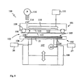
- Fig. 8 schematically illustrates a preferred embodiment of an apparatus according to the present invention, also usable for carrying out an embodiment of the method according to the present invention. It should be noted that this drawing is purely schematic, for the purpose of clarifying the different features thereof. In particular, dimensions of the different features are not on a common scale.
- the apparatus is particularly useful for carrying out the secondary step of the present invention, but may equally well be used for carrying out the primary step.
- the apparatus 100 comprises a first main part 101 and a second main part 102.
- these main parts are arranged with the first main part 101 on top of second main part, with an adjustable spacing 103 between said main parts.
- the first, upper, main part 101 has a downwards facing surface 104
- the second, lower, main part 102 has an upwards facing surface 105.
- Upwards facing surface 105 is, or has a portion that is, substantially flat, and which is placed on or forms part of a plate 106 which acts as a support structure for a template or a substrate to be used in an imprint process, as will be more thoroughly described in conjunction with Figs 9 and 10 .
- a heater body 21 is placed in contact with plate 106, or forms part of plate 106.
- Heater body 21 forms part of a heater device 20, and includes a heating element 22 and preferably also a cooling element 24, as shown in Figs 5-7 .
- Heating element 22 is connected through connectors 23 to a energy source 26, e.g. an electrical power supply with current control means.
- cooling element 24 is connected through connectors 25 to a cooling source 27, e.g. a cooling fluid reservoir and pump, with control means for controlling flow and temperature of the cooling fluid.
- Means for adjusting spacing 103 are, in the illustrated embodiment, provided by a piston member 107 attached at its outer end to plate 106. Piston member 107 is displaceably linked to a cylinder member 108, which preferably is held in fixed relation to first main part 101. As is indicated by the arrow in the drawing, the means for adjusting spacing 103 are devised to displace second main part 102 closer to or farther from first main part 101, by means of a movement substantially perpendicular to the substantially flat surface 105, i.e. in the Z direction. Displacement may be achieved manually, but is preferably assisted by employing either a hydraulic or pneumatic arrangement.
- the illustrated embodiment may be varied in a number of ways in this respect, for instance by instead attaching plate 106 to a cylinder member about a fixed piston member. It should further be noted that the displacement of second main part 102 is mainly employed for loading and unloading the apparatus 100 with a template and a substrate, and for arranging the apparatus in an initial operation position. The movement of second main part 102 is, however, preferably not included in the actual imprint process as such in the illustrated embodiment, as will be described.
- First main part 101 comprises a peripheral seal member 108, which encircles surface 104.
- seal member 108 is an endless seal such as an o-ring, but may alternatively be composed of several interconnected seal members which together form a continuous seal 108.
- Seal member 108 is disposed in a recess 109 outwardly of surface 104, and is preferably detachable from said recess.
- the apparatus further comprises a radiation source 110, in the illustrated embodiment disposed in the first main part 101 behind surface 104. Radiation source 110 is connectable to a radiation source driver 111, which preferably comprises or is connected to a power source (not shown). Radiation source driver 111 may be included in the apparatus 100, or be an external connectable member.
- a surface portion 112 of surface 104, disposed adjacent to radiation source 110, is formed in a material which is transparent to radiation of a certain wavelength or wavelength range of radiation source 110. This way, radiation emitted from radiation source 110 is transmitted towards spacing 103 between first main part 101 and second main part 102, through said surface portion 112.
- Surface portion 112, acting as a window, may be formed in available fused silica, quartz, or sapphire.
- One embodiment of the apparatus 100 according to the invention further comprises mechanical clamping means, for clamping together a substrate and a stamp (not shown). This is particularly preferred in an embodiment with an external alignment system for aligning substrate and stamp prior to pattern transfer, where the aligned stack comprising the stamp and the substrate has to be transferred into the imprint apparatus.
- apparatus 100 is further provided with a flexible membrane 113, which is substantially flat and engages seal member 108.
- seal member 113 is a separate member from seal member 108, and is only engaged with seal member 108 by applying a counter pressure from surface 105 of plate 106, as will be explained.
- membrane 113 is attached to seal member 108, e.g. by means of a cement, or by being an integral part of seal member 108.
- membrane 113 may be firmly attached to main part 101, whereas seal 108 is disposed outwardly of membrane 113.
- membrane 113 is formed in a material which is transparent to radiation of a certain wavelength or wavelength range of radiation source 110. This way, radiation emitted from radiation source 110 is transmitted into spacing 103 through said cavity 115 and its boundary walls 104 and 113.
- Examples of usable materials for membrane 113 include polycarbonate, polypropylene, polyethylene, PDMS and PEEK.
- the thickness of membrane 113 may typically be 10-500 ⁇ m.
- the apparatus 100 further preferably comprises means for applying a vacuum between stamp and substrate in order to extract air inclusions from the moldable layer of the stacked sandwich prior to hardening of the layer through UV irradiation.
- a vacuum pump 117 communicatively connected to the space between surface 105 and membrane 113 by a conduit 118.
- a conduit 114 is formed in first main part 101 for allowing a fluid medium, either a gas, a liquid or a gel, to pass to a space defined by surface 104, seal member 108 and membrane 113, which space acts as a cavity 115 for said fluid medium.
- Conduit 114 is connectable to a pressure source 116, such as a pump, which may be an external or a built in part of apparatus 100.
- Pressure source 116 is devised to apply an adjustable pressure, in particular an overpressure, to a fluid medium contained in said cavity 115.
- An embodiment such as the one illustrated is suitable for use with a gaseous pressure medium.
- said medium is selected from the group containing air, nitrogen, and argon.
- a liquid medium it is preferred to have the membrane attached to seal member 108.
- Such a liquid may be a hydraulic oil.
- Another possibility is to use a gel for said medium.
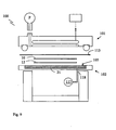
- Fig. 9 illustrates the apparatus embodiment of Fig. 8 , when being loaded with a substrate 12 and a polymer stamp 10 for a lithographic process.
- Second main part 102 has been displaced downwards from first main part 101, for opening up spacing 103.
- the illustrated embodiment of Fig. 8 shows an apparatus loaded with a transparent polymer stamp 10 on top of a substrate 12.
- Substrate 12 is placed with a backside thereof on surface 105 of heater body 21, placed on or in the second main part 102.
- substrate 12 has its target surface 17 with the layer 14 of a polymerizable material, e.g. a UV cross-linkable polymer solution, facing upwards.
- a polymerizable material e.g. a UV cross-linkable polymer solution
- Fig. 9 Polymer stamp 10 is placed on or adjacent to substrate 12, with its structured surface 11 facing substrate 12. Means for aligning polymer stamp 10 with substrate 12 may be provided, but are not illustrated in this schematic drawing. Membrane 113 is then placed on top of polymer stamp 10. For an embodiment where membrane 113 is attached to the first main part, the step of actually placing membrane 113 on the polymer stamp is, of course, dispensed with. In Fig. 9 polymer stamp 10, substrate 12 and membrane 113 are shown completely separated for the sake of clarity only, whereas in a real situation they would be stacked on surface 105.
- Fig. 10 illustrates an operative position of apparatus 100.
- Second main part 102 has been raised to a position where membrane 113 is clamped between seal member 108 and surface 105.
- both polymer stamp 10 and substrate 12 are very thin, typically only parts of a millimeter, and the actual bending of membrane 113 as illustrated is minimal.
- surface 105 may optionally be devised with a raised peripheral portion at the point where it contacts seal member 108 through membrane 113, for compensating for the combined thickness of polymer stamp 10 and substrate 12.
- cavity 115 is sealed. Vacuum is applied by suction from vacuum pump 117 to extract air inclusions from the surface layer of the substrate 12. Pressure source 116 is then devised to apply an overpressure to a fluid medium in cavity 115, which may be a gas, a liquid or a gel. The pressure in cavity 115 is transferred by membrane 113 to polymer stamp 10, which is pressed towards substrate 12 for imprinting the polymer stamp pattern in layer 14, cf. Fig. 6 .
- Cross-linkable polymer solutions typically need pre-heating to overcome its glass transition temperature T g , which may be about 60°C.
- T g glass transition temperature
- An example of such a polymer is the afore mr-L6000.1 XP.
- the apparatus 100 When using such polymers, the apparatus 100, having combined radiation and heating capabilities, is particularly useful. However, for both these types of materials a post-baking step is generally needed to harden the radiation-solidified layer 14'. As previously mentioned, an aspect of the invention is therefore to apply a raised temperature T p to the material of layer 14, which is higher than T g for the case of a cross-linkable material, and also suitable for postbaking of the radiation-exposed material. Heater device 20 is activated to heat layer 14 through substrate 12, by means of heater body 21, until T p has been reached. The actual value of T p is naturally dependent on the material chosen for layer 14.
- a temperature T p within the range of 50-150°C may be used, dependent on the molecular weight distribution in the material.
- the pressure of the medium in cavity 115 is then increased to 5-500 bar, advantageously to 5-200 bar, and preferably to 20-100 bar.
- Polymer stamp 10 and substrate 12 are thereby pressed together with a corresponding pressure. Thanks to flexible membrane 113, an absolutely even distribution of force is obtained over the whole of the contact surface between the substrate and the polymer stamp.
- the polymer stamp and the substrate are thereby made to arrange themselves absolutely parallel in relation to one another and, the influence of any irregularities in the surface of the substrate or polymer stamp being eliminated.
- radiation source is triggered to emit radiation 19.
- the radiation is transmitted through surface portion 112, which acts as a window, through cavity 115, membrane 113, and polymer stamp 10.
- the radiation is partly or completely absorbed in layer 14, the material of which thereby is solidified by cross-linking or curing in the perfectly parallel arrangement between polymer stamp 10 and substrate 12, provided by the pressure and membrane assisted compression.
- Radiation exposure time is dependent on the type and amount of material in layer 14, the radiation wavelength combined with the type of material, and of the radiation power.
- the feature of solidifying such a polymerizable material is well known as such, and the relevant combinations of the mentioned parameters are likewise known to the skilled person.
- the material of layer 14' is allowed to post bake, or hard bake, at the predetermined constant temperature T p for a certain time period of e.g. 1-10 minutes, if postbaking is at all necessary to solidify the layer.
- postbaking is typically performed for 1-10 minutes, preferably about 3 minutes, at the common process temperature T p of 100-120°C.
- the time of exposure to radiation is between 1 and 10 seconds, where the range of 3-5 seconds has been successfully tested, and postbaking is then performed at a T p of about 70°C for 30-60 seconds.
- post-baking is performed in the imprint machine 100, which means that it is not necessary to bring the substrate out of the apparatus and into a separate oven. This saves one process step, which makes both time and cost savings possible in the imprint process.
- T p a constant temperature
- the pressure in cavity 115 is reduced and the two main parts 101 and 102 are separated from one another. After this, the substrate is separated from the polymer stamp and subjected to further treatment according to what is previously known for imprint lithography.
- a first mode of the invention involves a substrate 12 of silicon covered by a layer 14 of NIP-K17 with a thickness of 1 ⁇ m.
- radiation source 110 is turned on.
- Radiation source 110 is typically devised to emit at least in the ultraviolet region below 400 nm.
- an air-cooled xenon lamp with an emission spectrum ranging from 200-1000 nm is employed as the radiation source 110.
- the preferred xenon type radiation source 110 provides a radiation of 1-10 W/cm 2 , and is devised to flash 1-5 ⁇ s pulses, with a pulse rate of 1-5 pulses per second.
- a window 112 of quartz is formed in surface 104 for passing through radiation. Exposure time is preferably between 1-30 seconds, for polymerizing fluid layer 14 into a solid layer 14', but may be up to 2 minutes.
- Tests with mr-L6000.1 XP have been performed with about 1.8 W/ cm 2 integrated from 200-1000 nm, with 1 minute exposure time. It should, in this context, be noted that the radiation used need not be restricted to a wavelength range within which the polymer applied in layer 14 solidifies, radiation outside that range may of course also be emitted from the radiation source used.
- second main part 102 is lowered to a position similar to that of Fig. 9 , following which template 10 and substrate 12 are removed from the apparatus for separation and further processing of the substrate.
- constant temperature is meant substantially constant, meaning that even though a temperature controller is set to maintain a certain temperature, the actual temperature obtained will inevitably fluctuate to a certain extent.
- the flexible properties of the used polymer foils alleviate complications of the pattern transfer due to different thermal expansion coefficients of the applied stamp and substrate materials used in the imprint-process. Therefore, the technique offers possibilities to transfer patterns between surfaces of materials characterized by different thermal expansion coefficients. Nevertheless, most polymers used in the application are characterized by quite similar thermal expansion factors typically ranging between 60 and 70 x 10 -6 C -1 making imprints between two different polymer foils as displayed in Fig. 1e ) more easy in terms of manufacturing.
- the flexible and ductile properties of the used polymer foils prevent the inclusion of air during the imprint between the polymer foil - having either a patterned or non-patterned surface - and the other object - e.g. a substrate covered by a polymer film or a template, comprising silicon, nickel, quartz or a polymer material. If the foil is pressed towards one of these objects as displayed in Fig. 1b, 1e, 1h the polymer foil is acting like a membrane, pressing the air from the centre of the imprinted area to its edges where it can leave the imprinted region.
- UV-curable polymers Due to the high transparency of the used polymer foils to e.g. UV-radiation, also UV-curable polymers can be used during the imprint process described above, even when non-transparent templates and substrates are used.
- Fig. 1 The process described above and displayed in Fig. 1 is very suitable to produce both positive (the pattern is similar to that of the original template) and negative (the pattern is inverted to that of the original template) replicas if the material properties of the different polymer materials - e.g. glass transition temperature, optical transparency, and curability after exposure to radiation - applied in the process are adapted to each other.
- material properties of the different polymer materials e.g. glass transition temperature, optical transparency, and curability after exposure to radiation - applied in the process are adapted to each other.
- the aging and wear resistance of the used flexible polymer stamps make it possible to apply them several times in the secondary step of the imprint process.
- the polymer stamps are used only once and are then thrown away. In any case, this enhances the lifetime of the original template 1, which never has to be used for imprint against a hard and non-flexible material.
- the flexible and ductile properties of the used polymer foils alleviate demolding of the inflexible stamp or substrate from the flexible foil reducing physical damages on the stamp or the substrate.
- the polymer foil can alternatively be chemically dissolved with the help of a suitable solvent. This procedure would be preferred in case of a transfer of patterns having high aspect ratios, i.e. where the depth of a pattern structure is substantially larger than its width, were mechanical demolding could damage the substrate or the stamp.
- the pattern on the surface of an original template can easily be transferred into a polymer foil.
- the placement of the pattern on the final substrate is critical.
- the master stamp can be produced with a centre hole. After imprint a relief of the centre hole is formed into the flexible polymer foil, which can be used for aligning the pattern on the foil to the final replicated disk.
- a replica generated in a polymer sheet can give access to a novel family development process, which is not executable the common way by nickel-to-nickel plating.
- the imprinted polymer sheet is first bonded together with a rigid substrate by, e.g., a UV-assisted imprint process. Thereafter the sheet is metallized with a seed layer and electroplated to receive a nickel copy of the original. Many other conversion process are accessible via the described invention.
- the invention as defined in the claims can be used in a method for transferring a pattern from a template having a structured surface to a target surface of a substrate, comprising:
- the step of releasing the substrate from the polymer stamp includes the step of dissolving the polymer stamp while still being arranged in contact with the imprinted intermediate layer on the substrate.
- said material is a cross-linkable thermoplastic polymer having an initial glass temperature T g , and wherein T p exceeds T g .
- said material is a UV cross-linkable thermoplastic polymer having a glass temperature T g , wherein temperature T p exceeds temperature T g , and wherein said radiation is UV radiation.
- said material is photo chemically amplified.
- the method comprises:
- said material is a UV-curable pre-polymer, and wherein said radiation is UV radiation.
- the method comprises:
- said medium comprises a gas
- said medium comprises air.
- said medium comprises a liquid.
- said medium comprises a gel.
- the method comprises:
- the method comprises:
- the method comprises:
- the step of exposing said layer comprises:
- the method comprises:
- the method comprises:
- the temperature T p is within the range of 20-250°C.
- the primary imprint step further includes
- the primary imprint step further includes
- the first polymer foil is made from a thermoplastic polymer or co-polymer material.
- the second polymer foil is made from a thermoplastic polymer or co-polymer material.
- the template is made from metal, quartz, polymer or silicon.
- the method comprises, while maintaining temperature T p :
- the method further comprises:
- the first polymer foil is made from polycarbonate, COC or PMMA.
- the primary imprint step is a thermal imprint process including
- the primary imprint step is a radiation-assisted imprint process including
- the primary imprint step further includes
- the primary imprint step is a radiation-assisted imprint process including
- the primary imprint step further includes
- the method further comprises the step of
- Zeonor ZF14 from Zeon Chemicals, Japan thermoplastic polymer having a glass temperature of 136°C and a light transmittance of 92% for wavelengths above 300 nm.
- the used foil has a thickness of 188 ⁇ m but is available in other thicknesses ranging from 50 to 500 ⁇ m.
- thermoplastic polymer having a glass temperature of 139°C and a light transmittance of 92% for wavelength above 350 nm.
- the used foil has a thickness of 75 ⁇ m.
- Polycarbonate (Bisphenol-A polycarbonate) from Bayer AG, Germany: thermoplastic polymer having a glass temperature of 150°C and a light transmittance of 91% for wavelength above 350 nm.
- the used foil has a thickness of 300 ⁇ m and is available in many other thicknesses up to 1 mm.
- a resist material which has been used is SU8 from MicroChem Corp. USA, a photo-resist material, curable after exposure to light having wavelengths between 350 and 400 nm.
- SU8 from MicroChem Corp. USA
- a photo-resist material curable after exposure to light having wavelengths between 350 and 400 nm.
- an adhesion promoter between the SU8 film and the silicon substrate a thin LOR0.7 film from MicroChem Corp. USA has been used.
- a nickel template whose surface exhibits a line pattern, having a line width of 80 nm and a height of 90 nm has been imprinted into a Zeonor ZF14 foil at 150°C and 50 bar for 3 min. None of the surfaces has been treated by any additional coating such as, e.g. anti-adhesion layers.
- the release temperature was 135°C, at which the Zeonor foil could mechanically be removed from the nickel surface without damaging the pattern of neither the template nor the replica.
- the Zeonor foil has been used as a new template, which has been imprinted into a 100 nm thick SU8 film.
- the SU8 film was spin-coated onto a 20nm LOR film, previously spin-coated onto a silicon substrate.
- the imprint was performed at 70°C and 50 bar for 3 min.
- the SU8 film was exposed to UV-light for 4 seconds through the optically transparent Zeonor foil and baked for two more minutes. Both temperature and pressure were kept constant at 70°C and 50 bar, respectively, during the entire imprint sequence.
- the release temperature was 70°C at which the Zeonor foil could mechanically be removed from the SU8 film without damaging the pattern of neither the polymer template foil nor the replica film.
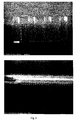
- the AFM image of an imprint result in the SU8 film deposited on a silicon wafer is shown in Fig. 2 .
- a nickel template whose surface exhibits a BluRay pattern having structure heights of 100 nm and widths of 150 nm - investigated by AFM - has been imprinted into a Zeonor ZF14 using the same process and the same parameters as already described in Example1.
- the Zeonor foil has been used as a new template, which has been imprinted into a 100 nm thick SU8 film. Also here the same process and the same parameters as already described in Example1 have been used.
- the AFM image of an imprint result in the SU8 film deposited on a silicon wafer is shown in Fig. 3 .
- a nickel template has been used whose surface contains micro-meter patterns with high aspect-ratios ranging from 1-28.
- the feature size ranges from 600 nm to 12 ⁇ m, at a height of 17 ⁇ m.
- the surface has been covered by a phosphate-based anti-adhesion film before the imprint.
- the nickel template has been imprinted into a polycarbonate foil at 190°C and 50 bar for 3 min.
- the surface of the polycarbonate foil has not been treated by an additional coating, having the purpose to improve the anti-adhesion behavior between the Ni template and the polycarbonate film.
- the release temperature was 130°C, at which the polycarbonate foil could mechanically be removed from the nickel surface without damaging the pattern of neither the template nor the replica.
- the polycarbonate foil has been used as a new template for an imprint into a Topas foil.
- the imprint has been performed at 120° C and 50 bar for 3 min. None of the surfaces has been disposed by an additional coating, having the purpose to improve the anti-adhesion behavior between the polycarbonate and the Topas foil.
- the release temperature was 70°C, at which the Topas could mechanically be removed from the polycarbonate foil without damaging the pattern of neither the template foil nor the replica foil.
- the Topas foil has then been used as a new template, which has been imprinted into a 6000 nm thick SU8 film spin-coated onto a silicon substrate.
- the Imprint processes given in the examples above have been performed with differently patterned Ni stamps, in some cases covered by phosphate-based anti-adhesion films, using different process parameters.
- the substrates (2 to 6 inch silicon wafers) have been cleaned by rinsing with isopropanol and acetone directly before spinning the LOR and the SU8 films.
- the sizes of the applied stamps are 2 to 6 inches.
- the imprints have been carried out using an Obducat-6-inch-NIL equipment, provided with an UV-module.
- Atomic force microscopy in the tapping mode with the help of a NanoScope IIIa microscope from Digital Instruments was carried out to investigate both the imprint results and the stamps after performed imprint.
Claims (18)
- Procédé de création d'un poinçon intermédiaire polymère (5 ; 8) pour l'utilisation dans un processus d'impression, dans lequel une surface à motif (4 ; 7) du poinçon intermédiaire polymère (5 ; 8) est pressée dans une couche déformable (14) sur un substrat (13) de façon à imprimer le motif de la surface à motif (4 ; 7) dans la couche déformable (14), ledit procédé comprenant :- prévoir un gabarit (1 ; 5) présentant une surface structurée (2 ; 4),- prévoir une feuille de polymère (3 ; 6),- prévoir une couche de surface de matériau prépolymère sensible aux rayonnements sur une surface de la feuille de polymère, dans lequel ledit matériau est amplifié par photochimie, dans lequel le matériau polymère est une composition polymère réticulable aux UV, et la feuille de polymère (3 ; 6) est préenduite de ladite composition polymère qui est solide à température ambiante normale,- presser la surface structurée (2 ; 4) dans ladite couche de surface pour imprimer une image inversée de ladite surface structurée (2 ; 4) dans la couche de surface,- chauffer la feuille de polymère (3 ; 6) à une température Tp, et, tout en maintenant ladite température Tp, exécuter ladite pression et ladite exposition, dans lequel ladite composition polymère présente une température de transition vitreuse initiale Tg, et dans lequel Tp dépasse Tg,- exposer la couche de surface à un rayonnement à travers la feuille de polymère pour durcir le prépolymère,- post-cuire la couche intermédiaire tout en maintenant une température Tp, et- séparer la feuille de polymère à motif (3 ; 6) du gabarit (1 ; 5), créant ainsi le poinçon intermédiaire polymère (5 ; 8).
- Procédé selon la revendication 1, dans lequel ladite exposition comprend en outre :- émettre ledit rayonnement vers la couche de surface à travers la feuille de polymère (3 ; 6), laquelle feuille de polymère est transparente à une plage de longueurs d'onde d'un rayonnement utilisable pour solidifier ladite seconde composition polymère.
- Procédé selon la revendication 1 ou 2, dans lequel ladite seconde composition polymère est un prépolymère durcissable aux UV.
- Procédé selon la revendication 3, dans lequel ladite étape consistant à prévoir une feuille de polymère comprend en outre :- distribuer la seconde composition polymère sur la surface structurée (2 ; 4) du gabarit (1 ; 5), et- couvrir la surface structurée (2 ; 4) avec la feuille de polymère, dans lequel ladite exposition amène la seconde composition polymère à adhérer sur la feuille de polymère.
- Procédé selon la revendication 3 ou 4, comprenant en outre :- prévoir de la chaleur pour post-cuire la couche de surface avant la séparation de la feuille de polymère à motif (3 ; 6) du gabarit (1 ; 5).
- Procédé selon une quelconque revendication précédente, dans lequel le gabarit (1 ; 5) est fabriqué en métal, quartz, polymère ou silicium.
- Procédé selon une quelconque revendication précédente, dans lequel ledit gabarit est un autre poinçon intermédiaire polymère (5) créé par une étape d'impression précédente comprenant :- prévoir une seconde feuille de polymère (3) présentant une feuille de polymère d'une troisième composition polymère et une couche de surface appliquée d'une quatrième composition polymère adaptée pour l'impression,- presser une surface structurée (2) d'un gabarit primaire (1) dans ladite couche de surface pour imprimer une reproduction de ladite surface structurée (2) dans la couche de surface,- exposer la couche de surface à un rayonnement pour solidifier la couche de surface, et- séparer la seconde feuille de polymère à motif (3) du gabarit, créant ainsi ledit autre poinçon intermédiaire polymère (5).
- Procédé selon la revendication 1, comprenant en outre :- disposer le gabarit (1 ; 5) et la feuille de polymère (3 ; 6) intercalés entre un élément d'arrêt et un premier côté d'une membrane flexible (113), et dans lequel- ladite pression implique l'application d'une surpression sur un milieu présent d'un second côté de la membrane (113).
- Procédé selon la revendication 8, dans lequel ledit milieu est sélectionné dans le groupe constitué d'un gaz, d'un liquide, et d'un gel.
- Procédé selon la revendication 8 ou 9, comprenant en outre :- émettre un rayonnement vers la couche de surface à travers la membrane (113), laquelle membrane est transparente à une plage de longueurs d'onde d'un rayonnement utilisable pour solidifier ladite seconde composition polymère.
- Procédé selon l'une quelconque des revendications 8 à 10, comprenant en outre :- émettre un rayonnement vers ladite couche de surface à travers ladite membrane (113), et à travers une paroi transparente (112) opposée à ladite membrane (113), définissant une paroi arrière pour une cavité (115) pour ledit milieu, lesquelles paroi arrière et membrane (113) sont transparentes à une plage de longueurs d'onde d'un rayonnement utilisable pour solidifier ladite seconde composition polymère.
- Procédé selon la revendication 8, dans lequel ladite exposition comprend en outre :- émettre un rayonnement à partir d'une source de rayonnement (110) dans une plage de longueurs d'onde de 100 à 500 nm.
- Procédé de formation d'un motif dans une surface cible d'un substrat, comprenant :une étape d'impression primaire incluant un procédé selon l'une quelconque des revendications 1 à 12 pour créer un poinçon intermédiaire polymère présentant une surface à motif, etune étape d'impression secondaire comprenant :- prévoir un substrat (13) présentant une couche déformable (14), et- presser le poinçon intermédiaire polymère (5 ; 8) dans la couche déformable (14) pour imprimer le motif de la surface à motif (4 ; 7) dans la couche déformable (14).
- Procédé selon la revendication 13, dans lequel ladite étape d'impression secondaire comprend en outre :- chauffer la couche déformable (14) au-dessus de sa température de transition vitreuse Tg, et- solidifier la couche déformable (14) en la refroidissant sous ladite température de transition vitreuse Tg.
- Procédé selon la revendication 13, dans lequel ladite étape d'impression secondaire comprend en outre :- exposer la couche déformable (14) à un rayonnement pour solidifier la couche déformable (14).
- Procédé selon la revendication 13, dans lequel ladite étape d'impression secondaire comprend en outre :- chauffer le poinçon intermédiaire polymère (5 ; 8) et le substrat (13) à une température Tp, et- effectuer, tout en maintenant ladite température Tp, ladite pression et une étape supplémentaire d'exposition de la couche déformable (14) à un rayonnement pour solidifier la couche déformable (14).
- Procédé selon la revendication 16, dans lequel ladite étape d'impression secondaire comprend en outre :- post-cuire la couche déformable (14) tout en maintenant ladite température Tp.
- Procédé selon la revendication 16 ou 17, dans lequel ladite étape d'impression secondaire comprend en outre :- libérer le substrat (13) du poinçon intermédiaire polymère (5 ; 8) tout en maintenant ladite température Tp.
Priority Applications (1)
| Application Number | Priority Date | Filing Date | Title |
|---|---|---|---|
| EP08154480A EP1959299B1 (fr) | 2005-06-10 | 2005-11-03 | Réplication de motif avec poinçon intermédiaire |
Applications Claiming Priority (4)
| Application Number | Priority Date | Filing Date | Title |
|---|---|---|---|
| US59515405P | 2005-06-10 | 2005-06-10 | |
| EP05105100A EP1731961B1 (fr) | 2005-06-10 | 2005-06-10 | Méthode pour la reproduction d'un modèle |
| EP08154480A EP1959299B1 (fr) | 2005-06-10 | 2005-11-03 | Réplication de motif avec poinçon intermédiaire |
| EP05110290A EP1731962B1 (fr) | 2005-06-10 | 2005-11-03 | Réplication d'un motif avec matrice de pressage intermédiaire |
Related Parent Applications (2)
| Application Number | Title | Priority Date | Filing Date |
|---|---|---|---|
| EP05110290.3 Division | 2005-11-03 | ||
| EP05110290A Division EP1731962B1 (fr) | 2005-06-10 | 2005-11-03 | Réplication d'un motif avec matrice de pressage intermédiaire |
Publications (3)
| Publication Number | Publication Date |
|---|---|
| EP1959299A2 EP1959299A2 (fr) | 2008-08-20 |
| EP1959299A3 EP1959299A3 (fr) | 2010-10-06 |
| EP1959299B1 true EP1959299B1 (fr) | 2012-12-26 |
Family
ID=35717449
Family Applications (2)
| Application Number | Title | Priority Date | Filing Date |
|---|---|---|---|
| EP08154480A Active EP1959299B1 (fr) | 2005-06-10 | 2005-11-03 | Réplication de motif avec poinçon intermédiaire |
| EP05110290A Active EP1731962B1 (fr) | 2005-06-10 | 2005-11-03 | Réplication d'un motif avec matrice de pressage intermédiaire |
Family Applications After (1)
| Application Number | Title | Priority Date | Filing Date |
|---|---|---|---|
| EP05110290A Active EP1731962B1 (fr) | 2005-06-10 | 2005-11-03 | Réplication d'un motif avec matrice de pressage intermédiaire |
Country Status (12)
| Country | Link |
|---|---|
| US (1) | US7704425B2 (fr) |
| EP (2) | EP1959299B1 (fr) |
| JP (1) | JP5276436B2 (fr) |
| KR (1) | KR101229100B1 (fr) |
| CN (1) | CN101198903B (fr) |
| AT (1) | ATE419560T1 (fr) |
| DE (1) | DE602005012068D1 (fr) |
| ES (1) | ES2317159T3 (fr) |
| HK (2) | HK1121243A1 (fr) |
| MY (1) | MY152606A (fr) |
| TW (2) | TWI313788B (fr) |
| WO (1) | WO2006131153A1 (fr) |
Families Citing this family (129)
| Publication number | Priority date | Publication date | Assignee | Title |
|---|---|---|---|---|
| EP1542074A1 (fr) * | 2003-12-11 | 2005-06-15 | Heptagon OY | Fabrication d'un outil de replication |
| US9040090B2 (en) | 2003-12-19 | 2015-05-26 | The University Of North Carolina At Chapel Hill | Isolated and fixed micro and nano structures and methods thereof |
| US20070228608A1 (en) * | 2006-04-03 | 2007-10-04 | Molecular Imprints, Inc. | Preserving Filled Features when Vacuum Wiping |
| US7854873B2 (en) | 2005-06-10 | 2010-12-21 | Obducat Ab | Imprint stamp comprising cyclic olefin copolymer |
| EP1731965B1 (fr) * | 2005-06-10 | 2012-08-08 | Obducat AB | Timbre d'impression comprenant un copolymère oléfine cyclique |
| US8184284B2 (en) | 2005-06-14 | 2012-05-22 | Ebstein Steven M | Laser-processed substrate for molecular diagnostics |
| US7715003B2 (en) | 2005-06-14 | 2010-05-11 | President & Fellows Of Harvard College | Metalized semiconductor substrates for raman spectroscopy |
| US7586601B2 (en) | 2005-06-14 | 2009-09-08 | Ebstein Steven M | Applications of laser-processed substrate for molecular diagnostics |
| JP2009509331A (ja) * | 2005-09-15 | 2009-03-05 | ダウ・コーニング・コーポレイション | ナノ成形法 |
| JP2007133970A (ja) * | 2005-11-10 | 2007-05-31 | Canon Inc | 光記録媒体およびその製造方法 |
| ATE549294T1 (de) * | 2005-12-09 | 2012-03-15 | Obducat Ab | Vorrichtung und verfahren zum transfer von mustern mit zwischenstempel |
| US7500431B2 (en) * | 2006-01-12 | 2009-03-10 | Tsai-Wei Wu | System, method, and apparatus for membrane, pad, and stamper architecture for uniform base layer and nanoimprinting pressure |
| US7377765B2 (en) * | 2006-02-14 | 2008-05-27 | Hitachi Global Storage Technologies | System, method, and apparatus for non-contact and diffuse curing exposure for making photopolymer nanoimprinting stamper |
| US7862756B2 (en) * | 2006-03-30 | 2011-01-04 | Asml Netherland B.V. | Imprint lithography |
| US20070257396A1 (en) * | 2006-05-05 | 2007-11-08 | Jian Wang | Device and method of forming nanoimprinted structures |
| US7998651B2 (en) | 2006-05-15 | 2011-08-16 | Asml Netherlands B.V. | Imprint lithography |
| US8318253B2 (en) * | 2006-06-30 | 2012-11-27 | Asml Netherlands B.V. | Imprint lithography |
| US20080047930A1 (en) * | 2006-08-23 | 2008-02-28 | Graciela Beatriz Blanchet | Method to form a pattern of functional material on a substrate |
| TW200839432A (en) * | 2006-12-05 | 2008-10-01 | Nano Terra Inc | Method for patterning a surface |
| US8608972B2 (en) | 2006-12-05 | 2013-12-17 | Nano Terra Inc. | Method for patterning a surface |
| US20100208237A1 (en) * | 2007-01-23 | 2010-08-19 | President & Fellows Of Harvard College | Polymeric substrates for raman spectroscopy |
| WO2008091858A2 (fr) | 2007-01-23 | 2008-07-31 | President & Fellows Of Harvard College | Analyse optique non invasive par spectroscopie de raman de surface améliorée |
| EP1982757A1 (fr) * | 2007-04-10 | 2008-10-22 | Stichting Voor De Technische Wetenschappen | Membrane laissant passer les ions et sa fabrication |
| WO2008149544A1 (fr) * | 2007-06-04 | 2008-12-11 | Scivax Corporation | Forme, article ayant subi un microtraitement et leurs procédés de fabrication |
| JP4448868B2 (ja) | 2007-06-29 | 2010-04-14 | 株式会社日立産機システム | インプリント用スタンパとその製造方法 |
| KR101415570B1 (ko) * | 2007-07-26 | 2014-07-04 | 삼성디스플레이 주식회사 | 임프린트 장치 및 이를 이용한 임프린트 방법 |
| US7864312B2 (en) | 2007-07-30 | 2011-01-04 | President And Fellows Of Harvard College | Substrates for Raman spectroscopy having discontinuous metal coatings |
| US20090056575A1 (en) * | 2007-08-31 | 2009-03-05 | Bartman Jon A | Pattern transfer apparatus |
| EP2205521A4 (fr) * | 2007-09-06 | 2013-09-11 | 3M Innovative Properties Co | Outil de fabrication d'articles à microstructures |
| US9440376B2 (en) | 2007-09-06 | 2016-09-13 | 3M Innovative Properties Company | Methods of forming molds and methods of forming articles using said molds |
| EP2198332A4 (fr) | 2007-09-06 | 2011-11-30 | 3M Innovative Properties Co | Guides de lumière ayant des structures d'extraction de lumière qui assurent un contrôle régional de sortie de lumière |
| CN101821302A (zh) * | 2007-10-11 | 2010-09-01 | 3M创新有限公司 | 高功能性多光子可固化反应性物质 |
| EP2208100B8 (fr) | 2007-10-11 | 2017-08-16 | 3M Innovative Properties Company | Détecteur confocal chromatique |
| WO2009075970A1 (fr) * | 2007-12-12 | 2009-06-18 | 3M Innovative Properties Company | Procédé de fabrication de structures présentant une définition de bordure améliorée |
| US20110039033A1 (en) * | 2008-01-31 | 2011-02-17 | Erika Merschrod | Method of depositing a polymer micropattern on a substrate |
| CN101960385B (zh) | 2008-02-26 | 2012-11-07 | 3M创新有限公司 | 多光子曝光系统 |
| US20110014499A1 (en) * | 2008-03-07 | 2011-01-20 | Showa Denko K.K. | Uv nanoimprint method, resin replica mold and method for producing the same, magnetic recording medium and method for producing the same, and magnetic recording/reproducing apparatus |
| JP4815464B2 (ja) * | 2008-03-31 | 2011-11-16 | 株式会社日立製作所 | 微細構造転写スタンパ及び微細構造転写装置 |
| JP5121549B2 (ja) * | 2008-04-21 | 2013-01-16 | 株式会社東芝 | ナノインプリント方法 |
| TWI416514B (zh) * | 2008-05-23 | 2013-11-21 | Showa Denko Kk | 樹脂模製作用疊層體、疊層體、樹脂模、及磁性記錄媒體的製造方法 |
| EP2138896B1 (fr) * | 2008-06-25 | 2014-08-13 | Obducat AB | Appareil et procédé de nano-impression |
| EP2300207A4 (fr) * | 2008-06-26 | 2012-05-09 | Harvard College | Matériaux nanostructurés actionnables, à rapport d'aspect élevé et polyvalent, par réplication |
| JP5638523B2 (ja) * | 2008-07-17 | 2014-12-10 | エージェンシー・フォー・サイエンス・テクノロジー・アンド・リサーチ | ポリマー構造上にインプリントを作製する方法 |
| JP2010080680A (ja) * | 2008-09-26 | 2010-04-08 | Bridgestone Corp | 凹凸パターンの形成方法及び凹凸パターンの製造装置 |
| US20100078846A1 (en) * | 2008-09-30 | 2010-04-01 | Molecular Imprints, Inc. | Particle Mitigation for Imprint Lithography |
| US9122148B2 (en) | 2008-11-03 | 2015-09-01 | Canon Nanotechnologies, Inc. | Master template replication |
| TWI421162B (zh) * | 2008-11-03 | 2014-01-01 | Molecular Imprints Inc | 母模板複製方法 |
| TWI508846B (zh) * | 2008-12-12 | 2015-11-21 | 麻省理工學院 | 不規則表面之楔形壓印圖案化 |
| EP2199855B1 (fr) | 2008-12-19 | 2016-07-20 | Obducat | Procédés et méthodes pour modifier les interactions en surface de matériaux polymériques |
| EP2199854B1 (fr) | 2008-12-19 | 2015-12-16 | Obducat AB | Moule en polymère hybride pour procédé de nanolithographie par impression, ainsi qu'un procédé pour sa fabrication |
| JP2010171338A (ja) * | 2009-01-26 | 2010-08-05 | Toshiba Corp | パターン生成方法及びパターン形成方法 |
| JP2010218605A (ja) | 2009-03-13 | 2010-09-30 | Toshiba Corp | パターン転写用紫外線硬化性樹脂材料、及びこれを用いた磁気記録媒体の製造方法 |
| JP4543117B1 (ja) * | 2009-03-13 | 2010-09-15 | 株式会社東芝 | パターン転写用紫外線硬化性樹脂材料、及びこれを用いた磁気記録媒体の製造方法 |
| JP2010218597A (ja) * | 2009-03-13 | 2010-09-30 | Toshiba Corp | パターン転写用樹脂スタンパ、及びこれを用いた磁気記録媒体の製造方法 |
| JP4729114B2 (ja) * | 2009-03-18 | 2011-07-20 | 株式会社東芝 | 磁気記録媒体の製造方法 |
| CN101900936A (zh) * | 2009-05-26 | 2010-12-01 | 鸿富锦精密工业(深圳)有限公司 | 压印模具及其制作方法 |
| US8178011B2 (en) * | 2009-07-29 | 2012-05-15 | Empire Technology Development Llc | Self-assembled nano-lithographic imprint masks |
| NL2005265A (en) | 2009-10-07 | 2011-04-11 | Asml Netherlands Bv | Imprint lithography apparatus and method. |
| JP5542404B2 (ja) * | 2009-10-08 | 2014-07-09 | 東レエンジニアリング株式会社 | マイクロニードルスタンパーの製造方法 |
| JP5558772B2 (ja) * | 2009-10-08 | 2014-07-23 | 東レエンジニアリング株式会社 | マイクロニードルシートのスタンパー及びその製造方法とそれを用いたマイクロニードルの製造方法 |
| US20120292820A1 (en) * | 2009-11-02 | 2012-11-22 | Nil Technology Aps | Method and device for nanoimprint lithography |
| US8980751B2 (en) * | 2010-01-27 | 2015-03-17 | Canon Nanotechnologies, Inc. | Methods and systems of material removal and pattern transfer |
| WO2011095217A1 (fr) | 2010-02-05 | 2011-08-11 | Obducat Ab | Procédé et processus permettant une reproduction de poinçon métallique pour des nanomotifs de grande surface |
| JP2011216808A (ja) * | 2010-04-02 | 2011-10-27 | Toshiba Mach Co Ltd | 転写装置、転写システム及び転写方法 |
| CN102958555A (zh) | 2010-04-28 | 2013-03-06 | 金伯利-克拉克环球有限公司 | 注射成型微针阵列和用于形成该微针阵列的方法 |
| WO2011139882A2 (fr) * | 2010-05-04 | 2011-11-10 | Unipixel Displays, Inc. | Procédé de fabrication de surfaces micro-structurées comprenant des motifs électriquement conducteurs |
| US9168679B2 (en) * | 2010-07-16 | 2015-10-27 | Northwestern University | Programmable soft lithography: solvent-assisted nanoscale embossing |
| US9688014B2 (en) * | 2010-09-01 | 2017-06-27 | Toshiba Kikai Kabushiki Kaisha | Transferring system and transferring method |
| US9034233B2 (en) * | 2010-11-30 | 2015-05-19 | Infineon Technologies Ag | Method of processing a substrate |
| TWI409161B (zh) * | 2010-12-10 | 2013-09-21 | Chenming Mold Ind Corp | 均壓成型模具及其均壓成型方法 |
| KR101200562B1 (ko) | 2011-01-17 | 2012-11-13 | 부산대학교 산학협력단 | 광정렬 일체형 대면적 금속 스탬프의 제조 방법 그리고 그를 이용한 고분자 광소자의 제조 방법 |
| EP2726299A4 (fr) * | 2011-06-30 | 2015-03-18 | 3M Innovative Properties Co | Procédé de fabrication, d'encrage et de montage de tampons pour impression par microcontact |
| KR20140054058A (ko) * | 2011-08-18 | 2014-05-08 | 모멘티브 퍼포먼스 머티리얼즈 게엠베하 | 조사 및 성형 유닛 |
| ES2908653T3 (es) | 2011-10-27 | 2022-05-03 | Sorrento Therapeutics Inc | Dispositivos implantables para la administración de agentes bioactivos |
| US9159925B2 (en) * | 2011-11-14 | 2015-10-13 | Orthogonal, Inc. | Process for imprint patterning materials in thin-film devices |
| JP5891075B2 (ja) | 2012-03-08 | 2016-03-22 | 東京応化工業株式会社 | ブロックコポリマー含有組成物及びパターンの縮小方法 |
| US10391485B2 (en) | 2013-09-25 | 2019-08-27 | Arizona Board Of Regents, A Body Corporate Of The State Of Arizona, Acting For And On Behalf Of Arizona State University | Microfluidic electrocage device and cell medium for trapping and rotating cells for live-cell computed tomography (CT) |
| US9513543B2 (en) | 2013-11-20 | 2016-12-06 | Eastman Kodak Company | Method for forming a non-deformable patterned template |
| US9193198B2 (en) | 2013-11-20 | 2015-11-24 | Eastman Kodak Company | PDMS imprinting stamp with embedded flexure |
| KR101617952B1 (ko) * | 2014-07-31 | 2016-05-09 | 한국과학기술원 | 소프트리소그래피를 이용한 경사진 관통 구멍을 구비한 구조체의 제조방법 |
| US10162162B2 (en) | 2014-09-24 | 2018-12-25 | Arizona Board Of Regents, A Body Corporate Of The State Of Arizona, Acting For And On Behalf Of Arizona State University | Microfluidic systems and methods for hydrodynamic microvortical cell rotation in live-cell computed tomography |
| JP2016164977A (ja) * | 2015-02-27 | 2016-09-08 | キヤノン株式会社 | ナノインプリント用液体材料、ナノインプリント用液体材料の製造方法、硬化物パターンの製造方法、光学部品の製造方法、回路基板の製造方法、および電子部品の製造方法 |
| CN107922183B (zh) | 2015-09-30 | 2022-09-13 | 富士胶片株式会社 | 铸模的制作方法、图案片材的制造方法、电铸模具的制作方法及使用了电铸模具的铸模的制作方法 |
| CN105399046A (zh) * | 2015-11-02 | 2016-03-16 | 中国科学院重庆绿色智能技术研究院 | 无机微光学元件批量化制作方法 |
| CN105372734B (zh) * | 2015-11-02 | 2018-01-19 | 中国科学院重庆绿色智能技术研究院 | 微棱镜反光材料制作方法 |
| WO2017195633A1 (fr) | 2016-05-09 | 2017-11-16 | デクセリアルズ株式会社 | Moule maître de réplique, procédé de fabrication d'un moule maître de réplique, article et procédé de fabrication d'un corps à former |
| JP6924006B2 (ja) | 2016-05-09 | 2021-08-25 | デクセリアルズ株式会社 | レプリカ原盤の製造方法、および被形成体の製造方法 |
| CN106500886B (zh) * | 2016-09-22 | 2019-05-10 | 太原理工大学 | 一种基于纳米导电材料的柔性应力传感器的制备方法 |
| US10969680B2 (en) * | 2016-11-30 | 2021-04-06 | Canon Kabushiki Kaisha | System and method for adjusting a position of a template |
| US10224224B2 (en) | 2017-03-10 | 2019-03-05 | Micromaterials, LLC | High pressure wafer processing systems and related methods |
| US10622214B2 (en) | 2017-05-25 | 2020-04-14 | Applied Materials, Inc. | Tungsten defluorination by high pressure treatment |
| US10847360B2 (en) | 2017-05-25 | 2020-11-24 | Applied Materials, Inc. | High pressure treatment of silicon nitride film |
| WO2018222771A1 (fr) | 2017-06-02 | 2018-12-06 | Applied Materials, Inc. | Décapage à sec de masque dur en carbure de bore |
| KR102246631B1 (ko) * | 2017-07-10 | 2021-04-30 | 주식회사 엘지화학 | 리튬 금속 전극용 3d 패턴 타발기 |
| US10234630B2 (en) * | 2017-07-12 | 2019-03-19 | Applied Materials, Inc. | Method for creating a high refractive index wave guide |
| JP6947914B2 (ja) | 2017-08-18 | 2021-10-13 | アプライド マテリアルズ インコーポレイテッドApplied Materials,Incorporated | 高圧高温下のアニールチャンバ |
| US10276411B2 (en) | 2017-08-18 | 2019-04-30 | Applied Materials, Inc. | High pressure and high temperature anneal chamber |
| CN111095524B (zh) | 2017-09-12 | 2023-10-03 | 应用材料公司 | 用于使用保护阻挡物层制造半导体结构的设备和方法 |
| JP2019056025A (ja) | 2017-09-19 | 2019-04-11 | 東芝メモリ株式会社 | パターン形成材料及びパターン形成方法 |
| CN107814353A (zh) * | 2017-10-26 | 2018-03-20 | 武汉大学 | 在透明柔性衬底上制备纳米针尖阵列的方法 |
| US10643867B2 (en) | 2017-11-03 | 2020-05-05 | Applied Materials, Inc. | Annealing system and method |
| KR102585074B1 (ko) | 2017-11-11 | 2023-10-04 | 마이크로머티어리얼즈 엘엘씨 | 고압 프로세싱 챔버를 위한 가스 전달 시스템 |
| US10854483B2 (en) | 2017-11-16 | 2020-12-01 | Applied Materials, Inc. | High pressure steam anneal processing apparatus |
| WO2019099255A2 (fr) | 2017-11-17 | 2019-05-23 | Applied Materials, Inc. | Système de condenseur pour système de traitement haute pression |
| CN111699549A (zh) | 2018-01-24 | 2020-09-22 | 应用材料公司 | 使用高压退火的接缝弥合 |
| SG11202008256WA (en) | 2018-03-09 | 2020-09-29 | Applied Materials Inc | High pressure annealing process for metal containing materials |
| RU183906U1 (ru) * | 2018-03-23 | 2018-10-08 | Акционерное общество "Центральный научно-исследовательский технологический институт "Техномаш" | Устройство для формирования планарной микроструктуры с рельефной поверхностью из фотоотверждаемой полимерной композиции методом контактного копирования |
| US10714331B2 (en) | 2018-04-04 | 2020-07-14 | Applied Materials, Inc. | Method to fabricate thermally stable low K-FinFET spacer |
| CN112041744A (zh) * | 2018-05-04 | 2020-12-04 | Ev 集团 E·索尔纳有限责任公司 | 印模和用于压印的方法 |
| US10950429B2 (en) | 2018-05-08 | 2021-03-16 | Applied Materials, Inc. | Methods of forming amorphous carbon hard mask layers and hard mask layers formed therefrom |
| US10566188B2 (en) | 2018-05-17 | 2020-02-18 | Applied Materials, Inc. | Method to improve film stability |
| KR102083308B1 (ko) * | 2018-05-23 | 2020-04-23 | 한국표준과학연구원 | 탐침형 원자 현미경을 이용한 리소그래피 방법 |
| US10704141B2 (en) | 2018-06-01 | 2020-07-07 | Applied Materials, Inc. | In-situ CVD and ALD coating of chamber to control metal contamination |
| CN109110728A (zh) * | 2018-07-25 | 2019-01-01 | 江西理工大学 | 基于离心力的微纳结构复制方法及制备得到的聚合物微纳结构 |
| US10748783B2 (en) | 2018-07-25 | 2020-08-18 | Applied Materials, Inc. | Gas delivery module |
| US10675581B2 (en) | 2018-08-06 | 2020-06-09 | Applied Materials, Inc. | Gas abatement apparatus |
| KR102528076B1 (ko) | 2018-10-30 | 2023-05-03 | 어플라이드 머티어리얼스, 인코포레이티드 | 반도체 응용들을 위한 구조를 식각하기 위한 방법들 |
| CN112996950B (zh) | 2018-11-16 | 2024-04-05 | 应用材料公司 | 使用增强扩散工艺的膜沉积 |
| CN109765687B (zh) * | 2018-12-04 | 2021-12-14 | 上海安翰医疗技术有限公司 | 曲面外壳上疏水涂层的制作方法及内窥镜 |
| WO2020117462A1 (fr) | 2018-12-07 | 2020-06-11 | Applied Materials, Inc. | Système de traitement de semi-conducteurs |
| DE102019101346A1 (de) | 2019-01-18 | 2020-07-23 | Osram Opto Semiconductors Gmbh | Nanostempelverfahren und nanooptisches bauteil |
| KR102237716B1 (ko) * | 2019-07-19 | 2021-04-08 | 한국과학기술원 | 미세 금속 마스크를 제작하는 방법 |
| CN110412684A (zh) * | 2019-08-01 | 2019-11-05 | 国家纳米科学中心 | 一种近眼显示器衍射光栅波导的制备方法 |
| CN111081624A (zh) * | 2019-11-28 | 2020-04-28 | 北京纳米能源与系统研究所 | 电子器件的柔性化方法 |
| CN111142329A (zh) * | 2019-12-16 | 2020-05-12 | 合肥元旭创芯半导体科技有限公司 | 一种非破坏性的半导体材料sem监控方法 |
| KR102217103B1 (ko) * | 2019-12-31 | 2021-02-18 | 전북대학교산학협력단 | 미세복합 표면구조의 제조방법 및 이를 이용한 미세복합 표면 탄성 폴리머 필름의 제조방법 |
| US11901222B2 (en) | 2020-02-17 | 2024-02-13 | Applied Materials, Inc. | Multi-step process for flowable gap-fill film |
| DE102020204766A1 (de) * | 2020-04-15 | 2021-10-21 | Robert Bosch Gesellschaft mit beschränkter Haftung | Verfahren zur Herstellung von Dämpferstrukturen an einem mikromechanischen Wafer |
| EP4057066A1 (fr) | 2021-03-11 | 2022-09-14 | Obducat AB | Appareil et procédé de traitement de surface d'un tampon d'impression |
Family Cites Families (41)
| Publication number | Priority date | Publication date | Assignee | Title |
|---|---|---|---|---|
| US2305433A (en) * | 1940-09-11 | 1942-12-15 | Jesse B Hawley | Method and apparatus for molding articles of thermoplastic, thermosetting, or resinous materials |
| BE479683A (fr) * | 1947-01-17 | |||
| JPS5772823A (en) * | 1980-10-27 | 1982-05-07 | Mitsui Toatsu Chem Inc | Production of duplicate disk for information recording |
| JPS62178309A (ja) * | 1986-01-31 | 1987-08-05 | Tanazawa Hatsukoushiya:Kk | マスタ除去方法 |
| DD251847A1 (de) * | 1986-07-31 | 1987-11-25 | Zeiss Jena Veb Carl | Verfahren und anordnung zum bildvergleich |
| JP2760381B2 (ja) * | 1988-12-09 | 1998-05-28 | 大日本印刷株式会社 | スタンパ |
| JPH02192045A (ja) * | 1989-01-20 | 1990-07-27 | Fujitsu Ltd | 光ディスク基板の製造方法 |
| JPH05114174A (ja) * | 1991-10-21 | 1993-05-07 | Ricoh Co Ltd | 光デイスク基板製造装置 |
| US5312794A (en) * | 1992-12-29 | 1994-05-17 | Shell Oil Company | Catalyst system for olefin polymerization |
| US5772905A (en) * | 1995-11-15 | 1998-06-30 | Regents Of The University Of Minnesota | Nanoimprint lithography |
| JPH09330864A (ja) * | 1996-06-10 | 1997-12-22 | Ge Yokogawa Medical Syst Ltd | 複合圧電物質製造方法及び複合圧電物質製造用マスク |
| JP3888485B2 (ja) * | 1997-06-27 | 2007-03-07 | 大日本インキ化学工業株式会社 | 紫外線硬化性組成物 |
| JP3577903B2 (ja) * | 1997-08-12 | 2004-10-20 | セイコーエプソン株式会社 | 樹脂板製造用鋳型の製造方法および樹脂板の製造方法 |
| JP2000071257A (ja) * | 1998-09-02 | 2000-03-07 | Kuraray Co Ltd | 成形品の製造方法 |
| US6334960B1 (en) | 1999-03-11 | 2002-01-01 | Board Of Regents, The University Of Texas System | Step and flash imprint lithography |
| SE515607C2 (sv) * | 1999-12-10 | 2001-09-10 | Obducat Ab | Anordning och metod vid tillverkning av strukturer |
| KR100694036B1 (ko) * | 2000-06-01 | 2007-03-12 | 삼성전자주식회사 | 그루브와 피트의 깊이가 다른 디스크 및 그 제조방법 |
| JP4192414B2 (ja) | 2000-09-14 | 2008-12-10 | 凸版印刷株式会社 | レンズシートの製造方法 |
| US6953332B1 (en) * | 2000-11-28 | 2005-10-11 | St. Jude Medical, Inc. | Mandrel for use in forming valved prostheses having polymer leaflets by dip coating |
| US6422528B1 (en) * | 2001-01-17 | 2002-07-23 | Sandia National Laboratories | Sacrificial plastic mold with electroplatable base |
| WO2002096166A1 (fr) * | 2001-05-18 | 2002-11-28 | Corporation For National Research Initiatives | Systemes microelectromecaniques (mems) radiofrequences sur substrats a ceramiques cocuites a basse temperature (ltcc) |
| US20030071016A1 (en) | 2001-10-11 | 2003-04-17 | Wu-Sheng Shih | Patterned structure reproduction using nonsticking mold |
| JP3749520B2 (ja) | 2002-01-08 | 2006-03-01 | Tdk株式会社 | 情報媒体製造用スタンパの製造方法、スタンパ、及び原盤付スタンパ中間体 |
| TWI258142B (en) * | 2002-01-08 | 2006-07-11 | Tdk Corp | Manufacturing method of stamper for manufacturing data medium, the stamper, and the stamper spacer with template |
| US6759180B2 (en) * | 2002-04-23 | 2004-07-06 | Hewlett-Packard Development Company, L.P. | Method of fabricating sub-lithographic sized line and space patterns for nano-imprinting lithography |
| US6849558B2 (en) * | 2002-05-22 | 2005-02-01 | The Board Of Trustees Of The Leland Stanford Junior University | Replication and transfer of microstructures and nanostructures |
| US20030230817A1 (en) * | 2002-06-13 | 2003-12-18 | Agere Systems, Inc. | Mold for UV curable adhesive and method of use therefor |
| US20040032063A1 (en) * | 2002-08-16 | 2004-02-19 | Peter Walther | Process for shaping plate-shaped materials and an arrangement for carrying out the process |
| JP2005537656A (ja) * | 2002-08-27 | 2005-12-08 | オブデュキャット、アクチボラグ | 対象物にパターンを転写するための装置 |
| JP2004109417A (ja) * | 2002-09-18 | 2004-04-08 | Dainippon Printing Co Ltd | 光回折構造の製造方法、複製版材、及び媒体 |
| JP4061220B2 (ja) * | 2003-03-20 | 2008-03-12 | 株式会社日立製作所 | ナノプリント装置、及び微細構造転写方法 |
| US20040241049A1 (en) * | 2003-04-04 | 2004-12-02 | Carvalho Bruce L. | Elastomeric tools for the fabrication of elastomeric devices and uses thereof |
| TW200507175A (en) * | 2003-06-20 | 2005-02-16 | Matsushita Electric Ind Co Ltd | Pattern forming method, and manufacturing method for semiconductor device |
| US7150844B2 (en) * | 2003-10-16 | 2006-12-19 | Seagate Technology Llc | Dry passivation process for stamper/imprinter family making for patterned recording media |
| US20050084804A1 (en) * | 2003-10-16 | 2005-04-21 | Molecular Imprints, Inc. | Low surface energy templates |
| US6939664B2 (en) * | 2003-10-24 | 2005-09-06 | International Business Machines Corporation | Low-activation energy silicon-containing resist system |
| DE60336322D1 (de) * | 2003-11-21 | 2011-04-21 | Obducat Ab | Nanoimprint Lithographie in Mehrschichtsystemem |
| DE102004005247A1 (de) * | 2004-01-28 | 2005-09-01 | Infineon Technologies Ag | Imprint-Lithographieverfahren |
| EP1594001B1 (fr) * | 2004-05-07 | 2015-12-30 | Obducat AB | Appareil et méthode pour la lithographie par empreinte |
| JP2008500914A (ja) | 2004-05-28 | 2008-01-17 | オブデュキャット、アクチボラグ | インプリント方法に使用する変性された金属製成形型 |
| US7163888B2 (en) * | 2004-11-22 | 2007-01-16 | Motorola, Inc. | Direct imprinting of etch barriers using step and flash imprint lithography |
-
2005
- 2005-11-03 DE DE602005012068T patent/DE602005012068D1/de active Active
- 2005-11-03 WO PCT/EP2005/055729 patent/WO2006131153A1/fr active Application Filing
- 2005-11-03 ES ES05110290T patent/ES2317159T3/es active Active
- 2005-11-03 EP EP08154480A patent/EP1959299B1/fr active Active
- 2005-11-03 JP JP2008515059A patent/JP5276436B2/ja active Active
- 2005-11-03 KR KR1020087000808A patent/KR101229100B1/ko active IP Right Grant
- 2005-11-03 AT AT05110290T patent/ATE419560T1/de active
- 2005-11-03 CN CN2005800500711A patent/CN101198903B/zh active Active
- 2005-11-03 EP EP05110290A patent/EP1731962B1/fr active Active
- 2005-11-07 MY MYPI20055204 patent/MY152606A/en unknown
- 2005-11-08 US US11/268,574 patent/US7704425B2/en active Active
- 2005-11-15 TW TW094140365A patent/TWI313788B/zh active
-
2006
- 2006-06-09 TW TW095120590A patent/TWI416280B/zh active
-
2007
- 2007-03-30 HK HK09100929.7A patent/HK1121243A1/xx unknown
- 2007-03-30 HK HK07103467.1A patent/HK1096162A1/xx unknown
Also Published As
| Publication number | Publication date |
|---|---|
| WO2006131153A1 (fr) | 2006-12-14 |
| US20060279025A1 (en) | 2006-12-14 |
| DE602005012068D1 (de) | 2009-02-12 |
| CN101198903B (zh) | 2011-09-07 |
| EP1731962A1 (fr) | 2006-12-13 |
| ES2317159T3 (es) | 2009-04-16 |
| MY152606A (en) | 2014-10-31 |
| KR101229100B1 (ko) | 2013-02-15 |
| EP1959299A3 (fr) | 2010-10-06 |
| TW200705123A (en) | 2007-02-01 |
| TWI416280B (zh) | 2013-11-21 |
| HK1121243A1 (en) | 2009-04-17 |
| EP1959299A2 (fr) | 2008-08-20 |
| TW200643613A (en) | 2006-12-16 |
| HK1096162A1 (en) | 2007-05-25 |
| JP2008542081A (ja) | 2008-11-27 |
| ATE419560T1 (de) | 2009-01-15 |
| US7704425B2 (en) | 2010-04-27 |
| KR20080023252A (ko) | 2008-03-12 |
| EP1731962B1 (fr) | 2008-12-31 |
| TWI313788B (en) | 2009-08-21 |
| CN101198903A (zh) | 2008-06-11 |
| JP5276436B2 (ja) | 2013-08-28 |
Similar Documents
| Publication | Publication Date | Title |
|---|---|---|
| EP1959299B1 (fr) | Réplication de motif avec poinçon intermédiaire | |
| US7670127B2 (en) | Apparatus for pattern replication with intermediate stamp | |
| US7854873B2 (en) | Imprint stamp comprising cyclic olefin copolymer | |
| US7972553B2 (en) | Method for imprint lithography at constant temperature | |
| KR101366505B1 (ko) | 고리형 올레핀 공중합체를 포함하는 임프린트 스탬프 | |
| JP2008542081A5 (fr) | ||
| JP5646692B2 (ja) | インプリント製法に使用される重合体スタンプの製造方法 | |
| US7363854B2 (en) | System and method for patterning both sides of a substrate utilizing imprint lithography | |
| JP4879511B2 (ja) | リソグラフィのための装置および方法 | |
| US20060180952A1 (en) | Imprint lithography | |
| EP1731965B1 (fr) | Timbre d'impression comprenant un copolymère oléfine cyclique | |
| KR101270082B1 (ko) | 인터미디어트 스탬프를 갖는 패턴 복제를 위한 장치 |
Legal Events
| Date | Code | Title | Description |
|---|---|---|---|
| PUAI | Public reference made under article 153(3) epc to a published international application that has entered the european phase |
Free format text: ORIGINAL CODE: 0009012 |
|
| AC | Divisional application: reference to earlier application |
Ref document number: 1731962 Country of ref document: EP Kind code of ref document: P |
|
| AK | Designated contracting states |
Kind code of ref document: A2 Designated state(s): AT BE BG CH CY CZ DE DK EE ES FI FR GB GR HU IE IS IT LI LT LU LV MC NL PL PT RO SE SI SK TR |
|
| RIN1 | Information on inventor provided before grant (corrected) |
Inventor name: BOLMSJOE, ERIK Inventor name: BECK, MARC Inventor name: HEIDARI, BABAK Inventor name: LOEFSTRAND, ANETTE Inventor name: THEANDER, ERIK |
|
| RIN1 | Information on inventor provided before grant (corrected) |
Inventor name: LOEFSTRAND, ANETTE Inventor name: BOLMSJOE, ERIK Inventor name: EHRENBORG, ERIK Inventor name: BECK, MARC Inventor name: HEIDARI, BABAK |
|
| REG | Reference to a national code |
Ref country code: HK Ref legal event code: DE Ref document number: 1121243 Country of ref document: HK |
|
| PUAL | Search report despatched |
Free format text: ORIGINAL CODE: 0009013 |
|
| AK | Designated contracting states |
Kind code of ref document: A3 Designated state(s): AT BE BG CH CY CZ DE DK EE ES FI FR GB GR HU IE IS IT LI LT LU LV MC NL PL PT RO SE SI SK TR |
|
| 17P | Request for examination filed |
Effective date: 20110405 |
|
| AKX | Designation fees paid |
Designated state(s): AT BE BG CH CY CZ DE DK EE ES FI FR GB GR HU IE IS IT LI LT LU LV MC NL PL PT RO SE SI SK TR |
|
| 17Q | First examination report despatched |
Effective date: 20120110 |
|
| RIC1 | Information provided on ipc code assigned before grant |
Ipc: G03F 7/00 20060101AFI20120628BHEP Ipc: B29C 59/02 20060101ALI20120628BHEP |
|
| GRAP | Despatch of communication of intention to grant a patent |
Free format text: ORIGINAL CODE: EPIDOSNIGR1 |
|
| GRAS | Grant fee paid |
Free format text: ORIGINAL CODE: EPIDOSNIGR3 |
|
| GRAA | (expected) grant |
Free format text: ORIGINAL CODE: 0009210 |
|
| AC | Divisional application: reference to earlier application |
Ref document number: 1731962 Country of ref document: EP Kind code of ref document: P |
|
| AK | Designated contracting states |
Kind code of ref document: B1 Designated state(s): AT BE BG CH CY CZ DE DK EE ES FI FR GB GR HU IE IS IT LI LT LU LV MC NL PL PT RO SE SI SK TR |
|
| REG | Reference to a national code |
Ref country code: GB Ref legal event code: FG4D |
|
| REG | Reference to a national code |
Ref country code: CH Ref legal event code: EP |
|
| REG | Reference to a national code |
Ref country code: AT Ref legal event code: REF Ref document number: 590774 Country of ref document: AT Kind code of ref document: T Effective date: 20130115 |
|
| REG | Reference to a national code |
Ref country code: DE Ref legal event code: R096 Ref document number: 602005037660 Country of ref document: DE Effective date: 20130228 |
|
| PG25 | Lapsed in a contracting state [announced via postgrant information from national office to epo] |
Ref country code: SE Free format text: LAPSE BECAUSE OF FAILURE TO SUBMIT A TRANSLATION OF THE DESCRIPTION OR TO PAY THE FEE WITHIN THE PRESCRIBED TIME-LIMIT Effective date: 20121226 Ref country code: FI Free format text: LAPSE BECAUSE OF FAILURE TO SUBMIT A TRANSLATION OF THE DESCRIPTION OR TO PAY THE FEE WITHIN THE PRESCRIBED TIME-LIMIT Effective date: 20121226 Ref country code: LT Free format text: LAPSE BECAUSE OF FAILURE TO SUBMIT A TRANSLATION OF THE DESCRIPTION OR TO PAY THE FEE WITHIN THE PRESCRIBED TIME-LIMIT Effective date: 20121226 |
|
| REG | Reference to a national code |
Ref country code: AT Ref legal event code: MK05 Ref document number: 590774 Country of ref document: AT Kind code of ref document: T Effective date: 20121226 |
|
| REG | Reference to a national code |
Ref country code: LT Ref legal event code: MG4D |
|
| REG | Reference to a national code |
Ref country code: NL Ref legal event code: VDEP Effective date: 20121226 |
|
| PG25 | Lapsed in a contracting state [announced via postgrant information from national office to epo] |
Ref country code: SI Free format text: LAPSE BECAUSE OF FAILURE TO SUBMIT A TRANSLATION OF THE DESCRIPTION OR TO PAY THE FEE WITHIN THE PRESCRIBED TIME-LIMIT Effective date: 20121226 Ref country code: LV Free format text: LAPSE BECAUSE OF FAILURE TO SUBMIT A TRANSLATION OF THE DESCRIPTION OR TO PAY THE FEE WITHIN THE PRESCRIBED TIME-LIMIT Effective date: 20121226 Ref country code: GR Free format text: LAPSE BECAUSE OF FAILURE TO SUBMIT A TRANSLATION OF THE DESCRIPTION OR TO PAY THE FEE WITHIN THE PRESCRIBED TIME-LIMIT Effective date: 20130327 |
|
| REG | Reference to a national code |
Ref country code: HK Ref legal event code: GR Ref document number: 1121243 Country of ref document: HK |
|
| PG25 | Lapsed in a contracting state [announced via postgrant information from national office to epo] |
Ref country code: SK Free format text: LAPSE BECAUSE OF FAILURE TO SUBMIT A TRANSLATION OF THE DESCRIPTION OR TO PAY THE FEE WITHIN THE PRESCRIBED TIME-LIMIT Effective date: 20121226 Ref country code: ES Free format text: LAPSE BECAUSE OF FAILURE TO SUBMIT A TRANSLATION OF THE DESCRIPTION OR TO PAY THE FEE WITHIN THE PRESCRIBED TIME-LIMIT Effective date: 20130406 Ref country code: AT Free format text: LAPSE BECAUSE OF FAILURE TO SUBMIT A TRANSLATION OF THE DESCRIPTION OR TO PAY THE FEE WITHIN THE PRESCRIBED TIME-LIMIT Effective date: 20121226 Ref country code: CZ Free format text: LAPSE BECAUSE OF FAILURE TO SUBMIT A TRANSLATION OF THE DESCRIPTION OR TO PAY THE FEE WITHIN THE PRESCRIBED TIME-LIMIT Effective date: 20121226 Ref country code: EE Free format text: LAPSE BECAUSE OF FAILURE TO SUBMIT A TRANSLATION OF THE DESCRIPTION OR TO PAY THE FEE WITHIN THE PRESCRIBED TIME-LIMIT Effective date: 20121226 Ref country code: CY Free format text: LAPSE BECAUSE OF FAILURE TO SUBMIT A TRANSLATION OF THE DESCRIPTION OR TO PAY THE FEE WITHIN THE PRESCRIBED TIME-LIMIT Effective date: 20121226 Ref country code: IS Free format text: LAPSE BECAUSE OF FAILURE TO SUBMIT A TRANSLATION OF THE DESCRIPTION OR TO PAY THE FEE WITHIN THE PRESCRIBED TIME-LIMIT Effective date: 20130426 Ref country code: BG Free format text: LAPSE BECAUSE OF FAILURE TO SUBMIT A TRANSLATION OF THE DESCRIPTION OR TO PAY THE FEE WITHIN THE PRESCRIBED TIME-LIMIT Effective date: 20130326 Ref country code: BE Free format text: LAPSE BECAUSE OF FAILURE TO SUBMIT A TRANSLATION OF THE DESCRIPTION OR TO PAY THE FEE WITHIN THE PRESCRIBED TIME-LIMIT Effective date: 20121226 |
|
| PG25 | Lapsed in a contracting state [announced via postgrant information from national office to epo] |
Ref country code: NL Free format text: LAPSE BECAUSE OF FAILURE TO SUBMIT A TRANSLATION OF THE DESCRIPTION OR TO PAY THE FEE WITHIN THE PRESCRIBED TIME-LIMIT Effective date: 20121226 Ref country code: PL Free format text: LAPSE BECAUSE OF FAILURE TO SUBMIT A TRANSLATION OF THE DESCRIPTION OR TO PAY THE FEE WITHIN THE PRESCRIBED TIME-LIMIT Effective date: 20121226 Ref country code: PT Free format text: LAPSE BECAUSE OF FAILURE TO SUBMIT A TRANSLATION OF THE DESCRIPTION OR TO PAY THE FEE WITHIN THE PRESCRIBED TIME-LIMIT Effective date: 20130426 Ref country code: RO Free format text: LAPSE BECAUSE OF FAILURE TO SUBMIT A TRANSLATION OF THE DESCRIPTION OR TO PAY THE FEE WITHIN THE PRESCRIBED TIME-LIMIT Effective date: 20121226 |
|
| PG25 | Lapsed in a contracting state [announced via postgrant information from national office to epo] |
Ref country code: DK Free format text: LAPSE BECAUSE OF FAILURE TO SUBMIT A TRANSLATION OF THE DESCRIPTION OR TO PAY THE FEE WITHIN THE PRESCRIBED TIME-LIMIT Effective date: 20121226 |
|
| PLBE | No opposition filed within time limit |
Free format text: ORIGINAL CODE: 0009261 |
|
| STAA | Information on the status of an ep patent application or granted ep patent |
Free format text: STATUS: NO OPPOSITION FILED WITHIN TIME LIMIT |
|
| 26N | No opposition filed |
Effective date: 20130927 |
|
| PG25 | Lapsed in a contracting state [announced via postgrant information from national office to epo] |
Ref country code: IT Free format text: LAPSE BECAUSE OF FAILURE TO SUBMIT A TRANSLATION OF THE DESCRIPTION OR TO PAY THE FEE WITHIN THE PRESCRIBED TIME-LIMIT Effective date: 20121226 |
|
| REG | Reference to a national code |
Ref country code: DE Ref legal event code: R097 Ref document number: 602005037660 Country of ref document: DE Effective date: 20130927 |
|
| REG | Reference to a national code |
Ref country code: CH Ref legal event code: PL |
|
| PG25 | Lapsed in a contracting state [announced via postgrant information from national office to epo] |
Ref country code: LI Free format text: LAPSE BECAUSE OF NON-PAYMENT OF DUE FEES Effective date: 20131130 Ref country code: CH Free format text: LAPSE BECAUSE OF NON-PAYMENT OF DUE FEES Effective date: 20131130 Ref country code: MC Free format text: LAPSE BECAUSE OF FAILURE TO SUBMIT A TRANSLATION OF THE DESCRIPTION OR TO PAY THE FEE WITHIN THE PRESCRIBED TIME-LIMIT Effective date: 20121226 |
|
| REG | Reference to a national code |
Ref country code: IE Ref legal event code: MM4A |
|
| PG25 | Lapsed in a contracting state [announced via postgrant information from national office to epo] |
Ref country code: IE Free format text: LAPSE BECAUSE OF NON-PAYMENT OF DUE FEES Effective date: 20131103 |
|
| PG25 | Lapsed in a contracting state [announced via postgrant information from national office to epo] |
Ref country code: TR Free format text: LAPSE BECAUSE OF FAILURE TO SUBMIT A TRANSLATION OF THE DESCRIPTION OR TO PAY THE FEE WITHIN THE PRESCRIBED TIME-LIMIT Effective date: 20121226 |
|
| PG25 | Lapsed in a contracting state [announced via postgrant information from national office to epo] |
Ref country code: LU Free format text: LAPSE BECAUSE OF NON-PAYMENT OF DUE FEES Effective date: 20131103 Ref country code: HU Free format text: LAPSE BECAUSE OF FAILURE TO SUBMIT A TRANSLATION OF THE DESCRIPTION OR TO PAY THE FEE WITHIN THE PRESCRIBED TIME-LIMIT; INVALID AB INITIO Effective date: 20051103 |
|
| REG | Reference to a national code |
Ref country code: FR Ref legal event code: PLFP Year of fee payment: 11 |
|
| REG | Reference to a national code |
Ref country code: FR Ref legal event code: PLFP Year of fee payment: 12 |
|
| REG | Reference to a national code |
Ref country code: FR Ref legal event code: PLFP Year of fee payment: 13 |
|
| REG | Reference to a national code |
Ref country code: FR Ref legal event code: PLFP Year of fee payment: 14 |
|
| PGFP | Annual fee paid to national office [announced via postgrant information from national office to epo] |
Ref country code: GB Payment date: 20231006 Year of fee payment: 19 |
|
| PGFP | Annual fee paid to national office [announced via postgrant information from national office to epo] |
Ref country code: FR Payment date: 20231024 Year of fee payment: 19 Ref country code: DE Payment date: 20231003 Year of fee payment: 19 |