EP1929556B1 - Reproducible resistance variable insulating memory devices and methods for forming same - Google Patents
Reproducible resistance variable insulating memory devices and methods for forming same Download PDFInfo
- Publication number
- EP1929556B1 EP1929556B1 EP06801233A EP06801233A EP1929556B1 EP 1929556 B1 EP1929556 B1 EP 1929556B1 EP 06801233 A EP06801233 A EP 06801233A EP 06801233 A EP06801233 A EP 06801233A EP 1929556 B1 EP1929556 B1 EP 1929556B1
- Authority
- EP
- European Patent Office
- Prior art keywords
- substrate
- forming
- electrode
- resistance variable
- memory element
- Prior art date
- Legal status (The legal status is an assumption and is not a legal conclusion. Google has not performed a legal analysis and makes no representation as to the accuracy of the status listed.)
- Not-in-force
Links
- 238000000034 method Methods 0.000 title claims description 32
- 239000000758 substrate Substances 0.000 claims description 39
- 239000004020 conductor Substances 0.000 claims description 24
- 239000000463 material Substances 0.000 claims description 17
- BASFCYQUMIYNBI-UHFFFAOYSA-N platinum Chemical compound [Pt] BASFCYQUMIYNBI-UHFFFAOYSA-N 0.000 claims description 12
- 238000000151 deposition Methods 0.000 claims description 9
- 238000005240 physical vapour deposition Methods 0.000 claims description 8
- 229910002353 SrRuO3 Inorganic materials 0.000 claims description 7
- 238000005229 chemical vapour deposition Methods 0.000 claims description 7
- GWEVSGVZZGPLCZ-UHFFFAOYSA-N Titan oxide Chemical compound O=[Ti]=O GWEVSGVZZGPLCZ-UHFFFAOYSA-N 0.000 claims description 6
- RTAQQCXQSZGOHL-UHFFFAOYSA-N Titanium Chemical compound [Ti] RTAQQCXQSZGOHL-UHFFFAOYSA-N 0.000 claims description 6
- PCHJSUWPFVWCPO-UHFFFAOYSA-N gold Chemical compound [Au] PCHJSUWPFVWCPO-UHFFFAOYSA-N 0.000 claims description 6
- 229910052737 gold Inorganic materials 0.000 claims description 6
- 239000010931 gold Substances 0.000 claims description 6
- ZKATWMILCYLAPD-UHFFFAOYSA-N niobium pentoxide Chemical compound O=[Nb](=O)O[Nb](=O)=O ZKATWMILCYLAPD-UHFFFAOYSA-N 0.000 claims description 6
- 229910052697 platinum Inorganic materials 0.000 claims description 6
- 229910052719 titanium Inorganic materials 0.000 claims description 6
- 239000010936 titanium Substances 0.000 claims description 6
- 229910002370 SrTiO3 Inorganic materials 0.000 claims description 5
- 238000004544 sputter deposition Methods 0.000 claims description 4
- 229910002113 barium titanate Inorganic materials 0.000 claims description 3
- 229910000473 manganese(VI) oxide Inorganic materials 0.000 claims description 3
- GNRSAWUEBMWBQH-UHFFFAOYSA-N nickel(II) oxide Inorganic materials [Ni]=O GNRSAWUEBMWBQH-UHFFFAOYSA-N 0.000 claims description 3
- 238000004549 pulsed laser deposition Methods 0.000 claims description 3
- 229910014031 strontium zirconium oxide Inorganic materials 0.000 claims description 3
- PBCFLUZVCVVTBY-UHFFFAOYSA-N tantalum pentoxide Inorganic materials O=[Ta](=O)O[Ta](=O)=O PBCFLUZVCVVTBY-UHFFFAOYSA-N 0.000 claims description 3
- 239000011810 insulating material Substances 0.000 abstract description 16
- 230000005684 electric field Effects 0.000 abstract description 3
- 239000004065 semiconductor Substances 0.000 description 18
- 239000010408 film Substances 0.000 description 9
- 230000015572 biosynthetic process Effects 0.000 description 5
- -1 for example Substances 0.000 description 4
- 230000003647 oxidation Effects 0.000 description 4
- 238000007254 oxidation reaction Methods 0.000 description 4
- 239000010409 thin film Substances 0.000 description 4
- 229910052751 metal Inorganic materials 0.000 description 3
- 239000002184 metal Substances 0.000 description 3
- 229910052581 Si3N4 Inorganic materials 0.000 description 2
- VYPSYNLAJGMNEJ-UHFFFAOYSA-N Silicium dioxide Chemical compound O=[Si]=O VYPSYNLAJGMNEJ-UHFFFAOYSA-N 0.000 description 2
- XUIMIQQOPSSXEZ-UHFFFAOYSA-N Silicon Chemical compound [Si] XUIMIQQOPSSXEZ-UHFFFAOYSA-N 0.000 description 2
- 230000008021 deposition Effects 0.000 description 2
- 229920002120 photoresistant polymer Polymers 0.000 description 2
- 238000000623 plasma-assisted chemical vapour deposition Methods 0.000 description 2
- 229910052710 silicon Inorganic materials 0.000 description 2
- 239000010703 silicon Substances 0.000 description 2
- HQVNEWCFYHHQES-UHFFFAOYSA-N silicon nitride Chemical compound N12[Si]34N5[Si]62N3[Si]51N64 HQVNEWCFYHHQES-UHFFFAOYSA-N 0.000 description 2
- 229910052814 silicon oxide Inorganic materials 0.000 description 2
- 230000004075 alteration Effects 0.000 description 1
- 238000003491 array Methods 0.000 description 1
- 239000000919 ceramic Substances 0.000 description 1
- 230000007547 defect Effects 0.000 description 1
- 238000005530 etching Methods 0.000 description 1
- 230000008020 evaporation Effects 0.000 description 1
- 238000001704 evaporation Methods 0.000 description 1
- 239000012212 insulator Substances 0.000 description 1
- 238000004519 manufacturing process Methods 0.000 description 1
- 238000000059 patterning Methods 0.000 description 1
- 230000002093 peripheral effect Effects 0.000 description 1
- 239000004033 plastic Substances 0.000 description 1
- 229910052594 sapphire Inorganic materials 0.000 description 1
- 239000010980 sapphire Substances 0.000 description 1
- 239000002904 solvent Substances 0.000 description 1
- 239000000126 substance Substances 0.000 description 1
- 238000006467 substitution reaction Methods 0.000 description 1
Images


Classifications
-
- H—ELECTRICITY
- H10—SEMICONDUCTOR DEVICES; ELECTRIC SOLID-STATE DEVICES NOT OTHERWISE PROVIDED FOR
- H10N—ELECTRIC SOLID-STATE DEVICES NOT OTHERWISE PROVIDED FOR
- H10N70/00—Solid-state devices having no potential barriers, and specially adapted for rectifying, amplifying, oscillating or switching
- H10N70/20—Multistable switching devices, e.g. memristors
-
- H—ELECTRICITY
- H10—SEMICONDUCTOR DEVICES; ELECTRIC SOLID-STATE DEVICES NOT OTHERWISE PROVIDED FOR
- H10N—ELECTRIC SOLID-STATE DEVICES NOT OTHERWISE PROVIDED FOR
- H10N70/00—Solid-state devices having no potential barriers, and specially adapted for rectifying, amplifying, oscillating or switching
- H10N70/011—Manufacture or treatment of multistable switching devices
- H10N70/061—Shaping switching materials
- H10N70/066—Shaping switching materials by filling of openings, e.g. damascene method
-
- H—ELECTRICITY
- H10—SEMICONDUCTOR DEVICES; ELECTRIC SOLID-STATE DEVICES NOT OTHERWISE PROVIDED FOR
- H10N—ELECTRIC SOLID-STATE DEVICES NOT OTHERWISE PROVIDED FOR
- H10N70/00—Solid-state devices having no potential barriers, and specially adapted for rectifying, amplifying, oscillating or switching
- H10N70/801—Constructional details of multistable switching devices
- H10N70/821—Device geometry
- H10N70/826—Device geometry adapted for essentially vertical current flow, e.g. sandwich or pillar type devices
-
- H—ELECTRICITY
- H10—SEMICONDUCTOR DEVICES; ELECTRIC SOLID-STATE DEVICES NOT OTHERWISE PROVIDED FOR
- H10N—ELECTRIC SOLID-STATE DEVICES NOT OTHERWISE PROVIDED FOR
- H10N70/00—Solid-state devices having no potential barriers, and specially adapted for rectifying, amplifying, oscillating or switching
- H10N70/801—Constructional details of multistable switching devices
- H10N70/841—Electrodes
- H10N70/8418—Electrodes adapted for focusing electric field or current, e.g. tip-shaped
-
- H—ELECTRICITY
- H10—SEMICONDUCTOR DEVICES; ELECTRIC SOLID-STATE DEVICES NOT OTHERWISE PROVIDED FOR
- H10N—ELECTRIC SOLID-STATE DEVICES NOT OTHERWISE PROVIDED FOR
- H10N70/00—Solid-state devices having no potential barriers, and specially adapted for rectifying, amplifying, oscillating or switching
- H10N70/801—Constructional details of multistable switching devices
- H10N70/881—Switching materials
- H10N70/883—Oxides or nitrides
- H10N70/8833—Binary metal oxides, e.g. TaOx
-
- H—ELECTRICITY
- H10—SEMICONDUCTOR DEVICES; ELECTRIC SOLID-STATE DEVICES NOT OTHERWISE PROVIDED FOR
- H10N—ELECTRIC SOLID-STATE DEVICES NOT OTHERWISE PROVIDED FOR
- H10N70/00—Solid-state devices having no potential barriers, and specially adapted for rectifying, amplifying, oscillating or switching
- H10N70/801—Constructional details of multistable switching devices
- H10N70/881—Switching materials
- H10N70/883—Oxides or nitrides
- H10N70/8836—Complex metal oxides, e.g. perovskites, spinels
Definitions
- the invention relates to the field of random access memory (RAM) devices formed using a resistance variable material, and in particular to an improved structure for, and a method of manufacturing, a resistance variable memory element.
- RAM random access memory
- Resistance variable memory is a RAM that has electrical resistance characteristics that can be changed by external influences.
- the basic component of a resistance variable memory cell is a variable resistor.
- the variable resistor can be programmed to have high resistance or low resistance (in two-state memory circuits), or any intermediate resistance value (in multi-state memory circuits).
- the different resistance values of the resistance variable memory cell represent the information stored in the resistance variable memory circuit.
- the advantages of resistance variable memory are the simplicity of the circuit, leading to smaller devices, the non-volatile characteristic of the memory cell, and the stability of the memory states.
- Word line contact via 116 is formed in dielectric layer 114. One end of word line contact via 116 is electrically connected to N+ region 106; the other end is electrically connected to a conducting line 120 on the surface of dielectric layer 114 so that the word line 102 can electrically connect with external circuits. Furthermore, there is a bit line 118 formed on dielectric layer 114 for electrically connecting with top electrode 110 of the memory unit 107.
- a second example of a conventional resistance variable memory device is a Type 1R1T (one resistor one transistor) memory device illustrated in FIG. 2 .
- This device includes a plurality of N+ regions 202 and 204 in substrate 200.
- a dielectric layer 220 is formed over substrate 200.
- Dielectric layer 220 includes a plurality of memory units 207, a plurality of gate structures (word lines) 212 and a plurality of contact vias 214 and 216.
- Each memory unit includes a flat plate bottom electrode 206, a flat plate top electrode 208 and a resistive film 210; which may be formed of one or more material layers, each memory unit is set on the surface of a respective N+ region.
- Gate structure 212 and N+ regions 202 and 204 constitute a transistor.
- Contact vias 214 and 216 are electrically connected to the gate structure 212 and the common line 204, respectively, so that the gate structure 212 and the common line 204 can connect with the external circuits. Furthermore, there is a bit line 218 formed on dielectric layer 220 for electrically connecting with the flat plate top electrode 208 of the memory unit 207.
- the metal-insulator-metal (MIM) structure with a resistive film or insulting oxide sandwiched between two flat metallic electrode plates as disclosed in FIGS. 1 and 2 does not provide stable and reproducible switching and does not provide memory properties in a controlled manner, as the conduction path between the elements can occur anywhere in the resistive film or insulating oxide between the top and bottom electrodes.
- the random and unpredictable conduction path between the elements is believed to be created by random and unpredictable defect sites in the deposited film.
- the present invention provides a memory element and a method of forming a memory element as claimed hereinafter.
- the present invention relates to the use of a shaped bottom electrode in a resistance variable memory device.
- the shaped bottom electrode ensures that the thickness of the insulating material at the tip of the bottom electrode is thinnest, therefore creating the largest electric field at the tip of the bottom electrode.
- the small curvature of the electrode tip also enhances the local electric field.
- the arrangement of electrodes and the structure of the memory element makes it possible to create conduction paths with stable, consistent and reproducible switching and memory properties in the memory device.
- FIG. 1 shows a cross-section of a conventional resistance random access memory device.
- FIG. 2 shows a cross-section of another conventional resistance random access memory device.
- FIG. 3 illustrates a partial cross-section of a memory device in accordance with an exemplary embodiment of the present invention.
- FIG. 4 illustrates a partial cross-section of a memory device in accordance with an second exemplary embodiment of the present invention.
- FIG. 5 illustrates a partial cross-section of a memory device in accordance with a third exemplary embodiment.
- FIG. 7 illustrates the semiconductor of FIG. 6 at a stage of processing subsequent to that shown in FIG. 6 .
- FIG. 8 illustrates the semiconductor of FIG. 6 at a stage of processing subsequent to that shown in FIG. 7 .
- FIG. 9 illustrates the semiconductor wafer of FIG. 6 at a stage of processing subsequent to that shown in FIG. 8 .
- FIG. 10 illustrates the semiconductor wafer of FIG. 6 at a stage of processing subsequent to that shown in FIG. 9 .
- FIG. 11 illustrates the semiconductor wafer of FIG. 6 at a stage of processing subsequent to that shown in FIG. 10 .
- FIG. 12 illustrates a cross-sectional view of a semiconductor wafer undergoing a second process for forming a memory device according to an exemplary embodiment of the present invention.
- FIG. 14 illustrates a cross-sectional view of a semiconductor wafer undergoing the process of forming a memory device according to an exemplary embodiment of a second embodiment of the present invention.
- FIG. 15 illustrates the semiconductor of FIG. 14 at a stage of processing subsequent to that shown in FIG. 14 .
- FIG. 16 illustrates the semiconductor of FIG. 14 at a stage of processing subsequent to that shown in FIG. 15 .
- FIG. 17 illustrates a processor-based system having a memory element formed according to the present invention.
- substrate used in the following description may include any supporting structure including, but not limited to, a plastic, ceramic, semiconductor, or other substrate that has an exposed substrate surface.
- a semiconductor substrate should be understood to include silicon, silicon-on-insulator (SOI), silicon-on-sapphire (SOS), doped and undoped semiconductors, epitaxial layers of silicon supported by a base semiconductor foundation, and other semiconductor material structures.
- SOI silicon-on-insulator
- SOS silicon-on-sapphire
- doped and undoped semiconductors epitaxial layers of silicon supported by a base semiconductor foundation, and other semiconductor material structures.
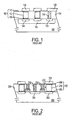
- a memory device 301 is schematically illustrated in FIG. 3 .
- the device 301 includes a shaped bottom electrode 308, a top electrode 310, a dielectric layer 314, and a resistance variable insulating material 312 between the shaped bottom electrode 308 and the top electrode 310.
- the resistance variable insulating material 312 is formed from resistance-reversible materials such as colossal magnetoresistive thin films, such as, for example a PCMO thin film (i.e., Pr 0.7 Ca 0.3 MnO 3 ); oxidation films having Perovskite structure, such as, for example, doped or undoped BaTiO 3 , SrTiO 3 or SrZrO 3 ; or an oxidation film such as, for example, Nb 2 O 5 , TiO 2 , Ta 2 O 5 , and NiO.
- the resistance variable insulating material 312 is SrTiO 3 .
- the shaped bottom electrode 308 and the top electrode 310 may be formed from a metal such as, for example, platinum, titanium or gold, or other suitable materials such as, for example, SrRuO 3 .
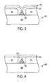
- FIG. 4 is similar to FIG. 3 and illustrates a memory device 303 where the resistance variable insulating material 312 has been planarized before the top electrode 310 has been formed over the substrate 300.
- FIG. 5 is similar to FIGS. 3 and 4 and illustrates a memory device 304 according to a third embodiment outside the scope of the claimed invention, where the bottom electrode 308 is formed over a conductive plug 322.
- resistance variable insulating material 312 has been planarized before the top electrode 310 has been formed over the substrate 300. It should be understood that the resistance variable insulating material 312 may simply be deposited and then have the top electrode 310 formed over the resistance variable insulating material 312, as discussed above with reference to FIG. 3 .
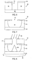
- FIGS. 6-11 depict the formation of the memory device 301 according to an exemplary embodiment of the invention. No particular order is required for any of the actions described herein, except for those logically requiring the results of prior actions. Accordingly, while the actions below are described as being performed in a general order, the order is exemplary only and can be altered if desired.
- FIG. 6 illustrates a dielectric layer 314 formed over the substrate 300.
- the dielectric layer 314 may be formed by any known deposition methods, such as sputtering by chemical vapor deposition (CVD), plasma enhanced CVD (PECVD) or physical vapor deposition (PVD).
- the dielectric layer 314 may be formed of a conventional insulating oxide, such as silicon oxide (SiO 2 ), a silicon nitride (Si 3 N 4 ); a low dielectric constant material; among others.
- a mask 316 is formed over the dielectric layer 314.
- the mask 316 is a photoresist mask; the mask 316, however, could instead be any other suitable material such as, for example, a metal.
- An opening 313 extending to the substrate 300 is formed in the dielectric layer 314 and mask 316.
- the opening 313 may be formed by known methods in the art, for example, by a conventional patterning and etching process.
- the opening 313 is formed by a dry etch via process to have substantially vertical sidewalls.
- a portion of the opening 313 is widened to form an opening 315 within the dielectric layer 314.
- the opening 315 extends under the mask 316, such that the opening 313 through the mask 316 is smaller than the opening 315 through the dielectric layer 314.
- the opening 315 is formed using a wet etch process.
- FIG. 8 depicts the formation of the shaped bottom electrode 308.
- a conductive material is deposited on the mask 316 and through the openings 313, 315 onto the substrate 300 to form a cone-like shaped bottom electrode 308 and a conductive layer 341 over the mask 316.
- the shaped bottom electrode 308 may comprise any conductive material, for example, platinum, titanium or gold, or other suitable materials such as, for example, SrRuO 3 .
- the conductive material is deposited by a physical vapor deposition (PVD) process, such as evaporation or collimated sputtering, but any suitable technique may be used. As indicated by arrow 351, the substrate 300 is rotated during deposition of the conductive material.
- PVD physical vapor deposition
- the conductive material is deposited in a single direction.
- the conductive material is deposited at an angle less than approximately 75 degrees with respect to the top surface of the substrate 300, but the conductive material can also deposited at an angle of approximately 75 degrees if desired.
- the shaped bottom electrode 308 By forming the shaped bottom electrode 308 using a PVD process, the seams or gaps that occur when an electrode is formed in the conventional chemical vapor deposition (CVD) plug process can be avoided. Additionally, PVD deposited material tends to have a smoother surface than CVD deposited material. Accordingly the shaped bottom electrode 308 may have a smoother surface than conventional electrodes.
- CVD chemical vapor deposition
- the conductive layer 341 and the mask 316 are removed, as illustrated in FIG. 9 .
- This can be accomplished by any suitable technique.
- a chemical mechanical polish (CMP) step can be conducted or a solvent lift-off process may be used according to known techniques.
- CMP chemical mechanical polish
- a resistance variable insulating material layer 312 is formed within the opening 315 and surrounding the shaped bottom electrode 308.
- the resistance variable insulating material layer 312 is formed from resistance-reversible materials such as colossal magnetoresistive thin films, such as, for example a PCMO thin film ( i.e ., Pr 0.7 Ca 0.3 MnO 3 ); oxidation films having Perovskite structure, such as, for example, doped or undoped BaTiO 3 , SrTiO 3 or SrZrO 3 ; or an oxidation film such as, for example, Nb 2 O 5 , TiO 2 , Ta 2 O 5 , and NiO.
- PCMO thin film i.e 0.7 Ca 0.3 MnO 3
- oxidation films having Perovskite structure such as, for example, doped or undoped BaTiO 3 , SrTiO 3 or SrZrO 3
- an oxidation film such as, for example, Nb 2 O
- the resistance variable insulating material 312 is SrTiO 3 .
- the resistance variable insulating material 312 is formed by known methods, such as, for example, pulsed laser deposition (PLD), PVD, sputtering, or CVD.
- a second electrode 310 is formed over the resistance variable insulating material layer 312.
- the second electrode 310 may comprise any electrically conductive material, for example, platinum, titanium or gold, or other suitable materials such as, for example, SrRuO 3 .
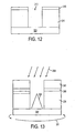
- FIGS. 12-13 illustrate another exemplary embodiment for forming the memory element 301 according to the invention.
- the embodiment illustrated in FIGS. 12-13 is similar to that described in FIGS. 6-11 , except that the second opening 315 ( FIG. 7 ) need not be formed.
- a mask 316 which may be a photoresist mask, is applied over dielectric layer 314 and substrate 300.
- An opening 313 extending to the substrate 300 is formed in the dielectric layer 314 and mask 316.
- the shaped bottom electrode 308 can be formed as described above in connection with FIG. 8 .
- a conductive material is deposited over the mask 316 and through the opening 313 onto the substrate 300 to form the shaped bottom electrode 308 and a conductive layer 341 over the mask 316 as illustrated in FIG. 13 .
- the substrate 300 is rotated during deposition of the conductive material.
- the conductive material is deposited in a single direction.
- the conductive material is deposited at an angle less than approximately 75 degrees with respect to the top surface of the substrate 300, but the conductive material can also deposited at an angle less of approximately 75 degrees.
- the memory device 301 is then processed as discussed above with reference to FIGS. 9-11 . Conventional processing steps can then be carried out to electrically couple the memory device 301 to various circuits of a memory array.
- FIGS. 14-16 depict the formation of the memory device 303 according to a second exemplary embodiment of the invention.
- FIG. 14 illustrates memory device which is processed as set forth above with reference to FIGS. 6-10 or 12-13.
- a CMP step is conducted to planarize the resistance variable insulating material layer 312 to achieve the structure shown in FIG. 15 .
- a second electrode 310 is formed over the resistance variable insulating material layer 312 as illustrated in FIG. 16 .
- the second electrode 310 may comprise any electrically conductive material, for example, platinum, titanium or gold, or other suitable materials such as, for example, SrRuO 3 .
- Conventional processing steps can then be carried out to electrically couple the memory device 301 to various circuits of a memory array.
- resistance variable memory element structures e.g., resistance variable memory devices
- the invention contemplates the formation of other memory structures within the claimed scope of the invention, which can be fabricated as a memory array and operated with memory element access circuits.
- FIG. 17 illustrates a processor system 700 which includes a memory circuit 748, e.g., a memory device, which employs resistance variable memory elements (e.g., elements 301 and/or 303 ( FIGS. 3 and 4 , respectively)) according to the invention.
- the processor system 700 which can be, for example, a computer system, generally comprises a central processing unit (CPU) 744, such as a microprocessor, a digital signal processor, or other programmable digital logic devices, which communicates with an input/output (I/O) device 746 over a bus 752.
- the memory circuit 748 communicates with the CPU 744 over bus 752 typically through a memory controller.
- the processor system 700 may include peripheral devices such as a floppy disk drive 754 and a compact disc (CD) ROM drive 756, which also communicate with CPU 744 over the bus 752.
- Memory circuit 748 is preferably constructed as an integrated circuit, which includes one or more resistance variable memory elements, e.g., elements 301 and/or 303. If desired, the memory circuit 748 may be combined with the processor, for example CPU 744, in a single integrated circuit.
Landscapes
- Engineering & Computer Science (AREA)
- Chemical & Material Sciences (AREA)
- Materials Engineering (AREA)
- Manufacturing & Machinery (AREA)
- Semiconductor Memories (AREA)
Priority Applications (1)
| Application Number | Priority Date | Filing Date | Title |
|---|---|---|---|
| EP11187300.6A EP2429007B1 (en) | 2005-08-15 | 2006-08-11 | Reproducible resistance variable insulating memory devices and methods for forming same |
Applications Claiming Priority (2)
| Application Number | Priority Date | Filing Date | Title |
|---|---|---|---|
| US11/203,141 US7521705B2 (en) | 2005-08-15 | 2005-08-15 | Reproducible resistance variable insulating memory devices having a shaped bottom electrode |
| PCT/US2006/031345 WO2007021913A1 (en) | 2005-08-15 | 2006-08-11 | Reproducible resistance variable insulating memory devices and methods for forming same |
Related Child Applications (2)
| Application Number | Title | Priority Date | Filing Date |
|---|---|---|---|
| EP11187300.6A Division EP2429007B1 (en) | 2005-08-15 | 2006-08-11 | Reproducible resistance variable insulating memory devices and methods for forming same |
| EP11187300.6 Division-Into | 2011-10-31 |
Publications (2)
| Publication Number | Publication Date |
|---|---|
| EP1929556A1 EP1929556A1 (en) | 2008-06-11 |
| EP1929556B1 true EP1929556B1 (en) | 2012-01-18 |
Family
ID=37562043
Family Applications (2)
| Application Number | Title | Priority Date | Filing Date |
|---|---|---|---|
| EP06801233A Not-in-force EP1929556B1 (en) | 2005-08-15 | 2006-08-11 | Reproducible resistance variable insulating memory devices and methods for forming same |
| EP11187300.6A Not-in-force EP2429007B1 (en) | 2005-08-15 | 2006-08-11 | Reproducible resistance variable insulating memory devices and methods for forming same |
Family Applications After (1)
| Application Number | Title | Priority Date | Filing Date |
|---|---|---|---|
| EP11187300.6A Not-in-force EP2429007B1 (en) | 2005-08-15 | 2006-08-11 | Reproducible resistance variable insulating memory devices and methods for forming same |
Country Status (8)
| Country | Link |
|---|---|
| US (4) | US7521705B2 (ja) |
| EP (2) | EP1929556B1 (ja) |
| JP (2) | JP5152674B2 (ja) |
| KR (1) | KR100954948B1 (ja) |
| CN (1) | CN101288187B (ja) |
| AT (1) | ATE542251T1 (ja) |
| TW (1) | TWI331794B (ja) |
| WO (1) | WO2007021913A1 (ja) |
Families Citing this family (98)
| Publication number | Priority date | Publication date | Assignee | Title |
|---|---|---|---|---|
| KR100697282B1 (ko) * | 2005-03-28 | 2007-03-20 | 삼성전자주식회사 | 저항 메모리 셀, 그 형성 방법 및 이를 이용한 저항 메모리배열 |
| US7521705B2 (en) | 2005-08-15 | 2009-04-21 | Micron Technology, Inc. | Reproducible resistance variable insulating memory devices having a shaped bottom electrode |
| US7491962B2 (en) * | 2005-08-30 | 2009-02-17 | Micron Technology, Inc. | Resistance variable memory device with nanoparticle electrode and method of fabrication |
| US8058636B2 (en) * | 2007-03-29 | 2011-11-15 | Panasonic Corporation | Variable resistance nonvolatile memory apparatus |
| US7768812B2 (en) | 2008-01-15 | 2010-08-03 | Micron Technology, Inc. | Memory cells, memory cell programming methods, memory cell reading methods, memory cell operating methods, and memory devices |
| US8211743B2 (en) | 2008-05-02 | 2012-07-03 | Micron Technology, Inc. | Methods of forming non-volatile memory cells having multi-resistive state material between conductive electrodes |
| US8134137B2 (en) | 2008-06-18 | 2012-03-13 | Micron Technology, Inc. | Memory device constructions, memory cell forming methods, and semiconductor construction forming methods |
| US9343665B2 (en) | 2008-07-02 | 2016-05-17 | Micron Technology, Inc. | Methods of forming a non-volatile resistive oxide memory cell and methods of forming a non-volatile resistive oxide memory array |
| US7795606B2 (en) * | 2008-08-05 | 2010-09-14 | Seagate Technology Llc | Non-volatile memory cell with enhanced filament formation characteristics |
| US7772583B2 (en) * | 2008-08-21 | 2010-08-10 | Micron Technology, Inc. | Memory devices and methods of forming the same |
| US8227783B2 (en) | 2009-07-13 | 2012-07-24 | Seagate Technology Llc | Non-volatile resistive sense memory with praseodymium calcium manganese oxide |
| US8048755B2 (en) * | 2010-02-08 | 2011-11-01 | Micron Technology, Inc. | Resistive memory and methods of processing resistive memory |
| US8427859B2 (en) | 2010-04-22 | 2013-04-23 | Micron Technology, Inc. | Arrays of vertically stacked tiers of non-volatile cross point memory cells, methods of forming arrays of vertically stacked tiers of non-volatile cross point memory cells, and methods of reading a data value stored by an array of vertically stacked tiers of non-volatile cross point memory cells |
| US8289763B2 (en) | 2010-06-07 | 2012-10-16 | Micron Technology, Inc. | Memory arrays |
| US9012307B2 (en) | 2010-07-13 | 2015-04-21 | Crossbar, Inc. | Two terminal resistive switching device structure and method of fabricating |
| US9601692B1 (en) | 2010-07-13 | 2017-03-21 | Crossbar, Inc. | Hetero-switching layer in a RRAM device and method |
| US9570678B1 (en) | 2010-06-08 | 2017-02-14 | Crossbar, Inc. | Resistive RAM with preferental filament formation region and methods |
| US8946046B1 (en) | 2012-05-02 | 2015-02-03 | Crossbar, Inc. | Guided path for forming a conductive filament in RRAM |
| WO2011156787A2 (en) | 2010-06-11 | 2011-12-15 | Crossbar, Inc. | Pillar structure for memory device and method |
| US8441835B2 (en) | 2010-06-11 | 2013-05-14 | Crossbar, Inc. | Interface control for improved switching in RRAM |
| JP5696378B2 (ja) * | 2010-06-15 | 2015-04-08 | ソニー株式会社 | 記憶装置の製造方法 |
| US8374018B2 (en) | 2010-07-09 | 2013-02-12 | Crossbar, Inc. | Resistive memory using SiGe material |
| US8467227B1 (en) | 2010-11-04 | 2013-06-18 | Crossbar, Inc. | Hetero resistive switching material layer in RRAM device and method |
| US8947908B2 (en) | 2010-11-04 | 2015-02-03 | Crossbar, Inc. | Hetero-switching layer in a RRAM device and method |
| US8569172B1 (en) | 2012-08-14 | 2013-10-29 | Crossbar, Inc. | Noble metal/non-noble metal electrode for RRAM applications |
| US8884261B2 (en) | 2010-08-23 | 2014-11-11 | Crossbar, Inc. | Device switching using layered device structure |
| US8168506B2 (en) | 2010-07-13 | 2012-05-01 | Crossbar, Inc. | On/off ratio for non-volatile memory device and method |
| US8889521B1 (en) | 2012-09-14 | 2014-11-18 | Crossbar, Inc. | Method for silver deposition for a non-volatile memory device |
| US8404553B2 (en) | 2010-08-23 | 2013-03-26 | Crossbar, Inc. | Disturb-resistant non-volatile memory device and method |
| US8492195B2 (en) | 2010-08-23 | 2013-07-23 | Crossbar, Inc. | Method for forming stackable non-volatile resistive switching memory devices |
| US9401475B1 (en) | 2010-08-23 | 2016-07-26 | Crossbar, Inc. | Method for silver deposition for a non-volatile memory device |
| US8558212B2 (en) | 2010-09-29 | 2013-10-15 | Crossbar, Inc. | Conductive path in switching material in a resistive random access memory device and control |
| US8391049B2 (en) | 2010-09-29 | 2013-03-05 | Crossbar, Inc. | Resistor structure for a non-volatile memory device and method |
| US8796661B2 (en) * | 2010-11-01 | 2014-08-05 | Micron Technology, Inc. | Nonvolatile memory cells and methods of forming nonvolatile memory cell |
| US8526213B2 (en) | 2010-11-01 | 2013-09-03 | Micron Technology, Inc. | Memory cells, methods of programming memory cells, and methods of forming memory cells |
| USRE46335E1 (en) | 2010-11-04 | 2017-03-07 | Crossbar, Inc. | Switching device having a non-linear element |
| US8502185B2 (en) | 2011-05-31 | 2013-08-06 | Crossbar, Inc. | Switching device having a non-linear element |
| US8088688B1 (en) | 2010-11-05 | 2012-01-03 | Crossbar, Inc. | p+ polysilicon material on aluminum for non-volatile memory device and method |
| US9454997B2 (en) | 2010-12-02 | 2016-09-27 | Micron Technology, Inc. | Array of nonvolatile memory cells having at least five memory cells per unit cell, having a plurality of the unit cells which individually comprise three elevational regions of programmable material, and/or having a continuous volume having a combination of a plurality of vertically oriented memory cells and a plurality of horizontally oriented memory cells; array of vertically stacked tiers of nonvolatile memory cells |
| US8431458B2 (en) | 2010-12-27 | 2013-04-30 | Micron Technology, Inc. | Methods of forming a nonvolatile memory cell and methods of forming an array of nonvolatile memory cells |
| US8930174B2 (en) | 2010-12-28 | 2015-01-06 | Crossbar, Inc. | Modeling technique for resistive random access memory (RRAM) cells |
| US8791010B1 (en) | 2010-12-31 | 2014-07-29 | Crossbar, Inc. | Silver interconnects for stacked non-volatile memory device and method |
| US9153623B1 (en) | 2010-12-31 | 2015-10-06 | Crossbar, Inc. | Thin film transistor steering element for a non-volatile memory device |
| US8815696B1 (en) | 2010-12-31 | 2014-08-26 | Crossbar, Inc. | Disturb-resistant non-volatile memory device using via-fill and etchback technique |
| US8791447B2 (en) | 2011-01-20 | 2014-07-29 | Micron Technology, Inc. | Arrays of nonvolatile memory cells and methods of forming arrays of nonvolatile memory cells |
| US8488365B2 (en) | 2011-02-24 | 2013-07-16 | Micron Technology, Inc. | Memory cells |
| CN102157692B (zh) * | 2011-03-22 | 2012-08-22 | 复旦大学 | 具有尖峰状底电极的有机阻变存储器的制备方法 |
| CN102157688B (zh) * | 2011-03-23 | 2012-07-18 | 北京大学 | 一种阻变存储器及其制备方法 |
| US8537592B2 (en) | 2011-04-15 | 2013-09-17 | Micron Technology, Inc. | Arrays of nonvolatile memory cells and methods of forming arrays of nonvolatile memory cells |
| US8450710B2 (en) | 2011-05-27 | 2013-05-28 | Crossbar, Inc. | Low temperature p+ silicon junction material for a non-volatile memory device |
| US9620206B2 (en) | 2011-05-31 | 2017-04-11 | Crossbar, Inc. | Memory array architecture with two-terminal memory cells |
| US8394670B2 (en) | 2011-05-31 | 2013-03-12 | Crossbar, Inc. | Vertical diodes for non-volatile memory device |
| US8619459B1 (en) | 2011-06-23 | 2013-12-31 | Crossbar, Inc. | High operating speed resistive random access memory |
| US8659929B2 (en) | 2011-06-30 | 2014-02-25 | Crossbar, Inc. | Amorphous silicon RRAM with non-linear device and operation |
| US9564587B1 (en) | 2011-06-30 | 2017-02-07 | Crossbar, Inc. | Three-dimensional two-terminal memory with enhanced electric field and segmented interconnects |
| US9166163B2 (en) | 2011-06-30 | 2015-10-20 | Crossbar, Inc. | Sub-oxide interface layer for two-terminal memory |
| US9627443B2 (en) | 2011-06-30 | 2017-04-18 | Crossbar, Inc. | Three-dimensional oblique two-terminal memory with enhanced electric field |
| US8946669B1 (en) | 2012-04-05 | 2015-02-03 | Crossbar, Inc. | Resistive memory device and fabrication methods |
| US9252191B2 (en) | 2011-07-22 | 2016-02-02 | Crossbar, Inc. | Seed layer for a p+ silicon germanium material for a non-volatile memory device and method |
| US8674724B2 (en) | 2011-07-29 | 2014-03-18 | Crossbar, Inc. | Field programmable gate array utilizing two-terminal non-volatile memory |
| US9729155B2 (en) | 2011-07-29 | 2017-08-08 | Crossbar, Inc. | Field programmable gate array utilizing two-terminal non-volatile memory |
| US10056907B1 (en) | 2011-07-29 | 2018-08-21 | Crossbar, Inc. | Field programmable gate array utilizing two-terminal non-volatile memory |
| WO2013028376A2 (en) * | 2011-08-24 | 2013-02-28 | Rambus Inc. | Resistive ram device having improved switching characteristics |
| US8716098B1 (en) | 2012-03-09 | 2014-05-06 | Crossbar, Inc. | Selective removal method and structure of silver in resistive switching device for a non-volatile memory device |
| US9087576B1 (en) | 2012-03-29 | 2015-07-21 | Crossbar, Inc. | Low temperature fabrication method for a three-dimensional memory device and structure |
| US9685608B2 (en) | 2012-04-13 | 2017-06-20 | Crossbar, Inc. | Reduced diffusion in metal electrode for two-terminal memory |
| US8658476B1 (en) | 2012-04-20 | 2014-02-25 | Crossbar, Inc. | Low temperature P+ polycrystalline silicon material for non-volatile memory device |
| US8796658B1 (en) | 2012-05-07 | 2014-08-05 | Crossbar, Inc. | Filamentary based non-volatile resistive memory device and method |
| US8765566B2 (en) | 2012-05-10 | 2014-07-01 | Crossbar, Inc. | Line and space architecture for a non-volatile memory device |
| US9583701B1 (en) | 2012-08-14 | 2017-02-28 | Crossbar, Inc. | Methods for fabricating resistive memory device switching material using ion implantation |
| US10096653B2 (en) | 2012-08-14 | 2018-10-09 | Crossbar, Inc. | Monolithically integrated resistive memory using integrated-circuit foundry compatible processes |
| US8946673B1 (en) | 2012-08-24 | 2015-02-03 | Crossbar, Inc. | Resistive switching device structure with improved data retention for non-volatile memory device and method |
| KR101922118B1 (ko) * | 2012-08-27 | 2018-11-26 | 삼성전자주식회사 | 플렉서블 반도체소자 및 그 제조방법 |
| US9312483B2 (en) | 2012-09-24 | 2016-04-12 | Crossbar, Inc. | Electrode structure for a non-volatile memory device and method |
| US9576616B2 (en) | 2012-10-10 | 2017-02-21 | Crossbar, Inc. | Non-volatile memory with overwrite capability and low write amplification |
| CN103730571B (zh) * | 2012-10-15 | 2018-07-27 | 马维尔国际贸易有限公司 | 在电阻式随机存取存储器单元中形成接触以降低单元编程所需电压的方法和装置 |
| US11068620B2 (en) | 2012-11-09 | 2021-07-20 | Crossbar, Inc. | Secure circuit integrated with memory layer |
| US8982647B2 (en) | 2012-11-14 | 2015-03-17 | Crossbar, Inc. | Resistive random access memory equalization and sensing |
| US9412790B1 (en) | 2012-12-04 | 2016-08-09 | Crossbar, Inc. | Scalable RRAM device architecture for a non-volatile memory device and method |
| CN103035840A (zh) | 2012-12-19 | 2013-04-10 | 北京大学 | 阻变存储器及其制备方法 |
| US9406379B2 (en) | 2013-01-03 | 2016-08-02 | Crossbar, Inc. | Resistive random access memory with non-linear current-voltage relationship |
| US9324942B1 (en) | 2013-01-31 | 2016-04-26 | Crossbar, Inc. | Resistive memory cell with solid state diode |
| US9112145B1 (en) | 2013-01-31 | 2015-08-18 | Crossbar, Inc. | Rectified switching of two-terminal memory via real time filament formation |
| US8934280B1 (en) | 2013-02-06 | 2015-01-13 | Crossbar, Inc. | Capacitive discharge programming for two-terminal memory cells |
| JP6092696B2 (ja) * | 2013-04-15 | 2017-03-08 | シャープ株式会社 | 可変抵抗素子を用いたメモリセル |
| US9608204B2 (en) * | 2013-09-09 | 2017-03-28 | Taiwan Semiconductor Manufacturing Company Ltd. | Resistive random access memory and manufacturing method thereof |
| CN103594622B (zh) * | 2013-11-28 | 2016-10-05 | 北京大学 | 高一致性的阻变存储器结构及其制备方法 |
| US10290801B2 (en) | 2014-02-07 | 2019-05-14 | Crossbar, Inc. | Scalable silicon based resistive memory device |
| US9245928B2 (en) | 2014-03-10 | 2016-01-26 | Kabushiki Kaisha Toshiba | Non-volatile memory device |
| JP2015065459A (ja) * | 2014-11-17 | 2015-04-09 | スパンション エルエルシー | 不揮発性メモリ用可変抵抗およびその製造方法並びに不揮発性メモリ |
| GB2561168B (en) * | 2017-03-31 | 2019-08-07 | Ucl Business Plc | A switching resistor and method of making such a device |
| CN107221598A (zh) * | 2017-04-25 | 2017-09-29 | 中国科学院微电子研究所 | 一种提高rram均一性的方法及rram器件 |
| US11730070B2 (en) | 2019-02-27 | 2023-08-15 | International Business Machines Corporation | Resistive random-access memory device with step height difference |
| CN109950394B (zh) * | 2019-03-29 | 2020-05-15 | 河南大学 | 无电形成过程阻变存储器实现量子电导效应的方法 |
| CN111463347A (zh) * | 2020-04-08 | 2020-07-28 | 电子科技大学 | 一种制备高性能忆阻器的方法 |
| CN111899916A (zh) * | 2020-08-04 | 2020-11-06 | 淮南师范学院 | 性能可变电极及其制备方法 |
| TW202306108A (zh) * | 2021-07-19 | 2023-02-01 | 聯華電子股份有限公司 | 電阻式隨機存取記憶體元件及其製造方法 |
| US11812675B2 (en) | 2021-09-21 | 2023-11-07 | International Business Machines Corporation | Filament confinement in resistive random access memory |
Family Cites Families (115)
| Publication number | Priority date | Publication date | Assignee | Title |
|---|---|---|---|---|
| EP0496215B1 (de) * | 1991-01-21 | 1995-08-30 | Siemens Aktiengesellschaft | Verfahren zur Herstellung eines strukturierten Aufbaus mit Hochtemperatursupraleitermaterial |
| JP2646999B2 (ja) * | 1994-04-26 | 1997-08-27 | 日本電気株式会社 | 電界放出型冷陰極 |
| JPH10506150A (ja) | 1994-08-01 | 1998-06-16 | フランツ ヘーマン、 | 非平衡軽量合金及び製品のために選択される処理 |
| US5869843A (en) * | 1995-06-07 | 1999-02-09 | Micron Technology, Inc. | Memory array having a multi-state element and method for forming such array or cells thereof |
| US6617205B1 (en) | 1995-11-20 | 2003-09-09 | Hitachi, Ltd. | Semiconductor storage device and process for manufacturing the same |
| JP3079987B2 (ja) | 1996-02-28 | 2000-08-21 | 日本電気株式会社 | 電界放出電子源およびその製造方法 |
| US5687112A (en) * | 1996-04-19 | 1997-11-11 | Energy Conversion Devices, Inc. | Multibit single cell memory element having tapered contact |
| JP3139375B2 (ja) * | 1996-04-26 | 2001-02-26 | 日本電気株式会社 | 電界放射冷陰極の製造方法 |
| DE69737086T2 (de) | 1996-08-27 | 2007-05-16 | Seiko Epson Corp. | Trennverfahren, verfahren zur übertragung eines dünnfilmbauelements, und unter verwendung des übertragungsverfahrens hergestelltes flüssigkristall-anzeigebauelement |
| US6147395A (en) * | 1996-10-02 | 2000-11-14 | Micron Technology, Inc. | Method for fabricating a small area of contact between electrodes |
| JP3139541B2 (ja) * | 1997-12-01 | 2001-03-05 | 日本電気株式会社 | 電界放出型冷陰極の製造方法 |
| US6150691A (en) | 1997-12-19 | 2000-11-21 | Micron Technology, Inc. | Spacer patterned, high dielectric constant capacitor |
| KR20010034127A (ko) | 1998-01-13 | 2001-04-25 | 조셉 제이. 스위니 | 이방성 플라티늄 프로화일을 위한 에칭 방법 |
| US6919168B2 (en) | 1998-01-13 | 2005-07-19 | Applied Materials, Inc. | Masking methods and etching sequences for patterning electrodes of high density RAM capacitors |
| US6323132B1 (en) | 1998-01-13 | 2001-11-27 | Applied Materials, Inc. | Etching methods for anisotropic platinum profile |
| CA2268469C (en) | 1998-04-10 | 2004-03-23 | University Of Central Florida | Apparatus and method for photocatalytic and thermocatalytic pollution control |
| US6280559B1 (en) | 1998-06-24 | 2001-08-28 | Sharp Kabushiki Kaisha | Method of manufacturing color electroluminescent display apparatus and method of bonding light-transmitting substrates |
| KR20000015469A (ko) * | 1998-08-29 | 2000-03-15 | 박이순 | 광중합형 감광성 형광체 페이스트 조성물및 이를 이용한 형광막의 형성방법 |
| US6869870B2 (en) | 1998-12-21 | 2005-03-22 | Megic Corporation | High performance system-on-chip discrete components using post passivation process |
| US7531417B2 (en) | 1998-12-21 | 2009-05-12 | Megica Corporation | High performance system-on-chip passive device using post passivation process |
| US8178435B2 (en) | 1998-12-21 | 2012-05-15 | Megica Corporation | High performance system-on-chip inductor using post passivation process |
| US6674619B2 (en) * | 1998-12-22 | 2004-01-06 | Rockwell Automation Technologies, Inc. | Method for interrupting an electrical circuit |
| US6815744B1 (en) * | 1999-02-17 | 2004-11-09 | International Business Machines Corporation | Microelectronic device for storing information with switchable ohmic resistance |
| US6297527B1 (en) | 1999-05-12 | 2001-10-02 | Micron Technology, Inc. | Multilayer electrode for ferroelectric and high dielectric constant capacitors |
| US6680900B1 (en) | 1999-06-04 | 2004-01-20 | Ricoh Company, Ltd. | Optical-pickup slider, manufacturing method thereof, probe and manufacturing method thereof, and probe array and manufacturing method thereof |
| JP2001158966A (ja) | 1999-12-01 | 2001-06-12 | Ebara Corp | 金属ないし金属化合物薄膜の作製方法 |
| US6565730B2 (en) | 1999-12-29 | 2003-05-20 | Intel Corporation | Self-aligned coaxial via capacitors |
| US6537715B2 (en) | 2000-07-28 | 2003-03-25 | Canon Kabushiki Kaisha | Toner, image-forming method and process cartridge |
| CN1196392C (zh) | 2000-07-31 | 2005-04-06 | 日本特殊陶业株式会社 | 布线基板及其制造方法 |
| KR100396879B1 (ko) | 2000-08-11 | 2003-09-02 | 삼성전자주식회사 | 동일 물질로 이루어진 이중막을 포함하는 다중막으로캡슐화된 캐패시터를 구비한 반도체 메모리 소자 및 그의제조 방법 |
| US6775150B1 (en) | 2000-08-30 | 2004-08-10 | Intel Corporation | Electronic assembly comprising ceramic/organic hybrid substrate with embedded capacitors and methods of manufacture |
| JP3664094B2 (ja) | 2000-10-18 | 2005-06-22 | 株式会社村田製作所 | 複合誘電体成形物、その製造方法、およびそれを用いたレンズアンテナ |
| EP1211333A3 (en) | 2000-12-01 | 2003-07-30 | Japan Pionics Co., Ltd. | Vaporizer for CVD apparatus |
| US7132666B2 (en) | 2001-02-07 | 2006-11-07 | Tomoji Takamasa | Radiation detector and radiation detecting element |
| KR100395766B1 (ko) | 2001-02-12 | 2003-08-25 | 삼성전자주식회사 | 강유전체 기억 소자 및 그 형성 방법 |
| US6686659B2 (en) | 2001-02-23 | 2004-02-03 | Intel Corporation | Selectable decoupling capacitors for integrated circuit and methods of use |
| WO2002096647A1 (en) | 2001-05-25 | 2002-12-05 | Advanced Ceramics Research, Inc. | Ceramic components having multilayered architectures and processes for manufacturing the same |
| KR20030002863A (ko) | 2001-06-30 | 2003-01-09 | 주식회사 하이닉스반도체 | 코어를 가진 플러그 구조 상의 강유전체 메모리소자 및 그제조방법 |
| US20030010992A1 (en) | 2001-07-16 | 2003-01-16 | Motorola, Inc. | Semiconductor structure and method for implementing cross-point switch functionality |
| US6596054B2 (en) | 2001-07-23 | 2003-07-22 | Advanced Technology Materials, Inc. | Method for carbon monoxide reduction during thermal/wet abatement of organic compounds |
| US6551381B2 (en) | 2001-07-23 | 2003-04-22 | Advanced Technology Materials, Inc. | Method for carbon monoxide reduction during thermal/wet abatement of organic compounds |
| WO2003010825A1 (en) | 2001-07-24 | 2003-02-06 | Seiko Epson Corporation | Transfer method, method of manufacturing thin film element, method of manufacturing integrated circuit, circuit substrate and method of manufacturing the circuit substrate, electro-optic device and method of manufacturing the electro-optic device, and ic card and electronic equipmen |
| US20030034491A1 (en) | 2001-08-14 | 2003-02-20 | Motorola, Inc. | Structure and method for fabricating semiconductor structures and devices for detecting an object |
| JP3912058B2 (ja) | 2001-08-21 | 2007-05-09 | ソニー株式会社 | 光ディスクおよびその製造方法 |
| US20030047765A1 (en) * | 2001-08-30 | 2003-03-13 | Campbell Kristy A. | Stoichiometry for chalcogenide glasses useful for memory devices and method of formation |
| KR20040038902A (ko) | 2001-10-10 | 2004-05-08 | 소니 가부시끼 가이샤 | 광학 렌즈, 집광 렌즈, 광학 픽업 및 광기록 재생 장치 |
| US6800563B2 (en) * | 2001-10-11 | 2004-10-05 | Ovonyx, Inc. | Forming tapered lower electrode phase-change memories |
| JP4149161B2 (ja) | 2001-12-06 | 2008-09-10 | 大日本印刷株式会社 | パターン形成体の製造方法およびパターン製造装置 |
| US6720553B2 (en) | 2002-01-17 | 2004-04-13 | Trustees Of The University Of Pennsylvania | Tip calibration standard and method for tip calibration |
| JP2004241396A (ja) * | 2002-02-07 | 2004-08-26 | Sharp Corp | 抵抗変化素子の製造方法および不揮発性抵抗変化メモリデバイスの製造方法、並びに不揮発性抵抗変化メモリデバイス |
| US7151273B2 (en) * | 2002-02-20 | 2006-12-19 | Micron Technology, Inc. | Silver-selenide/chalcogenide glass stack for resistance variable memory |
| KR100455287B1 (ko) | 2002-02-28 | 2004-11-06 | 삼성전자주식회사 | 반도체 장치의 커패시터, 그 제조방법 및 상기 커패시터를채용하고 있는 전자 소자 |
| US6713310B2 (en) | 2002-03-08 | 2004-03-30 | Samsung Electronics Co., Ltd. | Ferroelectric memory device using via etch-stop layer and method for manufacturing the same |
| US6534326B1 (en) * | 2002-03-13 | 2003-03-18 | Sharp Laboratories Of America, Inc. | Method of minimizing leakage current and improving breakdown voltage of polycrystalline memory thin films |
| US6849868B2 (en) * | 2002-03-14 | 2005-02-01 | Micron Technology, Inc. | Methods and apparatus for resistance variable material cells |
| US6670628B2 (en) * | 2002-04-04 | 2003-12-30 | Hewlett-Packard Company, L.P. | Low heat loss and small contact area composite electrode for a phase change media memory device |
| JP4103497B2 (ja) * | 2002-04-18 | 2008-06-18 | ソニー株式会社 | 記憶装置とその製造方法および使用方法、半導体装置とその製造方法 |
| JP3791509B2 (ja) | 2002-06-28 | 2006-06-28 | ソニー株式会社 | 光再生装置及び光再生方法 |
| AU2003241844A1 (en) * | 2002-07-11 | 2004-02-02 | Matsushita Electric Industrial Co., Ltd. | Nonvolatile memory and its manufacturing method |
| TWI233204B (en) * | 2002-07-26 | 2005-05-21 | Infineon Technologies Ag | Nonvolatile memory element and associated production methods and memory element arrangements |
| US6850429B2 (en) | 2002-08-02 | 2005-02-01 | Unity Semiconductor Corporation | Cross point memory array with memory plugs exhibiting a characteristic hysteresis |
| US6906939B2 (en) | 2002-08-02 | 2005-06-14 | Unity Semiconductor Corporation | Re-writable memory with multiple memory layers |
| US6836421B2 (en) | 2002-08-02 | 2004-12-28 | Unity Semiconductor Corporation | Line drivers that fit within a specified line pitch |
| US6856536B2 (en) | 2002-08-02 | 2005-02-15 | Unity Semiconductor Corporation | Non-volatile memory with a single transistor and resistive memory element |
| US6870755B2 (en) | 2002-08-02 | 2005-03-22 | Unity Semiconductor Corporation | Re-writable memory with non-linear memory element |
| US7326979B2 (en) | 2002-08-02 | 2008-02-05 | Unity Semiconductor Corporation | Resistive memory device with a treated interface |
| US7057914B2 (en) | 2002-08-02 | 2006-06-06 | Unity Semiconductor Corporation | Cross point memory array with fast access time |
| US7009909B2 (en) | 2002-08-02 | 2006-03-07 | Unity Semiconductor Corporation | Line drivers that use minimal metal layers |
| US6831854B2 (en) | 2002-08-02 | 2004-12-14 | Unity Semiconductor Corporation | Cross point memory array using distinct voltages |
| US6917539B2 (en) | 2002-08-02 | 2005-07-12 | Unity Semiconductor Corporation | High-density NVRAM |
| US6970375B2 (en) | 2002-08-02 | 2005-11-29 | Unity Semiconductor Corporation | Providing a reference voltage to a cross point memory array |
| US7042035B2 (en) | 2002-08-02 | 2006-05-09 | Unity Semiconductor Corporation | Memory array with high temperature wiring |
| US6859382B2 (en) | 2002-08-02 | 2005-02-22 | Unity Semiconductor Corporation | Memory array of a non-volatile ram |
| US7079442B2 (en) | 2002-08-02 | 2006-07-18 | Unity Semiconductor Corporation | Layout of driver sets in a cross point memory array |
| US6798685B2 (en) | 2002-08-02 | 2004-09-28 | Unity Semiconductor Corporation | Multi-output multiplexor |
| US7067862B2 (en) | 2002-08-02 | 2006-06-27 | Unity Semiconductor Corporation | Conductive memory device with conductive oxide electrodes |
| US6834008B2 (en) | 2002-08-02 | 2004-12-21 | Unity Semiconductor Corporation | Cross point memory array using multiple modes of operation |
| US7071008B2 (en) | 2002-08-02 | 2006-07-04 | Unity Semiconductor Corporation | Multi-resistive state material that uses dopants |
| US7020006B2 (en) | 2002-08-02 | 2006-03-28 | Unity Semiconductor Corporation | Discharge of conductive array lines in fast memory |
| US6850455B2 (en) | 2002-08-02 | 2005-02-01 | Unity Semiconductor Corporation | Multiplexor having a reference voltage on unselected lines |
| US7294417B2 (en) | 2002-09-12 | 2007-11-13 | The Trustees Of Boston College | Metal oxide nanostructures with hierarchical morphology |
| JP4323257B2 (ja) | 2002-09-24 | 2009-09-02 | コニカミノルタホールディングス株式会社 | 回路基板の製造方法、回路基板及び回路基板の製造装置 |
| JP3840207B2 (ja) | 2002-09-30 | 2006-11-01 | 株式会社東芝 | 絶縁膜及び電子素子 |
| JP2004158717A (ja) | 2002-11-07 | 2004-06-03 | Fujitsu Ltd | 薄膜積層体、その薄膜積層体を用いた電子装置及びアクチュエータ、並びにアクチュエータの製造方法 |
| JP4187197B2 (ja) * | 2002-11-07 | 2008-11-26 | シャープ株式会社 | 半導体メモリ装置の制御方法 |
| JP4298374B2 (ja) | 2002-11-18 | 2009-07-15 | シャープ株式会社 | 光情報記録媒体、並びに、それを用いた記録方法、再生方法、光情報記録装置、および光情報再生装置 |
| JP4381675B2 (ja) * | 2002-11-21 | 2009-12-09 | 富士通株式会社 | 半導体装置及びその製造方法、該半導体装置に係る測定用治具 |
| EP1429307B1 (en) | 2002-12-10 | 2005-06-22 | Askk Co.,Ltd. | Rotating braille display device |
| US7230316B2 (en) | 2002-12-27 | 2007-06-12 | Semiconductor Energy Laboratory Co., Ltd. | Semiconductor device having transferred integrated circuit |
| US6965128B2 (en) | 2003-02-03 | 2005-11-15 | Freescale Semiconductor, Inc. | Structure and method for fabricating semiconductor microresonator devices |
| EP1594176B1 (en) * | 2003-02-14 | 2010-05-19 | Fuji Electric Holdings Co., Ltd. | Switching device |
| US6868025B2 (en) | 2003-03-10 | 2005-03-15 | Sharp Laboratories Of America, Inc. | Temperature compensated RRAM circuit |
| US7063984B2 (en) * | 2003-03-13 | 2006-06-20 | Unity Semiconductor Corporation | Low temperature deposition of complex metal oxides (CMO) memory materials for non-volatile memory integrated circuits |
| TW200507218A (en) | 2003-03-31 | 2005-02-16 | North Corp | Layout circuit substrate, manufacturing method of layout circuit substrate, and circuit module |
| JP2004319049A (ja) | 2003-04-18 | 2004-11-11 | Sony Corp | 光記録媒体及びこれを用いた光記録再生方法 |
| JP4194504B2 (ja) | 2003-05-02 | 2008-12-10 | キヤノン株式会社 | 画像形成装置及び磁性トナー |
| TW589753B (en) | 2003-06-03 | 2004-06-01 | Winbond Electronics Corp | Resistance random access memory and method for fabricating the same |
| KR100773537B1 (ko) * | 2003-06-03 | 2007-11-07 | 삼성전자주식회사 | 한 개의 스위칭 소자와 한 개의 저항체를 포함하는비휘발성 메모리 장치 및 그 제조 방법 |
| JP3832659B2 (ja) | 2003-06-06 | 2006-10-11 | シャープ株式会社 | 光情報記録媒体、それを用いた記録方法、再生方法、光情報記録装置、および光情報再生装置 |
| JP4377617B2 (ja) | 2003-06-20 | 2009-12-02 | 日本特殊陶業株式会社 | コンデンサ、コンデンサ付き半導体素子、コンデンサ付き配線基板、および、半導体素子とコンデンサと配線基板とを備える電子ユニット |
| US6830938B1 (en) | 2003-06-24 | 2004-12-14 | Texas Instruments Incorporated | Method for improving retention reliability of ferroelectric RAM |
| JP2005026589A (ja) | 2003-07-04 | 2005-01-27 | Toshiba Corp | 半導体記憶装置及びその製造方法 |
| US7147834B2 (en) | 2003-08-11 | 2006-12-12 | The Research Foundation Of State University Of New York | Hydrothermal synthesis of perovskite nanotubes |
| JP4272486B2 (ja) | 2003-08-29 | 2009-06-03 | 東京エレクトロン株式会社 | 薄膜形成装置及び薄膜形成装置の洗浄方法 |
| JP4601552B2 (ja) | 2003-09-30 | 2010-12-22 | 株式会社日本触媒 | 複合誘電体用樹脂組成物および複合誘電体、該誘電体を使用した電気回路基板 |
| JPWO2005041303A1 (ja) * | 2003-10-23 | 2007-04-26 | 松下電器産業株式会社 | 抵抗変化素子、その製造方法、その素子を含むメモリ、およびそのメモリの駆動方法 |
| US7059664B2 (en) | 2003-12-04 | 2006-06-13 | General Motors Corporation | Airflow control devices based on active materials |
| US6849891B1 (en) | 2003-12-08 | 2005-02-01 | Sharp Laboratories Of America, Inc. | RRAM memory cell electrodes |
| JP2005203389A (ja) * | 2004-01-13 | 2005-07-28 | Sharp Corp | 不揮発性半導体記憶装置の製造方法 |
| DE102004007633B4 (de) | 2004-02-17 | 2010-10-14 | Qimonda Ag | Speicherzelle, Halbleiter-Speicherbauelement und Verfahren zur Herstellung einer Speicherzelle |
| JP4365737B2 (ja) * | 2004-06-30 | 2009-11-18 | シャープ株式会社 | 可変抵抗素子の駆動方法及び記憶装置 |
| US7791141B2 (en) | 2004-07-09 | 2010-09-07 | International Business Machines Corporation | Field-enhanced programmable resistance memory cell |
| US7374174B2 (en) * | 2004-12-22 | 2008-05-20 | Micron Technology, Inc. | Small electrode for resistance variable devices |
| US7208372B2 (en) | 2005-01-19 | 2007-04-24 | Sharp Laboratories Of America, Inc. | Non-volatile memory resistor cell with nanotip electrode |
| US7521705B2 (en) | 2005-08-15 | 2009-04-21 | Micron Technology, Inc. | Reproducible resistance variable insulating memory devices having a shaped bottom electrode |
-
2005
- 2005-08-15 US US11/203,141 patent/US7521705B2/en active Active
-
2006
- 2006-08-11 AT AT06801233T patent/ATE542251T1/de active
- 2006-08-11 EP EP06801233A patent/EP1929556B1/en not_active Not-in-force
- 2006-08-11 WO PCT/US2006/031345 patent/WO2007021913A1/en active Application Filing
- 2006-08-11 KR KR1020087006170A patent/KR100954948B1/ko not_active IP Right Cessation
- 2006-08-11 EP EP11187300.6A patent/EP2429007B1/en not_active Not-in-force
- 2006-08-11 JP JP2008527013A patent/JP5152674B2/ja not_active Expired - Fee Related
- 2006-08-11 CN CN200680035224.XA patent/CN101288187B/zh not_active Expired - Fee Related
- 2006-08-15 TW TW095129961A patent/TWI331794B/zh not_active IP Right Cessation
-
2009
- 2009-03-19 US US12/407,510 patent/US7863595B2/en active Active
-
2010
- 2010-11-24 US US12/954,160 patent/US8039300B2/en not_active Expired - Fee Related
-
2011
- 2011-09-29 US US13/248,214 patent/US8476613B2/en active Active
-
2012
- 2012-09-20 JP JP2012207558A patent/JP2013048251A/ja active Pending
Also Published As
| Publication number | Publication date |
|---|---|
| US8039300B2 (en) | 2011-10-18 |
| KR100954948B1 (ko) | 2010-04-27 |
| EP2429007B1 (en) | 2016-01-20 |
| EP2429007A3 (en) | 2014-09-03 |
| US20120018694A1 (en) | 2012-01-26 |
| KR20080044287A (ko) | 2008-05-20 |
| US20070034848A1 (en) | 2007-02-15 |
| JP5152674B2 (ja) | 2013-02-27 |
| EP2429007A2 (en) | 2012-03-14 |
| JP2009505424A (ja) | 2009-02-05 |
| US7863595B2 (en) | 2011-01-04 |
| JP2013048251A (ja) | 2013-03-07 |
| EP1929556A1 (en) | 2008-06-11 |
| CN101288187B (zh) | 2014-01-08 |
| US7521705B2 (en) | 2009-04-21 |
| US20090179188A1 (en) | 2009-07-16 |
| WO2007021913A1 (en) | 2007-02-22 |
| TW200713509A (en) | 2007-04-01 |
| US8476613B2 (en) | 2013-07-02 |
| US20110070714A1 (en) | 2011-03-24 |
| ATE542251T1 (de) | 2012-02-15 |
| TWI331794B (en) | 2010-10-11 |
| CN101288187A (zh) | 2008-10-15 |
Similar Documents
| Publication | Publication Date | Title |
|---|---|---|
| EP1929556B1 (en) | Reproducible resistance variable insulating memory devices and methods for forming same | |
| US7344946B2 (en) | Structure for amorphous carbon based non-volatile memory | |
| CN1967897B (zh) | 管型相变化存储器形成方法 | |
| US7289349B2 (en) | Resistance variable memory element with threshold device and method of forming the same | |
| US11088323B2 (en) | Top electrode last scheme for memory cell to prevent metal redeposit | |
| US10957742B2 (en) | Resistive random-access memory array with reduced switching resistance variability | |
| KR20030023556A (ko) | 메모리 셀 | |
| CN109841733B (zh) | 存储器件及其形成方法 | |
| JP2004363587A (ja) | 不完全に処理されるトンネル接合制御素子 | |
| US7663133B2 (en) | Memory elements having patterned electrodes and method of forming the same | |
| US20220085288A1 (en) | Rram bottom electrode | |
| CN114122254A (zh) | 具有多个输入端子的电阻式存储器元件 | |
| US20240260489A1 (en) | Method for forming a semiconductor memory device | |
| US20240324478A1 (en) | Rram bottom electrode | |
| US20230140134A1 (en) | Resistive random access memory device | |
| TW202236279A (zh) | 半導體記憶體元件及其製作方法 | |
| CN115472737A (zh) | 存储装置以及其制作方法 |
Legal Events
| Date | Code | Title | Description |
|---|---|---|---|
| PUAI | Public reference made under article 153(3) epc to a published international application that has entered the european phase |
Free format text: ORIGINAL CODE: 0009012 |
|
| 17P | Request for examination filed |
Effective date: 20080314 |
|
| AK | Designated contracting states |
Kind code of ref document: A1 Designated state(s): AT BE BG CH CY CZ DE DK EE ES FI FR GB GR HU IE IS IT LI LT LU LV MC NL PL PT RO SE SI SK TR |
|
| RIN1 | Information on inventor provided before grant (corrected) |
Inventor name: LIU, JUN |
|
| 17Q | First examination report despatched |
Effective date: 20091021 |
|
| GRAP | Despatch of communication of intention to grant a patent |
Free format text: ORIGINAL CODE: EPIDOSNIGR1 |
|
| DAX | Request for extension of the european patent (deleted) | ||
| GRAS | Grant fee paid |
Free format text: ORIGINAL CODE: EPIDOSNIGR3 |
|
| GRAA | (expected) grant |
Free format text: ORIGINAL CODE: 0009210 |
|
| AK | Designated contracting states |
Kind code of ref document: B1 Designated state(s): AT BE BG CH CY CZ DE DK EE ES FI FR GB GR HU IE IS IT LI LT LU LV MC NL PL PT RO SE SI SK TR |
|
| REG | Reference to a national code |
Ref country code: GB Ref legal event code: FG4D |
|
| REG | Reference to a national code |
Ref country code: CH Ref legal event code: EP |
|
| REG | Reference to a national code |
Ref country code: IE Ref legal event code: FG4D Ref country code: AT Ref legal event code: REF Ref document number: 542251 Country of ref document: AT Kind code of ref document: T Effective date: 20120215 |
|
| REG | Reference to a national code |
Ref country code: DE Ref legal event code: R096 Ref document number: 602006027208 Country of ref document: DE Effective date: 20120315 |
|
| REG | Reference to a national code |
Ref country code: NL Ref legal event code: VDEP Effective date: 20120118 |
|
| LTIE | Lt: invalidation of european patent or patent extension |
Effective date: 20120118 |
|
| PG25 | Lapsed in a contracting state [announced via postgrant information from national office to epo] |
Ref country code: BG Free format text: LAPSE BECAUSE OF FAILURE TO SUBMIT A TRANSLATION OF THE DESCRIPTION OR TO PAY THE FEE WITHIN THE PRESCRIBED TIME-LIMIT Effective date: 20120418 Ref country code: NL Free format text: LAPSE BECAUSE OF FAILURE TO SUBMIT A TRANSLATION OF THE DESCRIPTION OR TO PAY THE FEE WITHIN THE PRESCRIBED TIME-LIMIT Effective date: 20120118 Ref country code: IS Free format text: LAPSE BECAUSE OF FAILURE TO SUBMIT A TRANSLATION OF THE DESCRIPTION OR TO PAY THE FEE WITHIN THE PRESCRIBED TIME-LIMIT Effective date: 20120518 Ref country code: LT Free format text: LAPSE BECAUSE OF FAILURE TO SUBMIT A TRANSLATION OF THE DESCRIPTION OR TO PAY THE FEE WITHIN THE PRESCRIBED TIME-LIMIT Effective date: 20120118 Ref country code: BE Free format text: LAPSE BECAUSE OF FAILURE TO SUBMIT A TRANSLATION OF THE DESCRIPTION OR TO PAY THE FEE WITHIN THE PRESCRIBED TIME-LIMIT Effective date: 20120118 |
|
| PG25 | Lapsed in a contracting state [announced via postgrant information from national office to epo] |
Ref country code: GR Free format text: LAPSE BECAUSE OF FAILURE TO SUBMIT A TRANSLATION OF THE DESCRIPTION OR TO PAY THE FEE WITHIN THE PRESCRIBED TIME-LIMIT Effective date: 20120419 Ref country code: FI Free format text: LAPSE BECAUSE OF FAILURE TO SUBMIT A TRANSLATION OF THE DESCRIPTION OR TO PAY THE FEE WITHIN THE PRESCRIBED TIME-LIMIT Effective date: 20120118 Ref country code: PT Free format text: LAPSE BECAUSE OF FAILURE TO SUBMIT A TRANSLATION OF THE DESCRIPTION OR TO PAY THE FEE WITHIN THE PRESCRIBED TIME-LIMIT Effective date: 20120518 Ref country code: PL Free format text: LAPSE BECAUSE OF FAILURE TO SUBMIT A TRANSLATION OF THE DESCRIPTION OR TO PAY THE FEE WITHIN THE PRESCRIBED TIME-LIMIT Effective date: 20120118 Ref country code: LV Free format text: LAPSE BECAUSE OF FAILURE TO SUBMIT A TRANSLATION OF THE DESCRIPTION OR TO PAY THE FEE WITHIN THE PRESCRIBED TIME-LIMIT Effective date: 20120118 |
|
| REG | Reference to a national code |
Ref country code: AT Ref legal event code: MK05 Ref document number: 542251 Country of ref document: AT Kind code of ref document: T Effective date: 20120118 |
|
| PG25 | Lapsed in a contracting state [announced via postgrant information from national office to epo] |
Ref country code: CY Free format text: LAPSE BECAUSE OF FAILURE TO SUBMIT A TRANSLATION OF THE DESCRIPTION OR TO PAY THE FEE WITHIN THE PRESCRIBED TIME-LIMIT Effective date: 20120118 |
|
| PG25 | Lapsed in a contracting state [announced via postgrant information from national office to epo] |
Ref country code: RO Free format text: LAPSE BECAUSE OF FAILURE TO SUBMIT A TRANSLATION OF THE DESCRIPTION OR TO PAY THE FEE WITHIN THE PRESCRIBED TIME-LIMIT Effective date: 20120118 Ref country code: CZ Free format text: LAPSE BECAUSE OF FAILURE TO SUBMIT A TRANSLATION OF THE DESCRIPTION OR TO PAY THE FEE WITHIN THE PRESCRIBED TIME-LIMIT Effective date: 20120118 Ref country code: SI Free format text: LAPSE BECAUSE OF FAILURE TO SUBMIT A TRANSLATION OF THE DESCRIPTION OR TO PAY THE FEE WITHIN THE PRESCRIBED TIME-LIMIT Effective date: 20120118 Ref country code: SE Free format text: LAPSE BECAUSE OF FAILURE TO SUBMIT A TRANSLATION OF THE DESCRIPTION OR TO PAY THE FEE WITHIN THE PRESCRIBED TIME-LIMIT Effective date: 20120118 Ref country code: DK Free format text: LAPSE BECAUSE OF FAILURE TO SUBMIT A TRANSLATION OF THE DESCRIPTION OR TO PAY THE FEE WITHIN THE PRESCRIBED TIME-LIMIT Effective date: 20120118 Ref country code: EE Free format text: LAPSE BECAUSE OF FAILURE TO SUBMIT A TRANSLATION OF THE DESCRIPTION OR TO PAY THE FEE WITHIN THE PRESCRIBED TIME-LIMIT Effective date: 20120118 |
|
| PLBE | No opposition filed within time limit |
Free format text: ORIGINAL CODE: 0009261 |
|
| STAA | Information on the status of an ep patent application or granted ep patent |
Free format text: STATUS: NO OPPOSITION FILED WITHIN TIME LIMIT |
|
| PG25 | Lapsed in a contracting state [announced via postgrant information from national office to epo] |
Ref country code: IT Free format text: LAPSE BECAUSE OF FAILURE TO SUBMIT A TRANSLATION OF THE DESCRIPTION OR TO PAY THE FEE WITHIN THE PRESCRIBED TIME-LIMIT Effective date: 20120118 Ref country code: SK Free format text: LAPSE BECAUSE OF FAILURE TO SUBMIT A TRANSLATION OF THE DESCRIPTION OR TO PAY THE FEE WITHIN THE PRESCRIBED TIME-LIMIT Effective date: 20120118 |
|
| 26N | No opposition filed |
Effective date: 20121019 |
|
| PG25 | Lapsed in a contracting state [announced via postgrant information from national office to epo] |
Ref country code: AT Free format text: LAPSE BECAUSE OF FAILURE TO SUBMIT A TRANSLATION OF THE DESCRIPTION OR TO PAY THE FEE WITHIN THE PRESCRIBED TIME-LIMIT Effective date: 20120118 |
|
| REG | Reference to a national code |
Ref country code: DE Ref legal event code: R097 Ref document number: 602006027208 Country of ref document: DE Effective date: 20121019 |
|
| REG | Reference to a national code |
Ref country code: CH Ref legal event code: PL |
|
| PG25 | Lapsed in a contracting state [announced via postgrant information from national office to epo] |
Ref country code: MC Free format text: LAPSE BECAUSE OF NON-PAYMENT OF DUE FEES Effective date: 20120831 |
|
| PG25 | Lapsed in a contracting state [announced via postgrant information from national office to epo] |
Ref country code: LI Free format text: LAPSE BECAUSE OF NON-PAYMENT OF DUE FEES Effective date: 20120831 Ref country code: CH Free format text: LAPSE BECAUSE OF NON-PAYMENT OF DUE FEES Effective date: 20120831 |
|
| REG | Reference to a national code |
Ref country code: IE Ref legal event code: MM4A |
|
| PG25 | Lapsed in a contracting state [announced via postgrant information from national office to epo] |
Ref country code: IE Free format text: LAPSE BECAUSE OF NON-PAYMENT OF DUE FEES Effective date: 20120811 |
|
| PG25 | Lapsed in a contracting state [announced via postgrant information from national office to epo] |
Ref country code: ES Free format text: LAPSE BECAUSE OF FAILURE TO SUBMIT A TRANSLATION OF THE DESCRIPTION OR TO PAY THE FEE WITHIN THE PRESCRIBED TIME-LIMIT Effective date: 20120429 |
|
| PG25 | Lapsed in a contracting state [announced via postgrant information from national office to epo] |
Ref country code: TR Free format text: LAPSE BECAUSE OF FAILURE TO SUBMIT A TRANSLATION OF THE DESCRIPTION OR TO PAY THE FEE WITHIN THE PRESCRIBED TIME-LIMIT Effective date: 20120118 |
|
| PG25 | Lapsed in a contracting state [announced via postgrant information from national office to epo] |
Ref country code: LU Free format text: LAPSE BECAUSE OF NON-PAYMENT OF DUE FEES Effective date: 20120811 |
|
| PG25 | Lapsed in a contracting state [announced via postgrant information from national office to epo] |
Ref country code: HU Free format text: LAPSE BECAUSE OF FAILURE TO SUBMIT A TRANSLATION OF THE DESCRIPTION OR TO PAY THE FEE WITHIN THE PRESCRIBED TIME-LIMIT Effective date: 20060811 |
|
| REG | Reference to a national code |
Ref country code: FR Ref legal event code: PLFP Year of fee payment: 10 |
|
| PGFP | Annual fee paid to national office [announced via postgrant information from national office to epo] |
Ref country code: GB Payment date: 20150805 Year of fee payment: 10 Ref country code: DE Payment date: 20150804 Year of fee payment: 10 |
|
| PGFP | Annual fee paid to national office [announced via postgrant information from national office to epo] |
Ref country code: FR Payment date: 20150629 Year of fee payment: 10 |
|
| REG | Reference to a national code |
Ref country code: DE Ref legal event code: R119 Ref document number: 602006027208 Country of ref document: DE |
|
| GBPC | Gb: european patent ceased through non-payment of renewal fee |
Effective date: 20160811 |
|
| REG | Reference to a national code |
Ref country code: FR Ref legal event code: ST Effective date: 20170428 |
|
| PG25 | Lapsed in a contracting state [announced via postgrant information from national office to epo] |
Ref country code: GB Free format text: LAPSE BECAUSE OF NON-PAYMENT OF DUE FEES Effective date: 20160811 Ref country code: DE Free format text: LAPSE BECAUSE OF NON-PAYMENT OF DUE FEES Effective date: 20170301 Ref country code: FR Free format text: LAPSE BECAUSE OF NON-PAYMENT OF DUE FEES Effective date: 20160831 |