EP1794789B1 - Structures for microelectronics and microsystem and manufacturing process - Google Patents
Structures for microelectronics and microsystem and manufacturing process Download PDFInfo
- Publication number
- EP1794789B1 EP1794789B1 EP05801275A EP05801275A EP1794789B1 EP 1794789 B1 EP1794789 B1 EP 1794789B1 EP 05801275 A EP05801275 A EP 05801275A EP 05801275 A EP05801275 A EP 05801275A EP 1794789 B1 EP1794789 B1 EP 1794789B1
- Authority
- EP
- European Patent Office
- Prior art keywords
- layer
- etching rate
- process according
- surface layer
- etching
- Prior art date
- Legal status (The legal status is an assumption and is not a legal conclusion. Google has not performed a legal analysis and makes no representation as to the accuracy of the status listed.)
- Active
Links
- 238000004377 microelectronic Methods 0.000 title claims description 4
- 238000004519 manufacturing process Methods 0.000 title abstract description 9
- 239000000463 material Substances 0.000 claims abstract description 173
- 230000015572 biosynthetic process Effects 0.000 claims abstract description 13
- 239000010410 layer Substances 0.000 claims description 143
- 238000005530 etching Methods 0.000 claims description 107
- 239000002344 surface layer Substances 0.000 claims description 43
- VYPSYNLAJGMNEJ-UHFFFAOYSA-N Silicium dioxide Chemical compound O=[Si]=O VYPSYNLAJGMNEJ-UHFFFAOYSA-N 0.000 claims description 41
- 238000000034 method Methods 0.000 claims description 40
- 235000012431 wafers Nutrition 0.000 claims description 27
- 239000004065 semiconductor Substances 0.000 claims description 18
- 229910052710 silicon Inorganic materials 0.000 claims description 16
- 239000010703 silicon Substances 0.000 claims description 16
- 239000000377 silicon dioxide Substances 0.000 claims description 13
- 229910052581 Si3N4 Inorganic materials 0.000 claims description 10
- 239000002305 electric material Substances 0.000 claims description 7
- 239000000696 magnetic material Substances 0.000 claims description 7
- 229910021420 polycrystalline silicon Inorganic materials 0.000 claims description 7
- 229910000577 Silicon-germanium Inorganic materials 0.000 claims description 6
- 150000001875 compounds Chemical class 0.000 claims description 6
- 229910052732 germanium Inorganic materials 0.000 claims description 6
- GNPVGFCGXDBREM-UHFFFAOYSA-N germanium atom Chemical compound [Ge] GNPVGFCGXDBREM-UHFFFAOYSA-N 0.000 claims description 6
- 235000012239 silicon dioxide Nutrition 0.000 claims description 6
- 230000008021 deposition Effects 0.000 claims description 5
- 238000005498 polishing Methods 0.000 claims description 5
- HQVNEWCFYHHQES-UHFFFAOYSA-N silicon nitride Chemical compound N12[Si]34N5[Si]62N3[Si]51N64 HQVNEWCFYHHQES-UHFFFAOYSA-N 0.000 claims description 5
- 229910021417 amorphous silicon Inorganic materials 0.000 claims description 3
- 238000004026 adhesive bonding Methods 0.000 claims description 2
- 239000005380 borophosphosilicate glass Substances 0.000 claims 2
- 229910052681 coesite Inorganic materials 0.000 claims 2
- 229910052906 cristobalite Inorganic materials 0.000 claims 2
- 229910052682 stishovite Inorganic materials 0.000 claims 2
- 229910052905 tridymite Inorganic materials 0.000 claims 2
- 239000000615 nonconductor Substances 0.000 claims 1
- 229910052814 silicon oxide Inorganic materials 0.000 description 15
- XUIMIQQOPSSXEZ-UHFFFAOYSA-N Silicon Chemical compound [Si] XUIMIQQOPSSXEZ-UHFFFAOYSA-N 0.000 description 13
- 239000012528 membrane Substances 0.000 description 11
- 238000003486 chemical etching Methods 0.000 description 9
- 239000000758 substrate Substances 0.000 description 8
- 239000000126 substance Substances 0.000 description 6
- 229910021421 monocrystalline silicon Inorganic materials 0.000 description 5
- 238000000151 deposition Methods 0.000 description 4
- 238000001459 lithography Methods 0.000 description 4
- 238000001312 dry etching Methods 0.000 description 3
- 238000010438 heat treatment Methods 0.000 description 3
- 238000001039 wet etching Methods 0.000 description 3
- NBIIXXVUZAFLBC-UHFFFAOYSA-N Phosphoric acid Chemical compound OP(O)(O)=O NBIIXXVUZAFLBC-UHFFFAOYSA-N 0.000 description 2
- 239000011521 glass Substances 0.000 description 2
- 238000002513 implantation Methods 0.000 description 2
- 239000011810 insulating material Substances 0.000 description 2
- 238000009413 insulation Methods 0.000 description 2
- 230000003647 oxidation Effects 0.000 description 2
- 238000007254 oxidation reaction Methods 0.000 description 2
- WGTYBPLFGIVFAS-UHFFFAOYSA-M tetramethylammonium hydroxide Chemical compound [OH-].C[N+](C)(C)C WGTYBPLFGIVFAS-UHFFFAOYSA-M 0.000 description 2
- UFHFLCQGNIYNRP-UHFFFAOYSA-N Hydrogen Chemical compound [H][H] UFHFLCQGNIYNRP-UHFFFAOYSA-N 0.000 description 1
- OAICVXFJPJFONN-UHFFFAOYSA-N Phosphorus Chemical compound [P] OAICVXFJPJFONN-UHFFFAOYSA-N 0.000 description 1
- GDFCWFBWQUEQIJ-UHFFFAOYSA-N [B].[P] Chemical compound [B].[P] GDFCWFBWQUEQIJ-UHFFFAOYSA-N 0.000 description 1
- 239000003153 chemical reaction reagent Substances 0.000 description 1
- 238000003776 cleavage reaction Methods 0.000 description 1
- 238000005516 engineering process Methods 0.000 description 1
- 239000007789 gas Substances 0.000 description 1
- 238000000227 grinding Methods 0.000 description 1
- 229910052739 hydrogen Inorganic materials 0.000 description 1
- 239000001257 hydrogen Substances 0.000 description 1
- 239000012212 insulator Substances 0.000 description 1
- 150000002500 ions Chemical class 0.000 description 1
- 238000004518 low pressure chemical vapour deposition Methods 0.000 description 1
- 230000000873 masking effect Effects 0.000 description 1
- 239000000203 mixture Substances 0.000 description 1
- 239000002245 particle Substances 0.000 description 1
- 229910052698 phosphorus Inorganic materials 0.000 description 1
- 239000011574 phosphorus Substances 0.000 description 1
- 238000000623 plasma-assisted chemical vapour deposition Methods 0.000 description 1
- 238000002360 preparation method Methods 0.000 description 1
- 230000003014 reinforcing effect Effects 0.000 description 1
- 230000007017 scission Effects 0.000 description 1
Images


Classifications
-
- H—ELECTRICITY
- H01—ELECTRIC ELEMENTS
- H01L—SEMICONDUCTOR DEVICES NOT COVERED BY CLASS H10
- H01L21/00—Processes or apparatus adapted for the manufacture or treatment of semiconductor or solid state devices or of parts thereof
- H01L21/70—Manufacture or treatment of devices consisting of a plurality of solid state components formed in or on a common substrate or of parts thereof; Manufacture of integrated circuit devices or of parts thereof
- H01L21/71—Manufacture of specific parts of devices defined in group H01L21/70
- H01L21/76—Making of isolation regions between components
- H01L21/762—Dielectric regions, e.g. EPIC dielectric isolation, LOCOS; Trench refilling techniques, SOI technology, use of channel stoppers
- H01L21/7624—Dielectric regions, e.g. EPIC dielectric isolation, LOCOS; Trench refilling techniques, SOI technology, use of channel stoppers using semiconductor on insulator [SOI] technology
-
- B—PERFORMING OPERATIONS; TRANSPORTING
- B81—MICROSTRUCTURAL TECHNOLOGY
- B81C—PROCESSES OR APPARATUS SPECIALLY ADAPTED FOR THE MANUFACTURE OR TREATMENT OF MICROSTRUCTURAL DEVICES OR SYSTEMS
- B81C1/00—Manufacture or treatment of devices or systems in or on a substrate
- B81C1/00436—Shaping materials, i.e. techniques for structuring the substrate or the layers on the substrate
- B81C1/00555—Achieving a desired geometry, i.e. controlling etch rates, anisotropy or selectivity
- B81C1/00595—Control etch selectivity
-
- H—ELECTRICITY
- H01—ELECTRIC ELEMENTS
- H01L—SEMICONDUCTOR DEVICES NOT COVERED BY CLASS H10
- H01L21/00—Processes or apparatus adapted for the manufacture or treatment of semiconductor or solid state devices or of parts thereof
- H01L21/70—Manufacture or treatment of devices consisting of a plurality of solid state components formed in or on a common substrate or of parts thereof; Manufacture of integrated circuit devices or of parts thereof
- H01L21/71—Manufacture of specific parts of devices defined in group H01L21/70
- H01L21/76—Making of isolation regions between components
- H01L21/762—Dielectric regions, e.g. EPIC dielectric isolation, LOCOS; Trench refilling techniques, SOI technology, use of channel stoppers
- H01L21/7624—Dielectric regions, e.g. EPIC dielectric isolation, LOCOS; Trench refilling techniques, SOI technology, use of channel stoppers using semiconductor on insulator [SOI] technology
- H01L21/76251—Dielectric regions, e.g. EPIC dielectric isolation, LOCOS; Trench refilling techniques, SOI technology, use of channel stoppers using semiconductor on insulator [SOI] technology using bonding techniques
- H01L21/76256—Dielectric regions, e.g. EPIC dielectric isolation, LOCOS; Trench refilling techniques, SOI technology, use of channel stoppers using semiconductor on insulator [SOI] technology using bonding techniques using silicon etch back techniques, e.g. BESOI, ELTRAN
-
- H—ELECTRICITY
- H01—ELECTRIC ELEMENTS
- H01L—SEMICONDUCTOR DEVICES NOT COVERED BY CLASS H10
- H01L21/00—Processes or apparatus adapted for the manufacture or treatment of semiconductor or solid state devices or of parts thereof
- H01L21/70—Manufacture or treatment of devices consisting of a plurality of solid state components formed in or on a common substrate or of parts thereof; Manufacture of integrated circuit devices or of parts thereof
- H01L21/71—Manufacture of specific parts of devices defined in group H01L21/70
- H01L21/76—Making of isolation regions between components
- H01L21/764—Air gaps
Definitions
- the invention relates to manufacturing of structures for semiconducting components or MEMS type devices and particularly SOI devices or SOI type devices.
- MEMS Micro Electro Mechanical Systems
- SOI Silicon On Insulator
- SOI type materials are structures composed of a surface layer 2 made of monocrystalline silicon on an insulating layer 4, usually a silicon oxide ( Figure 1 ).
- these structures are obtained by assembling a silicon wafer 6 oxidized on the surface with another silicon wafer by molecular bonding.
- This assembly comprises a step for surface preparation of the two wafers, a step bringing the wafers into contact, and a heat treatment step. Conventionally, this heat treatment is done for 2 h at temperatures typically between 900° and 1250°C.
- At least one of the two wafers is then thinned, leaving a thin semiconducting layer 2 on an insulating layer 4.
- a thin suspended membrane for example made of monocrystalline silicon, is sometimes necessary to manufacture some microsystems.
- an opening 12 is made in the surface silicon 2 so that the buried oxide layer 4 can be etched ( Figure 2A ).
- This buried oxide is usually chemically etched, for example with HF, which causes the formation of a cavity 14 in the layer 4 ( Figure 2B ).
- the hole 12 can then remain open or it may be closed again ( Figure 2C ), for example by deposition of a material (for example silicon).
- a material for example silicon
- etching solutions may vary as a function of the temperature or the pH, which makes it difficult to control the etched hole and its dimensions.
- Another problem that arises with this technique is that it is impossible to make an arbitrarily shaped cavity, for example a square or rectangular or polygonal shaped cavity, in the plane of the layer 2, starting from the circular hole formed by the opening 12.
- Chemical etching is isotropic in principle, and is done concentrically about the central hole defined by the opening 12.
- Another problem that arises is to be able to make suspended cavities or membranes in a structure comprising a surface and possibly semiconducting layer, but that may also be a piezoelectric, pyro-electric or magnetic type, a buried layer, and a support or a subjacent layer acting as a support.
- the problem that arises is to find a new structure of the type including a surface layer, possibly semiconducting, but which may also be of the piezoelectric, pyro-electric or magnetic type, a buried layer and a support or subjacent layer acting as a support, and means of mechanically reinforcing such a structure.
- Document WO2004/059725 discloses a method of the production of cavities in a silicon sheet. It comprises an atomic implantation step through at least a part of the insulation layer and an engraving step for the insulation layer in at least a part of said layer affected by the atomic implantation.
- the invention can be used to make a structure composed of a surface layer which in particular may be semiconducting, or of the piezoelectric, or pyro-electric or magnetic type, a buried layer comprising at least one cavity of any shape, and a support or a subjacent layer acting as a support.
- the invention relates to a process for making a structure comprising a surface layer, at least one buried layer and a support comprising:
- the shape of the area(s) composed of the material with the highest etching rate is defined before the surface layer is formed, so that this shape can be chosen arbitrarily and therefore the shape of the cavity in the buried layer during subsequent etching of this material with a higher etching rate can be determined in advance.
- the buried layer made of a first material contains at least one area composed of at least one second material which is preferably chosen for its behaviour different from the behaviour of the first material with regard to subsequent etching; its etching rate is different from the etching rate of the first material.
- Etching for which the first and second materials have different etching rates, may be done with a reagent. Dry or wet etching may be used. Chemical etching is also possible, for example by HF if an oxide such as SiO 2 is being etched, or by RIE (reactive ionic etching) type etching.
- the first step may comprise etching of the first layer to form at least one cavity, followed by deposition of the second material in the cavity(ies) thus formed.
- the assembly may be made by molecular bonding or by gluing.
- the surfaces may be prepared before they are brought into contact so that their surface properties are compatible with this bonding.
- a levelling treatment may be applied to achieve good surface properties (roughness, planeness, and few particles, etc.).
- an intermediate structure is obtained using the process according to the invention, before etching of areas with the highest rate, the area made of a second material being made before two elements to be assembled are brought into contact or assembled.
- a process according to the invention may also include a step to produce at least one opening in the surface layer, opening up in the area made from a material with the highest etching rate, then etching of this material to form at least one cavity in the buried layer, this cavity having a predetermined shape as described above.
- the cavity may have any shape defined by the shape of the area(s) made from the second material, for example a circular or square or rectangular or polygonal or elliptical shape or with at least one right angle in a plane parallel to the plane of the subjacent and surface layers.
- a process according to the invention is particularly suitable for obtaining membranes suspended at or above buried areas or cavities, occupied by the material with the highest etching rate before etching.
- a process according to the invention may also comprise a step for formation of all or part of an electronic or microelectronic or electro-mechanical or MEMS component in the surface layer.
- the second material has a higher etching rate than the first material.
- the surface layer may be made by assembly of the first layer with the second support.
- the second material has a lower etching rate than the first material.
- a step can then be included for the formation of a second uniform layer made of a third material with a lower etching rate than the first material, on the first layer including the first and second materials.
- This second layer, and the islands made of the second material remaining after the first material has been etched, will form mechanical resistance and anchorage means for the surface layer.
- the second layer may be uniformly levelled more easily than in the previous embodiment in which a levelling step is carried out on an heterogeneous surface in which areas of the first material and areas of the second material are exposed.
- the second and third materials may be identical and deposited during the same step.
- a polishing step can then be done before formation of the surface layer, but this step gives a particularly good result when a second layer made of a material with an etching rate lower than the etching rate of the first material, is made on the first buried layer, since levelling is then done on this second buried layer that is uniform.
- the invention also relates to a device comprising a surface layer, a buried layer made of a first material, and a support, the buried layer comprising at least one area made of a second material with an etching rate different from the etching rate of the first material.
- At least one of the areas made of a second material may have a circular or square or rectangular or polygonal or elliptical shape, or may have at least one right angle in a plane parallel to the plane of the buried and surface layers.
- the second material has an etching rate greater than the etching rate of the first material.
- the second material has an etching rate lower than the etching rate of the first material.
- a second buried layer may then be provided made of a third material with an etching rate also with a lower etching rate than the first material, the second and third materials possibly being identical.
- the invention also relates to a semiconducting device with a surface layer, a buried layer made of a first material and a subjacent layer acting as a support, the buried layer comprising at least one cavity with a square or rectangular or polygonal or elliptical shape or with at least one right angle in a plane parallel to the plane of the buried and surface layers.
- It also relates to a semiconducting device with a surface layer, a first buried layer comprising areas made of a first material and at least one cavity, a second buried layer made of a second material and a support.
- the first material may for example be made of silicon dioxide or thermal silica or polycrystalline silicon or amorphous silicon or silicon nitride.
- the other material may be made of Si 3 N 4 or doped silicon oxide of the BPSG or PSG type or SiO 2 .
- This second material is chosen so that its behaviour when etched is different from the first material.
- SiO 2 might be chosen as the material with the lower etching rate for one type of etching, while it will have a higher etching rate for another type of etching.
- the buried layer may be composed of silica areas with Si 3 N 4 areas, or thermal silica areas with silicon oxide areas of the BPSG or the PSG type.
- the buried layer is formed from silicon dioxide to be etched and areas made of polycrystalline silicon (for which the etching rate is lower than the etching rate of Si dioxide, particularly for chemical etching with HF), and the second buried layer is also made of polycrystalline Si.
- the surface layer may be made of a semiconductor, for example silicon or germanium, or a III-V, II-VI semiconductor or a semiconductor compound for example such as SiGe or a piezoelectric or pyro-electric or magnetic material.
- a semiconductor for example silicon or germanium, or a III-V, II-VI semiconductor or a semiconductor compound for example such as SiGe or a piezoelectric or pyro-electric or magnetic material.
- the structure obtained may be an SOI type structure, in other words composed of a semiconducting material and a buried layer with different properties (for example electrical or physical or chemical).
- the substrate may also be semiconducting.
- Figure 3A represents a component according to the invention comprising a buried layer 4 initially made of a first material, and a surface layer 2 for example made of silicon or germanium, or an III-IV semiconductor or an II-VI semiconductor or a semiconductor compound for example such as SiGe, on a substrate 6.
- This layer 2 may also be made of a piezoelectric or pyro-electric or magnetic material.
- the thickness of layer 4 is between 50 nm and a few ⁇ m, for example 10 ⁇ m and the thickness of layer 2 is between 10 nm and a few tens of ⁇ m, for example 100 ⁇ m. These thicknesses may vary outside the ranges indicated.
- the buried layer 4 will contain one or several buried areas 20 made of a second material different from the first material in layer 4, the essential difference from layer 4 being in terms of its behaviour during subsequent etching such as dry etching or wet etching; for a given type of etching, the etching rate of the material in area 20 (second material) is higher than the etching rate of the first material and of the material in the surface layer.
- making an opening 12 will make it possible to preferentially etch this area 20 with an etching rate greater than the etching rate of the material in layer 4.
- the ratio of the etching rates of the second and first materials is greater than 1 or 2, or is between 2 and 10 or between 10 and 1000 and possibly even more than 1000.
- Table I gives typical example etching rates for some materials and some chemical etching solutions: Table I CHEMICAL ETCHING SOLUTIONS TMAH 25% 80°C HF 5% 20°C HF 50% 20°C H 3 PO 4 160°C Si ⁇ 500 nm/min ⁇ 0.5 nm/min ⁇ 1 nm/min ⁇ 0.2 nm/min SiO 2 ⁇ 0.5 nm/min 20-40 nm/min ⁇ 500 nm/min ⁇ 0.1 nm/min Si 3 N 4 ⁇ 0.5 nm/min ⁇ 0.8 nm/min ⁇ 20 nm/min ⁇ 5 nm/min
- the area 20 is shown in a side view in Figure 3A .
- Figure 3B which is a top view of the component in Figure 3A
- it may be a square in a plane parallel to a principal plane of the component or the layer 4, or it may be any other shape in the same plane: circular, polygonal, elliptical, etc. Therefore, to the extent that etching will act preferentially on the material in this area 20, it will be possible to make an arbitrary shaped cavity, and particularly square or circular or polygonal or elliptical cavity, etc.
- a first layer 4 made of a first material ( Figure 4B ), for example an insulating material such as silicon oxide (SiO 2 ) that can be obtained by thermal oxidation, is made on a blank silicon wafer 6 ( Figure 4A ).
- the thickness of this layer is about 1 ⁇ m.
- Areas 22 and 24 are defined on this wafer 6 by masking and lithography, and these areas will correspond to the areas of future cavities ( Figure 4C ), for example by chemical etching (for example using 10% HF) or RIE etching.
- the thermal oxide is etched in these areas so as to completely eliminate this oxide and form these cavities.
- a second material 26, 28 ( Figure 4D ) is then deposited in these cavities and is etched at rates greater than the etching rates of the thermal oxide 4.
- this material may be silicon oxide deposited by CVD which has a different density from the thermal oxide or which has a different chemical composition from the thermal oxide.
- This material may also for example be a PSG (Phosphorus doped Spin on Glass) or BPSG (Boron Phosphorus doped Spin on Glass) doped oxide for example with 4% to 6% of P or containing a few % of B.
- PSG Phosphorus doped Spin on Glass
- BPSG Boron Phosphorus doped Spin on Glass
- a material completely different from the oxide in layer 4 could also be used, for example silicon nitride.
- a H 3 PO 4 solution will etch this material preferentially rather than the oxide.
- This deposition step may have left a layer or film 31 on the surface. Therefore, the surface 30 of the structure can be levelled ( Figure 4E ) so as to have only an alternation of areas made of a first material and areas 26, 28 made of a second material that is more easily etched than the first layer, in the future buried layer, with no layer or film on the surface.
- Levelling is preferably such that the surfaces of the two areas formed from the two materials (firstly the material in layer 4 and secondly the material in areas 22, 24), are at the same level with no surface layer 31.
- a small thickness of a single material may remain on the surface of the entire structure, but this does not create any problem in obtaining the final structure.
- This wafer thus prepared is then bonded onto or assembled with another wafer 32 that may for example be made of blank silicon ( Figure 4F ).
- two wafers may be assembled with areas defined on each.
- the surface of wafer 32 comprises components that have already been made and will come into contact with the areas under which the cavities will be made (on the side that will be assembled with layer 4). In the latter case, the two wafers can be aligned with each other.
- At least one of the two wafers 6, 32 may be thinned to obtain a membrane 2 ( Figure 4G ) of the required thickness, for example made of monocrystalline silicon.
- One of more wafers may be thinned using different means chosen for example from among mechanical thinning and / or mechanical - chemical and / or chemical thinning, and / or thinning by cleavage and / or fracture by heat treatment at a buried plane weakened by the creation of ions (for example hydrogen) or by the creation of porosities. These techniques can be used independently or they may be combined.
- one of the two wafers can be thinned for example by grinding followed by mechanical - chemical polishing to obtain a membrane 2 with a final thickness of 20 ⁇ m.
- the component or the substrate obtained can be used as an initial material for making a microsystem 18 using the technique described above with reference to Figures 2A - 2D .
- the process for obtaining buried cavities is simpler than in prior art and in particular, can be used to produce much better controlled geometries in the plane of the layer 4, and particularly geometries with any shape such as square or rectangular, or elliptical or any other shape defined by the lithography and etching step of layer 4.
- two cavities in the same layer may be filled with different materials, these two materials having different etching characteristics from the material in layer 4, and particularly etching rates greater than the etching rate of layer 4.
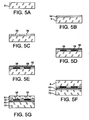
- Figure 5G shows another component according to the invention, consisting of a substrate 72 under a first buried layer 60 and a second buried layer 34 initially made of a first material, and a surface layer 61, for example made of silicon or germanium, or a III-IV or II-VI semiconductor or a semiconductor compound such as SiGe.
- This layer 61 may also be made of a piezoelectric or pyro-electric or magnetic material.
- the thickness of the layer 34 may be between 50 nm and 500 nm or 1 ⁇ m and the layer 61 may be between 10 nm and 1 ⁇ m or 50 ⁇ m thick. These thicknesses may also vary outside the ranges mentioned above.
- the second buried layer 34 comprises one or several buried areas made of a second material 56, 58 different from the first material in layer 34, the essential difference being the behaviour during a subsequent etching operation such as dry etching or wet etching; the etching rate of material 56, 58 is lower than the etching rate of the material in layer 34, which is itself greater than the etching rate of the layer 61.
- the ratio of the etching rates of the first material and the second material 56, 58 is greater than 1 or 2, or is between 2 and 10 or between 10 and 1000 and possibly even more than 1000.
- Table I above gives typical etching rates for a few materials and for some chemical etching solutions.
- the areas outside areas containing the second material 56, 58 are shown as a side view in Figure 5G . But, as illustrated in Figure 3B , their shape may be square in a plane parallel to a principal plane of the component or the layer 34, or they may have any other shape (circular, polygonal, elliptical, etc.) in the same plane. Since etching will act preferentially on the material other than material 56, 58, therefore it will be possible to make cavities of any shapes and particular square or circular or polygonal or elliptical cavities, etc.
- the second buried layer 60 is composed of the same material as the material 56, 58 or another material but also with an etching rate lower than the etching rate of the first material in the layer 34.
- etching of this first material in layer 34 will leave anchor pads of material 56, 58 and a subjacent layer 60. These pads and the layer 60 provide mechanical anchorage and stability for the surface layer 61 on the substrate 72. Therefore, these means increase the solidity of the assembly.
- a first material for example an insulating material ( Figure 5B ) for example silicon oxide (SiO 2 ) for example obtained by thermal oxidation or LPCVD or PECVD, is made on a blank silicon wafer ( Figure 5A ).
- the thickness of this layer may be about 1 ⁇ m.
- Areas 52, 54 are defined on this wafer 6 by lithography, and these areas will define the areas of future cavities ( Figure 5C ), for example by chemical etching (for example by 10% HF) or RIE etching.
- the material 34 is etched in these areas so as to completely eliminate it and to form these cavities.
- the second material 56, 58 is then deposited in these cavities ( Figure 5D ) and this material is etched at rates lower than the etching rate of the first material 34.
- This second material 56, 58 may for example be silicon nitride or polycrystalline Si if the layer 34 or the first material from which it is made is a silicon oxide SiO 2 . This second material is chosen so that it behaves differently than the first material, particularly while etching during which gases or the solution preferentially etch the silicon oxide.
- This deposition step is continued so as to leave a surface layer or film 60, that can then be levelled ( Figure 5E ), for example by mechanical - chemical polishing or using one of the levelling techniques already mentioned above.
- this film 60 may also be made of polycrystalline Si if the second material 56, 58 is already made of Si - poly.
- the material from which the layer 60 is made may be different from the material(s) 56, 58, but its etching rate will be lower than the etching rate of the first material 34.
- This wafer thus prepared is then bonded onto or is assembled with another wafer 72 that may for example be made of blank silicon ( Figure 5F ).
- a bonding layer 74 may previously have been deposited either on the substrate 72 or on the layer 60.
- two wafers can be assembled with areas defined on each.
- the two wafers can be aligned with each other.
- the result is then a structure including a "structured" buried layer 34, comprising areas filled with a first material that can be etched more easily than the second material 56, 58 and more easily than the material from which the second layer 60 is made.
- At least one of the two wafers 6, 72 may be thinned to obtain a membrane 61 ( Figure 5G ) with the required thickness, for example made of monocrystalline silicon.
- One or more wafers may be thinned by different means chosen from among-the means already mentioned as examples above.
- the component or the substrate obtained may act as an initial material for making a micro-system in layer 61, using the technique described above with reference to Figures 2A - 2D .
- the process for obtaining buried cavities is simpler than in prior art and can be used to obtain much better controlled geometries in the plane of layer 34, and particularly with any shape, circular or square or rectangular or elliptical, or any other shape defined by the lithography and etching step of layer 34.
- two cavities in the same layer may be filled with different materials, these two materials having different etching characteristics compared with the material in layer 34, and particularly their etching rates are lower than the etching rate of the layer 34.
- the pads 56, 58 that remain after the first material has been etched provide anchor pads and stability for the resulting device. If they are conducting, they may also provide electrical continuity.
Landscapes
- Engineering & Computer Science (AREA)
- Physics & Mathematics (AREA)
- Manufacturing & Machinery (AREA)
- Microelectronics & Electronic Packaging (AREA)
- Condensed Matter Physics & Semiconductors (AREA)
- General Physics & Mathematics (AREA)
- Computer Hardware Design (AREA)
- Power Engineering (AREA)
- Geometry (AREA)
- Micromachines (AREA)
- Solid-Sorbent Or Filter-Aiding Compositions (AREA)
- Laminated Bodies (AREA)
- Weting (AREA)
- Manufacture Of Macromolecular Shaped Articles (AREA)
- Silicon Polymers (AREA)
- Inorganic Insulating Materials (AREA)
Applications Claiming Priority (3)
| Application Number | Priority Date | Filing Date | Title |
|---|---|---|---|
| FR0452217A FR2875947B1 (fr) | 2004-09-30 | 2004-09-30 | Nouvelle structure pour microelectronique et microsysteme et procede de realisation |
| US67380105P | 2005-04-22 | 2005-04-22 | |
| PCT/EP2005/054854 WO2006035031A1 (en) | 2004-09-30 | 2005-09-27 | New structure for microelectronics and microsystem and manufacturing process |
Publications (2)
| Publication Number | Publication Date |
|---|---|
| EP1794789A1 EP1794789A1 (en) | 2007-06-13 |
| EP1794789B1 true EP1794789B1 (en) | 2010-12-15 |
Family
ID=34952707
Family Applications (1)
| Application Number | Title | Priority Date | Filing Date |
|---|---|---|---|
| EP05801275A Active EP1794789B1 (en) | 2004-09-30 | 2005-09-27 | Structures for microelectronics and microsystem and manufacturing process |
Country Status (9)
| Country | Link |
|---|---|
| US (2) | US20080036039A1 (ko) |
| EP (1) | EP1794789B1 (ko) |
| JP (3) | JP2008514441A (ko) |
| KR (1) | KR100860546B1 (ko) |
| CN (2) | CN102637626A (ko) |
| AT (1) | ATE492029T1 (ko) |
| DE (1) | DE602005025375D1 (ko) |
| FR (1) | FR2875947B1 (ko) |
| WO (1) | WO2006035031A1 (ko) |
Cited By (1)
| Publication number | Priority date | Publication date | Assignee | Title |
|---|---|---|---|---|
| TWI787565B (zh) * | 2018-12-20 | 2022-12-21 | 法商索泰克公司 | 用於移轉表面層至凹穴上之方法 |
Families Citing this family (18)
| Publication number | Priority date | Publication date | Assignee | Title |
|---|---|---|---|---|
| FR2876220B1 (fr) * | 2004-10-06 | 2007-09-28 | Commissariat Energie Atomique | Procede d'elaboration de structures empilees mixtes, a zones isolantes diverses et/ou zones de conduction electrique verticale localisees. |
| US20060276008A1 (en) * | 2005-06-02 | 2006-12-07 | Vesa-Pekka Lempinen | Thinning |
| FR2897982B1 (fr) * | 2006-02-27 | 2008-07-11 | Tracit Technologies Sa | Procede de fabrication des structures de type partiellement soi, comportant des zones reliant une couche superficielle et un substrat |
| FR2932923B1 (fr) | 2008-06-23 | 2011-03-25 | Commissariat Energie Atomique | Substrat heterogene comportant une couche sacrificielle et son procede de realisation. |
| FR2932788A1 (fr) | 2008-06-23 | 2009-12-25 | Commissariat Energie Atomique | Procede de fabrication d'un composant electromecanique mems / nems. |
| FR2932789B1 (fr) | 2008-06-23 | 2011-04-15 | Commissariat Energie Atomique | Procede de fabrication d'une structure electromecanique comportant au moins un pilier de renfort mecanique. |
| US7927975B2 (en) | 2009-02-04 | 2011-04-19 | Micron Technology, Inc. | Semiconductor material manufacture |
| US8637381B2 (en) * | 2011-10-17 | 2014-01-28 | International Business Machines Corporation | High-k dielectric and silicon nitride box region |
| CN104507853B (zh) | 2012-07-31 | 2016-11-23 | 索泰克公司 | 形成半导体设备的方法 |
| JPWO2014064873A1 (ja) * | 2012-10-22 | 2016-09-08 | シャープ株式会社 | 半導体装置の製造方法 |
| CN104944361B (zh) * | 2014-03-25 | 2016-05-18 | 中芯国际集成电路制造(北京)有限公司 | 一种mems器件的制作方法 |
| CN106348245B (zh) * | 2015-07-23 | 2018-02-06 | 中芯国际集成电路制造(上海)有限公司 | 一种mems器件及其制备方法、电子装置 |
| CN105895575B (zh) * | 2016-05-09 | 2018-09-25 | 中国科学院上海微系统与信息技术研究所 | 一种图形化绝缘体上硅衬底材料及其制备方法 |
| CN108190828B (zh) * | 2018-02-07 | 2024-08-13 | 北京先通康桥医药科技有限公司 | Mems传感器线阵、触诊探头及其制造方法 |
| CN108682661A (zh) * | 2018-04-17 | 2018-10-19 | 中芯集成电路(宁波)有限公司 | 一种soi基底及soi基底的形成方法 |
| FR3086096B1 (fr) | 2018-09-14 | 2021-08-27 | Soitec Silicon On Insulator | Procede de realisation d'un substrat avance pour une integration hybride |
| US10981780B2 (en) * | 2019-08-19 | 2021-04-20 | Infineon Technologies Ag | Membrane support for dual backplate transducers |
| DE102021213259A1 (de) | 2021-11-25 | 2023-05-25 | Robert Bosch Gesellschaft mit beschränkter Haftung | Verfahren zur Herstellung eines Cavity SOI Substrats und mikromechanischen Strukturen darin |
Family Cites Families (46)
| Publication number | Priority date | Publication date | Assignee | Title |
|---|---|---|---|---|
| JPS61184843A (ja) | 1985-02-13 | 1986-08-18 | Toshiba Corp | 複合半導体装置とその製造方法 |
| FR2579809B1 (fr) * | 1985-04-02 | 1987-05-15 | Thomson Csf | Procede de realisation de matrices decommande a diodes pour ecran plat de visualisation electro-optique et ecran plat realise par ce procede |
| NL8800847A (nl) * | 1988-04-05 | 1989-11-01 | Philips Nv | Werkwijze voor het vervaardigen van een halfgeleiderinrichting met een soi-struktuur. |
| US4956314A (en) * | 1989-05-30 | 1990-09-11 | Motorola, Inc. | Differential etching of silicon nitride |
| JPH088231B2 (ja) * | 1989-10-02 | 1996-01-29 | 大日本スクリーン製造株式会社 | 絶縁膜の選択的除去方法 |
| JPH0476951A (ja) * | 1990-07-18 | 1992-03-11 | Fujitsu Ltd | 半導体装置の製造方法および半導体装置 |
| US5376233A (en) * | 1992-02-10 | 1994-12-27 | Texas Instruments Incorporated | Method for selectively etching oxides |
| JP3367113B2 (ja) * | 1992-04-27 | 2003-01-14 | 株式会社デンソー | 加速度センサ |
| JPH06302834A (ja) * | 1993-04-09 | 1994-10-28 | Fujikura Ltd | 薄膜構造の製造方法 |
| US5393692A (en) * | 1993-07-28 | 1995-02-28 | Taiwan Semiconductor Manufacturing Company | Recessed side-wall poly plugged local oxidation |
| US5658698A (en) * | 1994-01-31 | 1997-08-19 | Canon Kabushiki Kaisha | Microstructure, process for manufacturing thereof and devices incorporating the same |
| JP3181174B2 (ja) * | 1994-06-08 | 2001-07-03 | キヤノン株式会社 | マイクロ構造体の形成方法 |
| US5466630A (en) * | 1994-03-21 | 1995-11-14 | United Microelectronics Corp. | Silicon-on-insulator technique with buried gap |
| JPH08105748A (ja) * | 1994-10-06 | 1996-04-23 | Murata Mfg Co Ltd | 角速度センサ、その共振周波数調整方法及びその製造方法 |
| JP3182301B2 (ja) * | 1994-11-07 | 2001-07-03 | キヤノン株式会社 | マイクロ構造体及びその形成法 |
| JP3430771B2 (ja) * | 1996-02-05 | 2003-07-28 | 株式会社デンソー | 半導体力学量センサの製造方法 |
| JPH10290036A (ja) * | 1997-04-11 | 1998-10-27 | Nissan Motor Co Ltd | 表面マイクロマシンの製造方法 |
| US6191007B1 (en) * | 1997-04-28 | 2001-02-20 | Denso Corporation | Method for manufacturing a semiconductor substrate |
| JPH1131825A (ja) * | 1997-07-10 | 1999-02-02 | Denso Corp | 半導体力学量センサの製造方法 |
| JP4144047B2 (ja) * | 1997-08-20 | 2008-09-03 | 株式会社デンソー | 半導体基板の製造方法 |
| US5976945A (en) | 1997-11-20 | 1999-11-02 | Vanguard International Semiconductor Corporation | Method for fabricating a DRAM cell structure on an SOI wafer incorporating a two dimensional trench capacitor |
| US5972758A (en) * | 1997-12-04 | 1999-10-26 | Intel Corporation | Pedestal isolated junction structure and method of manufacture |
| JP4032476B2 (ja) * | 1997-12-25 | 2008-01-16 | 日産自動車株式会社 | 微小装置の製造方法 |
| JP3424550B2 (ja) * | 1998-04-13 | 2003-07-07 | 株式会社デンソー | 半導体力学量センサの製造方法 |
| US6713235B1 (en) * | 1999-03-30 | 2004-03-30 | Citizen Watch Co., Ltd. | Method for fabricating thin-film substrate and thin-film substrate fabricated by the method |
| US6335292B1 (en) * | 1999-04-15 | 2002-01-01 | Micron Technology, Inc. | Method of controlling striations and CD loss in contact oxide etch |
| FR2795554B1 (fr) * | 1999-06-28 | 2003-08-22 | France Telecom | Procede de gravure laterale par trous pour fabriquer des dis positifs semi-conducteurs |
| WO2001006564A1 (en) * | 1999-07-15 | 2001-01-25 | Shin-Etsu Handotai Co., Ltd. | Method for producing bonded wafer and bonded wafer |
| FR2809867B1 (fr) * | 2000-05-30 | 2003-10-24 | Commissariat Energie Atomique | Substrat fragilise et procede de fabrication d'un tel substrat |
| US6372657B1 (en) * | 2000-08-31 | 2002-04-16 | Micron Technology, Inc. | Method for selective etching of oxides |
| DE10064494A1 (de) * | 2000-12-22 | 2002-07-04 | Bosch Gmbh Robert | Verfahren zur Herstellung eines Halbleiterbauelements sowie ein nach dem Verfahren hergestelltes Halbleiterbauelement, wobei das Halbleiterbauelement insbesondere eine bewegliche Masse aufweist |
| DE10124038A1 (de) * | 2001-05-16 | 2002-11-21 | Atmel Germany Gmbh | Verfahren zur Herstellung vergrabener Bereiche |
| US6835633B2 (en) * | 2002-07-24 | 2004-12-28 | International Business Machines Corporation | SOI wafers with 30-100 Å buried oxide (BOX) created by wafer bonding using 30-100 Å thin oxide as bonding layer |
| WO2004019362A1 (en) * | 2002-08-26 | 2004-03-04 | International Business Machines Corporation | Diaphragm activated micro-electromechanical switch |
| EP1396883A3 (en) * | 2002-09-04 | 2005-11-30 | Canon Kabushiki Kaisha | Substrate and manufacturing method therefor |
| FR2847077B1 (fr) * | 2002-11-12 | 2006-02-17 | Soitec Silicon On Insulator | Composants semi-conducteurs, et notamment de type soi mixtes, et procede de realisation |
| JP4007172B2 (ja) * | 2002-12-03 | 2007-11-14 | ソニー株式会社 | マイクロマシンおよびその製造方法 |
| FR2849269B1 (fr) * | 2002-12-20 | 2005-07-29 | Soitec Silicon On Insulator | Procede de realisation de cavites dans une plaque de silicium |
| DE60324960D1 (de) * | 2002-12-20 | 2009-01-08 | Soitec Silicon On Insulator | Herstellung von hohlräumen in einer siliziumscheibe |
| FR2850487B1 (fr) * | 2002-12-24 | 2005-12-09 | Commissariat Energie Atomique | Procede de realisation de substrats mixtes et structure ainsi obtenue |
| KR100546855B1 (ko) * | 2002-12-28 | 2006-01-25 | 동부아남반도체 주식회사 | 반도체 소자의 제조 방법 |
| JP4238724B2 (ja) * | 2003-03-27 | 2009-03-18 | 株式会社デンソー | 半導体装置 |
| JP2004319538A (ja) * | 2003-04-10 | 2004-11-11 | Seiko Epson Corp | 半導体装置の製造方法、集積回路、電子光学装置及び電子機器 |
| US6936491B2 (en) * | 2003-06-04 | 2005-08-30 | Robert Bosch Gmbh | Method of fabricating microelectromechanical systems and devices having trench isolated contacts |
| US6936522B2 (en) * | 2003-06-26 | 2005-08-30 | International Business Machines Corporation | Selective silicon-on-insulator isolation structure and method |
| FR2876220B1 (fr) * | 2004-10-06 | 2007-09-28 | Commissariat Energie Atomique | Procede d'elaboration de structures empilees mixtes, a zones isolantes diverses et/ou zones de conduction electrique verticale localisees. |
-
2004
- 2004-09-30 FR FR0452217A patent/FR2875947B1/fr not_active Expired - Fee Related
-
2005
- 2005-09-27 CN CN201210058695XA patent/CN102637626A/zh active Pending
- 2005-09-27 CN CNA200580033080XA patent/CN101032014A/zh active Pending
- 2005-09-27 WO PCT/EP2005/054854 patent/WO2006035031A1/en active Application Filing
- 2005-09-27 AT AT05801275T patent/ATE492029T1/de not_active IP Right Cessation
- 2005-09-27 DE DE602005025375T patent/DE602005025375D1/de active Active
- 2005-09-27 US US11/575,181 patent/US20080036039A1/en not_active Abandoned
- 2005-09-27 KR KR1020077006956A patent/KR100860546B1/ko active IP Right Grant
- 2005-09-27 EP EP05801275A patent/EP1794789B1/en active Active
- 2005-09-27 JP JP2007534016A patent/JP2008514441A/ja active Pending
-
2010
- 2010-11-30 JP JP2010266922A patent/JP2011098434A/ja active Pending
- 2010-11-30 JP JP2010266941A patent/JP2011098435A/ja active Pending
-
2012
- 2012-09-14 US US13/618,697 patent/US20130012024A1/en not_active Abandoned
Cited By (1)
| Publication number | Priority date | Publication date | Assignee | Title |
|---|---|---|---|---|
| TWI787565B (zh) * | 2018-12-20 | 2022-12-21 | 法商索泰克公司 | 用於移轉表面層至凹穴上之方法 |
Also Published As
| Publication number | Publication date |
|---|---|
| FR2875947A1 (fr) | 2006-03-31 |
| CN102637626A (zh) | 2012-08-15 |
| EP1794789A1 (en) | 2007-06-13 |
| US20080036039A1 (en) | 2008-02-14 |
| WO2006035031A1 (en) | 2006-04-06 |
| JP2008514441A (ja) | 2008-05-08 |
| KR100860546B1 (ko) | 2008-09-26 |
| JP2011098435A (ja) | 2011-05-19 |
| FR2875947B1 (fr) | 2007-09-07 |
| JP2011098434A (ja) | 2011-05-19 |
| KR20070046202A (ko) | 2007-05-02 |
| CN101032014A (zh) | 2007-09-05 |
| ATE492029T1 (de) | 2011-01-15 |
| US20130012024A1 (en) | 2013-01-10 |
| DE602005025375D1 (de) | 2011-01-27 |
Similar Documents
| Publication | Publication Date | Title |
|---|---|---|
| EP1794789B1 (en) | Structures for microelectronics and microsystem and manufacturing process | |
| US7981715B2 (en) | MEMS/NEMS structure comprising a partially monocrystalline anchor and method for manufacturing same | |
| US7456041B2 (en) | Manufacturing method of a MEMS structure, a cantilever-type MEMS structure, and a sealed fluidic channel | |
| US6620712B2 (en) | Defined sacrifical region via ion implantation for micro-opto-electro-mechanical system (MOEMS) applications | |
| US8193069B2 (en) | Stacked structure and production method thereof | |
| JP5976738B2 (ja) | マイクロテクノロジー構造を製造する方法 | |
| JP4932485B2 (ja) | 平板型構造物、特にシリコンの平板型構造物を製造する方法、前記方法の使用、及び、特にシリコンからこのようにして製造した平板型構造物 | |
| US7932118B2 (en) | Method of producing mechanical components of MEMS or NEMS structures made of monocrystalline silicon | |
| ATE511493T1 (de) | Verfahren zur herstellung von genauen mikroelektromechanischen strukturen, und so hergestellte mikrostrukturen | |
| US7399652B2 (en) | Method for manufacturing a micro-electro-mechanical device, in particular an optical microswitch, and micro-electro-mechanical device thus obtained | |
| US6413793B1 (en) | Method of forming protrusions on single crystal silicon structures built on silicon-on-insulator wafers | |
| US20050112843A1 (en) | Method for anodic bonding of wafers and device | |
| JP2976929B2 (ja) | 半導体装置の製造方法 | |
| JP4000615B2 (ja) | 微小機械の製造方法 | |
| KR20090105910A (ko) | 거친 계면을 생성하고 조절하는 방법 | |
| US20070137989A1 (en) | Optical components and production therof | |
| JPH11186566A (ja) | 微小装置の製造方法 | |
| US7094621B2 (en) | Fabrication of diaphragms and “floating” regions of single crystal semiconductor for MEMS devices | |
| Heck | Polycrystalline silicon germanium for fabrication, release, and packaging of microelectromechanical systems | |
| US6812056B2 (en) | Technique for fabricating MEMS devices having diaphragms of “floating” regions of single crystal material | |
| JP3367484B2 (ja) | 半導体装置及びその製造方法 | |
| KR100701151B1 (ko) | 미세기전집적시스템용 부양 구조물 제조 방법 | |
| KR100578259B1 (ko) | 전자장치및전자장치용막형성방법 | |
| JPH098125A (ja) | 絶縁分離基板及びその製造方法 | |
| Agarwal et al. | Controlled filling of silicon trenches with doped oxide for MEMS |
Legal Events
| Date | Code | Title | Description |
|---|---|---|---|
| PUAI | Public reference made under article 153(3) epc to a published international application that has entered the european phase |
Free format text: ORIGINAL CODE: 0009012 |
|
| 17P | Request for examination filed |
Effective date: 20070305 |
|
| AK | Designated contracting states |
Kind code of ref document: A1 Designated state(s): AT BE BG CH CY CZ DE DK EE ES FI FR GB GR HU IE IS IT LI LT LU LV MC NL PL PT RO SE SI SK TR |
|
| DAX | Request for extension of the european patent (deleted) | ||
| 17Q | First examination report despatched |
Effective date: 20090311 |
|
| RTI1 | Title (correction) |
Free format text: STRUCTURES FOR MICROELECTRONICS AND MICROSYSTEM AND MANUFACTURING PROCESS |
|
| GRAP | Despatch of communication of intention to grant a patent |
Free format text: ORIGINAL CODE: EPIDOSNIGR1 |
|
| RAP1 | Party data changed (applicant data changed or rights of an application transferred) |
Owner name: S.O.I.TEC SILICON ON INSULATOR TECHNOLOGIES |
|
| GRAS | Grant fee paid |
Free format text: ORIGINAL CODE: EPIDOSNIGR3 |
|
| GRAA | (expected) grant |
Free format text: ORIGINAL CODE: 0009210 |
|
| AK | Designated contracting states |
Kind code of ref document: B1 Designated state(s): AT BE BG CH CY CZ DE DK EE ES FI FR GB GR HU IE IS IT LI LT LU LV MC NL PL PT RO SE SI SK TR |
|
| REG | Reference to a national code |
Ref country code: GB Ref legal event code: FG4D Ref country code: CH Ref legal event code: EP |
|
| REG | Reference to a national code |
Ref country code: IE Ref legal event code: FG4D |
|
| REF | Corresponds to: |
Ref document number: 602005025375 Country of ref document: DE Date of ref document: 20110127 Kind code of ref document: P |
|
| REG | Reference to a national code |
Ref country code: NL Ref legal event code: T3 |
|
| PG25 | Lapsed in a contracting state [announced via postgrant information from national office to epo] |
Ref country code: LT Free format text: LAPSE BECAUSE OF FAILURE TO SUBMIT A TRANSLATION OF THE DESCRIPTION OR TO PAY THE FEE WITHIN THE PRESCRIBED TIME-LIMIT Effective date: 20101215 |
|
| LTIE | Lt: invalidation of european patent or patent extension |
Effective date: 20101215 |
|
| PG25 | Lapsed in a contracting state [announced via postgrant information from national office to epo] |
Ref country code: CY Free format text: LAPSE BECAUSE OF FAILURE TO SUBMIT A TRANSLATION OF THE DESCRIPTION OR TO PAY THE FEE WITHIN THE PRESCRIBED TIME-LIMIT Effective date: 20101215 Ref country code: SE Free format text: LAPSE BECAUSE OF FAILURE TO SUBMIT A TRANSLATION OF THE DESCRIPTION OR TO PAY THE FEE WITHIN THE PRESCRIBED TIME-LIMIT Effective date: 20101215 Ref country code: SI Free format text: LAPSE BECAUSE OF FAILURE TO SUBMIT A TRANSLATION OF THE DESCRIPTION OR TO PAY THE FEE WITHIN THE PRESCRIBED TIME-LIMIT Effective date: 20101215 Ref country code: BG Free format text: LAPSE BECAUSE OF FAILURE TO SUBMIT A TRANSLATION OF THE DESCRIPTION OR TO PAY THE FEE WITHIN THE PRESCRIBED TIME-LIMIT Effective date: 20110315 Ref country code: AT Free format text: LAPSE BECAUSE OF FAILURE TO SUBMIT A TRANSLATION OF THE DESCRIPTION OR TO PAY THE FEE WITHIN THE PRESCRIBED TIME-LIMIT Effective date: 20101215 Ref country code: LV Free format text: LAPSE BECAUSE OF FAILURE TO SUBMIT A TRANSLATION OF THE DESCRIPTION OR TO PAY THE FEE WITHIN THE PRESCRIBED TIME-LIMIT Effective date: 20101215 Ref country code: FI Free format text: LAPSE BECAUSE OF FAILURE TO SUBMIT A TRANSLATION OF THE DESCRIPTION OR TO PAY THE FEE WITHIN THE PRESCRIBED TIME-LIMIT Effective date: 20101215 |
|
| PG25 | Lapsed in a contracting state [announced via postgrant information from national office to epo] |
Ref country code: GR Free format text: LAPSE BECAUSE OF FAILURE TO SUBMIT A TRANSLATION OF THE DESCRIPTION OR TO PAY THE FEE WITHIN THE PRESCRIBED TIME-LIMIT Effective date: 20110316 Ref country code: CZ Free format text: LAPSE BECAUSE OF FAILURE TO SUBMIT A TRANSLATION OF THE DESCRIPTION OR TO PAY THE FEE WITHIN THE PRESCRIBED TIME-LIMIT Effective date: 20101215 Ref country code: ES Free format text: LAPSE BECAUSE OF FAILURE TO SUBMIT A TRANSLATION OF THE DESCRIPTION OR TO PAY THE FEE WITHIN THE PRESCRIBED TIME-LIMIT Effective date: 20110326 Ref country code: BE Free format text: LAPSE BECAUSE OF FAILURE TO SUBMIT A TRANSLATION OF THE DESCRIPTION OR TO PAY THE FEE WITHIN THE PRESCRIBED TIME-LIMIT Effective date: 20101215 Ref country code: IS Free format text: LAPSE BECAUSE OF FAILURE TO SUBMIT A TRANSLATION OF THE DESCRIPTION OR TO PAY THE FEE WITHIN THE PRESCRIBED TIME-LIMIT Effective date: 20110415 Ref country code: EE Free format text: LAPSE BECAUSE OF FAILURE TO SUBMIT A TRANSLATION OF THE DESCRIPTION OR TO PAY THE FEE WITHIN THE PRESCRIBED TIME-LIMIT Effective date: 20101215 Ref country code: PT Free format text: LAPSE BECAUSE OF FAILURE TO SUBMIT A TRANSLATION OF THE DESCRIPTION OR TO PAY THE FEE WITHIN THE PRESCRIBED TIME-LIMIT Effective date: 20110415 |
|
| PG25 | Lapsed in a contracting state [announced via postgrant information from national office to epo] |
Ref country code: RO Free format text: LAPSE BECAUSE OF FAILURE TO SUBMIT A TRANSLATION OF THE DESCRIPTION OR TO PAY THE FEE WITHIN THE PRESCRIBED TIME-LIMIT Effective date: 20101215 Ref country code: PL Free format text: LAPSE BECAUSE OF FAILURE TO SUBMIT A TRANSLATION OF THE DESCRIPTION OR TO PAY THE FEE WITHIN THE PRESCRIBED TIME-LIMIT Effective date: 20101215 Ref country code: SK Free format text: LAPSE BECAUSE OF FAILURE TO SUBMIT A TRANSLATION OF THE DESCRIPTION OR TO PAY THE FEE WITHIN THE PRESCRIBED TIME-LIMIT Effective date: 20101215 |
|
| PLBE | No opposition filed within time limit |
Free format text: ORIGINAL CODE: 0009261 |
|
| STAA | Information on the status of an ep patent application or granted ep patent |
Free format text: STATUS: NO OPPOSITION FILED WITHIN TIME LIMIT |
|
| PG25 | Lapsed in a contracting state [announced via postgrant information from national office to epo] |
Ref country code: DK Free format text: LAPSE BECAUSE OF FAILURE TO SUBMIT A TRANSLATION OF THE DESCRIPTION OR TO PAY THE FEE WITHIN THE PRESCRIBED TIME-LIMIT Effective date: 20101215 |
|
| 26N | No opposition filed |
Effective date: 20110916 |
|
| REG | Reference to a national code |
Ref country code: DE Ref legal event code: R097 Ref document number: 602005025375 Country of ref document: DE Effective date: 20110916 |
|
| PG25 | Lapsed in a contracting state [announced via postgrant information from national office to epo] |
Ref country code: MC Free format text: LAPSE BECAUSE OF NON-PAYMENT OF DUE FEES Effective date: 20110930 |
|
| REG | Reference to a national code |
Ref country code: CH Ref legal event code: PL |
|
| REG | Reference to a national code |
Ref country code: IE Ref legal event code: MM4A |
|
| PG25 | Lapsed in a contracting state [announced via postgrant information from national office to epo] |
Ref country code: LI Free format text: LAPSE BECAUSE OF NON-PAYMENT OF DUE FEES Effective date: 20110930 Ref country code: CH Free format text: LAPSE BECAUSE OF NON-PAYMENT OF DUE FEES Effective date: 20110930 Ref country code: IE Free format text: LAPSE BECAUSE OF NON-PAYMENT OF DUE FEES Effective date: 20110927 |
|
| REG | Reference to a national code |
Ref country code: DE Ref legal event code: R081 Ref document number: 602005025375 Country of ref document: DE Owner name: SOITEC, FR Free format text: FORMER OWNER: S.O.I.TEC SILICON ON INSULATOR TECHNOLOGIES, BERNIN, FR Effective date: 20120905 |
|
| PG25 | Lapsed in a contracting state [announced via postgrant information from national office to epo] |
Ref country code: LU Free format text: LAPSE BECAUSE OF NON-PAYMENT OF DUE FEES Effective date: 20110927 |
|
| PG25 | Lapsed in a contracting state [announced via postgrant information from national office to epo] |
Ref country code: TR Free format text: LAPSE BECAUSE OF FAILURE TO SUBMIT A TRANSLATION OF THE DESCRIPTION OR TO PAY THE FEE WITHIN THE PRESCRIBED TIME-LIMIT Effective date: 20101215 |
|
| PG25 | Lapsed in a contracting state [announced via postgrant information from national office to epo] |
Ref country code: HU Free format text: LAPSE BECAUSE OF FAILURE TO SUBMIT A TRANSLATION OF THE DESCRIPTION OR TO PAY THE FEE WITHIN THE PRESCRIBED TIME-LIMIT Effective date: 20101215 |
|
| REG | Reference to a national code |
Ref country code: FR Ref legal event code: PLFP Year of fee payment: 12 |
|
| REG | Reference to a national code |
Ref country code: FR Ref legal event code: PLFP Year of fee payment: 13 |
|
| REG | Reference to a national code |
Ref country code: FR Ref legal event code: PLFP Year of fee payment: 14 |
|
| PGFP | Annual fee paid to national office [announced via postgrant information from national office to epo] |
Ref country code: IT Payment date: 20230810 Year of fee payment: 19 |
|
| PGFP | Annual fee paid to national office [announced via postgrant information from national office to epo] |
Ref country code: NL Payment date: 20240816 Year of fee payment: 20 |
|
| PGFP | Annual fee paid to national office [announced via postgrant information from national office to epo] |
Ref country code: DE Payment date: 20240806 Year of fee payment: 20 |
|
| PGFP | Annual fee paid to national office [announced via postgrant information from national office to epo] |
Ref country code: GB Payment date: 20240808 Year of fee payment: 20 |
|
| PGFP | Annual fee paid to national office [announced via postgrant information from national office to epo] |
Ref country code: FR Payment date: 20240821 Year of fee payment: 20 |