EP1692732B1 - Electroluminescent device - Google Patents
Electroluminescent device Download PDFInfo
- Publication number
- EP1692732B1 EP1692732B1 EP04799218A EP04799218A EP1692732B1 EP 1692732 B1 EP1692732 B1 EP 1692732B1 EP 04799218 A EP04799218 A EP 04799218A EP 04799218 A EP04799218 A EP 04799218A EP 1692732 B1 EP1692732 B1 EP 1692732B1
- Authority
- EP
- European Patent Office
- Prior art keywords
- molecules
- transfer
- matrix
- quantum dots
- excitons
- Prior art date
- Legal status (The legal status is an assumption and is not a legal conclusion. Google has not performed a legal analysis and makes no representation as to the accuracy of the status listed.)
- Active
Links
- 238000012546 transfer Methods 0.000 claims abstract description 135
- 239000002096 quantum dot Substances 0.000 claims abstract description 123
- 239000011159 matrix material Substances 0.000 claims abstract description 65
- 239000011368 organic material Substances 0.000 claims abstract description 15
- 239000000243 solution Substances 0.000 claims description 29
- 238000000034 method Methods 0.000 claims description 23
- 239000000463 material Substances 0.000 claims description 21
- 230000000903 blocking effect Effects 0.000 claims description 17
- 230000005525 hole transport Effects 0.000 claims description 10
- 230000008569 process Effects 0.000 claims description 9
- 230000005281 excited state Effects 0.000 claims description 8
- 238000000151 deposition Methods 0.000 claims description 6
- 238000002156 mixing Methods 0.000 claims description 5
- 230000002542 deteriorative effect Effects 0.000 claims description 4
- 230000002708 enhancing effect Effects 0.000 claims description 4
- 239000011259 mixed solution Substances 0.000 claims description 2
- 229920000642 polymer Polymers 0.000 abstract description 47
- 239000010410 layer Substances 0.000 description 76
- MWPLVEDNUUSJAV-UHFFFAOYSA-N anthracene Chemical compound C1=CC=CC2=CC3=CC=CC=C3C=C21 MWPLVEDNUUSJAV-UHFFFAOYSA-N 0.000 description 26
- 239000000975 dye Substances 0.000 description 15
- 230000032258 transport Effects 0.000 description 13
- 238000000695 excitation spectrum Methods 0.000 description 12
- NIHNNTQXNPWCJQ-UHFFFAOYSA-N fluorene Chemical compound C1=CC=C2CC3=CC=CC=C3C2=C1 NIHNNTQXNPWCJQ-UHFFFAOYSA-N 0.000 description 12
- -1 p-phenylene vinylene Chemical group 0.000 description 11
- UHYPYGJEEGLRJD-UHFFFAOYSA-N cadmium(2+);selenium(2-) Chemical compound [Se-2].[Cd+2] UHYPYGJEEGLRJD-UHFFFAOYSA-N 0.000 description 10
- 238000004768 lowest unoccupied molecular orbital Methods 0.000 description 10
- 238000010521 absorption reaction Methods 0.000 description 9
- 238000000295 emission spectrum Methods 0.000 description 9
- 238000004770 highest occupied molecular orbital Methods 0.000 description 9
- 239000000203 mixture Substances 0.000 description 9
- 238000001228 spectrum Methods 0.000 description 9
- KAESVJOAVNADME-UHFFFAOYSA-N Pyrrole Chemical compound C=1C=CNC=1 KAESVJOAVNADME-UHFFFAOYSA-N 0.000 description 8
- YTPLMLYBLZKORZ-UHFFFAOYSA-N Thiophene Chemical compound C=1C=CSC=1 YTPLMLYBLZKORZ-UHFFFAOYSA-N 0.000 description 8
- 150000001454 anthracenes Chemical class 0.000 description 8
- 239000004065 semiconductor Substances 0.000 description 8
- 238000005259 measurement Methods 0.000 description 7
- 230000005284 excitation Effects 0.000 description 6
- 239000010408 film Substances 0.000 description 6
- 238000002347 injection Methods 0.000 description 6
- 239000007924 injection Substances 0.000 description 6
- 150000001875 compounds Chemical class 0.000 description 5
- 230000001965 increasing effect Effects 0.000 description 5
- 239000002159 nanocrystal Substances 0.000 description 5
- 125000000843 phenylene group Chemical group C1(=C(C=CC=C1)*)* 0.000 description 5
- 239000000758 substrate Substances 0.000 description 5
- APQXWKHOGQFGTB-UHFFFAOYSA-N 1-ethenyl-9h-carbazole Chemical compound C12=CC=CC=C2NC2=C1C=CC=C2C=C APQXWKHOGQFGTB-UHFFFAOYSA-N 0.000 description 4
- HEDRZPFGACZZDS-UHFFFAOYSA-N Chloroform Chemical compound ClC(Cl)Cl HEDRZPFGACZZDS-UHFFFAOYSA-N 0.000 description 4
- HSFWRNGVRCDJHI-UHFFFAOYSA-N alpha-acetylene Natural products C#C HSFWRNGVRCDJHI-UHFFFAOYSA-N 0.000 description 4
- 230000015572 biosynthetic process Effects 0.000 description 4
- 239000011258 core-shell material Substances 0.000 description 4
- 239000013078 crystal Substances 0.000 description 4
- 125000002534 ethynyl group Chemical group [H]C#C* 0.000 description 4
- 238000004519 manufacturing process Methods 0.000 description 4
- 229930192474 thiophene Natural products 0.000 description 4
- OKKJLVBELUTLKV-UHFFFAOYSA-N Methanol Chemical compound OC OKKJLVBELUTLKV-UHFFFAOYSA-N 0.000 description 3
- YXFVVABEGXRONW-UHFFFAOYSA-N Toluene Chemical compound CC1=CC=CC=C1 YXFVVABEGXRONW-UHFFFAOYSA-N 0.000 description 3
- 239000010405 anode material Substances 0.000 description 3
- 229910052788 barium Inorganic materials 0.000 description 3
- DSAJWYNOEDNPEQ-UHFFFAOYSA-N barium atom Chemical compound [Ba] DSAJWYNOEDNPEQ-UHFFFAOYSA-N 0.000 description 3
- 230000004888 barrier function Effects 0.000 description 3
- 239000010406 cathode material Substances 0.000 description 3
- 239000011162 core material Substances 0.000 description 3
- 230000003993 interaction Effects 0.000 description 3
- 229910052741 iridium Inorganic materials 0.000 description 3
- GKOZUEZYRPOHIO-UHFFFAOYSA-N iridium atom Chemical compound [Ir] GKOZUEZYRPOHIO-UHFFFAOYSA-N 0.000 description 3
- 238000004020 luminiscence type Methods 0.000 description 3
- 229910052751 metal Inorganic materials 0.000 description 3
- 239000002184 metal Substances 0.000 description 3
- 150000003057 platinum Chemical class 0.000 description 3
- 238000007639 printing Methods 0.000 description 3
- 238000005215 recombination Methods 0.000 description 3
- 230000006798 recombination Effects 0.000 description 3
- 239000011257 shell material Substances 0.000 description 3
- 238000004528 spin coating Methods 0.000 description 3
- 239000000126 substance Substances 0.000 description 3
- YLYPIBBGWLKELC-UHFFFAOYSA-N 4-(dicyanomethylene)-2-methyl-6-(4-(dimethylamino)styryl)-4H-pyran Chemical compound C1=CC(N(C)C)=CC=C1C=CC1=CC(=C(C#N)C#N)C=C(C)O1 YLYPIBBGWLKELC-UHFFFAOYSA-N 0.000 description 2
- 229910001218 Gallium arsenide Inorganic materials 0.000 description 2
- ZCQWOFVYLHDMMC-UHFFFAOYSA-N Oxazole Chemical compound C1=COC=N1 ZCQWOFVYLHDMMC-UHFFFAOYSA-N 0.000 description 2
- VYPSYNLAJGMNEJ-UHFFFAOYSA-N Silicium dioxide Chemical compound O=[Si]=O VYPSYNLAJGMNEJ-UHFFFAOYSA-N 0.000 description 2
- 230000008901 benefit Effects 0.000 description 2
- 125000004432 carbon atom Chemical group C* 0.000 description 2
- 239000003086 colorant Substances 0.000 description 2
- 239000004020 conductor Substances 0.000 description 2
- ZYGHJZDHTFUPRJ-UHFFFAOYSA-N coumarin Chemical compound C1=CC=C2OC(=O)C=CC2=C1 ZYGHJZDHTFUPRJ-UHFFFAOYSA-N 0.000 description 2
- 238000013461 design Methods 0.000 description 2
- 238000005516 engineering process Methods 0.000 description 2
- GNBHRKFJIUUOQI-UHFFFAOYSA-N fluorescein Chemical compound O1C(=O)C2=CC=CC=C2C21C1=CC=C(O)C=C1OC1=CC(O)=CC=C21 GNBHRKFJIUUOQI-UHFFFAOYSA-N 0.000 description 2
- 125000000524 functional group Chemical group 0.000 description 2
- 239000011521 glass Substances 0.000 description 2
- PQXKHYXIUOZZFA-UHFFFAOYSA-M lithium fluoride Chemical compound [Li+].[F-] PQXKHYXIUOZZFA-UHFFFAOYSA-M 0.000 description 2
- 230000007246 mechanism Effects 0.000 description 2
- 239000012044 organic layer Substances 0.000 description 2
- 150000007978 oxazole derivatives Chemical class 0.000 description 2
- 239000002245 particle Substances 0.000 description 2
- 125000002080 perylenyl group Chemical group C1(=CC=C2C=CC=C3C4=CC=CC5=CC=CC(C1=C23)=C45)* 0.000 description 2
- FIZIRKROSLGMPL-UHFFFAOYSA-N phenoxazin-1-one Chemical compound C1=CC=C2N=C3C(=O)C=CC=C3OC2=C1 FIZIRKROSLGMPL-UHFFFAOYSA-N 0.000 description 2
- IEQIEDJGQAUEQZ-UHFFFAOYSA-N phthalocyanine Chemical compound N1C(N=C2C3=CC=CC=C3C(N=C3C4=CC=CC=C4C(=N4)N3)=N2)=C(C=CC=C2)C2=C1N=C1C2=CC=CC=C2C4=N1 IEQIEDJGQAUEQZ-UHFFFAOYSA-N 0.000 description 2
- XSCHRSMBECNVNS-UHFFFAOYSA-N quinoxaline Chemical compound N1=CC=NC2=CC=CC=C21 XSCHRSMBECNVNS-UHFFFAOYSA-N 0.000 description 2
- PYWVYCXTNDRMGF-UHFFFAOYSA-N rhodamine B Chemical compound [Cl-].C=12C=CC(=[N+](CC)CC)C=C2OC2=CC(N(CC)CC)=CC=C2C=1C1=CC=CC=C1C(O)=O PYWVYCXTNDRMGF-UHFFFAOYSA-N 0.000 description 2
- 150000003384 small molecules Chemical class 0.000 description 2
- 239000002904 solvent Substances 0.000 description 2
- 230000003595 spectral effect Effects 0.000 description 2
- PJANXHGTPQOBST-UHFFFAOYSA-N stilbene Chemical compound C=1C=CC=CC=1C=CC1=CC=CC=C1 PJANXHGTPQOBST-UHFFFAOYSA-N 0.000 description 2
- 125000005504 styryl group Chemical group 0.000 description 2
- 238000006467 substitution reaction Methods 0.000 description 2
- 239000010409 thin film Substances 0.000 description 2
- OVTCUIZCVUGJHS-VQHVLOKHSA-N trans-dipyrrin Chemical compound C=1C=CNC=1/C=C1\C=CC=N1 OVTCUIZCVUGJHS-VQHVLOKHSA-N 0.000 description 2
- 150000000177 1,2,3-triazoles Chemical class 0.000 description 1
- JIHQDMXYYFUGFV-UHFFFAOYSA-N 1,3,5-triazine Chemical compound C1=NC=NC=N1 JIHQDMXYYFUGFV-UHFFFAOYSA-N 0.000 description 1
- 150000000182 1,3,5-triazines Chemical class 0.000 description 1
- UJVAZKJJYFVUKV-UHFFFAOYSA-N 1-dioctylphosphoryloctane;hexadecan-1-amine;trioctylphosphane Chemical compound CCCCCCCCCCCCCCCCN.CCCCCCCCP(CCCCCCCC)CCCCCCCC.CCCCCCCCP(=O)(CCCCCCCC)CCCCCCCC UJVAZKJJYFVUKV-UHFFFAOYSA-N 0.000 description 1
- QWENRTYMTSOGBR-UHFFFAOYSA-N 1H-1,2,3-Triazole Chemical compound C=1C=NNN=1 QWENRTYMTSOGBR-UHFFFAOYSA-N 0.000 description 1
- YMMGRPLNZPTZBS-UHFFFAOYSA-N 2,3-dihydrothieno[2,3-b][1,4]dioxine Chemical compound O1CCOC2=C1C=CS2 YMMGRPLNZPTZBS-UHFFFAOYSA-N 0.000 description 1
- BCHZICNRHXRCHY-UHFFFAOYSA-N 2h-oxazine Chemical compound N1OC=CC=C1 BCHZICNRHXRCHY-UHFFFAOYSA-N 0.000 description 1
- 229910015808 BaTe Inorganic materials 0.000 description 1
- 229910004813 CaTe Inorganic materials 0.000 description 1
- OYPRJOBELJOOCE-UHFFFAOYSA-N Calcium Chemical compound [Ca] OYPRJOBELJOOCE-UHFFFAOYSA-N 0.000 description 1
- 229910004613 CdTe Inorganic materials 0.000 description 1
- 229910004262 HgTe Inorganic materials 0.000 description 1
- 229910000673 Indium arsenide Inorganic materials 0.000 description 1
- GPXJNWSHGFTCBW-UHFFFAOYSA-N Indium phosphide Chemical compound [In]#P GPXJNWSHGFTCBW-UHFFFAOYSA-N 0.000 description 1
- 241001082241 Lythrum hyssopifolia Species 0.000 description 1
- 229910017680 MgTe Inorganic materials 0.000 description 1
- 229920000291 Poly(9,9-dioctylfluorene) Polymers 0.000 description 1
- 239000004642 Polyimide Substances 0.000 description 1
- AUNGANRZJHBGPY-SCRDCRAPSA-N Riboflavin Chemical compound OC[C@@H](O)[C@@H](O)[C@@H](O)CN1C=2C=C(C)C(C)=CC=2N=C2C1=NC(=O)NC2=O AUNGANRZJHBGPY-SCRDCRAPSA-N 0.000 description 1
- 229910004411 SrTe Inorganic materials 0.000 description 1
- PJANXHGTPQOBST-VAWYXSNFSA-N Stilbene Natural products C=1C=CC=CC=1/C=C/C1=CC=CC=C1 PJANXHGTPQOBST-VAWYXSNFSA-N 0.000 description 1
- NINIDFKCEFEMDL-UHFFFAOYSA-N Sulfur Chemical compound [S] NINIDFKCEFEMDL-UHFFFAOYSA-N 0.000 description 1
- 239000005864 Sulphur Substances 0.000 description 1
- FZWLAAWBMGSTSO-UHFFFAOYSA-N Thiazole Chemical compound C1=CSC=N1 FZWLAAWBMGSTSO-UHFFFAOYSA-N 0.000 description 1
- HCHKCACWOHOZIP-UHFFFAOYSA-N Zinc Chemical compound [Zn] HCHKCACWOHOZIP-UHFFFAOYSA-N 0.000 description 1
- 229910007709 ZnTe Inorganic materials 0.000 description 1
- 238000000862 absorption spectrum Methods 0.000 description 1
- 239000002253 acid Substances 0.000 description 1
- 150000001412 amines Chemical group 0.000 description 1
- 238000013459 approach Methods 0.000 description 1
- QVGXLLKOCUKJST-UHFFFAOYSA-N atomic oxygen Chemical compound [O] QVGXLLKOCUKJST-UHFFFAOYSA-N 0.000 description 1
- JXLHNMVSKXFWAO-UHFFFAOYSA-N azane;7-fluoro-2,1,3-benzoxadiazole-4-sulfonic acid Chemical compound N.OS(=O)(=O)C1=CC=C(F)C2=NON=C12 JXLHNMVSKXFWAO-UHFFFAOYSA-N 0.000 description 1
- RLECCBFNWDXKPK-UHFFFAOYSA-N bis(trimethylsilyl)sulfide Chemical compound C[Si](C)(C)S[Si](C)(C)C RLECCBFNWDXKPK-UHFFFAOYSA-N 0.000 description 1
- 239000013590 bulk material Substances 0.000 description 1
- VQNPSCRXHSIJTH-UHFFFAOYSA-N cadmium(2+);carbanide Chemical compound [CH3-].[CH3-].[Cd+2] VQNPSCRXHSIJTH-UHFFFAOYSA-N 0.000 description 1
- 229910052791 calcium Inorganic materials 0.000 description 1
- 239000011575 calcium Substances 0.000 description 1
- 150000007942 carboxylates Chemical class 0.000 description 1
- 238000005229 chemical vapour deposition Methods 0.000 description 1
- 239000011248 coating agent Substances 0.000 description 1
- 238000000576 coating method Methods 0.000 description 1
- 239000002131 composite material Substances 0.000 description 1
- 239000002322 conducting polymer Substances 0.000 description 1
- 229920001940 conductive polymer Polymers 0.000 description 1
- 229920001577 copolymer Polymers 0.000 description 1
- 238000012937 correction Methods 0.000 description 1
- 230000008878 coupling Effects 0.000 description 1
- 238000010168 coupling process Methods 0.000 description 1
- 238000005859 coupling reaction Methods 0.000 description 1
- 230000007423 decrease Effects 0.000 description 1
- 239000000412 dendrimer Substances 0.000 description 1
- 229920000736 dendritic polymer Polymers 0.000 description 1
- 230000008021 deposition Effects 0.000 description 1
- AXAZMDOAUQTMOW-UHFFFAOYSA-N dimethylzinc Chemical compound C[Zn]C AXAZMDOAUQTMOW-UHFFFAOYSA-N 0.000 description 1
- 238000004090 dissolution Methods 0.000 description 1
- 238000009826 distribution Methods 0.000 description 1
- 230000005684 electric field Effects 0.000 description 1
- 238000005538 encapsulation Methods 0.000 description 1
- 150000002211 flavins Chemical class 0.000 description 1
- 239000012530 fluid Substances 0.000 description 1
- 150000002220 fluorenes Chemical class 0.000 description 1
- 238000009472 formulation Methods 0.000 description 1
- 239000003292 glue Substances 0.000 description 1
- 150000002430 hydrocarbons Chemical group 0.000 description 1
- WPYVAWXEWQSOGY-UHFFFAOYSA-N indium antimonide Chemical compound [Sb]#[In] WPYVAWXEWQSOGY-UHFFFAOYSA-N 0.000 description 1
- RPQDHPTXJYYUPQ-UHFFFAOYSA-N indium arsenide Chemical compound [In]#[As] RPQDHPTXJYYUPQ-UHFFFAOYSA-N 0.000 description 1
- AMGQUBHHOARCQH-UHFFFAOYSA-N indium;oxotin Chemical compound [In].[Sn]=O AMGQUBHHOARCQH-UHFFFAOYSA-N 0.000 description 1
- ZLTPDFXIESTBQG-UHFFFAOYSA-N isothiazole Chemical compound C=1C=NSC=1 ZLTPDFXIESTBQG-UHFFFAOYSA-N 0.000 description 1
- 150000003854 isothiazoles Chemical class 0.000 description 1
- CTAPFRYPJLPFDF-UHFFFAOYSA-N isoxazole Chemical compound C=1C=NOC=1 CTAPFRYPJLPFDF-UHFFFAOYSA-N 0.000 description 1
- 150000002545 isoxazoles Chemical class 0.000 description 1
- 239000006193 liquid solution Substances 0.000 description 1
- 230000005012 migration Effects 0.000 description 1
- 238000013508 migration Methods 0.000 description 1
- 238000004776 molecular orbital Methods 0.000 description 1
- 239000002105 nanoparticle Substances 0.000 description 1
- 239000012454 non-polar solvent Substances 0.000 description 1
- WCPAKWJPBJAGKN-UHFFFAOYSA-N oxadiazole Chemical compound C1=CON=N1 WCPAKWJPBJAGKN-UHFFFAOYSA-N 0.000 description 1
- 150000004866 oxadiazoles Chemical class 0.000 description 1
- 150000004893 oxazines Chemical class 0.000 description 1
- 239000001301 oxygen Substances 0.000 description 1
- 229910052760 oxygen Inorganic materials 0.000 description 1
- 238000002161 passivation Methods 0.000 description 1
- CSHWQDPOILHKBI-UHFFFAOYSA-N peryrene Natural products C1=CC(C2=CC=CC=3C2=C2C=CC=3)=C3C2=CC=CC3=C1 CSHWQDPOILHKBI-UHFFFAOYSA-N 0.000 description 1
- UOMHBFAJZRZNQD-UHFFFAOYSA-N phenoxazone Natural products C1=CC=C2OC3=CC(=O)C=CC3=NC2=C1 UOMHBFAJZRZNQD-UHFFFAOYSA-N 0.000 description 1
- UEZVMMHDMIWARA-UHFFFAOYSA-M phosphonate Chemical compound [O-]P(=O)=O UEZVMMHDMIWARA-UHFFFAOYSA-M 0.000 description 1
- 238000005424 photoluminescence Methods 0.000 description 1
- 238000005240 physical vapour deposition Methods 0.000 description 1
- 239000004033 plastic Substances 0.000 description 1
- 229920000767 polyaniline Polymers 0.000 description 1
- 229910021420 polycrystalline silicon Inorganic materials 0.000 description 1
- 229920001721 polyimide Polymers 0.000 description 1
- 229920005591 polysilicon Polymers 0.000 description 1
- 238000005381 potential energy Methods 0.000 description 1
- 238000001556 precipitation Methods 0.000 description 1
- 239000002243 precursor Substances 0.000 description 1
- 238000002360 preparation method Methods 0.000 description 1
- 238000006862 quantum yield reaction Methods 0.000 description 1
- 238000010791 quenching Methods 0.000 description 1
- 230000000171 quenching effect Effects 0.000 description 1
- 150000003252 quinoxalines Chemical class 0.000 description 1
- 229910052761 rare earth metal Inorganic materials 0.000 description 1
- SBIBMFFZSBJNJF-UHFFFAOYSA-N selenium;zinc Chemical compound [Se]=[Zn] SBIBMFFZSBJNJF-UHFFFAOYSA-N 0.000 description 1
- 239000004054 semiconductor nanocrystal Substances 0.000 description 1
- 229910052710 silicon Inorganic materials 0.000 description 1
- 239000000377 silicon dioxide Substances 0.000 description 1
- 230000003019 stabilising effect Effects 0.000 description 1
- 235000021286 stilbenes Nutrition 0.000 description 1
- 238000003786 synthesis reaction Methods 0.000 description 1
- 150000003513 tertiary aromatic amines Chemical class 0.000 description 1
- VLLMWSRANPNYQX-UHFFFAOYSA-N thiadiazole Chemical compound C1=CSN=N1.C1=CSN=N1 VLLMWSRANPNYQX-UHFFFAOYSA-N 0.000 description 1
- 150000004867 thiadiazoles Chemical class 0.000 description 1
- 150000007979 thiazole derivatives Chemical class 0.000 description 1
- 125000003396 thiol group Chemical group [H]S* 0.000 description 1
- 230000007704 transition Effects 0.000 description 1
- 229910052723 transition metal Inorganic materials 0.000 description 1
- ZAKSIRCIOXDVPT-UHFFFAOYSA-N trioctyl(selanylidene)-$l^{5}-phosphane Chemical compound CCCCCCCCP(=[Se])(CCCCCCCC)CCCCCCCC ZAKSIRCIOXDVPT-UHFFFAOYSA-N 0.000 description 1
- XLYOFNOQVPJJNP-UHFFFAOYSA-N water Substances O XLYOFNOQVPJJNP-UHFFFAOYSA-N 0.000 description 1
- 238000007704 wet chemistry method Methods 0.000 description 1
- 229910052725 zinc Inorganic materials 0.000 description 1
- 239000011701 zinc Substances 0.000 description 1
Images


Classifications
-
- H—ELECTRICITY
- H05—ELECTRIC TECHNIQUES NOT OTHERWISE PROVIDED FOR
- H05B—ELECTRIC HEATING; ELECTRIC LIGHT SOURCES NOT OTHERWISE PROVIDED FOR; CIRCUIT ARRANGEMENTS FOR ELECTRIC LIGHT SOURCES, IN GENERAL
- H05B33/00—Electroluminescent light sources
- H05B33/12—Light sources with substantially two-dimensional radiating surfaces
- H05B33/14—Light sources with substantially two-dimensional radiating surfaces characterised by the chemical or physical composition or the arrangement of the electroluminescent material, or by the simultaneous addition of the electroluminescent material in or onto the light source
-
- B—PERFORMING OPERATIONS; TRANSPORTING
- B82—NANOTECHNOLOGY
- B82Y—SPECIFIC USES OR APPLICATIONS OF NANOSTRUCTURES; MEASUREMENT OR ANALYSIS OF NANOSTRUCTURES; MANUFACTURE OR TREATMENT OF NANOSTRUCTURES
- B82Y10/00—Nanotechnology for information processing, storage or transmission, e.g. quantum computing or single electron logic
-
- B—PERFORMING OPERATIONS; TRANSPORTING
- B82—NANOTECHNOLOGY
- B82Y—SPECIFIC USES OR APPLICATIONS OF NANOSTRUCTURES; MEASUREMENT OR ANALYSIS OF NANOSTRUCTURES; MANUFACTURE OR TREATMENT OF NANOSTRUCTURES
- B82Y20/00—Nanooptics, e.g. quantum optics or photonic crystals
-
- B—PERFORMING OPERATIONS; TRANSPORTING
- B82—NANOTECHNOLOGY
- B82Y—SPECIFIC USES OR APPLICATIONS OF NANOSTRUCTURES; MEASUREMENT OR ANALYSIS OF NANOSTRUCTURES; MANUFACTURE OR TREATMENT OF NANOSTRUCTURES
- B82Y30/00—Nanotechnology for materials or surface science, e.g. nanocomposites
-
- H—ELECTRICITY
- H10—SEMICONDUCTOR DEVICES; ELECTRIC SOLID-STATE DEVICES NOT OTHERWISE PROVIDED FOR
- H10K—ORGANIC ELECTRIC SOLID-STATE DEVICES
- H10K50/00—Organic light-emitting devices
- H10K50/10—OLEDs or polymer light-emitting diodes [PLED]
- H10K50/11—OLEDs or polymer light-emitting diodes [PLED] characterised by the electroluminescent [EL] layers
- H10K50/115—OLEDs or polymer light-emitting diodes [PLED] characterised by the electroluminescent [EL] layers comprising active inorganic nanostructures, e.g. luminescent quantum dots
-
- H—ELECTRICITY
- H10—SEMICONDUCTOR DEVICES; ELECTRIC SOLID-STATE DEVICES NOT OTHERWISE PROVIDED FOR
- H10K—ORGANIC ELECTRIC SOLID-STATE DEVICES
- H10K2101/00—Properties of the organic materials covered by group H10K85/00
- H10K2101/10—Triplet emission
-
- H—ELECTRICITY
- H10—SEMICONDUCTOR DEVICES; ELECTRIC SOLID-STATE DEVICES NOT OTHERWISE PROVIDED FOR
- H10K—ORGANIC ELECTRIC SOLID-STATE DEVICES
- H10K59/00—Integrated devices, or assemblies of multiple devices, comprising at least one organic light-emitting element covered by group H10K50/00
- H10K59/30—Devices specially adapted for multicolour light emission
- H10K59/35—Devices specially adapted for multicolour light emission comprising red-green-blue [RGB] subpixels
Definitions
- Organic electroluminescent devices are considered to be important in many applications ranging from lighting to full colour emissive displays.
- the basic structure is an emitting organic layer sandwiched between electrode layers and transport layers providing electrons and holes to the emitting layer.
- Organic light emitting materials can be engineered to show both good electron as well as good hole transport.
- the HOMO and LUMO levels of electroluminescent polymers can be adjusted so that they can be used with commonly available cathode and anode materials (e.g., ITO anode, barium cathode).
- cathode and anode materials e.g., ITO anode, barium cathode.
- anode materials e.g., ITO anode, barium cathode.
- Small organic molecules are also used in the production of electroluminescent devices, OLEDs. In the case of OLEDs usually more than three layers are used in order to improve the efficiency of the devices.
- quantum dots nano-sized semiconductor crystals referred to as quantum dots (QDs) have been proposed as a substitution for dyes in OLEDs and PolyLEDs.
- QDs quantum dots
- organic host material such as a layered structure
- QD-OLED or PolyLED Such devices are described in e.g. " Quantum dot leap", The Engineer (ISSN 0013-7758) 291, 19, 2002 and "Quantum-dot composite LED emits in IR”, Photonics Technology World, June 2003 (http:/www.photonics.com/spectra/tech/XQ/ASP/techid.1557/QX/read.htm).
- QD Electrons and holes injected into the matrix create excitons in the polymers, which are transferred to the QDs for recombination and light emission.
- QD provides a number of advantages over dyes. Although reactive, it is relatively easy to encapsulate QD in a "passivation” or “capping", layer for making them resistant to air and humidity.
- QDs have the unique property of emitting light at a frequency determined by their size. Thus, the emission wavelength from QDs can be precisely and continuously tuned over a large span of wavelengths simply by adjusting their size during fabrication.
- QDs As compared with dyes is more difficult.
- Delocalised ⁇ molecular orbitals in conjugated hydrocarbon chains in the organic molecules and in polymers provide efficient transportation of electrons, holes and excitons.
- the injection of holes and electrons creates excitons at random locations within the emitting layer, often far away from the QD.
- electrons and holes may be transported in the organic host material and recombine at the QDs without proper exciton formation.
- the good electron and hole transport allows for the creation and transport of excitons in the layer, but the coupling of excitons from the electroluminescent material into the QDs presents a bottleneck.
- QD-OLEDs or PolyLEDs are not to be confused with other types of LEDs featuring QDs, where a thin layer of QDs are sandwiched between organic semiconductor (hole and electron) transportation layers.
- electrons and holes are supplied directly to the QDs or the capping molecules on the QDs, not in an organic host material, and hole/electron and exciton transport or decay is not an issue.
- WO 03/021694 describes an electroluminescent device wherein the device is characterized by a light emitting layer comprising quantum dots.
- the quantum dots are provided with capping molecules with functional units on the quantum dot surfaces which cause excited state injection into the quantum dots.
- the capping molecules with functional units comprise exciton transport moieties, which cause the injection of excitons to the core of the quantum dots.
- WO 03/084292 describes an electrically pumped light emitting devices including nanocrystals (or quantum dots) as the electroluminescent material.
- the described light emitting device includes a first electrode, a layer including a in a matrix, a first electrode, a second electrode opposed to the first electrode and a plurality of semiconductor nanocrystals disposed between the first electrode and the second electrode.
- the matrix can be non-polymeric, for example, a small molecule.
- the invention provides a method for improving electrical energy transfer from electroluminescent organic molecules to quantum dots embedded in an organic material matrix, the method comprising the steps of
- the embedding of QDs in the matrix means that the QD are spatially distributed throughout the organic matrix.
- the QDs are preferably at least substantially homogeneously distributed in the organic matrix.
- the spatial distribution may be random or ordered, or anything in between.
- the QDs are preferably bound or in close contact to the organic molecules by some at least substantially bond-like interaction.
- the QDs are embedded in the organic host material, and therefore form a single, QD-doped, emissive layer.
- a matrix of electroluminescent organic molecules, preferably polymers, with embedded QDs is typically formed by blending or mixing liquid solutions of organic molecules and the QDs.
- the resulting solution may be deposited on a substrate, typically by spin-coating, such as an electrode and allowed to dry out, thereby forming the matrix.
- Transfer molecules will typically be provided on the surfaces of the QDs before the QD solution is mixed into the organic solution.
- the electroluminescent organic molecules may be any of the electroluminescent organic substances presently used in OLEDs and PolyLEDs. However, in order to form a suitable organic matrix, the substance is preferably soluble or can be modified to be soluble. This allows for the proper embedding of the QDs in the organic matrix. A further advantage of such substances is that they can be processed from solution, so that the emissive layer can be readily patterned for multi- or full colour emission. Further, the organic host material and QD solution may only be partially dried out, so that a fluid emissive layer may be formed.
- the electroluminescent organic molecules according to the invention are electroluminescent polymers.
- Polymers are organic molecules, and both “organic molecules” and “polymers” will be used to designate the matrix host material of the light emitting layer in the following description, without the intention of limiting the scope to polymers only.
- the lifetime of excited states or excitons in the electroluminescent organic molecules is not long enough for the exciton transfer to the QDs to take place. While excited states directly on the surface of the quantum dots show almost 100% energy transfer, this value reduces to about 10% already at a distance of 3nm from the surface of the quantum dots. Because of this behavior the excitons need to be brought to a closer proximity to the quantum dots in order to increase the energy transfer rate. This can be achieved by placing an exciton recombination and/or transfer molecule on the surface of the quantum dot. However it is still necessary to transfer the excited state created in the organic matrix to the transfer molecule.
- n 9.78 10 3
- Q D the donor fluorescence quantum yield in the absence of the acceptor
- J( ⁇ ) is a spectral overlap integral (in M -1 ⁇ cm 3 ).
- k 2 is a geometric factor, which averages out to 2/3 in the case of freely rotating dyes.
- k ET is the rate of energy transfer from the organic molecule to the energy transfer molecule and k R and k NR are the radiative and nonradiative rate of the donor, respectively.
- This equation suggests that energy transfer is efficient if k ET > k R + k NR . While the Förster energy transfer between singlet excitons takes place in the nanosecond time scale, the triplet-triplet Dexter energy transfer is often in the microsecond range. Therefore the exciton lifetime must be longer than the microsecond range to have an efficient triplet-triplet energy transfer by the Dexter mechanism.
- a transfer molecule is a molecule capable of receiving an exciton from an organic molecule, preferably a polymer of the matrix and transfer an exciton to the QD.
- a transfer molecule is a molecule which can be excited by an excited state in an organic molecule of the matrix, e.g. by exchange interaction (Dexter energy transfer) or by more long-range dipolar interactions (Förster energy transfer), and which excited transfer molecule can excite the QD by a similar mechanism.
- a transfer molecule is selected to have a bandgap, E transfer , which is smaller than a bandgap, E org. mol. , of the electroluminescent molecules of the matrix and larger than a bandgap, E QD , of the quantum dots.
- E transfer a bandgap
- E QD a bandgap
- a transfer molecule is preferably selected so that a transfer rate of excitons from the electroluminescent organic molecules s to the transfer molecules is larger than the decay rate of excitons in the electroluminescent host.
- a transfer molecule is preferably selected so that a transfer rate of excitons from the transfer molecules to the quantum dots is larger than a decay rate of excitons in the transfer molecules.
- a transfer molecule is a phosphorescing molecule having excitable long lived excited triplet states, i.e. excitons will have small decay/recombination rates.
- the transfer molecules can be chosen so that they have a minimal distance to the QD and to the electroluminescent organic host molecules.
- the two-step energy transfer process makes it possible to reduce - indirectly - the effective distance between the QD and the organic molecules. Care should be taken to avoid too many of these molecules are present on the surface, so that concentration quenching is avoided.
- the invention provides a quantum dot embedded organic material device with improved electrical energy transfer from electroluminescent organic molecules to embedded quantum dots, the device comprising
- the one or more transfer molecules are preferably chosen so that a transfer rate of excitons from the transfer molecules to the quantum dots is larger than a decay rate of excitons in the transfer molecules.
- the device according to the second aspect is a light emitting device, i.e. a QD-PolyLED.
- a light emitting device i.e. a QD-PolyLED.
- a layered structure can be produced where the excitons are first created on the polymer, subsequently transferred to surface modifying molecules, and finally to the quantum dot where the emission takes place.
- the HOMO and LUMO levels of electroluminescent polymers can be adjusted, so that they can be used with commonly available cathode and anode materials, such as an ITO anode and a barium cathode, so as to form a three layer structure.
- the light emitting device comprises one or more further layers such as a hole transporting and electron blocking layer and/or a electron transporting and hole blocking layer in addition to the organic emitting layer.
- Such layers located between the respective electrodes and the organic matrix, serves to provide efficient hole/electron transport from the cathode/anode into the light emitting layer, while confining the excitons in the emitting layer
- the electron transport (hole blocking) layer is placed at the cathode side and would have a LUMO level which is the same as that of the organic matrix and a HOMO level preferably lower than that of the organic matrix.
- Such a material is also expected to show much higher electron mobility than hole mobility.
- the ideal hole transport (electron blocking) layer is placed at the anode side on the other hand would have a LUMO level which is higher than that of the organic matrix and a HOMO level preferably slightly lower than that of the organic matrix while being higher than the fermi level of the anode.
- Such a hole transport (electron blocking) layer is also expected to show much higher hole mobility than electron mobility.
- the method according to the first aspect of the invention may comprise the step of confining electrons and holes in the matrix by providing electron and hole blocking layers adjacent to the matrix.
- the invention may be applied in a display comprising a plurality of pixels, each pixel comprising a light emitting quantum dot embedded organic molecule device according to the second aspect of the invention.
- the display is active in that an on/off state of each pixel can be controlled individually.
- the display is a colour display in that the pixels have different colours, such as two or more different colours, e.g. red, green and blue. The colour of a pixel is determined by the bandgap, and thereby the size, of the quantum dots embedded in the light emitting layer of the pixel.
- the invention provides a process for fabricating a light emitting quantum dot embedded organic device with improved electrical energy transfer from electroluminescent organic molecules to quantum dots, the process comprising the steps of:
- the process further comprises one or more of the following steps:
- the principle behind the above aspects of the invention is to use a two-step energy transfer process to improve electrical energy transfer from electroluminescent organic molecule s to quantum dots embedded therein. It is clear from the above that the nonradiative energy transfer is inversely proportional with the distance between the emitting centres, the efficiency of the exciton transfer to the QDs decreases non-linearly with increasing distance. By introducing an intermediate stage, the transfer molecule attached to the QD, two shorter transitions is obtained instead of one long. The overall efficiency is then improved due to the non-linear dependence of the energy transfer on distance.
- the invention may be applied to improve the power efficiency and performance of all devices based on an electroluminescent organic matrix with embedded QDs.
- the invention may thus lead to the use of such devices in a large number of applications where other light emitting devices are presently used. Also, it may lead to the use of such devices in areas into which the present efficiency of electrical energy transfer have impeded the possibility of migration of this technology.
- the invention is not restricted to improve light emitting devices, but may be used to improve the power efficiency and performance of devices based on an organic matrix with embedded QDs in other areas, such as micro/nanoelectronic components, sensors, photovoltaic devices, and other non-emissive devices.
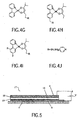
- the invention provides a light emitting device 2.
- the device comprises a cathode 4 and a transparent anode 6 on a transparent substrate 5 with a power supply 8 for creating an electrical field between these.
- a light emitting layer 10 consisting of a blend of electroluminescent organic molecules and QDs.
- the organic molecules are polymers.
- FIG 2 shows an illustration of an enlarged section of the device 2 of Figure 1 , the figure exaggerates the relative size.
- the light emitting layer 10 is seen to consist of a matrix of polymers 12 with QDs 14 with transfer molecules distributed throughout the matrix.
- a thin film planarising layer 11 is seen between the anode 6 and the light emitting layer 10.
- the electrode work functions should match the HOMO and LUMO levels in the polymer so that it is easy to inject a steady supply of electron and hole pairs into the polymer.
- a thin layer of transparent conductor indium tin oxide (ITO) is deposited on the glass or plastic substrate 5.
- a thin film planarising layer 11, typically 50 to 150-nm thick, is deposited on the anode 6 from solution using e.g. spin coating or a printing technique.
- the planarising layer is a non-emissive conducting polymer, poly-ethylenedioxythiophene (PEDOT) or polyaniline doped with poly-styrenesulphonic acid (PSS), which serves as a hole-injecting layer and has an even higher work function than ITO.
- PEDOT poly-ethylenedioxythiophene
- PSS poly-styrenesulphonic acid
- a metallic cathode 4 is evaporated on top of the emissive layer 10.
- the cathode 4 is a reflective metal layer with a low work function to match the LUMO level of the polymer-for example, calcium or barium. Alternative fabrication techniques and structures are possible.
- the difference in work function between the cathode and anode materials is typically less than the polymer bandgap.
- an energy barrier preventing the electrons and holes entering the polymer, which impairs exciton generation, reducing efficiency.
- This potential energy barrier to charge injection is usually present at the cathode/polymer interface.
- One solution to this problem is to insert a thin layer of dielectric, such as lithium fluoride, at the cathode, which enhances electron injection and improves device efficiency.
- the device is typically hermetically sealed to prevent the ingress of water and oxygen that can degrade the organic materials and the reactive metal cathode.
- Present-generation structures typically use a metal or glass can encapsulation, with a glue seal to the substrate.
- the organic matrix forming the light emitting layer is formed when a mixture of organic molecules and QD solutions are deposited and the solvent evaporated.
- Typical electroluminescent polymers and oligomers are poly- or oligo p-phenylene vinylene (PPV) and the poly- or oligofluorene family (e.g. poly(9,9'-dioctylfluorene)).
- Other electroluminescent polymers comprise poly- or oligo-phenylenes, poly- or oligo-phenylethylenes, poly- or oligo-indenofluorenes, poly- or oligo-vinylcarbazoles, poly- or oligo-oxadiazoles, and copolymers or blends thereof.
- small organic molecules with suitable side groups for solubility and film forming. They can also be in the form of highly branched molecules such as dendrimers in order to improve their solubility as well as film forming properties.
- small molecules are a fluorene, a fluorene derivative, a perylene, a perylene derivative, a coumarine, a coumarine derivative, a phenoxazone, a phenoxazone derivative, 4-dicyanmethylene-2-methyl-6- (p-dimethylaminostyryl)-4H-pyran (DCM), a 4-dicyanmethylene-2-methyl-6-(p-dimethylaminostyryl)-4H-pyran derivative, a rhodamine, a rhodamine derivative, an oxazine, an oxazine derivative, an oxazole, an oxazole derivative, a styryl, a styryl
- Triplet emitters based in Iridium, and platinum complexes can also be used. These systems may also contain electron and/or hole conducting moieties listed below in order to improve charge transport within them. It is possible to tune the electrical properties of band gap, electron affinity, and charge transport, and rheological properties such as viscosity and solubility by various substitutions, thus tailoring the material to the specific application and deposition method.
- a QD 14 with transfer molecules 15 is shown in Figure 3 .
- the QDs are preferably prepared by wet chemical processes, and transfer molecules 15 are added to the surface after formation of the QD.
- QDs are semiconductor nanometer crystals and may comprise Group [II-VI] semiconductor compounds such as MgS, MgSe, MgTe, CaS, CaSe, CaTe, SrS, SrSe, SrTe, BaS, BaSe, BaTe, ZnS, ZnSe, ZnTe, CdS, CdSe, CdTe, HgS, HgSe and HgTe; and/or crystals of Group [III-V] semiconductor compounds such as GaAs, GaP, InN, InAs, InP and InSb; and/or crystals of group IV semiconductor compounds such as Si and Ge.
- Group [II-VI] semiconductor compounds such as MgS, MgSe, MgTe, CaS, CaSe, CaTe
- the semiconductor compounds may be doped with rare earth metal cations or transition metal cations such as Eu 3+ , Tb 3+ , Mn 2+ , Ag + or Cu + .
- a QD consists of two ore more semiconductor compounds. Most likely the QDs comprise InN, InGaP or GaAs. The radii of the QDs are smaller than the exciton Bohr radius of the respective bulk material. Most likely the QDs have radii no larger than about 10 nm.
- the QDs comprise a core-shell structure.
- a QD consists of light emitting core material, e.g. CdSe overcoated with a shell material of higher bandgap, e.g. ZnS, such that an exciton is confined to the core of the QD.
- Colloidal luminescent CdSe/ZnS core-shell nanocrystals can be synthesized via two-stage approach.
- the monodisperse CdSe nanocrystals are prepared by reacting dimethylcadmium with trioctylphosphine selenide in hexadecylamine - trioctylphosphine oxide - trioctylphosphine (HDA-TOPO-TOP) stabilising mixture at 270-310°C.
- the ZnS shell around the colloidal CdSe cores are grown by slow addition of dimethylzinc and bis-trimethylsilylsulfide (zinc and sulphur precursors correspondingly) into the solution of CdSe cores in HDA-TOPO-TOP mixture at 180-220°C.
- the resulting CdSe/ZnS core-shell nanocrystals have a HDA-TOPO-TOP surface coating and are soluble in non-polar solvents like chloroform or toluene.
- Core-shell CdSe/ZnS nanocrystals exhibit strong band-edge photoluminescence with room temperature quantum efficiencies as high as 30-70%.
- the spectral position of the emission band is tuneable from blue to red with increasing the size of CdSe core from ⁇ 2 to 6 nm Thin ( ⁇ 2 monolayers) ZnS epitaxial shell grown around CdSe core considerably improves particle stability and the luminescence efficiency.
- the surface of the particles can be modified using other molecule resulting in total or partial replacement of HDA-TOPO-TOP.
- they can be subjected to standard capping exchange procedure.
- An excess amount of transfer molecules with suitable functional groups are added to the QD solution in chloroform and stirred at 50 °C for several hours.
- Methanol can be used to precipitate the QDs. The dissolution and precipitation steps are repeated several times in order to remove transfer molecules which were not bound to QD surfaces.
- the transfer molecules can be chosen to have a small distance to the QD by introduction of a functional group which attaches directly to the surface of the QD, e.g., through a carboxylate, phosphonate, sulphonate or thiol-group.
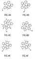
- triplet emitters based in Iridium, and platinum complexes such as those shown in Figures 4A-J can be applied as transfer molecules.
- FIG. 5 shows a device 17 similar to the device 2 in Figure 1 with such layers. Between cathode 4 and organic matrix 10, a hole transporting and electron blocking layer 19 is formed. Similarly, an electron transporting and hole blocking layer 18 is formed between anode 6 and organic matrix 10.
- Hole transporting, electron bloeking material layer 19 may comprise a tertiary aromatic amine, a thiophene oligomer, a thiophene polymer, a pyrrol oligomer, a pyrrol polymer, a phenylenevinylene oligomer, a phenylenevinylene polymer, a vinylcarbazol oligomer, a vinylcarbazol polymer, a fluorene oligomer, a fluorene polymer, a phenylenethyne oligomer, a phenylenethyne polymer, a phenylene oligomer, a phenylene polymer, an acetylene oligomer, an acetylene polymer, a phthalocyanine, a phthalocyanine derivative, a porphyrine or a porphyrine derivative.
- One or more carbon atoms of the oligomers or polymers may also be substituted.
- a material layer may also comprise molecules with a functional unit such as a triphehyl amine unit, a phenylenevinylene oligomer unit, a phenylene oligomer unit or a fluorene oligomer unit.
- dyes having the highest occupied molecular orbital (HOMO) within the range of about four and about six eV can be used as hole transporting, electron blocking material layer 19.
- Electron transporting, hole blocking material layer 18 may comprise an oxadiazole, an oxadiazole derivative, an oxazole, an oxazole derivative, an isoxazole, an isoxazole derivative, a thiazole, a thiazole derivative, an isothiazole, an isothiazole derivative, a thiadiazole, a thiadiazole derivative, a 1,2, 3 triazole, a 1,2,3 triazole derivative, a 1,3,5 triazine, a 1,3, 5 triazine derivative, a quinoxaline, a quinoxaline derivative, a pyrrol oligomer, a pyrrol polymer, a phenylenevinylene oligomer, a phenylenevinylene polymer, a vinylcarbazol oligomer, a vinylcarbazol polymer, a fluorene oligomer, a fluorene polymer, a phenylenethyn
- the electron transport (hole blocking) layer needs to have a LUMO which is almost the same as that of the host organic material where the QDs are buried while the hole transport (electron blocking) layer needs to have a LUMO which is almost the same as that of the host organic material.
- hole and electron transport layers that the band gap is in the order of 6eV. These layers can be deposited from a solution, by physical or chemical vapour deposition. When solution deposition is used it is necessary to use a solvent which will not dissolve the layers
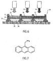
- the invention is used to form a plurality of light emitting devices forming a pixel array in an active colour display.
- Figure 6 shows a standard colour display design 20 which can be used to form a colour display using the highly efficient organic matrix with embedded QDs according to the present invention.
- a pattern of individual red, green and blue pixels are formed, typically by printing the organic and QD mixture solutions 22, 23 and 24 directly into pre-patterned wells.
- Three different organic material and QD mixture solutions 22, 23 and 24 are needed, each having the QD-size tuned to create emission at an appropriate red, green or blue wavelength.
- Each pixel corresponds to the device 2 described in relation to Figure 1 .
- a transparent anode 28 is formed on top of a polysilicon TFT substrate 30 forms the bottom of the well, while a polyimide layer 31 on top of an insulating silica separator 32 forms the barriers.
- a planarising and hole-injecting PEDOT layer 34 is deposited on the anode 28. When the solute of the organic material and QD mixture solutions 22, 23 and 24 evaporate, the organic matrices 35, 36 and 37 with red, green and blue light emitting QDs are formed.
- the active colour display described in relation Figure 6 is only one out of many possible applications of the present invention. Because of the improved power efficiency and performance of devices based on an electroluminescent organic matrix with embedded QDs according to the invention, a new freedom in the design of active and passive displays is obtained. Pixels can be made smaller and odd-shaped with low power needs giving rise to increased resolution. Further, flexible sheet displays and "electronic or digital paper" may be realised.
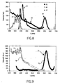
- the first series of measurements shown in Figures 8 and 9 illustrates the energy transfer between a transfer molecule and QDs using excitation spectra from two scenarios; 1) with the transfer molecule not being attached to the QD and 2) with the transfer molecule being attached to the QD.
- Spectrum 66 is an excitation spectrum corresponding to anthracene emission at 440nm.
- the emission at 440nm (coming from anthracene) is monitored while the excitation wavelength is scanned.
- the resulting spectrum shows the strength of the 440nm emission as a function of excitation wavelength, thereby indicating how much of the excitation at a given wavelength results in emission at 440nm.
- the excitation peaks 67 are the anthracene excitation spectrum.
- an excitation spectrum 68 corresponding to QD emission at 610nm. It can be seen that the 610nm emission mainly corresponds to QD absorption. The absence of the anthracene absorption peaks 67 in this spectrum indicates that there is almost no energy transfer from anthracene to QD.
- Figure 9 also shows an excitation spectrum 78 corresponding to QD emission at 610nm, similar to the excitation spectrum 68 of Figure 8 .
- Excitation spectrum 78 clearly shows anthracene absorption peaks 77 superimposed on the QD absorption. This proves that anthracene absorption contributes to the 610nm QD emission, and clearly indicates the presence of energy transfer from anthracene to QDs.
- Figures 8 and 9 illustrate the second step of the two step energy transfer, transfer of excitons from the transfer molecule to the QD.
- the behaviour observed for the dry film is totally different than the behaviour observed for the solution.
- excitons created in the transfer molecule are transferred to the QD at a rate which is larger than their decay rate in anthracene.
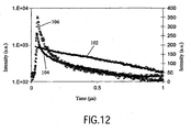
- triplet emitters which are known to have long decay times.
- an emission spectrum 82 of a layer containing 80% QDs and 20% triplet emitter is shown together with an emission spectrum 84 from the pure triplet emitter.
- curve 92 shows an excitation spectrum for the 620nm emission peak of Figure 10 , corresponding to the quantum dot emission, for a pure QD layer.
- Curve 94 also shows an excitation spectrum for the 620nm QD emission peak, but for the layer containing 80% QDs and 20% triplet emitter. It can be seen that there is a much larger contribution to the QD emission in the spectrum 94 for the layer containing 80% QDs and 20% triplet emitter, indicating that much of the 620nm emission originates in absorption in the triplet emitter.
- Figure 11 also shows curve 96 which is spectrum 94 corrected for the quantum dot absorption (spectrum 92) and for the triplet emitters contribution to the emission at 620nm (Spectrum 84 of Figure 10 shows that the triplet emitter also emits at 620nm, the monitored 620nm emission are corrected for this contribution). After these corrections, it can be seen that there is still a contribution by the triplet emitter to the QD emission.
Landscapes
- Engineering & Computer Science (AREA)
- Chemical & Material Sciences (AREA)
- Nanotechnology (AREA)
- Physics & Mathematics (AREA)
- Crystallography & Structural Chemistry (AREA)
- Optics & Photonics (AREA)
- Composite Materials (AREA)
- Biophysics (AREA)
- Life Sciences & Earth Sciences (AREA)
- Condensed Matter Physics & Semiconductors (AREA)
- General Physics & Mathematics (AREA)
- Materials Engineering (AREA)
- Mathematical Physics (AREA)
- Theoretical Computer Science (AREA)
- Inorganic Chemistry (AREA)
- Electroluminescent Light Sources (AREA)
- Luminescent Compositions (AREA)
Priority Applications (1)
| Application Number | Priority Date | Filing Date | Title |
|---|---|---|---|
| EP04799218A EP1692732B1 (en) | 2003-12-02 | 2004-11-23 | Electroluminescent device |
Applications Claiming Priority (3)
| Application Number | Priority Date | Filing Date | Title |
|---|---|---|---|
| EP03104494 | 2003-12-02 | ||
| PCT/IB2004/052519 WO2005055330A1 (en) | 2003-12-02 | 2004-11-23 | Electroluminescent device |
| EP04799218A EP1692732B1 (en) | 2003-12-02 | 2004-11-23 | Electroluminescent device |
Publications (2)
| Publication Number | Publication Date |
|---|---|
| EP1692732A1 EP1692732A1 (en) | 2006-08-23 |
| EP1692732B1 true EP1692732B1 (en) | 2008-10-08 |
Family
ID=34639313
Family Applications (1)
| Application Number | Title | Priority Date | Filing Date |
|---|---|---|---|
| EP04799218A Active EP1692732B1 (en) | 2003-12-02 | 2004-11-23 | Electroluminescent device |
Country Status (9)
| Country | Link |
|---|---|
| US (1) | US20070077594A1 (zh) |
| EP (1) | EP1692732B1 (zh) |
| JP (1) | JP5105878B2 (zh) |
| KR (1) | KR20060111545A (zh) |
| CN (1) | CN1886844B (zh) |
| AT (1) | ATE410792T1 (zh) |
| DE (1) | DE602004017049D1 (zh) |
| TW (1) | TW200524193A (zh) |
| WO (1) | WO2005055330A1 (zh) |
Cited By (1)
| Publication number | Priority date | Publication date | Assignee | Title |
|---|---|---|---|---|
| WO2011147522A1 (en) * | 2010-05-27 | 2011-12-01 | Merck Patent Gmbh | Compositions comprising quantum dots |
Families Citing this family (73)
| Publication number | Priority date | Publication date | Assignee | Title |
|---|---|---|---|---|
| JP2006083219A (ja) | 2004-09-14 | 2006-03-30 | Sharp Corp | 蛍光体およびこれを用いた発光装置 |
| US8101941B2 (en) * | 2005-09-26 | 2012-01-24 | Osram Opto Semiconductors Gmbh | Interface conditioning to improve efficiency and lifetime of organic electroluminescence devices |
| US9951438B2 (en) | 2006-03-07 | 2018-04-24 | Samsung Electronics Co., Ltd. | Compositions, optical component, system including an optical component, devices, and other products |
| KR100764847B1 (ko) | 2006-03-29 | 2007-10-09 | 한국화학연구원 | 저 homo 에너지 준위 유기반도체재료를 이용한 양자점발광소자 |
| WO2008111947A1 (en) | 2006-06-24 | 2008-09-18 | Qd Vision, Inc. | Methods and articles including nanomaterial |
| WO2008105792A2 (en) | 2006-06-24 | 2008-09-04 | Qd Vision, Inc. | Methods for depositing nanomaterial, methods for fabricating a device, methods for fabricating an array of devices and compositions |
| KR101282400B1 (ko) * | 2006-08-24 | 2013-07-04 | 한국과학기술원 | 유기 발광 표시 장치 |
| WO2008033388A2 (en) * | 2006-09-12 | 2008-03-20 | Qd Vision, Inc. | A composite including nanoparticles, methods, and products including a composite |
| DE102006061909A1 (de) * | 2006-12-21 | 2008-06-26 | Samsung SDI Co., Ltd., Suwon | Emitterschicht für eine organische Leuchtdiode |
| US7952105B2 (en) | 2007-01-29 | 2011-05-31 | Global Oled Technology, Llc. | Light-emitting display device having improved efficiency |
| US20080218068A1 (en) | 2007-03-05 | 2008-09-11 | Cok Ronald S | Patterned inorganic led device |
| US20100110728A1 (en) | 2007-03-19 | 2010-05-06 | Nanosys, Inc. | Light-emitting diode (led) devices comprising nanocrystals |
| KR101686669B1 (ko) * | 2007-03-19 | 2016-12-14 | 나노시스, 인크. | 나노크리스털을 캡슐화하는 방법 |
| TWI410162B (zh) * | 2007-06-07 | 2013-09-21 | Nat Univ Tsing Hua | 含奈米點之有機發光二極體裝置結構 |
| WO2009014590A2 (en) | 2007-06-25 | 2009-01-29 | Qd Vision, Inc. | Compositions and methods including depositing nanomaterial |
| WO2009014707A2 (en) | 2007-07-23 | 2009-01-29 | Qd Vision, Inc. | Quantum dot light enhancement substrate and lighting device including same |
| JP5407242B2 (ja) * | 2007-09-28 | 2014-02-05 | 大日本印刷株式会社 | エレクトロルミネッセンス素子 |
| JP5267009B2 (ja) | 2007-09-28 | 2013-08-21 | 大日本印刷株式会社 | 発光デバイス |
| JP5176459B2 (ja) * | 2007-09-28 | 2013-04-03 | 大日本印刷株式会社 | 白色発光素子 |
| WO2009041595A1 (ja) * | 2007-09-28 | 2009-04-02 | Dai Nippon Printing Co., Ltd. | エレクトロルミネッセンス素子 |
| WO2009041594A1 (ja) * | 2007-09-28 | 2009-04-02 | Dai Nippon Printing Co., Ltd. | エレクトロルミネッセンス素子 |
| JP2009087744A (ja) * | 2007-09-28 | 2009-04-23 | Dainippon Printing Co Ltd | 発光素子 |
| WO2009041689A1 (ja) * | 2007-09-28 | 2009-04-02 | Dai Nippon Printing Co., Ltd. | 発光デバイス |
| JP5407241B2 (ja) | 2007-09-28 | 2014-02-05 | 大日本印刷株式会社 | エレクトロルミネッセンス素子 |
| US20100224859A1 (en) * | 2007-10-16 | 2010-09-09 | Hcf Partners, Lp | Organic Light-Emitting Diodes with Electrophosphorescent-Coated Emissive Quantum Dots |
| WO2009081918A1 (ja) * | 2007-12-26 | 2009-07-02 | Idemitsu Kosan Co., Ltd. | 有機・無機ハイブリッド型電界発光素子 |
| DE102008006955B4 (de) * | 2008-01-31 | 2010-07-22 | Fraunhofer-Gesellschaft zur Förderung der angewandten Forschung e.V. | Herstellung und Applikationen multifunktionaler optischer Module zur photovoltaischen Stromerzeugung und für Beleuchtungszwecke |
| US8164083B2 (en) * | 2008-10-14 | 2012-04-24 | Brother International Corporation | Quantum dot optoelectronic devices with enhanced performance |
| EP2180030A3 (en) | 2008-10-23 | 2010-10-06 | National Tsing Hua University | Organic light emitting diode with nano-dots and fabrication method thereof |
| TWI422088B (zh) * | 2008-10-23 | 2014-01-01 | Nat Univ Tsing Hua | 具有奈米點之有機發光二極體及其製造方法 |
| US10214686B2 (en) | 2008-12-30 | 2019-02-26 | Nanosys, Inc. | Methods for encapsulating nanocrystals and resulting compositions |
| US11198270B2 (en) | 2008-12-30 | 2021-12-14 | Nanosys, Inc. | Quantum dot films, lighting devices, and lighting methods |
| US8343575B2 (en) | 2008-12-30 | 2013-01-01 | Nanosys, Inc. | Methods for encapsulating nanocrystals and resulting compositions |
| KR101097342B1 (ko) * | 2010-03-09 | 2011-12-23 | 삼성모바일디스플레이주식회사 | 양자점 유기 전계 발광 소자 및 그 형성방법 |
| KR101274068B1 (ko) * | 2010-05-25 | 2013-06-12 | 서울대학교산학협력단 | 양자점 발광 소자 및 이를 이용한 디스플레이 |
| CN106887522B (zh) * | 2010-07-26 | 2018-09-18 | 默克专利有限公司 | 包含纳米晶体的器件 |
| EP2599141B1 (en) * | 2010-07-26 | 2019-12-11 | Merck Patent GmbH | Quantum dots and hosts |
| EP2638321B1 (en) | 2010-11-10 | 2019-05-08 | Nanosys, Inc. | Quantum dot films, lighting devices, and lighting methods |
| WO2012108532A1 (ja) * | 2011-02-10 | 2012-08-16 | 株式会社ブリヂストン | 発光素子 |
| US8847198B2 (en) | 2011-05-26 | 2014-09-30 | Micron Technology, Inc. | Light emitting devices with built-in chromaticity conversion and methods of manufacturing |
| CN103999249B (zh) * | 2011-10-31 | 2017-08-11 | 南洋理工大学 | 发光装置 |
| US9929325B2 (en) | 2012-06-05 | 2018-03-27 | Samsung Electronics Co., Ltd. | Lighting device including quantum dots |
| WO2014057968A1 (ja) * | 2012-10-10 | 2014-04-17 | コニカミノルタ株式会社 | エレクトロルミネッセンス素子 |
| JP2014187283A (ja) * | 2013-03-25 | 2014-10-02 | Kaneka Corp | 有機el装置 |
| CN103427049B (zh) * | 2013-08-21 | 2014-12-03 | 京东方科技集团股份有限公司 | 量子点发光元件的制造方法及量子点显示设备 |
| KR102327025B1 (ko) * | 2013-08-26 | 2021-11-16 | 가부시키가이샤 한도오따이 에네루기 켄큐쇼 | 발광 소자, 발광 장치, 표시 장치, 조명 장치, 및 전자 기기 |
| CN103474451A (zh) * | 2013-09-12 | 2013-12-25 | 深圳市华星光电技术有限公司 | 彩色oled器件及其制作方法 |
| CN103956432A (zh) | 2014-04-14 | 2014-07-30 | 京东方科技集团股份有限公司 | 一种发光二极管及电子设备 |
| CN104021735B (zh) * | 2014-05-23 | 2016-08-17 | 京东方科技集团股份有限公司 | 一种量子点发光显示屏及其制备方法 |
| US10903440B2 (en) | 2015-02-24 | 2021-01-26 | Semiconductor Energy Laboratory Co., Ltd. | Light-emitting element, light-emitting device, electronic device, and lighting device |
| CN104795508B (zh) * | 2015-04-21 | 2017-03-15 | 苏州大学 | 一种柔性oled器件结构及其制备方法 |
| CN104868026B (zh) * | 2015-05-22 | 2019-02-22 | 深圳市华星光电技术有限公司 | 量子点发光元件 |
| CN104993069A (zh) * | 2015-06-09 | 2015-10-21 | 宁波工程学院 | 基于Cu掺杂多元量子点溶液加工发光二极管的构建方法 |
| CN105161579A (zh) * | 2015-08-17 | 2015-12-16 | 深圳市华星光电技术有限公司 | 掺杂金属的量子点及led器件和背光模组 |
| CN105449111B (zh) * | 2016-01-08 | 2018-03-20 | 京东方科技集团股份有限公司 | 具有结合层的量子点发光二极管基板及其制备方法 |
| CN105552245B (zh) * | 2016-02-18 | 2017-07-28 | 京东方科技集团股份有限公司 | 电致发光器件及其制作方法、显示装置 |
| CN105845837B (zh) * | 2016-04-07 | 2018-05-29 | 上海大学 | 倒置绿光量子点薄膜电致发光器件及其制备方法 |
| CN105826482B (zh) * | 2016-04-07 | 2017-12-22 | 上海大学 | 绿光量子点薄膜电致发光器件及其制备方法 |
| TWI599078B (zh) * | 2016-08-05 | 2017-09-11 | 行家光電股份有限公司 | 具濕氣阻隔結構之晶片級封裝發光裝置 |
| EP3279952A1 (en) | 2016-08-05 | 2018-02-07 | Maven Optronics Co., Ltd. | Moisture-resistant chip scale packaging light-emitting device |
| CN106356462A (zh) * | 2016-08-23 | 2017-01-25 | 苏州星烁纳米科技有限公司 | 包括量子点和能量转移分子的发光二极管装置及其制备方法、显示装置 |
| CN106549109A (zh) * | 2016-10-25 | 2017-03-29 | Tcl集团股份有限公司 | 一种基于p‑i‑n结构的QLED器件及其制备方法 |
| US20180175319A1 (en) | 2016-12-15 | 2018-06-21 | Universal Display Corporation | Spectral emission modification using localized surface plasmon of metallic nanoparticles |
| DE102017111425A1 (de) * | 2017-05-24 | 2018-11-29 | Osram Oled Gmbh | Organisches elektronisches Bauelement und Verfahren zur Herstellung eines organischen elektronischen Bauelements |
| JP7307046B2 (ja) * | 2018-02-15 | 2023-07-11 | 国立大学法人大阪大学 | コアシェル型半導体ナノ粒子、その製造方法および発光デバイス |
| JP7002367B2 (ja) * | 2018-03-07 | 2022-01-20 | 株式会社ジャパンディスプレイ | 表示装置 |
| US20210159438A1 (en) * | 2018-04-11 | 2021-05-27 | Nanoco Technologies Ltd. | Quantum dot architectures for fluorescence donor-assisted oled devices |
| CN109166977B (zh) * | 2018-08-29 | 2020-09-04 | 合肥工业大学 | 基于双侧氧化锌和p型有机主体的量子点电致发光器件 |
| CN113227316A (zh) | 2018-11-16 | 2021-08-06 | 九州有机光材股份有限公司 | 电致发光显示器件及其制造方法 |
| CN109801951B (zh) * | 2019-02-13 | 2022-07-12 | 京东方科技集团股份有限公司 | 阵列基板、电致发光显示面板及显示装置 |
| KR102200111B1 (ko) * | 2019-07-26 | 2021-01-08 | 한양대학교 산학협력단 | 양자점을 포함하는 유기 발광 표시 장치 |
| CN112331775B (zh) * | 2019-10-21 | 2023-04-07 | 广东聚华印刷显示技术有限公司 | 量子点发光器件及其制备方法、发光装置 |
| CN112331776B (zh) * | 2019-10-23 | 2023-07-25 | 广东聚华印刷显示技术有限公司 | 量子点发光器件及其制备方法、显示装置 |
Family Cites Families (13)
| Publication number | Priority date | Publication date | Assignee | Title |
|---|---|---|---|---|
| JPH0734396B2 (ja) * | 1989-11-21 | 1995-04-12 | ジェイ・イー・エル株式会社 | 厚膜印刷による薄形ディスプレイパネル及びその製造方法 |
| JPH0845669A (ja) * | 1994-07-28 | 1996-02-16 | Casio Comput Co Ltd | 平面型発光パネル |
| US6605904B2 (en) * | 2000-01-31 | 2003-08-12 | University Of Rochester | Tunable multicolor electroluminescent device |
| JP2001279240A (ja) * | 2000-03-29 | 2001-10-10 | Toshiba Corp | 発光体粒子及び発光デバイス |
| JP5062797B2 (ja) * | 2000-05-22 | 2012-10-31 | 昭和電工株式会社 | 有機エレクトロルミネッセンス素子および発光材料 |
| JP2002343570A (ja) * | 2001-05-15 | 2002-11-29 | Canon Inc | 導電性液晶素子及び有機エレクトロルミネッセンス素子 |
| JP4036018B2 (ja) * | 2001-06-20 | 2008-01-23 | 昭和電工株式会社 | 有機発光素子および発光材料 |
| WO2003021694A2 (en) * | 2001-09-04 | 2003-03-13 | Koninklijke Philips Electronics N.V. | Electroluminescent device comprising quantum dots |
| TW519852B (en) * | 2001-10-18 | 2003-02-01 | Opto Tech Corp | Organic light emitting device capable of projecting white light source and its manufacturing method |
| US6984460B2 (en) * | 2002-03-26 | 2006-01-10 | Tdk Corporation | Phosphor thin film, manufacturing method of the same, and electroluminescence panel |
| EP2557139B1 (en) * | 2002-03-29 | 2021-05-05 | Massachusetts Institute Of Technology | Light emitting device including semiconductor nanocrystals |
| WO2004023527A2 (en) * | 2002-09-05 | 2004-03-18 | Nanosys, Inc. | Nanostructure and nanocomposite based compositions and photovoltaic devices |
| US7065285B2 (en) * | 2003-12-01 | 2006-06-20 | Lucent Technologies Inc. | Polymeric compositions comprising quantum dots, optical devices comprising these compositions and methods for preparing same |
-
2004
- 2004-11-23 EP EP04799218A patent/EP1692732B1/en active Active
- 2004-11-23 JP JP2006542074A patent/JP5105878B2/ja active Active
- 2004-11-23 KR KR1020067010724A patent/KR20060111545A/ko not_active Application Discontinuation
- 2004-11-23 WO PCT/IB2004/052519 patent/WO2005055330A1/en not_active Application Discontinuation
- 2004-11-23 CN CN2004800355889A patent/CN1886844B/zh active Active
- 2004-11-23 DE DE602004017049T patent/DE602004017049D1/de active Active
- 2004-11-23 AT AT04799218T patent/ATE410792T1/de not_active IP Right Cessation
- 2004-11-23 US US10/581,133 patent/US20070077594A1/en not_active Abandoned
- 2004-11-29 TW TW093136762A patent/TW200524193A/zh unknown
Cited By (1)
| Publication number | Priority date | Publication date | Assignee | Title |
|---|---|---|---|---|
| WO2011147522A1 (en) * | 2010-05-27 | 2011-12-01 | Merck Patent Gmbh | Compositions comprising quantum dots |
Also Published As
| Publication number | Publication date |
|---|---|
| CN1886844A (zh) | 2006-12-27 |
| WO2005055330A1 (en) | 2005-06-16 |
| CN1886844B (zh) | 2010-06-09 |
| KR20060111545A (ko) | 2006-10-27 |
| JP2007513478A (ja) | 2007-05-24 |
| EP1692732A1 (en) | 2006-08-23 |
| ATE410792T1 (de) | 2008-10-15 |
| JP5105878B2 (ja) | 2012-12-26 |
| DE602004017049D1 (de) | 2008-11-20 |
| US20070077594A1 (en) | 2007-04-05 |
| TW200524193A (en) | 2005-07-16 |
Similar Documents
| Publication | Publication Date | Title |
|---|---|---|
| EP1692732B1 (en) | Electroluminescent device | |
| US11005058B2 (en) | Light-emitting device including quantum dots | |
| US10403690B2 (en) | Light emitting device including tandem structure with quantum dots and nanoparticles | |
| JP6685362B2 (ja) | 発光ダイオードおよびこれを備える発光装置 | |
| JP4153694B2 (ja) | 有機el素子および表示装置 | |
| JP2005502176A (ja) | 量子ドットを有するエレクトロルミネセント装置 | |
| Li et al. | Bright white‐light‐emitting device from ternary nanocrystal composites | |
| Forrest | Active optoelectronics using thin-film organic semiconductors | |
| Holder et al. | Hybrid nanocomposite materials with organic and inorganic components for opto-electronic devices | |
| CN109713098A (zh) | 发光二极管以及包括该发光二极管的发光设备 | |
| US20100244062A1 (en) | White light emitting element | |
| CN109585623A (zh) | 发光二极管以及包括其的发光装置 | |
| KR20100089818A (ko) | 발광소자 | |
| KR20060018583A (ko) | 반도체 나노결정을 함유하는 백색 발광 유·무기하이브리드 전기 발광 소자 | |
| KR100426919B1 (ko) | 유기 전계 발광 소자 및 표시 장치 | |
| JP2013518373A (ja) | 色変換のための集積層を有する有機エレクトロルミネッセンスデバイス | |
| WO2011044391A1 (en) | Device including quantum dots | |
| US11398580B2 (en) | Light emitting diode and light emitting device including the same | |
| CN109698259A (zh) | 应用各向异性纳米棒的发光二极管及包括其的发光装置 | |
| JP2009087754A (ja) | 発光素子 | |
| GB2516929A (en) | Light Emitting Device | |
| Chou et al. | Hybrid white-light emitting-LED based on luminescent polyfluorene polymer and quantum dots | |
| US11502267B2 (en) | Inorganic light emitting diode and inorganic light emitting device including the same | |
| Kwon et al. | Hybrid two-color pink emission device of perovskite red quantum dot materials using organic blue emitter | |
| Srivastava et al. | Organic light emitting diodes for white light emission |
Legal Events
| Date | Code | Title | Description |
|---|---|---|---|
| PUAI | Public reference made under article 153(3) epc to a published international application that has entered the european phase |
Free format text: ORIGINAL CODE: 0009012 |
|
| 17P | Request for examination filed |
Effective date: 20060703 |
|
| AK | Designated contracting states |
Kind code of ref document: A1 Designated state(s): AT BE BG CH CY CZ DE DK EE ES FI FR GB GR HU IE IS IT LI LU MC NL PL PT RO SE SI SK TR |
|
| 17Q | First examination report despatched |
Effective date: 20061214 |
|
| DAX | Request for extension of the european patent (deleted) | ||
| GRAP | Despatch of communication of intention to grant a patent |
Free format text: ORIGINAL CODE: EPIDOSNIGR1 |
|
| RIC1 | Information provided on ipc code assigned before grant |
Ipc: H01L 51/50 20060101AFI20080317BHEP |
|
| GRAS | Grant fee paid |
Free format text: ORIGINAL CODE: EPIDOSNIGR3 |
|
| GRAA | (expected) grant |
Free format text: ORIGINAL CODE: 0009210 |
|
| AK | Designated contracting states |
Kind code of ref document: B1 Designated state(s): AT BE BG CH CY CZ DE DK EE ES FI FR GB GR HU IE IS IT LI LU MC NL PL PT RO SE SI SK TR |
|
| REG | Reference to a national code |
Ref country code: GB Ref legal event code: FG4D |
|
| REG | Reference to a national code |
Ref country code: CH Ref legal event code: EP |
|
| REG | Reference to a national code |
Ref country code: IE Ref legal event code: FG4D |
|
| REF | Corresponds to: |
Ref document number: 602004017049 Country of ref document: DE Date of ref document: 20081120 Kind code of ref document: P |
|
| PG25 | Lapsed in a contracting state [announced via postgrant information from national office to epo] |
Ref country code: SI Free format text: LAPSE BECAUSE OF FAILURE TO SUBMIT A TRANSLATION OF THE DESCRIPTION OR TO PAY THE FEE WITHIN THE PRESCRIBED TIME-LIMIT Effective date: 20081008 |
|
| NLV1 | Nl: lapsed or annulled due to failure to fulfill the requirements of art. 29p and 29m of the patents act | ||
| PG25 | Lapsed in a contracting state [announced via postgrant information from national office to epo] |
Ref country code: ES Free format text: LAPSE BECAUSE OF FAILURE TO SUBMIT A TRANSLATION OF THE DESCRIPTION OR TO PAY THE FEE WITHIN THE PRESCRIBED TIME-LIMIT Effective date: 20090119 Ref country code: AT Free format text: LAPSE BECAUSE OF FAILURE TO SUBMIT A TRANSLATION OF THE DESCRIPTION OR TO PAY THE FEE WITHIN THE PRESCRIBED TIME-LIMIT Effective date: 20081008 Ref country code: BG Free format text: LAPSE BECAUSE OF FAILURE TO SUBMIT A TRANSLATION OF THE DESCRIPTION OR TO PAY THE FEE WITHIN THE PRESCRIBED TIME-LIMIT Effective date: 20090108 |
|
| PG25 | Lapsed in a contracting state [announced via postgrant information from national office to epo] |
Ref country code: PL Free format text: LAPSE BECAUSE OF FAILURE TO SUBMIT A TRANSLATION OF THE DESCRIPTION OR TO PAY THE FEE WITHIN THE PRESCRIBED TIME-LIMIT Effective date: 20081008 Ref country code: FI Free format text: LAPSE BECAUSE OF FAILURE TO SUBMIT A TRANSLATION OF THE DESCRIPTION OR TO PAY THE FEE WITHIN THE PRESCRIBED TIME-LIMIT Effective date: 20081008 Ref country code: PT Free format text: LAPSE BECAUSE OF FAILURE TO SUBMIT A TRANSLATION OF THE DESCRIPTION OR TO PAY THE FEE WITHIN THE PRESCRIBED TIME-LIMIT Effective date: 20090218 Ref country code: NL Free format text: LAPSE BECAUSE OF FAILURE TO SUBMIT A TRANSLATION OF THE DESCRIPTION OR TO PAY THE FEE WITHIN THE PRESCRIBED TIME-LIMIT Effective date: 20081008 Ref country code: IS Free format text: LAPSE BECAUSE OF FAILURE TO SUBMIT A TRANSLATION OF THE DESCRIPTION OR TO PAY THE FEE WITHIN THE PRESCRIBED TIME-LIMIT Effective date: 20090208 |
|
| PG25 | Lapsed in a contracting state [announced via postgrant information from national office to epo] |
Ref country code: MC Free format text: LAPSE BECAUSE OF NON-PAYMENT OF DUE FEES Effective date: 20081130 |
|
| REG | Reference to a national code |
Ref country code: CH Ref legal event code: PL |
|
| PG25 | Lapsed in a contracting state [announced via postgrant information from national office to epo] |
Ref country code: DK Free format text: LAPSE BECAUSE OF FAILURE TO SUBMIT A TRANSLATION OF THE DESCRIPTION OR TO PAY THE FEE WITHIN THE PRESCRIBED TIME-LIMIT Effective date: 20081008 Ref country code: RO Free format text: LAPSE BECAUSE OF FAILURE TO SUBMIT A TRANSLATION OF THE DESCRIPTION OR TO PAY THE FEE WITHIN THE PRESCRIBED TIME-LIMIT Effective date: 20081008 Ref country code: BE Free format text: LAPSE BECAUSE OF FAILURE TO SUBMIT A TRANSLATION OF THE DESCRIPTION OR TO PAY THE FEE WITHIN THE PRESCRIBED TIME-LIMIT Effective date: 20081008 Ref country code: EE Free format text: LAPSE BECAUSE OF FAILURE TO SUBMIT A TRANSLATION OF THE DESCRIPTION OR TO PAY THE FEE WITHIN THE PRESCRIBED TIME-LIMIT Effective date: 20081008 |
|
| PLBE | No opposition filed within time limit |
Free format text: ORIGINAL CODE: 0009261 |
|
| STAA | Information on the status of an ep patent application or granted ep patent |
Free format text: STATUS: NO OPPOSITION FILED WITHIN TIME LIMIT |
|
| REG | Reference to a national code |
Ref country code: IE Ref legal event code: MM4A |
|
| PG25 | Lapsed in a contracting state [announced via postgrant information from national office to epo] |
Ref country code: SE Free format text: LAPSE BECAUSE OF FAILURE TO SUBMIT A TRANSLATION OF THE DESCRIPTION OR TO PAY THE FEE WITHIN THE PRESCRIBED TIME-LIMIT Effective date: 20090108 Ref country code: CZ Free format text: LAPSE BECAUSE OF FAILURE TO SUBMIT A TRANSLATION OF THE DESCRIPTION OR TO PAY THE FEE WITHIN THE PRESCRIBED TIME-LIMIT Effective date: 20081008 Ref country code: IT Free format text: LAPSE BECAUSE OF FAILURE TO SUBMIT A TRANSLATION OF THE DESCRIPTION OR TO PAY THE FEE WITHIN THE PRESCRIBED TIME-LIMIT Effective date: 20081008 |
|
| 26N | No opposition filed |
Effective date: 20090709 |
|
| PG25 | Lapsed in a contracting state [announced via postgrant information from national office to epo] |
Ref country code: SK Free format text: LAPSE BECAUSE OF FAILURE TO SUBMIT A TRANSLATION OF THE DESCRIPTION OR TO PAY THE FEE WITHIN THE PRESCRIBED TIME-LIMIT Effective date: 20081008 |
|
| PG25 | Lapsed in a contracting state [announced via postgrant information from national office to epo] |
Ref country code: IE Free format text: LAPSE BECAUSE OF NON-PAYMENT OF DUE FEES Effective date: 20081123 Ref country code: CH Free format text: LAPSE BECAUSE OF NON-PAYMENT OF DUE FEES Effective date: 20081130 Ref country code: LI Free format text: LAPSE BECAUSE OF NON-PAYMENT OF DUE FEES Effective date: 20081130 |
|
| PG25 | Lapsed in a contracting state [announced via postgrant information from national office to epo] |
Ref country code: HU Free format text: LAPSE BECAUSE OF FAILURE TO SUBMIT A TRANSLATION OF THE DESCRIPTION OR TO PAY THE FEE WITHIN THE PRESCRIBED TIME-LIMIT Effective date: 20090409 Ref country code: CY Free format text: LAPSE BECAUSE OF FAILURE TO SUBMIT A TRANSLATION OF THE DESCRIPTION OR TO PAY THE FEE WITHIN THE PRESCRIBED TIME-LIMIT Effective date: 20081008 Ref country code: LU Free format text: LAPSE BECAUSE OF NON-PAYMENT OF DUE FEES Effective date: 20081123 |
|
| PG25 | Lapsed in a contracting state [announced via postgrant information from national office to epo] |
Ref country code: TR Free format text: LAPSE BECAUSE OF FAILURE TO SUBMIT A TRANSLATION OF THE DESCRIPTION OR TO PAY THE FEE WITHIN THE PRESCRIBED TIME-LIMIT Effective date: 20081008 |
|
| PG25 | Lapsed in a contracting state [announced via postgrant information from national office to epo] |
Ref country code: GR Free format text: LAPSE BECAUSE OF FAILURE TO SUBMIT A TRANSLATION OF THE DESCRIPTION OR TO PAY THE FEE WITHIN THE PRESCRIBED TIME-LIMIT Effective date: 20090109 |
|
| REG | Reference to a national code |
Ref country code: DE Ref legal event code: R082 Ref document number: 602004017049 Country of ref document: DE Representative=s name: MEISSNER, BOLTE & PARTNER GBR, DE |
|
| REG | Reference to a national code |
Ref country code: DE Ref legal event code: R081 Ref document number: 602004017049 Country of ref document: DE Owner name: KONINKLIJKE PHILIPS N.V., NL Free format text: FORMER OWNER: KONINKLIJKE PHILIPS ELECTRONICS N.V., EINDHOVEN, NL Effective date: 20140328 Ref country code: DE Ref legal event code: R082 Ref document number: 602004017049 Country of ref document: DE Representative=s name: MEISSNER, BOLTE & PARTNER GBR, DE Effective date: 20140328 Ref country code: DE Ref legal event code: R082 Ref document number: 602004017049 Country of ref document: DE Representative=s name: MEISSNER BOLTE PATENTANWAELTE RECHTSANWAELTE P, DE Effective date: 20140328 Ref country code: DE Ref legal event code: R082 Ref document number: 602004017049 Country of ref document: DE Representative=s name: DOMPATENT VON KREISLER SELTING WERNER - PARTNE, DE Effective date: 20140328 |
|
| REG | Reference to a national code |
Ref country code: FR Ref legal event code: CA Effective date: 20141126 Ref country code: FR Ref legal event code: CD Owner name: KONINKLIJKE PHILIPS N.V., NL Effective date: 20141126 |
|
| REG | Reference to a national code |
Ref country code: FR Ref legal event code: PLFP Year of fee payment: 12 |
|
| REG | Reference to a national code |
Ref country code: FR Ref legal event code: PLFP Year of fee payment: 13 |
|
| REG | Reference to a national code |
Ref country code: FR Ref legal event code: PLFP Year of fee payment: 14 |
|
| REG | Reference to a national code |
Ref country code: DE Ref legal event code: R082 Ref document number: 602004017049 Country of ref document: DE Representative=s name: DOMPATENT VON KREISLER SELTING WERNER - PARTNE, DE |
|
| REG | Reference to a national code |
Ref country code: GB Ref legal event code: 732E Free format text: REGISTERED BETWEEN 20180809 AND 20180815 |
|
| REG | Reference to a national code |
Ref country code: DE Ref legal event code: R082 Ref document number: 602004017049 Country of ref document: DE Representative=s name: DOMPATENT VON KREISLER SELTING WERNER - PARTNE, DE Ref country code: DE Ref legal event code: R081 Ref document number: 602004017049 Country of ref document: DE Owner name: BEIJING XIAOMI MOBILE SOFTWARE CO., LTD., CN Free format text: FORMER OWNER: KONINKLIJKE PHILIPS N.V., EINDHOVEN, NL |
|
| REG | Reference to a national code |
Ref country code: DE Ref legal event code: R079 Ref document number: 602004017049 Country of ref document: DE Free format text: PREVIOUS MAIN CLASS: H01L0051000000 Ipc: H10K0099000000 |
|
| P01 | Opt-out of the competence of the unified patent court (upc) registered |
Effective date: 20230531 |
|
| PGFP | Annual fee paid to national office [announced via postgrant information from national office to epo] |
Ref country code: GB Payment date: 20231123 Year of fee payment: 20 |
|
| PGFP | Annual fee paid to national office [announced via postgrant information from national office to epo] |
Ref country code: FR Payment date: 20231120 Year of fee payment: 20 Ref country code: DE Payment date: 20231121 Year of fee payment: 20 |