EP1687970B1 - Pixel signal binning and interpolation in column circuits of a sensor circuit - Google Patents
Pixel signal binning and interpolation in column circuits of a sensor circuit Download PDFInfo
- Publication number
- EP1687970B1 EP1687970B1 EP04810790.8A EP04810790A EP1687970B1 EP 1687970 B1 EP1687970 B1 EP 1687970B1 EP 04810790 A EP04810790 A EP 04810790A EP 1687970 B1 EP1687970 B1 EP 1687970B1
- Authority
- EP
- European Patent Office
- Prior art keywords
- column
- signal values
- circuit
- sample
- switches
- Prior art date
- Legal status (The legal status is an assumption and is not a legal conclusion. Google has not performed a legal analysis and makes no representation as to the accuracy of the status listed.)
- Not-in-force
Links
Images


Classifications
-
- H—ELECTRICITY
- H04—ELECTRIC COMMUNICATION TECHNIQUE
- H04N—PICTORIAL COMMUNICATION, e.g. TELEVISION
- H04N25/00—Circuitry of solid-state image sensors [SSIS]; Control thereof
- H04N25/40—Extracting pixel data from image sensors by controlling scanning circuits, e.g. by modifying the number of pixels sampled or to be sampled
- H04N25/46—Extracting pixel data from image sensors by controlling scanning circuits, e.g. by modifying the number of pixels sampled or to be sampled by combining or binning pixels
-
- H—ELECTRICITY
- H04—ELECTRIC COMMUNICATION TECHNIQUE
- H04N—PICTORIAL COMMUNICATION, e.g. TELEVISION
- H04N3/00—Scanning details of television systems; Combination thereof with generation of supply voltages
- H04N3/10—Scanning details of television systems; Combination thereof with generation of supply voltages by means not exclusively optical-mechanical
- H04N3/14—Scanning details of television systems; Combination thereof with generation of supply voltages by means not exclusively optical-mechanical by means of electrically scanned solid-state devices
- H04N3/15—Scanning details of television systems; Combination thereof with generation of supply voltages by means not exclusively optical-mechanical by means of electrically scanned solid-state devices for picture signal generation
- H04N3/155—Control of the image-sensor operation, e.g. image processing within the image-sensor
- H04N3/1562—Control of the image-sensor operation, e.g. image processing within the image-sensor for selective scanning, e.g. windowing, zooming
Definitions
- the present invention relates generally to image sensors, and, in particular, to charge-domain analog readout circuits for such sensors.
- Image sensors find applications in a wide variety of fields, including machine vision, robotics, guidance and navigation, automotive applications, and consumer products.
- CCD charge-coupled devices
- CMOS complementary metal-oxide-semiconductor
- a CCD is read out by sequentially transferring the signal charge through the semiconductor, and the readout rate is limited by the need for nearly perfect charge transfer.
- Active pixel sensors which have one or more active transistors within the pixel unit cell, can be made compatible with CMOS technologies and promise higher readout rates compared to passive pixel sensors.
- Active pixel sensors are often arranged as arrays of elements, which can be read out, for example, a column at a time. Each column can be read out at one time, driven and buffered for sensing by a readout circuit.
- FIG. 1 shows an exemplary CMOS active pixel sensor integrated circuit chip that includes an array of active pixel sensors 30 and a controller 32 that provides timing and control signals to enable the reading out of signals stored in the pixels.
- Exemplary arrays have dimensions of N by M pixels and, in general, the size of the array 30 will depend on the particular implementation.
- the imager is read out a row at a time using a column parallel readout architecture.
- the controller 32 selects a particular row of pixels in the array 30 by controlling the operation of vertical addressing circuit 34 and row drivers 40. Charge signals stored in the selected row of pixels are provided to a readout circuit 42.
- the pixels of the columns can be read out sequentially using a horizontal addressing circuit 44.
- each pixel provides a reset output signal V out1 and a signal representing accumulated charge during an integration period V out2 which are provided at the output of the readout circuit 42.
- the array 30 includes multiple columns 49 of CMOS active pixel sensors 50.
- Each column 49 includes multiple rows of sensors 50.
- Signals from the active pixel sensors 50 in a particular column can be read out to a readout circuit 52 associated with that column.
- Signals stored in the readout circuits 52 can be sent to an output stage 54, which is common to the entire array of pixels 30.
- the analog output signals can then be sent, for example, to a differential analog-to-digital converter (ADC).
- ADC differential analog-to-digital converter
- pixels are read out sequentially, but not contiguously. In other words, some pixels are skipped to obtain a lower resolution in exchange for a potentially higher frame rate. What is needed is an image sensor where the readout circuitry has improved sub-resolution characteristics with reduced aliasing.
- US Patent no. 6377304 describes Solid state image-pickup devices and associated circuit driving methods that provide a video signal with enhanced video frame refresh rates.
- Multiple pixels are arranged in a planar array of columns and rows. Each column has a separate vertical read-out line. The pixel outputs in each column are connected to a respective vertical read-out line.
- a vertical scanning circuit controllably switches the outputs of the pixels in each column to respective vertical read-out lines according to a predetermined horizontal-line read-out sequence.
- a multiplexer distributes the pixel output signals carried by the vertical read-out lines to multiple multiplexer outputs.
- a horizontal accumulator temporarily accumulates the pixel output signals for delivery to horizontal-accumulator outputs.
- Horizontal scanning means controllably trigger pixel output signals temporarily accumulated in the horizontal accumulator for sequential read-out onto horizontal read-out lines to form a video signal. The output signals from multiple adjacent pixels are simultaneously combined.
- the imager may be configured to provide an imager having multiresolution capability where SNR can be adjusted for optimum low-level detectibility.
- Multiresolution signal processing functionality is provided on-chip to achieve high speed imaging, employs an improved pixel binning approach with fully differential circuits situated so that extraneous and pick-up noise is eliminated.
- the implementation requires no frame transfer memory, thereby reducing chip size. The reduction in area enables larger area format light adaptive imager implementations.
- US Patent no. 5949483 describes an imaging device formed as a monolithic complementary metal oxide semiconductor integrated circuit in an industry standard complementary metal oxide semiconductor process, the integrated circuit including a focal plane array of pixel cells, each one of the cells including a photogate overlying the substrate for accumulating photogenerated charge in an underlying portion of the substrate and a charge coupled device section formed on the substrate adjacent the photogate having a sensing node and at least one charge coupled device stage for transferring charge from the underlying portion of the substrate to the sensing node.
- the imaging device can also include an electronic shutter formed on the substrate adjacent the photogate, and/or a storage section to allow for simultaneous integration.
- the imaging device can include a multiresolution imaging circuit to provide images of varying resolution.
- the multiresolution circuit could also be employed in an array where the photosensitive portion of each pixel cell is a photodiode. This latter embodiment could further be modified to facilitate low light imaging.
- embodiments of the invention provide an imaging circuit, system, and related methods for incorporating signal binning into the-readout circuitry.
- Binning is defined as accumulating or interpolating the charge of multiple pixels and reading them out in a single operation.
- various sub-resolution processes can be implemented to minimize aliasing effects.
- signal bandwidth may be reduced. This in turn reduces the overall power requirements of the sensor.
- An additional benefit to using analog binning is that the signal-to-noise ratio (SNR) advantages achieved from binning are more pronounced in the analog domain than they are in the digital domain.
- SNR signal-to-noise ratio
- FIG. 1 is a block diagram of an exemplary prior art CMOS active pixel sensor chip
- FIG. 2 is a block diagram of a conventional array of active pixel sensors and a readout circuit
- FIG. 3 is an exemplary charge mode readout circuit
- FIG. 4 shows vertical binning by implementing a split-capacitor configuration in accordance with an exemplary embodiment of the invention
- FIG. 5 illustrates a horizontal averaging scheme among column lines in accordance with another exemplary embodiment of the invention
- FIG. 6 illustrates a 1 ⁇ 2 capacitance line averaging circuit according to another exemplary embodiment of the invention
- FIG. 7 shows an exemplary color averaging operation for the circuit of FIG. 6 ;
- FIG. 8 illustrates an exemplary color averaging process for a first square of a pixel matrix in accordance with an exemplary embodiment of the invention
- FIG. 9 illustrates an exemplary color averaging process for a second square of a pixel matrix in accordance with an exemplary embodiment of the invention
- FIG. 10 illustrates an exemplary color averaging process for third and fourth squares of a pixel matrix in accordance with an exemplary embodiment of the invention
- FIG. 11 shows a binned pixel matrix after the averaging process of FIGs. 8-10 ;
- FIG. 12 is an exemplary configuration according to the invention that realizes a VGA Bayer pattern, where pixels are averaged from three rows and three columns;
- FIG. 13 illustrates a 2/3 resolution binning scheme according to the present invention, where two rows from three columns of a pixel matrix are averaged;
- FIG.14 illustrates a binning scheme according to the present invention, where every third column is skipped in order to average out two columns and two rows;
- FIG.15A illustrates an exemplary horizontal binning scheme that realizes a 1024x768 RGB resolution in accordance with another embodiment of the invention
- FIG. 15B illustrates an exemplary horizontal binning scheme that realizes a 1280x1024 RGB resolution in accordance with yet another embodiment of the invention
- FIG. 15C illustrates an exemplary horizontal binning scheme that realizes a "1/3 skip" VGA Bayer resolution in accordance with yet another embodiment of the invention
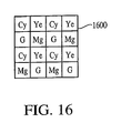
- FIG. 16 illustrates a Mg-Cy-Ye-G filter array from which color separation values are calculated in accordance with yet another embodiment of the invention
- FIG. 17 illustrates a block diagram of an imaging apparatus in accordance with yet another embodiment of the invention.
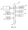
- FIG.18 illustrates a processing system that uses a binning circuit constructed in accordance with any of the embodiments of the invention.
- FIG 3 illustrates a differential charge-domain readout circuit 150 for an image sensor, wherein a column readout circuit 100 receives a signal from a pixel along a column line 101. Examples of such circuitry may be found in commonly-assigned U.S. patent no. 6,222,175 , .
- the readout circuit 100 includes a load transistor 102 that receives a signal (VLN) at its gate. As is known in the art, the VLN signal activates the load transistor 102 such that it provides a load on the column line 101.
- VLN signal
- the column line 101 is further coupled to two sample-and-hold circuits for storing a pixel signal level when a first sample-and-hold signal (SHS) is applied and a reset lever when a second sample-and-hold signal (SHR) is applied to the readout circuit 150.
- SHS sample-and-hold signal
- SHR second sample-and-hold signal
- CDS correlated double sampling
- the first sample-and-hold circuit includes a switch 103, which may be implemented as a transistor and a capacitor 106.
- the first sample-and-hold signal SHS is applied to the switch 103 to control whether the switch 103 is in a conductive or non-conductive state.
- the second sample-and-hold circuit also includes a switch 104, which also may be implemented as a transistor, and a capacitor 107.
- the second sample-and-hold signal SHR is applied to the switch 104 to control the state of the switch 104.
- Capacitors 106, 107 can be hold at a reference voltage (VCL) by closing switches 109, and 108, respectively.
- VCL reference voltage
- the column readout circuit 100 includes a crowbar switch 105, which also may be implemented as a transistor.
- the state of the crowbar transistor 105 is controlled by an external crowbar control signal (CB).
- CB external crowbar control signal
- Use of the crowbar switch 105 can help reduce fixed pattern noise (FPN) caused by column-to-column variations due to the column parallel readout structure (described above).
- Signals stored by the capacitors 106, 107 can be transmitted to the output stage 120 through respective column select switches 110, 111, which may be implemented as transistors.
- the column selection signal (ColSel) applied to the, switches 110, 111 controls whether those switches 110, 111 are conductive or non-conductive.
- the column selection switch 110 or 111
- the sampling capacitor 106 or 107
- both switches 110, 111 may be closed at the same time if desired. It should also be understood that any other suitable storage device may be substituted for the capacitors 106, 107.
- the output stage 120 of the charge-domain readout circuit 150 is common to the entire array 30 of pixels. Thus, although only a single circuit 150 is illustrated in FIG. 3 , multiple column readout circuits are coupled to the output stage 120.
- the output stage 120 includes a switched integrator, which further includes a differential operational amplifier 112, two feedback capacitors 113,114, respectively coupled between the output V out1 , V out2 and the negative and positive terminals of the operational amplifier 112. Reset switches 115,116 are respectively coupled between the output V out1 , V out2 and the negative and positive terminals of the operational amplifier 112.
- Each integrator output stage 120 can be selectively reset by turning on the associated reset switch 115,116 using a signal Rst_amp.
- the operational amplifier 112 provides two output signals V out1 , V out2 that are then transmitted to the analog-to-digital converter (not shown in FIG. 3 ).
- FIG. 4 illustrates an embodiment of the invention, wherein vertical binning is implemented in the readout circuit 100 of FIG. 3 .
- the capacitors 106, 107 of FIG. 3 are "split out" in the illustrated exemplary embodiment of FIG. 4 .
- the capacitive value of capacitors 106, 107 are replaced by multiple smaller capacitive elements 209-216, which each make up a fraction (e.g., 1 ⁇ 4) of the original capacitance.
- Each capacitor 209-216 is coupled to a respective switch 201-208, where each switch 201-208 is controllable to obtain different resolutions for an array 30 ( FIG. 2 ) under a predetermined sampling sequence.
- the capacitors 209-216 would essentially behave as one capacitor (i.e., full resolution), and the effective capacitance would be the same as that shown in FIG. 3 .
- FIG. 4 shows a four-capacitor configuration (i.e., each capacitor being split into 4 capacitive elements), any number of capacitor splits (2, 3, 4, 6, etc.) may be used.
- the readout circuit would be in a 1/2 resolution condition.
- the embodiment of FIG. 4 may be used with monochrome sensor schemes where the sensor may be configured to support full resolution, 1 ⁇ 2 resolution and 1 ⁇ 4 resolution in the vertical direction.
- the horizontal resolution is defined outside the chip.
- the signal received from a first row of the array is sampled and stored on two of the capacitors (e.g., capacitors 209-210 and 213-214) by enabling the respective switches (e.g., switches 201-202 and 205-206) associated with those capacitors.
- Signals received from a second row are sampled and stored on the two other capacitors (e.g., capacitors 211-212 and 215-216) by enabling their respective switches (e.g., switches 203-204 and 207-208).
- switches e.g., switches 203-204 and 207-208.
- the left plates of the capacitors 209-216 are shorted, wherein an averaged signal of the first and second rows is outputted. It should be noted that the gain of the circuit of FIG. 4 remains stable during this operation, which adds flexibility in using the circuit.
- signals received from the first four rows of a column are separately sampled to a respective capacitor 209-212, 213-216. After the four rows are stored, the left plates of the capacitors 209-216 are shorted to output an averaged signal among the four rows for the particular column.
- Bayer patterns are typically used to acquire color images when color sensing is used.
- Bayer color filter arrays are known in the art and are used to digitally acquire color images.
- the Bayer pattern of color filters are such that half the total number of pixels are green, while a quarter of the remaining pixels are red, and a quarter of the remaining pixels are blue.
- a color signal from a first row is read out and sampled on the first two capacitors 209-210, 213-214 of each sample line (i.e., pixel signals on capacitors 209-210, reset signals on capacitors 213-214).
- the signal on the third row is sampled to the other two capacitors 211-212, 215-216 of the sample lines.
- the four capacitors 209-212, 213-216 from each sample line are then shorted together; the averaged sum for rows 1 and 3 are read out (via switches 110,111). The same process is repeated with rows 2 and 4, where the row signals are averaged and read out as described above.
- the 1 ⁇ 4 resolution readout process for color signals is similar to the 1 ⁇ 2 resolution described above, where rows 1, 3, 5, and 7 are first stored on a respective capacitor 209-212, 213-216, averaged and read out; subsequently, rows 2, 4, 6, and 8 are stored on a respective capacitor 209-212, 213-216, averaged and read out.
- each binning circuit 500 has a sample and hold pixel signal and sample and hold reset signal node coupled to a neighboring circuit 501 via respective switches 502, 503.
- Binning circuit 501 also connects to a neighboring binning circuit (not shown) through switches 504, 505. Additional binning circuits can be added as required, and the outputs (BIN1 and BIN2) carry a "horizontally" averaged signal (i.e., average signal between the column circuits).
- FIG. 6 illustrates another embodiment of the invention, wherein the readout circuit 650 is similar to that discussed in FIG. 4 , except that each capacitor 604-605, 606-607 of a sample line makes up one-half (C/2) of each sample line capacitance (as opposed to the one-quarter shown in FIG. 4 ). Each capacitor 604-607 is coupled to a respective switch 600-603. Each of the switches 600-603 are controllable to obtain different (i.e., less-than-full and full) resolutions for the circuit 650 when opened and closed.
- the readout circuit 650 of FIG. 6 may be operated to sum together charges of the same pixel color in each column.
- the result from this kind of operation emulates that of a high resolution "skip mode" used in CCD devices, such as that used in the Sony ICX252AQ 3 Megapixel CCD.
- An exemplary operation of the FIG. 6 circuit 650 is shown in FIG. 7 , where the row selection algorithm in the readout circuit is configured to read out red colors (R) from rows 1 and 3 (700) and store them on capacitors 604-605.
- the reset signals from rows 1 and 3 are also read out (not shown) and stored on capacitors 606, 607.
- the left plates of the capacitors 604-607 are then shorted to output an averaged signal of the red colors of first and the third row.
- FIG. 7 continues with the green color (Gr) of rows 1 and 3, where the green colors (Gr) are read out (700) and stored on capacitors 604-605.
- the reset signals of the Gr pixels from rows 1 and 3 are also read out (not shown) and stored on capacitors 606, 607.
- the left plates of the capacitors 604-607 are then shorted to output an averaged signal of the Gr colors of first and the third row.
- the green (Gb) and blue (B) signals from rows 8 and 10 are read out (701) in a similar fashion, then rows 13 and 15 (703) are read out as shown in FIG. 6 , and so on.
- rows 1 and 5, 10 and 14, 17 and 21, etc. are summed in a manner identical to that described above.
- the circuit discussed in FIGs. 6-7 may be used, where the row selection algorithm is adjusted to accommodate the readout order.
- FIGs. 8-10 disclose another sub-resolution scheme for a 3 Meg sensor.
- the maximum (full) resolution for a 3 Meg sensor is approximately 2048x1536.
- Exemplary sub-resolutions for the 3 Meg sensor are 1280x1024 (2/3 resolution), 1024x768 (1/2 resolution), and 640x480 (1/4 resolution). In order to accurately read out the sub-resolution pixel signals, it is necessary to average out the pixel signals.
- FIG. 8 shows an exemplary 6x6 pixel matrix 810, where the colors of the matrix 810 are arranged in a Bayer pattern, and where rows that are being read out are shown as illuminated (i.e., not shaded).
- the Bayer pattern consists of first (Gr) and second (Gb) green pixels, a red (R) pixel, and a blue (B) pixel.
- Gr and R color pixels alternate in odd rows 1,3, 5, etc.
- B and Gb color pixels alternate in even rows 2, 4, 6, etc.
- rows 1 and 3 are read out from a first 3x3 square 820 of matrix 810, and stored in a readout circuit, such as one described above for FIG.
- the switches in the readout circuit are arranged to first average the first green pixels from rows 1 and 3 as follows: Gr(1,1) + Gr(1,3) + Gr(3,1) + Gr(3,3), where the format Gr(1,3) designates the green pixel in row 1, column 3, Gr(3,1) designates the green pixel in row 3, column 1, and so on.
- the averaging process moves to the red pixels (801), wherein the summation of R(1,2) + R (3,2) is executed.
- the process continues to the second pixel square 821, where the Gr pixels are read out (802) and averaged according to Gr(1,5) + Gr(3,5), and red pixels are read out (803) and averaged according to R(1,4) + R(1,6) + R(3,4) + R(3,6).
- the fifth column (802) is read out prior to the fourth and sixth columns (803) in order to preserve the Bayer pattern.
- the second row is processed with the blue pixels in the first pixel square 820 being read out and averaged (900) according to B(2,1) + B(2,3).
- the second green pixel (Gb) is read out (901), but is not averaged, since it is the only pixel color in the row for the square 820.
- the process continues to the second square 821, where the blue pixel is read out (902), but not averaged, and the second green pixels (Gb) are read out and averaged (902) according to Gb(2,4) + Gb(2,6).
- the second green pixel (Gb) (901) may be skipped, or alternately read out and added to the first green pixels (Gr) from the first pass with a relative weight of 1/5th.
- the averaging process proceeds to the third 822 and fourth 823 squares of matrix 810, where the fifth row is read out under a first pass (810A), followed by the 4th and 6th row in a second pass (810B).
- the first green pixels (Gr) for the fifth row are read out, and are averaged (1000) according to Gr(5,1) + Gr(5,3), followed by the reading out of the red pixel (1001) R(5,2) in square 822.
- the one first green pixel (Gr) in the fifth row Gr(5,5) is read out (1002), followed by the reading out of the red pixels, which are read out and averaged (1003) according to R(5,4) + R(5,6).
- the 4th and 6th rows are read out in the second pass.
- the blue pixels are read out and averaged (1004) according to B(4,1) + B(4,3) + B(6,1) + B(6,3).
- the second green pixels are read out and averaged (1005) according to Gb(4,2) + Gb(6,2).
- the blue pixels are read out and averaged (1006) according to B(4,5) + B(6,5)
- the Gb green pixels are read out and averaged (1007) according to Gb(4,4) + Gb(4,6) + Gb(6,4) + Gb(6,6).
- FIG. 11 The pixels that were binned (i.e., read out and averaged) according to FIGs. 8-10 above, are illustrated in FIG. 11 as shaded pixels. As can be seen, 2/3 of the resolution (4x4 matrix from a 6x6 matrix) of the Bayer pattern is realized. To preserve the "Bayer-like" pattern shown in FIG.11 , column 5 should be read before column 4, and row 5 should be read before row 4.
- each 6x6 pixel square should output two green pixels, one red, and one blue pixel.
- An exemplary scheme that realizes a VGA Bayer pattern is illustrated in FIG. 12 , where pixels are averaged from three rows and three columns. Using any of the circuitry discussed above in connection with FIGs. 3-7 , pixels to be averaged are designated as a first green (Gr), red (R), second green (Gb) and blue (B). First, rows 1, 3 and 5 are enabled, and columns 1, 3, 5 and 2, 4, 6 are averaged. Next, rows 2, 4 and 6 are enabled, averaged and read out in a similar way. Under this binning scheme, no pixel data is skipped.
- FIG.13 Another binning scheme is illustrated in FIG.13 , which averages two rows (e.g., rows 2 and 5) over three columns, thus obtaining 2/3 of the pixel data (1/3 of the pixels are skipped).
- FIG. 14 illustrates a similar binning scheme where every third column is skipped in order to average out two columns and two rows, thus preserving 4/9 of the pixel data (5/9 of the pixels are skipped).
- similar binning and averaging schemes may be made for other pixels (1.3 Meg, 4 Meg, 5 Meg, etc.) under a variety of resolutions, such as 2048x1536, 1600x1200, 1280x1024, 1024x768, etc.
- FIGs. 15A-C illustrate various horizontal binning schemes that also may be used in accordance with the present invention, particularly with the FIG. 5 embodiment.
- FIGs.15A-C each disclose the first eight column storage circuits 1500 from a column storage system.
- the column storage circuits are substantially similar to the storage circuits 500, 501 shown in FIG. 5 .
- Each of the eight column storage circuits 1500 have interconnecting column switches 1501-1507 that activate a binning operation between columns as discussed above in connection with FIG. 5 .
- FIG. 15A a 1/2 resolution embodiment is shown (1024x768 RGB), where the switches 1501-1504 are activated to provide binning between columns 1 and 3, 2 and 4, 5 and 7, and 6 and 8.
- FIG. 15B a 1280x1024 RGB (or alternately VGA true color, or VGA Bayer 5/9 skip) resolution is illustrated, where switches 1501, 1505 and 1506 are activated to provide binning between columns 1 and 3, 4 and 6, and 7 and 9 (not shown).
- FIG.15C illustrates a VGA Bayer-type response, using a "1/3 skip" scheme, where switches 1501 and 1507, 1502 and 1505 etc., are activated so that columns 1, 3 and 5 are binned then columns 2, 4 and 6, and so on.
- a subtraction of column/row pixel values is depicted in connection with an Mg-Cy-Ye-G filter array 1600.
- the pixel reset signal is stored in the capacitor ordinarily used to store pixel signals and the pixel signal is stored on the capacitor ordinarily used to store reset signals.
- pixel signals are stored on capacitors 606, 607 and reset signals are stored on capacitors 604, 605. As a result, the values are subtracted.
- the binning circuits and related methods described above also provide improved signal-to-noise ratio (SNR) characteristics in readout circuits, since several storage capacitors keep copies of the same signal as one signal is being read out. Consequently, the dithering that results from reading out all the copies improves SNR characteristics and color spatial noise.
- SNR signal-to-noise ratio
- FIG. 17 An example of an imaging apparatus 2000 incorporating any of the binning circuits and related methods described above is shown in FIG. 17 , and includes a lens system 2001 for directing light from an object to be imaged to the image sensing unit 2002 including an image sensor; an analog-to-digital converter 2003 for converting the image signals received at the image sensing unit 2002 into digital signals; the image/color processing unit 2005 for performing image correction processes such as color interpolation, sharpness filtering, white balancing, etc.; an output format conversion/compression unit 2007 for converting the image data into an appropriate file format for being outputted or displayed to the user; and a controller 2004 for controlling the operations of the entire imaging apparatus 2000.
- a lens system 2001 for directing light from an object to be imaged to the image sensing unit 2002 including an image sensor
- an analog-to-digital converter 2003 for converting the image signals received at the image sensing unit 2002 into digital signals
- the image/color processing unit 2005 for performing image correction processes such as color interpolation, sharpness filtering, white bala
- the image sensor in the image sensing unit 2002 is preferably constructed as an integrated circuit which includes pixels made of a photosensitive material such as silicon.
- the image sensor may be formed as a CMOS sensor and combined with a processor, such as a CPU, digital signal processor or microprocessor, in a single integrated circuit.
- the image sensor in the image sensing unit 204 may be constructed as a charge coupled device (CCD).
- CCD charge coupled device
- imaging apparatus 2000 could be part of a computer system, camera system, scanner, machine vision system, vehicle navigation system, video telephone, surveillance system, auto focus system, star tracker system, motion detection system, image stabilization system and data compression system for high-definition television, all of which can utilize the present invention.
- the processing system 4000 such as a computer system, for example, generally comprises a central processing unit (CPU) 4001 that communicates with an input/output (I/O) device 4004 over a bus 4006.
- the imaging apparatus 2000 communicates with the system over bus 4006 or a ported connection.
- the processor system 4000 also includes random access memory (RAM) 4005, and, in the case of a computer system, may include peripheral devices such as a floppy disk drive 4002 and a compact disk (CD) ROM drive 4003 which also communicate with CPU 4001 over the bus 4006.
- RAM random access memory
Landscapes
- Engineering & Computer Science (AREA)
- Multimedia (AREA)
- Signal Processing (AREA)
- Computer Vision & Pattern Recognition (AREA)
- Transforming Light Signals Into Electric Signals (AREA)
- Color Television Image Signal Generators (AREA)
- Solid State Image Pick-Up Elements (AREA)
Applications Claiming Priority (2)
| Application Number | Priority Date | Filing Date | Title |
|---|---|---|---|
| US10/705,843 US7154075B2 (en) | 2003-11-13 | 2003-11-13 | Method and apparatus for pixel signal binning and interpolation in column circuits of a sensor circuit |
| PCT/US2004/037729 WO2005050977A1 (en) | 2003-11-13 | 2004-11-12 | Pixel signal binning and interpolation in column circuits of a sensor circuit |
Publications (2)
| Publication Number | Publication Date |
|---|---|
| EP1687970A1 EP1687970A1 (en) | 2006-08-09 |
| EP1687970B1 true EP1687970B1 (en) | 2013-06-26 |
Family
ID=34573354
Family Applications (1)
| Application Number | Title | Priority Date | Filing Date |
|---|---|---|---|
| EP04810790.8A Not-in-force EP1687970B1 (en) | 2003-11-13 | 2004-11-12 | Pixel signal binning and interpolation in column circuits of a sensor circuit |
Country Status (7)
| Country | Link |
|---|---|
| US (2) | US7154075B2 (zh) |
| EP (1) | EP1687970B1 (zh) |
| JP (2) | JP5109026B2 (zh) |
| KR (1) | KR100817836B1 (zh) |
| CN (1) | CN1902903A (zh) |
| TW (1) | TWI251439B (zh) |
| WO (1) | WO2005050977A1 (zh) |
Families Citing this family (104)
| Publication number | Priority date | Publication date | Assignee | Title |
|---|---|---|---|---|
| JP2002330349A (ja) * | 2001-04-26 | 2002-11-15 | Fujitsu Ltd | Xyアドレス型固体撮像装置 |
| KR100994993B1 (ko) * | 2004-03-16 | 2010-11-18 | 삼성전자주식회사 | 서브 샘플링된 아날로그 신호를 평균화하여 디지털 변환한영상신호를 출력하는 고체 촬상 소자 및 그 구동 방법 |
| WO2005117420A1 (ja) * | 2004-05-31 | 2005-12-08 | Matsushita Electric Industrial Co., Ltd. | 固体撮像装置 |
| JP4290071B2 (ja) * | 2004-06-02 | 2009-07-01 | キヤノン株式会社 | 固体撮像装置及び撮像システム |
| US20060016963A1 (en) * | 2004-06-07 | 2006-01-26 | Benjamin Maytal | Medical sensors |
| JP4969771B2 (ja) * | 2004-07-12 | 2012-07-04 | ソニー株式会社 | 固体撮像装置及びそのキャパシタ調整方法 |
| US20060077273A1 (en) * | 2004-10-12 | 2006-04-13 | Hae-Seung Lee | Low noise active pixel image sensor |
| US7609303B1 (en) * | 2004-10-12 | 2009-10-27 | Melexis Tessenderlo Nv | Low noise active pixel image sensor using a modified reset value |
| EP1659778A1 (en) * | 2004-11-23 | 2006-05-24 | Dialog Semiconductor GmbH | A column averaging/row binning circuit for image sensor resolution adjustment in lower intensity light environment |
| EP1659776A1 (en) * | 2004-11-23 | 2006-05-24 | Dialog Semiconductor GmbH | An image sensor having resolution adjustment employing an analog column averaging/row averaging for high intensity light or row binning for low intensity light |
| US7548261B2 (en) * | 2004-11-30 | 2009-06-16 | Digital Imaging Systems Gmbh | Column averaging/row averaging circuit for image sensor resolution adjustment in high intensity light environment |
| US7417670B1 (en) | 2005-01-12 | 2008-08-26 | Ambarella, Inc. | Digital video camera with binning or skipping correction |
| JP5005179B2 (ja) * | 2005-03-23 | 2012-08-22 | ソニー株式会社 | 固体撮像装置 |
| JP2006345200A (ja) * | 2005-06-08 | 2006-12-21 | Sony Corp | 相関二重サンプリング回路と撮像装置および撮像信号処理方法 |
| US8072443B2 (en) * | 2005-06-29 | 2011-12-06 | Intel Corporation | Techniques to switch between video display modes |
| US20080030615A1 (en) * | 2005-06-29 | 2008-02-07 | Maximino Vasquez | Techniques to switch between video display modes |
| US7283609B2 (en) * | 2005-11-10 | 2007-10-16 | General Electric Company | CT detector photodiode having multiple charge storage devices |
| EP1788797B1 (en) | 2005-11-18 | 2013-06-26 | Canon Kabushiki Kaisha | Solid-state image pickup device |
| KR100759869B1 (ko) * | 2005-12-09 | 2007-09-18 | 엠텍비젼 주식회사 | 수직 스캔 방식 cmos형 이미지 센서 |
| JP4723994B2 (ja) * | 2005-12-19 | 2011-07-13 | 株式会社東芝 | 固体撮像装置 |
| US7742636B2 (en) * | 2006-01-26 | 2010-06-22 | Nethra Imaging Inc. | Method and apparatus for scaling down a bayer domain image |
| US7538304B2 (en) * | 2006-03-30 | 2009-05-26 | Aptina Imaging Corporation | Reducing noise in an imager by sampling signals with a plurality of capacitances connected to an output line |
| US7756330B2 (en) * | 2006-07-27 | 2010-07-13 | Eastman Kodak Company | Producing an extended dynamic range digital image |
| JP2008042826A (ja) * | 2006-08-10 | 2008-02-21 | Matsushita Electric Ind Co Ltd | 固体撮像素子およびカメラ |
| US7688366B2 (en) * | 2006-09-07 | 2010-03-30 | Aptina Imaging Corporation | Method and apparatus for suppressing noise in image sensor devices |
| KR100790582B1 (ko) | 2006-10-16 | 2008-01-02 | (주) 픽셀플러스 | 씨모스 이미지 센서 픽셀 |
| KR100790583B1 (ko) | 2006-10-16 | 2008-01-02 | (주) 픽셀플러스 | 씨모스 이미지 센서 공유 픽셀 |
| US7944020B1 (en) | 2006-12-22 | 2011-05-17 | Cypress Semiconductor Corporation | Reverse MIM capacitor |
| US8462220B2 (en) * | 2007-05-09 | 2013-06-11 | Aptina Imaging Corporation | Method and apparatus for improving low-light performance for small pixel image sensors |
| DE102007030985B4 (de) * | 2007-07-04 | 2009-04-09 | Fraunhofer-Gesellschaft zur Förderung der angewandten Forschung e.V. | Bildsensor, Verfahren zum Betreiben eines Bildsensors und Computerprogramm |
| KR20090005843A (ko) * | 2007-07-10 | 2009-01-14 | 삼성전자주식회사 | 촬상 장치 및 촬상 장치의 감도 개선 방법 |
| EP2031869A1 (en) * | 2007-08-30 | 2009-03-04 | Thomson Licensing | Image sensor with vertical scan conversion |
| EP2192765B1 (en) * | 2007-09-05 | 2015-11-11 | Tohoku University | Solid-state image sensor and drive method for the same |
| JP5045350B2 (ja) * | 2007-10-01 | 2012-10-10 | 株式会社ニコン | 撮像素子および撮像装置 |
| US20090091648A1 (en) * | 2007-10-09 | 2009-04-09 | Shengmin Lin | Multi-resolution Image Sensor Array with High Image Quality Pixel Readout Circuitry |
| GB2454744A (en) * | 2007-11-19 | 2009-05-20 | Selex Sensors & Airborne Sys | Imaging device and method |
| DE102009000126B4 (de) * | 2009-01-09 | 2021-02-11 | Robert Bosch Gmbh | Driftkompensation von Ladungsverstärkerschaltungen |
| TWI386051B (zh) * | 2009-04-03 | 2013-02-11 | Himax Imaging Inc | 影像感測器之類比黑階平均電路及方法 |
| US8106975B2 (en) * | 2009-04-16 | 2012-01-31 | Himax Imaging, Inc. | Analog dark average circuit and method for an image sensor |
| JP5341636B2 (ja) * | 2009-06-24 | 2013-11-13 | キヤノン株式会社 | 撮像装置の読み出し方法、及び撮像装置 |
| GB0913047D0 (en) * | 2009-07-27 | 2009-09-02 | Stfc Science & Technology | Active pixel sensor readout |
| US8546737B2 (en) * | 2009-10-30 | 2013-10-01 | Invisage Technologies, Inc. | Systems and methods for color binning |
| KR101332495B1 (ko) | 2010-05-20 | 2013-11-26 | 엘지디스플레이 주식회사 | 영상처리방법 및 이를 이용한 표시장치 |
| WO2011150553A1 (zh) | 2010-06-01 | 2011-12-08 | 博立码杰通讯(深圳)有限公司 | 一种感光器件及其读取方法、读取电路 |
| JP5775570B2 (ja) | 2010-06-01 | 2015-09-09 | 博立▲碼▼杰通▲訊▼(深▲せん▼)有限公司Boly Media Communications(Shenzhen)Co.,Ltd. | マルチスペクトル感光素子及びそのサンプリング方法 |
| KR101198249B1 (ko) * | 2010-07-07 | 2012-11-07 | 에스케이하이닉스 주식회사 | 이미지센서의 컬럼 회로 및 픽셀 비닝 회로 |
| JP5640509B2 (ja) * | 2010-07-09 | 2014-12-17 | ソニー株式会社 | 固体撮像素子およびカメラシステム |
| KR101675932B1 (ko) * | 2010-11-01 | 2016-11-16 | 에스케이하이닉스 주식회사 | 이미지 센서 |
| KR101181311B1 (ko) * | 2010-11-10 | 2012-09-11 | 에스케이하이닉스 주식회사 | 이미지 센서 |
| KR101181312B1 (ko) * | 2010-11-10 | 2012-09-11 | 에스케이하이닉스 주식회사 | 이미지 센서 |
| JP5426587B2 (ja) * | 2011-01-31 | 2014-02-26 | 株式会社東芝 | 固体撮像装置及びその画素平均化処理方法 |
| US9055249B2 (en) | 2011-03-28 | 2015-06-09 | Semiconductor Components Industries, Llc | CMOS image sensor with built in correction for column failure |
| US8657200B2 (en) | 2011-06-20 | 2014-02-25 | Metrologic Instruments, Inc. | Indicia reading terminal with color frame processing |
| JP5917055B2 (ja) * | 2011-09-13 | 2016-05-11 | キヤノン株式会社 | 固体撮像素子、その駆動方法および制御プログラム |
| WO2013042643A1 (en) * | 2011-09-22 | 2013-03-28 | Semiconductor Energy Laboratory Co., Ltd. | Photodetector and method for driving photodetector |
| TWI444958B (zh) * | 2011-09-29 | 2014-07-11 | E Ink Holdings Inc | 偵測電路 |
| KR101324088B1 (ko) | 2011-10-04 | 2013-10-31 | 주식회사 동부하이텍 | 이미지센서 및 이미지센서의 행간 평균화 방법 |
| JP6053321B2 (ja) * | 2012-05-16 | 2016-12-27 | オリンパス株式会社 | 固体撮像装置 |
| US10419700B2 (en) | 2011-12-27 | 2019-09-17 | Nikon Corporation | Imaging device and imaging apparatus |
| US8830361B2 (en) * | 2012-04-12 | 2014-09-09 | Taiwan Semiconductor Manufacturing Company, Ltd. | Method of reducing column fixed pattern noise |
| CN104285173B (zh) * | 2012-05-07 | 2018-05-25 | 株式会社尼康 | 焦点检测装置 |
| JP2014064251A (ja) * | 2012-09-24 | 2014-04-10 | Toshiba Corp | 固体撮像装置及び撮像方法 |
| US9276031B2 (en) | 2013-03-04 | 2016-03-01 | Apple Inc. | Photodiode with different electric potential regions for image sensors |
| US9741754B2 (en) | 2013-03-06 | 2017-08-22 | Apple Inc. | Charge transfer circuit with storage nodes in image sensors |
| WO2014178607A1 (ko) * | 2013-05-02 | 2014-11-06 | 주식회사 레이언스 | 이미지센서와 이의 구동방법 |
| JP6284047B2 (ja) * | 2013-05-29 | 2018-02-28 | パナソニックIpマネジメント株式会社 | 撮像装置および撮像方法 |
| KR102087225B1 (ko) * | 2013-05-30 | 2020-03-11 | 에스케이하이닉스 주식회사 | 이미지 센싱 장치 |
| US9445061B2 (en) | 2013-07-08 | 2016-09-13 | Semiconductor Components Industries, Llc | Image sensors with pixel array sub-sampling capabilities |
| KR102178335B1 (ko) | 2014-01-02 | 2020-11-12 | 삼성전자주식회사 | 이미지 센서의 비닝 방법 및 이미지 센서 |
| JP6057931B2 (ja) * | 2014-02-10 | 2017-01-11 | キヤノン株式会社 | 光電変換装置及びそれを用いた撮像システム |
| US10285626B1 (en) | 2014-02-14 | 2019-05-14 | Apple Inc. | Activity identification using an optical heart rate monitor |
| JP6278730B2 (ja) * | 2014-02-20 | 2018-02-14 | オリンパス株式会社 | 固体撮像装置および撮像システム |
| US9686485B2 (en) * | 2014-05-30 | 2017-06-20 | Apple Inc. | Pixel binning in an image sensor |
| FR3023413B1 (fr) * | 2014-07-02 | 2019-11-08 | Trixell | Amelioration de la vitesse de regroupement d'informations dans un equipement electronique matriciel |
| FR3023653B1 (fr) * | 2014-07-09 | 2017-11-24 | Commissariat Energie Atomique | Capteur d'images cmos a echantillonnage multiple correle |
| US9978801B2 (en) | 2014-07-25 | 2018-05-22 | Invisage Technologies, Inc. | Multi-spectral photodetector with light-sensing regions having different heights and no color filter layer |
| KR102292137B1 (ko) | 2015-01-09 | 2021-08-20 | 삼성전자주식회사 | 이미지 센서와 이를 포함하는 이미지 처리 시스템 |
| US10277840B2 (en) * | 2016-01-11 | 2019-04-30 | Semiconductor Components Industries, Llc | Methods for clocking an image sensor |
| US10438987B2 (en) | 2016-09-23 | 2019-10-08 | Apple Inc. | Stacked backside illuminated SPAD array |
| CN110235024B (zh) | 2017-01-25 | 2022-10-28 | 苹果公司 | 具有调制灵敏度的spad检测器 |
| US10656251B1 (en) | 2017-01-25 | 2020-05-19 | Apple Inc. | Signal acquisition in a SPAD detector |
| US10962628B1 (en) | 2017-01-26 | 2021-03-30 | Apple Inc. | Spatial temporal weighting in a SPAD detector |
| JP6910009B2 (ja) * | 2017-02-03 | 2021-07-28 | パナソニックIpマネジメント株式会社 | 撮像装置およびカメラシステム |
| US10622538B2 (en) | 2017-07-18 | 2020-04-14 | Apple Inc. | Techniques for providing a haptic output and sensing a haptic input using a piezoelectric body |
| US10440301B2 (en) | 2017-09-08 | 2019-10-08 | Apple Inc. | Image capture device, pixel, and method providing improved phase detection auto-focus performance |
| US10270992B1 (en) * | 2017-11-30 | 2019-04-23 | Taiwan Semiconductor Manufacturing Co., Ltd. | Sampling device and method for reducing noise |
| US11019294B2 (en) | 2018-07-18 | 2021-05-25 | Apple Inc. | Seamless readout mode transitions in image sensors |
| US10848693B2 (en) | 2018-07-18 | 2020-11-24 | Apple Inc. | Image flare detection using asymmetric pixels |
| US11233966B1 (en) | 2018-11-29 | 2022-01-25 | Apple Inc. | Breakdown voltage monitoring for avalanche diodes |
| CN110620886B (zh) * | 2019-01-03 | 2021-11-30 | 神盾股份有限公司 | 共用运算放大器的读取电路及其图像感测器 |
| US11025842B2 (en) | 2019-04-05 | 2021-06-01 | Apple Inc. | Binner circuit for image signal processor |
| US11012653B2 (en) * | 2019-10-14 | 2021-05-18 | Pixart Imaging Inc. | Image sensor apparatus and method capable of rapidly reading out and processing pixel voltages of pixel array |
| JP6995103B2 (ja) * | 2019-11-15 | 2022-01-14 | 日本電子株式会社 | 透過電子顕微鏡および透過電子顕微鏡の制御方法 |
| US11082643B2 (en) * | 2019-11-20 | 2021-08-03 | Waymo Llc | Systems and methods for binning light detectors |
| CN111246130B (zh) * | 2020-01-16 | 2022-04-01 | 锐芯微电子股份有限公司 | 存储单元阵列、量化电路阵列及其读取控制方法 |
| US11350045B2 (en) * | 2020-03-10 | 2022-05-31 | Samsung Electronics Co., Ltd. | Image sensing apparatus and image binning method thereof |
| KR20210135380A (ko) | 2020-05-04 | 2021-11-15 | 삼성전자주식회사 | 이미지 센서 |
| US11563910B2 (en) | 2020-08-04 | 2023-01-24 | Apple Inc. | Image capture devices having phase detection auto-focus pixels |
| US11394934B2 (en) * | 2020-09-24 | 2022-07-19 | Qualcomm Incorporated | Binned anti-color pixel value generation |
| RU2757667C1 (ru) * | 2020-12-02 | 2021-10-20 | Федеральное государственное унитарное предприятие «Государственный научно-исследовательский институт авиационных систем» (ФГУП «ГосНИИАС») | Способ повышения чувствительности и частоты кадров видеокамер |
| US11546532B1 (en) | 2021-03-16 | 2023-01-03 | Apple Inc. | Dynamic correlated double sampling for noise rejection in image sensors |
| KR20230111379A (ko) | 2022-01-18 | 2023-07-25 | 삼성전자주식회사 | 이미지 센서 및 이미징 장치 |
| US11962919B2 (en) | 2022-07-24 | 2024-04-16 | Tower Semiconductor Ltd. | Apparatus and system of analog pixel binning |
| CN115684129A (zh) * | 2022-10-28 | 2023-02-03 | 嘉庚创新实验室 | 一种拉曼光谱信号降噪处理方法、装置及拉曼光谱仪 |
Family Cites Families (19)
| Publication number | Priority date | Publication date | Assignee | Title |
|---|---|---|---|---|
| JPH07131712A (ja) * | 1993-11-04 | 1995-05-19 | Nikon Corp | 固体撮像装置 |
| US5949483A (en) | 1994-01-28 | 1999-09-07 | California Institute Of Technology | Active pixel sensor array with multiresolution readout |
| JP3862298B2 (ja) * | 1994-12-22 | 2006-12-27 | キヤノン株式会社 | 光電変換装置 |
| DE69729648T2 (de) * | 1996-01-22 | 2005-06-09 | California Institute Of Technology, Pasadena | Aktivpixelsensormatrix mit mehrfachauflösungsausgabe |
| US6377304B1 (en) | 1998-02-05 | 2002-04-23 | Nikon Corporation | Solid-state image-pickup devices exhibiting faster video-frame processing rates, and associated methods |
| US6222175B1 (en) | 1998-03-10 | 2001-04-24 | Photobit Corporation | Charge-domain analog readout for an image sensor |
| WO1999048281A1 (en) | 1998-03-16 | 1999-09-23 | California Institute Of Technology | Cmos integration sensor with fully differential column readout circuit for light adaptive imaging |
| US6421085B1 (en) | 1998-04-14 | 2002-07-16 | Eastman Kodak Company | High speed CMOS imager column CDS circuit |
| JP2000125213A (ja) * | 1998-10-12 | 2000-04-28 | Fuji Photo Film Co Ltd | 固体撮像装置 |
| JP3592106B2 (ja) * | 1998-11-27 | 2004-11-24 | キヤノン株式会社 | 固体撮像装置およびカメラ |
| US6850278B1 (en) * | 1998-11-27 | 2005-02-01 | Canon Kabushiki Kaisha | Solid-state image pickup apparatus |
| JP2001045375A (ja) * | 1999-08-03 | 2001-02-16 | Canon Inc | 撮像装置とその読み出し方法 |
| WO2001026382A1 (en) * | 1999-10-05 | 2001-04-12 | California Institute Of Technology | Time-delayed-integration imaging with active pixel sensors |
| JP2002165132A (ja) * | 2000-11-22 | 2002-06-07 | Innotech Corp | 固体撮像装置及びその駆動方法 |
| US6881942B2 (en) | 2001-03-30 | 2005-04-19 | Micron Technology, Inc. | Readout of array-based analog data in semiconductor-based devices |
| JP2002320235A (ja) * | 2001-04-19 | 2002-10-31 | Fujitsu Ltd | 空間解像度の低下を抑えて縮小画像信号を生成するcmosイメージセンサ |
| JP2002330349A (ja) * | 2001-04-26 | 2002-11-15 | Fujitsu Ltd | Xyアドレス型固体撮像装置 |
| JP2003299112A (ja) * | 2002-03-29 | 2003-10-17 | Fuji Photo Film Co Ltd | デジタルカメラ |
| US20040246354A1 (en) * | 2003-06-04 | 2004-12-09 | Hongli Yang | CMOS image sensor having high speed sub sampling |
-
2003
- 2003-11-13 US US10/705,843 patent/US7154075B2/en not_active Expired - Fee Related
-
2004
- 2004-11-12 EP EP04810790.8A patent/EP1687970B1/en not_active Not-in-force
- 2004-11-12 KR KR1020067011626A patent/KR100817836B1/ko not_active IP Right Cessation
- 2004-11-12 CN CNA2004800403562A patent/CN1902903A/zh active Pending
- 2004-11-12 WO PCT/US2004/037729 patent/WO2005050977A1/en active Application Filing
- 2004-11-12 JP JP2006539879A patent/JP5109026B2/ja not_active Expired - Fee Related
- 2004-11-15 TW TW093134955A patent/TWI251439B/zh not_active IP Right Cessation
-
2006
- 2006-11-20 US US11/601,749 patent/US7319218B2/en not_active Expired - Fee Related
-
2010
- 2010-08-02 JP JP2010173878A patent/JP5442556B2/ja not_active Expired - Fee Related
Also Published As
| Publication number | Publication date |
|---|---|
| US7319218B2 (en) | 2008-01-15 |
| US20050103977A1 (en) | 2005-05-19 |
| US20070063128A1 (en) | 2007-03-22 |
| TWI251439B (en) | 2006-03-11 |
| JP5442556B2 (ja) | 2014-03-12 |
| KR20060101531A (ko) | 2006-09-25 |
| EP1687970A1 (en) | 2006-08-09 |
| KR100817836B1 (ko) | 2008-03-31 |
| JP5109026B2 (ja) | 2012-12-26 |
| TW200524415A (en) | 2005-07-16 |
| CN1902903A (zh) | 2007-01-24 |
| JP2007515869A (ja) | 2007-06-14 |
| US7154075B2 (en) | 2006-12-26 |
| JP2011024222A (ja) | 2011-02-03 |
| WO2005050977A1 (en) | 2005-06-02 |
Similar Documents
| Publication | Publication Date | Title |
|---|---|---|
| EP1687970B1 (en) | Pixel signal binning and interpolation in column circuits of a sensor circuit | |
| US8077239B2 (en) | Solid-state image pickup device and camera | |
| EP1788797B1 (en) | Solid-state image pickup device | |
| US7402789B2 (en) | Methods for pixel binning in an image sensor | |
| JP4611296B2 (ja) | 電荷ビニング型イメージセンサ | |
| KR100994993B1 (ko) | 서브 샘플링된 아날로그 신호를 평균화하여 디지털 변환한영상신호를 출력하는 고체 촬상 소자 및 그 구동 방법 | |
| US7956914B2 (en) | Imager methods, apparatuses, and systems providing a skip mode with a wide dynamic range operation | |
| USRE44765E1 (en) | Column averaging/row binning circuit for image sensor resolution adjustment in lower intensity light environment | |
| US8023018B2 (en) | Drive method for solid-state imaging device, solid-state imaging device, and imaging apparatus | |
| US7479994B2 (en) | Image sensor having resolution adjustment employing an analog column averaging/row averaging for high intensity light or row binning for low intensity light | |
| US8508641B2 (en) | Solid-state image sensor and imaging apparatus | |
| US7623175B2 (en) | Solid state image sensing device for analog-averaging and sub-sampling of image signals at a variable sub-sampling rate and method of driving the same | |
| JP3501682B2 (ja) | カラー撮像装置及びそれを用いた撮像システム | |
| US20060113458A1 (en) | Column averaging/row averaging circuit for image sensor resolution adjustment in high intensity light environment | |
| JP2006148509A (ja) | 物理情報取得方法および物理情報取得装置並びに物理量分布検知の半導体装置 | |
| US8872951B2 (en) | Method and system for operating an image data collection device | |
| JP2001145025A (ja) | 固体撮像装置およびその駆動方法 | |
| EP1659777A1 (en) | A column averaging/row averaging circuit for image sensor resolution adjustment in high intensity light environment |
Legal Events
| Date | Code | Title | Description |
|---|---|---|---|
| PUAI | Public reference made under article 153(3) epc to a published international application that has entered the european phase |
Free format text: ORIGINAL CODE: 0009012 |
|
| 17P | Request for examination filed |
Effective date: 20060609 |
|
| AK | Designated contracting states |
Kind code of ref document: A1 Designated state(s): AT BE BG CH CY CZ DE DK EE ES FI FR GB GR HU IE IS IT LI LU MC NL PL PT RO SE SI SK TR |
|
| DAX | Request for extension of the european patent (deleted) | ||
| 17Q | First examination report despatched |
Effective date: 20120221 |
|
| REG | Reference to a national code |
Ref country code: DE Ref legal event code: R079 Ref document number: 602004042564 Country of ref document: DE Free format text: PREVIOUS MAIN CLASS: H04N0003150000 Ipc: H04N0005347000 |
|
| GRAP | Despatch of communication of intention to grant a patent |
Free format text: ORIGINAL CODE: EPIDOSNIGR1 |
|
| RIC1 | Information provided on ipc code assigned before grant |
Ipc: H04N 5/347 20110101AFI20130104BHEP |
|
| GRAS | Grant fee paid |
Free format text: ORIGINAL CODE: EPIDOSNIGR3 |
|
| RAP1 | Party data changed (applicant data changed or rights of an application transferred) |
Owner name: ROUND ROCK RESEARCH, LLC |
|
| GRAA | (expected) grant |
Free format text: ORIGINAL CODE: 0009210 |
|
| AK | Designated contracting states |
Kind code of ref document: B1 Designated state(s): AT BE BG CH CY CZ DE DK EE ES FI FR GB GR HU IE IS IT LI LU MC NL PL PT RO SE SI SK TR |
|
| REG | Reference to a national code |
Ref country code: GB Ref legal event code: FG4D |
|
| REG | Reference to a national code |
Ref country code: CH Ref legal event code: EP |
|
| REG | Reference to a national code |
Ref country code: AT Ref legal event code: REF Ref document number: 619124 Country of ref document: AT Kind code of ref document: T Effective date: 20130715 |
|
| REG | Reference to a national code |
Ref country code: IE Ref legal event code: FG4D |
|
| REG | Reference to a national code |
Ref country code: DE Ref legal event code: R096 Ref document number: 602004042564 Country of ref document: DE Effective date: 20130814 |
|
| PG25 | Lapsed in a contracting state [announced via postgrant information from national office to epo] |
Ref country code: GR Free format text: LAPSE BECAUSE OF FAILURE TO SUBMIT A TRANSLATION OF THE DESCRIPTION OR TO PAY THE FEE WITHIN THE PRESCRIBED TIME-LIMIT Effective date: 20130927 Ref country code: FI Free format text: LAPSE BECAUSE OF FAILURE TO SUBMIT A TRANSLATION OF THE DESCRIPTION OR TO PAY THE FEE WITHIN THE PRESCRIBED TIME-LIMIT Effective date: 20130626 Ref country code: SE Free format text: LAPSE BECAUSE OF FAILURE TO SUBMIT A TRANSLATION OF THE DESCRIPTION OR TO PAY THE FEE WITHIN THE PRESCRIBED TIME-LIMIT Effective date: 20130626 Ref country code: SI Free format text: LAPSE BECAUSE OF FAILURE TO SUBMIT A TRANSLATION OF THE DESCRIPTION OR TO PAY THE FEE WITHIN THE PRESCRIBED TIME-LIMIT Effective date: 20130626 |
|
| REG | Reference to a national code |
Ref country code: AT Ref legal event code: MK05 Ref document number: 619124 Country of ref document: AT Kind code of ref document: T Effective date: 20130626 |
|
| PG25 | Lapsed in a contracting state [announced via postgrant information from national office to epo] |
Ref country code: BG Free format text: LAPSE BECAUSE OF FAILURE TO SUBMIT A TRANSLATION OF THE DESCRIPTION OR TO PAY THE FEE WITHIN THE PRESCRIBED TIME-LIMIT Effective date: 20130926 |
|
| REG | Reference to a national code |
Ref country code: NL Ref legal event code: VDEP Effective date: 20130626 |
|
| PG25 | Lapsed in a contracting state [announced via postgrant information from national office to epo] |
Ref country code: EE Free format text: LAPSE BECAUSE OF FAILURE TO SUBMIT A TRANSLATION OF THE DESCRIPTION OR TO PAY THE FEE WITHIN THE PRESCRIBED TIME-LIMIT Effective date: 20130626 Ref country code: IS Free format text: LAPSE BECAUSE OF FAILURE TO SUBMIT A TRANSLATION OF THE DESCRIPTION OR TO PAY THE FEE WITHIN THE PRESCRIBED TIME-LIMIT Effective date: 20131026 Ref country code: CZ Free format text: LAPSE BECAUSE OF FAILURE TO SUBMIT A TRANSLATION OF THE DESCRIPTION OR TO PAY THE FEE WITHIN THE PRESCRIBED TIME-LIMIT Effective date: 20130626 Ref country code: PT Free format text: LAPSE BECAUSE OF FAILURE TO SUBMIT A TRANSLATION OF THE DESCRIPTION OR TO PAY THE FEE WITHIN THE PRESCRIBED TIME-LIMIT Effective date: 20131028 Ref country code: CY Free format text: LAPSE BECAUSE OF FAILURE TO SUBMIT A TRANSLATION OF THE DESCRIPTION OR TO PAY THE FEE WITHIN THE PRESCRIBED TIME-LIMIT Effective date: 20130710 Ref country code: BE Free format text: LAPSE BECAUSE OF FAILURE TO SUBMIT A TRANSLATION OF THE DESCRIPTION OR TO PAY THE FEE WITHIN THE PRESCRIBED TIME-LIMIT Effective date: 20130626 Ref country code: AT Free format text: LAPSE BECAUSE OF FAILURE TO SUBMIT A TRANSLATION OF THE DESCRIPTION OR TO PAY THE FEE WITHIN THE PRESCRIBED TIME-LIMIT Effective date: 20130626 Ref country code: SK Free format text: LAPSE BECAUSE OF FAILURE TO SUBMIT A TRANSLATION OF THE DESCRIPTION OR TO PAY THE FEE WITHIN THE PRESCRIBED TIME-LIMIT Effective date: 20130626 |
|
| PG25 | Lapsed in a contracting state [announced via postgrant information from national office to epo] |
Ref country code: PL Free format text: LAPSE BECAUSE OF FAILURE TO SUBMIT A TRANSLATION OF THE DESCRIPTION OR TO PAY THE FEE WITHIN THE PRESCRIBED TIME-LIMIT Effective date: 20130626 Ref country code: NL Free format text: LAPSE BECAUSE OF FAILURE TO SUBMIT A TRANSLATION OF THE DESCRIPTION OR TO PAY THE FEE WITHIN THE PRESCRIBED TIME-LIMIT Effective date: 20130626 Ref country code: ES Free format text: LAPSE BECAUSE OF FAILURE TO SUBMIT A TRANSLATION OF THE DESCRIPTION OR TO PAY THE FEE WITHIN THE PRESCRIBED TIME-LIMIT Effective date: 20131007 Ref country code: RO Free format text: LAPSE BECAUSE OF FAILURE TO SUBMIT A TRANSLATION OF THE DESCRIPTION OR TO PAY THE FEE WITHIN THE PRESCRIBED TIME-LIMIT Effective date: 20130626 |
|
| PG25 | Lapsed in a contracting state [announced via postgrant information from national office to epo] |
Ref country code: CY Free format text: LAPSE BECAUSE OF FAILURE TO SUBMIT A TRANSLATION OF THE DESCRIPTION OR TO PAY THE FEE WITHIN THE PRESCRIBED TIME-LIMIT Effective date: 20130626 |
|
| PG25 | Lapsed in a contracting state [announced via postgrant information from national office to epo] |
Ref country code: DK Free format text: LAPSE BECAUSE OF FAILURE TO SUBMIT A TRANSLATION OF THE DESCRIPTION OR TO PAY THE FEE WITHIN THE PRESCRIBED TIME-LIMIT Effective date: 20130626 |
|
| PLBE | No opposition filed within time limit |
Free format text: ORIGINAL CODE: 0009261 |
|
| STAA | Information on the status of an ep patent application or granted ep patent |
Free format text: STATUS: NO OPPOSITION FILED WITHIN TIME LIMIT |
|
| PG25 | Lapsed in a contracting state [announced via postgrant information from national office to epo] |
Ref country code: IT Free format text: LAPSE BECAUSE OF FAILURE TO SUBMIT A TRANSLATION OF THE DESCRIPTION OR TO PAY THE FEE WITHIN THE PRESCRIBED TIME-LIMIT Effective date: 20130626 |
|
| 26N | No opposition filed |
Effective date: 20140327 |
|
| REG | Reference to a national code |
Ref country code: CH Ref legal event code: PL |
|
| REG | Reference to a national code |
Ref country code: DE Ref legal event code: R097 Ref document number: 602004042564 Country of ref document: DE Effective date: 20140327 |
|
| PG25 | Lapsed in a contracting state [announced via postgrant information from national office to epo] |
Ref country code: LI Free format text: LAPSE BECAUSE OF NON-PAYMENT OF DUE FEES Effective date: 20131130 Ref country code: CH Free format text: LAPSE BECAUSE OF NON-PAYMENT OF DUE FEES Effective date: 20131130 Ref country code: MC Free format text: LAPSE BECAUSE OF FAILURE TO SUBMIT A TRANSLATION OF THE DESCRIPTION OR TO PAY THE FEE WITHIN THE PRESCRIBED TIME-LIMIT Effective date: 20130626 |
|
| REG | Reference to a national code |
Ref country code: IE Ref legal event code: MM4A |
|
| PG25 | Lapsed in a contracting state [announced via postgrant information from national office to epo] |
Ref country code: IE Free format text: LAPSE BECAUSE OF NON-PAYMENT OF DUE FEES Effective date: 20131112 |
|
| REG | Reference to a national code |
Ref country code: DE Ref legal event code: R082 Ref document number: 602004042564 Country of ref document: DE Representative=s name: STAUDT IP LAW, DE |
|
| PG25 | Lapsed in a contracting state [announced via postgrant information from national office to epo] |
Ref country code: TR Free format text: LAPSE BECAUSE OF FAILURE TO SUBMIT A TRANSLATION OF THE DESCRIPTION OR TO PAY THE FEE WITHIN THE PRESCRIBED TIME-LIMIT Effective date: 20130626 |
|
| PG25 | Lapsed in a contracting state [announced via postgrant information from national office to epo] |
Ref country code: LU Free format text: LAPSE BECAUSE OF NON-PAYMENT OF DUE FEES Effective date: 20131112 Ref country code: HU Free format text: LAPSE BECAUSE OF FAILURE TO SUBMIT A TRANSLATION OF THE DESCRIPTION OR TO PAY THE FEE WITHIN THE PRESCRIBED TIME-LIMIT; INVALID AB INITIO Effective date: 20041112 |
|
| REG | Reference to a national code |
Ref country code: FR Ref legal event code: PLFP Year of fee payment: 12 |
|
| PGFP | Annual fee paid to national office [announced via postgrant information from national office to epo] |
Ref country code: DE Payment date: 20151103 Year of fee payment: 12 Ref country code: GB Payment date: 20151111 Year of fee payment: 12 |
|
| PGFP | Annual fee paid to national office [announced via postgrant information from national office to epo] |
Ref country code: FR Payment date: 20151008 Year of fee payment: 12 |
|
| REG | Reference to a national code |
Ref country code: DE Ref legal event code: R119 Ref document number: 602004042564 Country of ref document: DE |
|
| GBPC | Gb: european patent ceased through non-payment of renewal fee |
Effective date: 20161112 |
|
| REG | Reference to a national code |
Ref country code: FR Ref legal event code: ST Effective date: 20170731 |
|
| PG25 | Lapsed in a contracting state [announced via postgrant information from national office to epo] |
Ref country code: FR Free format text: LAPSE BECAUSE OF NON-PAYMENT OF DUE FEES Effective date: 20161130 |
|
| PG25 | Lapsed in a contracting state [announced via postgrant information from national office to epo] |
Ref country code: DE Free format text: LAPSE BECAUSE OF NON-PAYMENT OF DUE FEES Effective date: 20170601 Ref country code: GB Free format text: LAPSE BECAUSE OF NON-PAYMENT OF DUE FEES Effective date: 20161112 |