US8106975B2 - Analog dark average circuit and method for an image sensor - Google Patents
Analog dark average circuit and method for an image sensor Download PDFInfo
- Publication number
- US8106975B2 US8106975B2 US12/425,341 US42534109A US8106975B2 US 8106975 B2 US8106975 B2 US 8106975B2 US 42534109 A US42534109 A US 42534109A US 8106975 B2 US8106975 B2 US 8106975B2
- Authority
- US
- United States
- Prior art keywords
- signal
- circuit
- sub
- shs
- shr
- Prior art date
- Legal status (The legal status is an assumption and is not a legal conclusion. Google has not performed a legal analysis and makes no representation as to the accuracy of the status listed.)
- Expired - Fee Related, expires
Links
Images


Classifications
-
- H—ELECTRICITY
- H04—ELECTRIC COMMUNICATION TECHNIQUE
- H04N—PICTORIAL COMMUNICATION, e.g. TELEVISION
- H04N25/00—Circuitry of solid-state image sensors [SSIS]; Control thereof
- H04N25/60—Noise processing, e.g. detecting, correcting, reducing or removing noise
- H04N25/63—Noise processing, e.g. detecting, correcting, reducing or removing noise applied to dark current
- H04N25/633—Noise processing, e.g. detecting, correcting, reducing or removing noise applied to dark current by using optical black pixels
Definitions
- the present invention generally relates to the black (or dark) level calibration (BLC) for an image sensor, and more particularly to an analog dark-signal averaging (dark average) circuit and method for the image sensor.
- BLC black (or dark) level calibration
- CCDs charge-coupled devices
- CMOS complementary metal-oxide-semiconductor
- leakage current or dark signal
- This unwanted dark signal is accumulated along with a desired data signal, and, for the worse, the dark signal is indistinguishable from the data signal.
- the accumulated dark signal consumes image dynamic range and reduces image contrast, and thus degrades image quality.
- a black (or dark) level calibration BLC
- dark signals of one or more light-shielded pixels are collected as a black or dark level reference, which is then subtracted from the integrated signal, therefore improving the image quality.
- Digital domain BLC is one of the conventional methods used to calibrate the black or dark level in an image sensor.
- FIG. 1 shows a conventional digital BLC system. Specifically, light-shielded pixels are amplified by a programmable gain amplifier (PGA) 11 and then converted into digital equivalents by an analog-to-digital converter (ADC) 12 . The digital outputs of the ADC 12 are averaged by a digital circuit, such as a digital signal processor (DSP) 14 . The averaged output is then converted back to an analog equivalent by a digital-to-analog converter (DAC) 16 , and is then used to compensate the PGA 11 .
- the conventional digital BLC system needs to obtain the statistical value of the dark level before feeding back the dark level to perform the calibration.
- an object of the present invention to provide an analog (domain) dark-signal averaging (dark average) circuit and method for quickly and effectively obtaining a black or dark level in an image sensor for performing black (or dark) level calibration (BLC).
- a further object of the present invention is to reduce the impact of a fault pixel or pixels (such as hot pixels) on the BLC.
- each sub-circuit of the dark-signal averaging circuit correspondingly inputs a signal from a pixel circuit of the image sensor, and each sub-circuit includes a correlated double sampling (CDS) circuit.
- CDS correlated double sampling
- the reset signals of black pixels are sampled and held, and the image signals of the black pixels are then sampled and held. Subsequently, the held reset signals among the black pixels are averaged, and the held image signals among the black pixels are averaged.
- FIG. 1 shows a conventional digital black level calibration (BLC) system
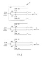
- FIG. 2 shows circuitry of an analog dark-signal averaging (dark average) circuit for an image sensor according to one embodiment of the present invention
- FIG. 3A shows a timing diagram of corresponding signals in FIG. 2 ;
- FIG. 3B is a flow diagram illustrative of the steps of an analog dark-signal averaging method according to the embodiment of the present invention.
- FIG. 2 shows circuitry of an analog dark-signal averaging (dark average) circuit 10 for an image sensor according to one embodiment of the present invention.
- the transistors (or the switches) and the associated control signals use the same reference characters.
- FIG. 3A shows a timing diagram of corresponding signals in FIG. 2
- FIG. 3B is a flow diagram illustrative of the steps of an analog dark-signal averaging method according to the embodiment of the present invention.
- the disclosed analog dark-signal averaging circuit 10 may be generally applied to a digital image processing device, such as, but not limited to, a camera or camcorder.
- the image sensor is a semiconductor based image sensor, such as, but not limited to, a charge-coupled device (CCD) or a complementary metal-oxide-semiconductor (CMOS) sensor, using, for example, pixel circuits to convert images of visible light into electronic signals.
- CCD charge-coupled device
- CMOS complementary metal-oxide-semiconductor
- the dark-signal averaging circuit 10 includes a number of sub-circuits 100 (three representative sub-circuits of which are shown in the figure), each correspondingly inputting a signal from one of the pixel circuits of the image sensor.
- the signals are amplified, for example, by a column amplifier (CA) before entering into the dark-signal averaging circuit 10 .
- the outputs of the dark-signal averaging circuit 10 are ordinarily amplified by a following amplifier, such as a programmable gain amplifier (PGA), which is usually followed by digital circuitry, such as an analog-to-digital converter (ADC) and/or digital signal processor.
- PGA programmable gain amplifier
- ADC analog-to-digital converter
- the circuit 10 is thus named as an “analog” dark-signal averaging circuit.
- each sub-circuit 100 includes a correlated double sampling (CDS) circuit, which includes a sample-and-hold-reset_signal (SHR) switch controlled under a SHR control signal and a sample-and-hold-image_signal (SHS) switch controlled under a SHS control signal.
- the SHR switch and the SHS switch are coupled to a SHR capacitor C SHR and a SHS capacitor C SHS respectively.
- the SHR capacitors C SHR of all (or some) sub-circuits 100 of the analog dark-signal averaging circuit 10 are electrically coupled through average switches DARK_AVG, which are controlled under dark-average control signal (DARK_AVG).
- the interconnecting nodes between the SHR switches and the SHR capacitors C SHR are controllably communicated to each other. Accordingly, the SHR capacitors C SHR of all (or some) sub-circuits 100 are electrically coupled when the average switches DARK_AVG are closed.
- the term “electrically coupled” means that nodes or elements are directly connected by a conductive wire, or are indirectly connected through other electronic elements.
- the SHS capacitors C SHS of all (or some) sub-circuits 100 of the analog dark-signal averaging circuit 10 are also electrically coupled through average switches DARK_AVG, which are controlled under dark-average control signal (DARK_AVG).
- the interconnecting nodes between the SHS switches and the SHS capacitors C SHS are controllably communicated to each other. Accordingly, the SHS capacitors C SHS of all (or some) sub-circuits 100 are electrically coupled when the average switches DARK_AVG are closed.
- the SHR switch is closed such that the reset signal of light-shielded or black pixel(s) is sampled and held in the SHR capacitor C SHR (in step 31 ).
- the SHS switch is closed such that the image signal of the light-shielded pixel(s) is sampled and held in the SHS capacitor C SHS (in step 32 ). It is noted that the overlapping duration of the asserted SHR signal and the asserted SHS signal during t 1 and t 2 is in practice arranged to prevent a coupling effect in one embodiment.
- the SHS signal may be de-asserted during t 1 and t 2 .
- the dark-average control signal closes all average switches DARK_AVG, for example, during t 4 -t 5 in FIG. 3A .
- the SHR capacitors C SHR of all sub-circuits 100 are electrically coupled together, thereby averaging all black pixel reset signals stored on the SHR capacitors C SHR .
- the SHS capacitors C SHS of all sub-circuits 100 are electrically coupled together, thereby averaging all black pixel image signals stored on the SHS capacitors C SHS .
- an average black or dark signal (level) may be obtained within a few clock cycles in the analog domain, in a way faster than the digital domain counterpart. Furthermore, the impact of the fault pixel or pixels (such as hot pixels) on the BLC can be substantially reduced through the analog dark-signal averaging circuit 10 and method of the present embodiment.
Landscapes
- Engineering & Computer Science (AREA)
- Multimedia (AREA)
- Signal Processing (AREA)
- Transforming Light Signals Into Electric Signals (AREA)
Abstract
Description
Claims (7)
Priority Applications (1)
| Application Number | Priority Date | Filing Date | Title |
|---|---|---|---|
| US12/425,341 US8106975B2 (en) | 2009-04-16 | 2009-04-16 | Analog dark average circuit and method for an image sensor |
Applications Claiming Priority (1)
| Application Number | Priority Date | Filing Date | Title |
|---|---|---|---|
| US12/425,341 US8106975B2 (en) | 2009-04-16 | 2009-04-16 | Analog dark average circuit and method for an image sensor |
Publications (2)
| Publication Number | Publication Date |
|---|---|
| US20100265368A1 US20100265368A1 (en) | 2010-10-21 |
| US8106975B2 true US8106975B2 (en) | 2012-01-31 |
Family
ID=42980723
Family Applications (1)
| Application Number | Title | Priority Date | Filing Date |
|---|---|---|---|
| US12/425,341 Expired - Fee Related US8106975B2 (en) | 2009-04-16 | 2009-04-16 | Analog dark average circuit and method for an image sensor |
Country Status (1)
| Country | Link |
|---|---|
| US (1) | US8106975B2 (en) |
Cited By (2)
| Publication number | Priority date | Publication date | Assignee | Title |
|---|---|---|---|---|
| US20110211100A1 (en) * | 2010-02-28 | 2011-09-01 | Ping-Hung Yin | Signel processing circuit capable of selectively adjusting gain factor of sample-and-hold circuit and signal processing method thereof |
| US11653112B2 (en) | 2020-11-23 | 2023-05-16 | Raytheon Company | Analog voting with outlier suppression |
Families Citing this family (2)
| Publication number | Priority date | Publication date | Assignee | Title |
|---|---|---|---|---|
| US20100252717A1 (en) * | 2008-09-29 | 2010-10-07 | Benoit Dupont | Active-pixel sensor |
| US8405747B2 (en) | 2011-02-17 | 2013-03-26 | Omnivision Technologies, Inc. | Analog row black level calibration for CMOS image sensor |
Citations (2)
| Publication number | Priority date | Publication date | Assignee | Title |
|---|---|---|---|---|
| US20050195645A1 (en) * | 1998-03-09 | 2005-09-08 | Roger Panicacci | Readout circuit with gain and analog-to-digital conversion for image sensor |
| US20070063128A1 (en) * | 2003-11-13 | 2007-03-22 | Alexander Krymski | Method and apparatus for pixel signal binning and interpolation in column circuits of a sensor circuit |
-
2009
- 2009-04-16 US US12/425,341 patent/US8106975B2/en not_active Expired - Fee Related
Patent Citations (2)
| Publication number | Priority date | Publication date | Assignee | Title |
|---|---|---|---|---|
| US20050195645A1 (en) * | 1998-03-09 | 2005-09-08 | Roger Panicacci | Readout circuit with gain and analog-to-digital conversion for image sensor |
| US20070063128A1 (en) * | 2003-11-13 | 2007-03-22 | Alexander Krymski | Method and apparatus for pixel signal binning and interpolation in column circuits of a sensor circuit |
Cited By (3)
| Publication number | Priority date | Publication date | Assignee | Title |
|---|---|---|---|---|
| US20110211100A1 (en) * | 2010-02-28 | 2011-09-01 | Ping-Hung Yin | Signel processing circuit capable of selectively adjusting gain factor of sample-and-hold circuit and signal processing method thereof |
| US9083889B2 (en) * | 2010-02-28 | 2015-07-14 | Himax Imaging, Inc. | Signal processing circuit capable of selectively adjusting gain factor of sample-and-hold circuit and signal processing method thereof |
| US11653112B2 (en) | 2020-11-23 | 2023-05-16 | Raytheon Company | Analog voting with outlier suppression |
Also Published As
| Publication number | Publication date |
|---|---|
| US20100265368A1 (en) | 2010-10-21 |
Similar Documents
| Publication | Publication Date | Title |
|---|---|---|
| US10313613B2 (en) | High dynamic range image sensors with flicker and fixed pattern noise mitigation | |
| CN100438585C (en) | Solid-state imaging device | |
| CN104335573B (en) | CMOS image sensor and its method | |
| US7920193B2 (en) | Methods, systems and apparatuses using barrier self-calibration for high dynamic range imagers | |
| EP2037668B1 (en) | Image sensor apparatus and method for improved dynamic range with multiple readout circuit paths | |
| JP4862473B2 (en) | Solid-state imaging device, driving method of solid-state imaging device, and imaging device | |
| US8149310B2 (en) | Readout system and method for an image sensor | |
| US8077227B2 (en) | Method and apparatus providing analog row noise correction and hot pixel filtering | |
| JP5223953B2 (en) | Solid-state imaging device, driving method of solid-state imaging device, and imaging device | |
| US8072526B2 (en) | Image sensor, imaging system, and image sensor control method | |
| US20040090547A1 (en) | Image sensing apparatus | |
| JP2010114487A (en) | Solid-state image pickup apparatus and image pickup apparatus | |
| Lee et al. | On-chip FPN calibration for a linear-logarithmic APS using two-step charge transfer | |
| JP5265249B2 (en) | Imaging device | |
| US8106975B2 (en) | Analog dark average circuit and method for an image sensor | |
| US7991239B2 (en) | Methods, systems and apparatuses for imager row-wise noise correction | |
| US10104321B1 (en) | Image processing system and method for an image sensor | |
| JP4380403B2 (en) | Solid-state imaging device and driving method of solid-state imaging device | |
| US8144224B2 (en) | Binning circuit and method for an image sensor | |
| US10764519B2 (en) | System and method for high dynamic range digital double sampling | |
| JP2007097127A (en) | Solid-state imaging device | |
| JP2012070056A (en) | Imaging device | |
| JP4175100B2 (en) | Signal processing circuit and signal processing method | |
| TWI386051B (en) | Analog dark average circuit and method for an image sensor | |
| JP5737924B2 (en) | Imaging device |
Legal Events
| Date | Code | Title | Description |
|---|---|---|---|
| AS | Assignment |
Owner name: HIMAX IMAGING, INC., CAYMAN ISLANDS Free format text: ASSIGNMENT OF ASSIGNORS INTEREST;ASSIGNOR:YIN, PING-HUNG;REEL/FRAME:022557/0908 Effective date: 20090401 |
|
| ZAAA | Notice of allowance and fees due |
Free format text: ORIGINAL CODE: NOA |
|
| ZAAB | Notice of allowance mailed |
Free format text: ORIGINAL CODE: MN/=. |
|
| STCF | Information on status: patent grant |
Free format text: PATENTED CASE |
|
| FPAY | Fee payment |
Year of fee payment: 4 |
|
| MAFP | Maintenance fee payment |
Free format text: PAYMENT OF MAINTENANCE FEE, 8TH YEAR, LARGE ENTITY (ORIGINAL EVENT CODE: M1552); ENTITY STATUS OF PATENT OWNER: LARGE ENTITY Year of fee payment: 8 |
|
| FEPP | Fee payment procedure |
Free format text: MAINTENANCE FEE REMINDER MAILED (ORIGINAL EVENT CODE: REM.); ENTITY STATUS OF PATENT OWNER: LARGE ENTITY |
|
| LAPS | Lapse for failure to pay maintenance fees |
Free format text: PATENT EXPIRED FOR FAILURE TO PAY MAINTENANCE FEES (ORIGINAL EVENT CODE: EXP.); ENTITY STATUS OF PATENT OWNER: LARGE ENTITY |
|
| STCH | Information on status: patent discontinuation |
Free format text: PATENT EXPIRED DUE TO NONPAYMENT OF MAINTENANCE FEES UNDER 37 CFR 1.362 |
|
| FP | Lapsed due to failure to pay maintenance fee |
Effective date: 20240131 |