EP1684334B1 - Verfahren und System zur Beschichtung und zur Entwicklung eines Films - Google Patents
Verfahren und System zur Beschichtung und zur Entwicklung eines Films Download PDFInfo
- Publication number
- EP1684334B1 EP1684334B1 EP06001221A EP06001221A EP1684334B1 EP 1684334 B1 EP1684334 B1 EP 1684334B1 EP 06001221 A EP06001221 A EP 06001221A EP 06001221 A EP06001221 A EP 06001221A EP 1684334 B1 EP1684334 B1 EP 1684334B1
- Authority
- EP
- European Patent Office
- Prior art keywords
- substrate
- unit
- block
- wafer
- developing
- Prior art date
- Legal status (The legal status is an assumption and is not a legal conclusion. Google has not performed a legal analysis and makes no representation as to the accuracy of the status listed.)
- Active
Links
- 238000000034 method Methods 0.000 title claims description 198
- 239000007888 film coating Substances 0.000 title 2
- 238000009501 film coating Methods 0.000 title 2
- 238000012546 transfer Methods 0.000 claims description 283
- 239000000758 substrate Substances 0.000 claims description 246
- 238000012545 processing Methods 0.000 claims description 204
- 230000008569 process Effects 0.000 claims description 182
- 238000000576 coating method Methods 0.000 claims description 153
- 239000007788 liquid Substances 0.000 claims description 152
- 239000011248 coating agent Substances 0.000 claims description 151
- 238000004140 cleaning Methods 0.000 claims description 110
- 230000001681 protective effect Effects 0.000 claims description 107
- 238000010438 heat treatment Methods 0.000 claims description 77
- 239000000126 substance Substances 0.000 claims description 63
- 238000001816 cooling Methods 0.000 claims description 53
- 238000007654 immersion Methods 0.000 claims description 45
- 101150075071 TRS1 gene Proteins 0.000 claims description 23
- 239000005871 repellent Substances 0.000 claims description 19
- 230000007547 defect Effects 0.000 claims description 18
- 239000002245 particle Substances 0.000 claims description 12
- 101000588012 Homo sapiens SREBP regulating gene protein Proteins 0.000 claims description 11
- 102100031580 SREBP regulating gene protein Human genes 0.000 claims description 11
- 101100328883 Arabidopsis thaliana COL1 gene Proteins 0.000 claims description 8
- 238000011161 development Methods 0.000 claims description 7
- 101100328893 Arabidopsis thaliana COL5 gene Proteins 0.000 claims description 5
- 102100031077 Calcineurin B homologous protein 3 Human genes 0.000 claims description 5
- 101000777270 Homo sapiens Calcineurin B homologous protein 3 Proteins 0.000 claims description 5
- 230000001788 irregular Effects 0.000 claims description 2
- -1 POST2 Proteins 0.000 claims 1
- 235000012431 wafers Nutrition 0.000 description 438
- 230000007246 mechanism Effects 0.000 description 22
- 238000007689 inspection Methods 0.000 description 19
- YVGGHNCTFXOJCH-UHFFFAOYSA-N DDT Chemical compound C1=CC(Cl)=CC=C1C(C(Cl)(Cl)Cl)C1=CC=C(Cl)C=C1 YVGGHNCTFXOJCH-UHFFFAOYSA-N 0.000 description 12
- 101710189714 Major cell-binding factor Proteins 0.000 description 12
- 238000010276 construction Methods 0.000 description 11
- 238000004519 manufacturing process Methods 0.000 description 11
- 239000012530 fluid Substances 0.000 description 8
- 230000002093 peripheral effect Effects 0.000 description 8
- 229910052751 metal Inorganic materials 0.000 description 7
- 239000002184 metal Substances 0.000 description 7
- 101100182770 Streptococcus phage Cp-7 CPL7 gene Proteins 0.000 description 6
- 229910052782 aluminium Inorganic materials 0.000 description 5
- XAGFODPZIPBFFR-UHFFFAOYSA-N aluminium Chemical compound [Al] XAGFODPZIPBFFR-UHFFFAOYSA-N 0.000 description 5
- 238000009833 condensation Methods 0.000 description 5
- 230000005494 condensation Effects 0.000 description 5
- 230000001965 increasing effect Effects 0.000 description 5
- 238000009834 vaporization Methods 0.000 description 5
- 230000008016 vaporization Effects 0.000 description 5
- 101100221835 Arabidopsis thaliana CPL2 gene Proteins 0.000 description 4
- 101150016835 CPL1 gene Proteins 0.000 description 4
- 101100468774 Saccharomyces cerevisiae (strain ATCC 204508 / S288c) RIM13 gene Proteins 0.000 description 4
- 101100182771 Streptococcus phage Cp-9 CPL9 gene Proteins 0.000 description 4
- 239000004065 semiconductor Substances 0.000 description 4
- XLYOFNOQVPJJNP-UHFFFAOYSA-N water Substances O XLYOFNOQVPJJNP-UHFFFAOYSA-N 0.000 description 4
- 101100221837 Arabidopsis thaliana CPL4 gene Proteins 0.000 description 3
- 101100221838 Arabidopsis thaliana CPL5 gene Proteins 0.000 description 3
- 101100536545 Arabidopsis thaliana TCL2 gene Proteins 0.000 description 3
- 238000013461 design Methods 0.000 description 3
- 238000003756 stirring Methods 0.000 description 3
- RYGMFSIKBFXOCR-UHFFFAOYSA-N Copper Chemical compound [Cu] RYGMFSIKBFXOCR-UHFFFAOYSA-N 0.000 description 2
- UFWIBTONFRDIAS-UHFFFAOYSA-N Naphthalene Chemical compound C1=CC=CC2=CC=CC=C21 UFWIBTONFRDIAS-UHFFFAOYSA-N 0.000 description 2
- 230000002411 adverse Effects 0.000 description 2
- 230000008901 benefit Effects 0.000 description 2
- 239000000969 carrier Substances 0.000 description 2
- 229910052802 copper Inorganic materials 0.000 description 2
- 239000010949 copper Substances 0.000 description 2
- 208000002925 dental caries Diseases 0.000 description 2
- 230000000694 effects Effects 0.000 description 2
- 239000011521 glass Substances 0.000 description 2
- 239000004973 liquid crystal related substance Substances 0.000 description 2
- 239000000463 material Substances 0.000 description 2
- NBRQRXRBIHVLGI-OWXODZSWSA-N (4as,5ar,12ar)-1,10,11,12a-tetrahydroxy-3,12-dioxo-4a,5,5a,6-tetrahydro-4h-tetracene-2-carboxamide Chemical compound C1C2=CC=CC(O)=C2C(O)=C(C2=O)[C@@H]1C[C@@H]1[C@@]2(O)C(O)=C(C(=O)N)C(=O)C1 NBRQRXRBIHVLGI-OWXODZSWSA-N 0.000 description 1
- 101100328890 Arabidopsis thaliana COL3 gene Proteins 0.000 description 1
- 229910001111 Fine metal Inorganic materials 0.000 description 1
- DGAQECJNVWCQMB-PUAWFVPOSA-M Ilexoside XXIX Chemical compound C[C@@H]1CC[C@@]2(CC[C@@]3(C(=CC[C@H]4[C@]3(CC[C@@H]5[C@@]4(CC[C@@H](C5(C)C)OS(=O)(=O)[O-])C)C)[C@@H]2[C@]1(C)O)C)C(=O)O[C@H]6[C@@H]([C@H]([C@@H]([C@H](O6)CO)O)O)O.[Na+] DGAQECJNVWCQMB-PUAWFVPOSA-M 0.000 description 1
- 238000010521 absorption reaction Methods 0.000 description 1
- 230000015572 biosynthetic process Effects 0.000 description 1
- 230000008859 change Effects 0.000 description 1
- 239000000356 contaminant Substances 0.000 description 1
- 230000002950 deficient Effects 0.000 description 1
- 230000001419 dependent effect Effects 0.000 description 1
- 238000007599 discharging Methods 0.000 description 1
- 238000009826 distribution Methods 0.000 description 1
- 239000000428 dust Substances 0.000 description 1
- 230000002708 enhancing effect Effects 0.000 description 1
- FFUAGWLWBBFQJT-UHFFFAOYSA-N hexamethyldisilazane Chemical compound C[Si](C)(C)N[Si](C)(C)C FFUAGWLWBBFQJT-UHFFFAOYSA-N 0.000 description 1
- 238000009434 installation Methods 0.000 description 1
- 239000000155 melt Substances 0.000 description 1
- 230000035515 penetration Effects 0.000 description 1
- 238000007789 sealing Methods 0.000 description 1
- 229910052708 sodium Inorganic materials 0.000 description 1
- 239000011734 sodium Substances 0.000 description 1
- 239000002904 solvent Substances 0.000 description 1
- 229910001220 stainless steel Inorganic materials 0.000 description 1
- 239000010935 stainless steel Substances 0.000 description 1
- 230000026676 system process Effects 0.000 description 1
- 238000004148 unit process Methods 0.000 description 1
- 238000009736 wetting Methods 0.000 description 1
Images


Classifications
-
- G—PHYSICS
- G03—PHOTOGRAPHY; CINEMATOGRAPHY; ANALOGOUS TECHNIQUES USING WAVES OTHER THAN OPTICAL WAVES; ELECTROGRAPHY; HOLOGRAPHY
- G03F—PHOTOMECHANICAL PRODUCTION OF TEXTURED OR PATTERNED SURFACES, e.g. FOR PRINTING, FOR PROCESSING OF SEMICONDUCTOR DEVICES; MATERIALS THEREFOR; ORIGINALS THEREFOR; APPARATUS SPECIALLY ADAPTED THEREFOR
- G03F7/00—Photomechanical, e.g. photolithographic, production of textured or patterned surfaces, e.g. printing surfaces; Materials therefor, e.g. comprising photoresists; Apparatus specially adapted therefor
- G03F7/16—Coating processes; Apparatus therefor
-
- G—PHYSICS
- G03—PHOTOGRAPHY; CINEMATOGRAPHY; ANALOGOUS TECHNIQUES USING WAVES OTHER THAN OPTICAL WAVES; ELECTROGRAPHY; HOLOGRAPHY
- G03F—PHOTOMECHANICAL PRODUCTION OF TEXTURED OR PATTERNED SURFACES, e.g. FOR PRINTING, FOR PROCESSING OF SEMICONDUCTOR DEVICES; MATERIALS THEREFOR; ORIGINALS THEREFOR; APPARATUS SPECIALLY ADAPTED THEREFOR
- G03F7/00—Photomechanical, e.g. photolithographic, production of textured or patterned surfaces, e.g. printing surfaces; Materials therefor, e.g. comprising photoresists; Apparatus specially adapted therefor
- G03F7/26—Processing photosensitive materials; Apparatus therefor
- G03F7/265—Selective reaction with inorganic or organometallic reagents after image-wise exposure, e.g. silylation
-
- H—ELECTRICITY
- H01—ELECTRIC ELEMENTS
- H01L—SEMICONDUCTOR DEVICES NOT COVERED BY CLASS H10
- H01L21/00—Processes or apparatus adapted for the manufacture or treatment of semiconductor or solid state devices or of parts thereof
- H01L21/02—Manufacture or treatment of semiconductor devices or of parts thereof
- H01L21/027—Making masks on semiconductor bodies for further photolithographic processing not provided for in group H01L21/18 or H01L21/34
- H01L21/0271—Making masks on semiconductor bodies for further photolithographic processing not provided for in group H01L21/18 or H01L21/34 comprising organic layers
- H01L21/0273—Making masks on semiconductor bodies for further photolithographic processing not provided for in group H01L21/18 or H01L21/34 comprising organic layers characterised by the treatment of photoresist layers
-
- H—ELECTRICITY
- H01—ELECTRIC ELEMENTS
- H01L—SEMICONDUCTOR DEVICES NOT COVERED BY CLASS H10
- H01L21/00—Processes or apparatus adapted for the manufacture or treatment of semiconductor or solid state devices or of parts thereof
- H01L21/67—Apparatus specially adapted for handling semiconductor or electric solid state devices during manufacture or treatment thereof; Apparatus specially adapted for handling wafers during manufacture or treatment of semiconductor or electric solid state devices or components ; Apparatus not specifically provided for elsewhere
- H01L21/67005—Apparatus not specifically provided for elsewhere
- H01L21/67011—Apparatus for manufacture or treatment
- H01L21/6715—Apparatus for applying a liquid, a resin, an ink or the like
-
- G—PHYSICS
- G03—PHOTOGRAPHY; CINEMATOGRAPHY; ANALOGOUS TECHNIQUES USING WAVES OTHER THAN OPTICAL WAVES; ELECTROGRAPHY; HOLOGRAPHY
- G03F—PHOTOMECHANICAL PRODUCTION OF TEXTURED OR PATTERNED SURFACES, e.g. FOR PRINTING, FOR PROCESSING OF SEMICONDUCTOR DEVICES; MATERIALS THEREFOR; ORIGINALS THEREFOR; APPARATUS SPECIALLY ADAPTED THEREFOR
- G03F7/00—Photomechanical, e.g. photolithographic, production of textured or patterned surfaces, e.g. printing surfaces; Materials therefor, e.g. comprising photoresists; Apparatus specially adapted therefor
- G03F7/16—Coating processes; Apparatus therefor
- G03F7/168—Finishing the coated layer, e.g. drying, baking, soaking
-
- G—PHYSICS
- G03—PHOTOGRAPHY; CINEMATOGRAPHY; ANALOGOUS TECHNIQUES USING WAVES OTHER THAN OPTICAL WAVES; ELECTROGRAPHY; HOLOGRAPHY
- G03F—PHOTOMECHANICAL PRODUCTION OF TEXTURED OR PATTERNED SURFACES, e.g. FOR PRINTING, FOR PROCESSING OF SEMICONDUCTOR DEVICES; MATERIALS THEREFOR; ORIGINALS THEREFOR; APPARATUS SPECIALLY ADAPTED THEREFOR
- G03F7/00—Photomechanical, e.g. photolithographic, production of textured or patterned surfaces, e.g. printing surfaces; Materials therefor, e.g. comprising photoresists; Apparatus specially adapted therefor
- G03F7/26—Processing photosensitive materials; Apparatus therefor
- G03F7/30—Imagewise removal using liquid means
- G03F7/3042—Imagewise removal using liquid means from printing plates transported horizontally through the processing stations
-
- G—PHYSICS
- G03—PHOTOGRAPHY; CINEMATOGRAPHY; ANALOGOUS TECHNIQUES USING WAVES OTHER THAN OPTICAL WAVES; ELECTROGRAPHY; HOLOGRAPHY
- G03F—PHOTOMECHANICAL PRODUCTION OF TEXTURED OR PATTERNED SURFACES, e.g. FOR PRINTING, FOR PROCESSING OF SEMICONDUCTOR DEVICES; MATERIALS THEREFOR; ORIGINALS THEREFOR; APPARATUS SPECIALLY ADAPTED THEREFOR
- G03F7/00—Photomechanical, e.g. photolithographic, production of textured or patterned surfaces, e.g. printing surfaces; Materials therefor, e.g. comprising photoresists; Apparatus specially adapted therefor
- G03F7/70—Microphotolithographic exposure; Apparatus therefor
- G03F7/70691—Handling of masks or workpieces
- G03F7/70716—Stages
-
- H—ELECTRICITY
- H01—ELECTRIC ELEMENTS
- H01L—SEMICONDUCTOR DEVICES NOT COVERED BY CLASS H10
- H01L21/00—Processes or apparatus adapted for the manufacture or treatment of semiconductor or solid state devices or of parts thereof
-
- H—ELECTRICITY
- H01—ELECTRIC ELEMENTS
- H01L—SEMICONDUCTOR DEVICES NOT COVERED BY CLASS H10
- H01L21/00—Processes or apparatus adapted for the manufacture or treatment of semiconductor or solid state devices or of parts thereof
- H01L21/02—Manufacture or treatment of semiconductor devices or of parts thereof
- H01L21/027—Making masks on semiconductor bodies for further photolithographic processing not provided for in group H01L21/18 or H01L21/34
- H01L21/0271—Making masks on semiconductor bodies for further photolithographic processing not provided for in group H01L21/18 or H01L21/34 comprising organic layers
- H01L21/0273—Making masks on semiconductor bodies for further photolithographic processing not provided for in group H01L21/18 or H01L21/34 comprising organic layers characterised by the treatment of photoresist layers
- H01L21/0274—Photolithographic processes
-
- H—ELECTRICITY
- H01—ELECTRIC ELEMENTS
- H01L—SEMICONDUCTOR DEVICES NOT COVERED BY CLASS H10
- H01L21/00—Processes or apparatus adapted for the manufacture or treatment of semiconductor or solid state devices or of parts thereof
- H01L21/67—Apparatus specially adapted for handling semiconductor or electric solid state devices during manufacture or treatment thereof; Apparatus specially adapted for handling wafers during manufacture or treatment of semiconductor or electric solid state devices or components ; Apparatus not specifically provided for elsewhere
- H01L21/67005—Apparatus not specifically provided for elsewhere
- H01L21/67011—Apparatus for manufacture or treatment
- H01L21/67155—Apparatus for manufacturing or treating in a plurality of work-stations
- H01L21/67161—Apparatus for manufacturing or treating in a plurality of work-stations characterized by the layout of the process chambers
- H01L21/67178—Apparatus for manufacturing or treating in a plurality of work-stations characterized by the layout of the process chambers vertical arrangement
-
- H—ELECTRICITY
- H01—ELECTRIC ELEMENTS
- H01L—SEMICONDUCTOR DEVICES NOT COVERED BY CLASS H10
- H01L21/00—Processes or apparatus adapted for the manufacture or treatment of semiconductor or solid state devices or of parts thereof
- H01L21/67—Apparatus specially adapted for handling semiconductor or electric solid state devices during manufacture or treatment thereof; Apparatus specially adapted for handling wafers during manufacture or treatment of semiconductor or electric solid state devices or components ; Apparatus not specifically provided for elsewhere
- H01L21/67005—Apparatus not specifically provided for elsewhere
- H01L21/67011—Apparatus for manufacture or treatment
- H01L21/67155—Apparatus for manufacturing or treating in a plurality of work-stations
- H01L21/67184—Apparatus for manufacturing or treating in a plurality of work-stations characterized by the presence of more than one transfer chamber
-
- H—ELECTRICITY
- H01—ELECTRIC ELEMENTS
- H01L—SEMICONDUCTOR DEVICES NOT COVERED BY CLASS H10
- H01L21/00—Processes or apparatus adapted for the manufacture or treatment of semiconductor or solid state devices or of parts thereof
- H01L21/67—Apparatus specially adapted for handling semiconductor or electric solid state devices during manufacture or treatment thereof; Apparatus specially adapted for handling wafers during manufacture or treatment of semiconductor or electric solid state devices or components ; Apparatus not specifically provided for elsewhere
- H01L21/67005—Apparatus not specifically provided for elsewhere
- H01L21/67011—Apparatus for manufacture or treatment
- H01L21/67155—Apparatus for manufacturing or treating in a plurality of work-stations
- H01L21/6719—Apparatus for manufacturing or treating in a plurality of work-stations characterized by the construction of the processing chambers, e.g. modular processing chambers
Definitions
- the present invention relates to a coating and developing system for applying a liquid resist to a surface of a substrate, such as a semiconductor wafer or a LCD substrate, namely, a glass substrate for a liquid crystal display, to coat the surface with a resist film and developing the exposed resist film, and a coating and developing method.
- a substrate such as a semiconductor wafer or a LCD substrate, namely, a glass substrate for a liquid crystal display
- a resist pattern forming system built by combining an exposure system with a coating and developing system.
- Fig 23 shows a known resist pattern forming system of this type disclosed in, for example, JP 2004-193597 A .
- a carrier 10 holding a plurality of wafers W is delivered onto a carrier stage 11 installed in a carrier handling block 1A, and then a transfer arm 12 transfers the wafer W from the carrier 10 to a processing block 1B.
- the wafer W is delivered to a coating unit 13A installed in the processing block 1B.
- the coating unit 13A applies a liquid resist to a surface of the wafer W in a resist film.
- the wafer coated with the resist film is carried via an interface block 1C to an exposure system 1D.
- Resist films of different types are formed in different coating mode, respectively.
- a first coating mode forms a resist film and antireflection films over and under the resist film
- a second coating mode forms a resist film and an antireflection film over or under the resist film
- a third coating mode forms only a resist film. Therefore, in some cases, the units necessary for forming films, such as the coating unit, the heating unit and the cooling unit, processes wafers of different lots under different processing conditions. In such a case, a complex carrying program must be prepared for each type of the resist film when the coating unit, the heating unit and the cooling unit are installed in the same processing block because the different types of resist films are formed by using different units and are carried along different carrying paths. Since carrying programs to be produced according to the carrying schedule are originally complex, work for producing a carrying program for each of desired resist films is very complex and troublesome and such work is practically impossible.
- the processing block is inevitably large and occupies a large area.
- a recent exposure system operates at a high throughput. Consequently, the coating and developing system is required to have a high processing ability corresponding to the throughput of the exposure system.
- the same carrying system operates to carry a wafer W to the coating unit for forming a resist film before the exposure process, to carry a wafer to an antireflection film forming unit for forming the antireflection film and to carry a wafer coated with an exposed resist film to the developing unit after exposure, it is difficult to operate the exposure system at a high throughput.
- the temperature adjusting unit includes a first temperature adjusting plate for supporting, for example, a substrate heated by a heating unit and for roughly adjusting the temperature of the substrate to a first temperature, and a second temperature adjusting plate for supporting a substrate and for precisely adjusting the temperature of the substrate.
- the coating and developing system carries out a coating and developing method including the steps of: selecting one of a first carrying mode in which a substrate is carried to all the film forming unit blocks, a second carrying mode in which a substrate is carried to the liquid resist applying unit block and to a liquid-processing unit block for forming an antireflection film before a resist film is formed on a substrate, and a third carrying mode in which a substrate is carried to the liquid resist applying unit block for applying a liquid resist to the substrate and to the liquid-processing unit block for applying a chemical solution for forming an antireflection film to the substrate after the liquid resist has been applied to the substrate; forming films on the substrate by carrying the substrate from one to another of the film forming unit blocks in the selected carrying mode; and subjecting the substrate coated with the films and processed by an exposure process to a developing process by a developing unit block in a layer other than layers including the plurality of film forming unit blocks.
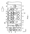
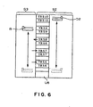
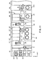
- the processing block S2 surrounded by a casing 24 is connected to the back end of the carrier handling block S1.
- the processing block S2 includes a first unit block (first DEV layer) B1 for carrying out a developing process, a second unit block (second DEV layer) B2 for carrying out a developing process, a third unit block (TCT layer) B3 for carrying out an antireflection film forming process for forming a second antireflection film over a resist film, a fourth unit block (COT layer) B4 for carrying out a liquid resist applying process, and a fifth unit block (BCT layer) B5 for carrying out an antireflection film forming process for forming a first antireflection film under the resist film.
- the unit blocks B1 to B5 are arranged vertically upward in that order.
- the DEV layers B1 and B2 are developing unit blocks
- the TCT layer B3, the COT layer B4 and the BCT layer B5 are film forming unit blocks.
- a local area, contiguous with the carrier handling block S1, of the carrying area R1 is a first transfer area R2.
- the shelf unit U5 is disposed in the transfer area R2 such that the transfer arm C and the main arm A4 are able to gain access to the shelf unit U5.
- a first transfer arm D1, namely, a first transfer means, is disposed in the first transfer area R2 to deliver the wafer W to and to receive the wafer W from the shelf unit U5.
- the first transfer arm D1 and the second transfer arm D2 are similar in construction to the interface arm B, except that the first transfer arm D1 and the second transfer arm D2 are not turnable about a vertical axis.
- the respective operations of the first transfer arm D, the second transfer arm D2 and the interface arm B are controlled by a controller, not shown, on the basis of instructions provided by the control unit 6.
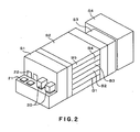
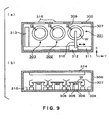
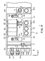
- the coating unit 31 will be briefly described in connection with Fig. 9 .
- the coating unit 31 is provided with three coating devices 301, 302 and 303 placed in a processing vessel 300.
- the processing devices 301 to 303 are arranged on a base 304 along the Y-axis so as to face the carrying area R1.
- the developing unit 32 is substantially similar to the coating unit 31, except that the developing unit 32 has a developer supply area extending along the length of a developer supply nozzle for pouring a developer in a direction parallel to the diameter of the wafer W, and is provided with a cleaning liquid pouring nozzle.
- a plurality of developing devices are disposed in the common processing vessel 300.
- the cleaning liquid pouring nozzle is similar to the chemical solution supply nozzle 310 and can be moved along the guide rail 311 and can be vertically moved by a moving mechanism.
- the cleaning liquid pouring nozzle pours a cleaning liquid onto the wafers W held on the spin chucks 305 of the coating devices 301 to 303.
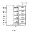
- the interface arm B carries the wafer W from the second transfer stage TRS8 to the exposure system S4 to subject the wafer W to a predetermined exposure process.
- the interface arm B carries the wafer W to the second transfer stage TRS6 (TRS7) of the shelf unit U6 to deliver the wafer W to the DEV layer B1 (DEV layer B2).
- the main arm A1 (main arm A2) carries the wafer W from the second transfer stage TRS6 (TRS7) to the heating unit PEB1 (PEB2), the cooling unit COL1 (COL2), the developing unit 32, the heating unit POST1 (POST2) of the DEV layer B1 (DEV layer B2) to process the wafer W by a predetermined developing process.
- the wafer is delivered to the first transfer stage TRS1 (TRS2).
- the transfer arm C carries the wafer W to return the wafer W to the carrier 20 placed on the carrier support table 21 of the carrier handling block S1.
- the resist pattern forming system is provided with the control unit 6 including a computer for managing recipes for the operations of the processing units, managing carrying recipes for carrying the wafer W along carrying routes and controlling the processing operations of the processing units and the operations of the main arms A1 to A5, the transfer arm C, the first transfer arm D1, the second transfer arm D2 and the interface arm B.
- the control unit 6 controls the unit blocks B1 to B5 to carry and process the wafer W.
- Defocus inspection by the defocus inspection device finds out a defocus condition of the exposure system through the comparison of a pattern formed on the wafer W with a registered correct pattern.
- the line width measuring device decides whether or not exposure and exposure time in which the exposure system processed the resist film formed on the wafer W are proper through the comparison of a measured pattern with a previously registered correct pattern.
- the photomask alignment inspecting device decides whether or not exposure and exposure time in which the exposure system processed the resist film formed on the wafer W are proper through the comparison of a pattern of a specific part which can be compared with a pattern of a lower layer with a previously registered correct pattern.
- the interface arm B carries the wafer W processed by the immersion exposure process to the cleaning unit 403, and carries the wafer W from the cleaning unit 403 to the second temperature adjusting plate 520 of the temperature adjusting unit (CPL1).
- the temperature adjusting unit (CPL1) cools the wafer W at 23°C + 0.2°C.
Landscapes
- Engineering & Computer Science (AREA)
- Physics & Mathematics (AREA)
- General Physics & Mathematics (AREA)
- Condensed Matter Physics & Semiconductors (AREA)
- Manufacturing & Machinery (AREA)
- Computer Hardware Design (AREA)
- Microelectronics & Electronic Packaging (AREA)
- Power Engineering (AREA)
- Chemical & Material Sciences (AREA)
- Chemical Kinetics & Catalysis (AREA)
- Inorganic Chemistry (AREA)
- Organic Chemistry (AREA)
- Container, Conveyance, Adherence, Positioning, Of Wafer (AREA)
- Exposure Of Semiconductors, Excluding Electron Or Ion Beam Exposure (AREA)
- Photosensitive Polymer And Photoresist Processing (AREA)
- Coating Apparatus (AREA)
- Non-Silver Salt Photosensitive Materials And Non-Silver Salt Photography (AREA)
Claims (21)
- Beschichtungs- und Entwicklungssystem umfassend:einen Trägerhandhabungsblock (S1) zum Aufnehmen eines Substrates (W), das dorthin durch einen Träger (20) transportiert wird;einen Bearbeitungsblock (S2) zum Bearbeiten eines Substrates, das dorthin von dem Trägerhandhabungsblock transferiert wird, um Filme einschließlich eines Fotolackfilms auf dem Substrat zu bilden; undeinen Anschlussblock (S3) zum Transportieren eines Substrates zu einem Belichtungssystem, zum Aufnehmen eines im Belichtungssystem bearbeiteten Substrates und zur Rückgabe des Substrates an den Bearbeitungsblock (S2) um das Substrat einem Entwicklungsprozess auszusetzen und um das Substrat welches durch den Entwicklungsprozess bearbeitet wurde, zum Trägerhandhabungsblock (S1) zu transferieren, wobeia) der Bearbeitungsblock (S2) mit einer Vielzahl von in Schichten gestapelten Filmbildungseinheitsblöcken (B3, B4, B5), sowie einem bezüglich der Filmbildungseinheitsblöcke in Schichten gestapelten Entwicklungseinheitsblock (B1, B2) versehen ist und dadurch gekennzeichnet, dassb) die Vielzahl von in Schichten gestapelten Filmbildungseinheitsblöcken einen Flüssigfotolackaufbringungseinheitsblock (B4) zur Aufbringung eines flüssigen Fotolackes auf ein Substrat und einen Nassbearbeitungseinheitsblock (B3, B5) zur Aufbringung einer chemischen Lösung auf ein Substrat, um einen antireflektierenden Film zu bilden, umfasst; undc) jeder der Filmbildungseinheitsblöcke und Entwicklungseinheitsblöcke eine Nassbearbeitungseinheit zur Aufbringung einer chemischen Lösung auf ein Substrat, eine Heizeinheit (POST1, POST2, CHP3, CHP4, CHP5) zum Heizen eines Substrates und ein Transportmittel (A1, A2, A3, A4, A5) zum Transport eines Substrates von einer zur anderen der Nassbearbeitungseinheit und der Heizeinheit umfasst.
- Beschichtungs- und Entwicklungssystem gemäß Anspruch 1, bei dem jeder der Einheitsblöcke (B1 bis B5) eine Kühleinheit (COL1 bis COL5) zur Kühlung eines Substrates umfasst.
- Beschichtungs- und Entwicklungssystem gemäß Anspruch 1 weiter umfassend:Transportrezepte, die Substrattransportpfade innerhalb der Einheitsblöcke spezifizieren; undein Moduswahlmittel (6) zur Wahl eines ersten Transportmodus, bei dem ein Substrat zu allen Einheitsblöcken transportiert wird, eines zweiten Transportmodus, bei dem ein Substrat zu einem Flüssigfotolackaufbringungseinheitsblock, einem Nassbearbeitungseinheitsblock zur Bildung eines antireflektierenden Films bevor der flüssige Fotolack auf das Substrat aufgebracht wird, und einem Entwicklungseinheitsblock (32) zur Durchführung eines Entwicklungsprozesses transportiert wird, oder eines dritten Transportmodus, bei dem ein Substrat zu einem Flüssigfotolackaufbringungseinheitsblock, einem Aufbringungseinheitsblock für eine chemische Lösung, zur Aufbringung einer chemischen Lösung zur Bildung eines antireflektierenden Filmes nachdem der flüssige Fotolack auf ein Substrat aufgebracht wurde, und einen Entwicklungseinheitsblock (32) zur Durchführung eines Entwicklungsprozesses, transportiert wird;wobei das Moduswahlmittel (6) die Einheitsblöcke auswählt, zu denen ein Substrat zu transportieren ist, und das Transportrezept für die gewählten Einheitsblöcke wählt, um ein Substrat zu bearbeiten.
- Beschichtungs- und Entwicklungssystem gemäß Anspruch 1 weiter umfassend:eine erste Transferbühnengruppe aus ersten Transferbühnen (TRS1 bis TRS5), die für die Einheitsblöcke in Schichten gestapelt sind, angeordnet an der Seite des Trägerhandhabungsblockes um ein Substrat von den Transportmitteln (A1 bis A5) der jeweiligen Einheitsblöcke zu empfangen und bereitzustellen;eine zweite Transferbühnengruppe aus zweiten Transferbühnen (TRS6 bis TRS9)in Schichten gestapelt und an der Seite des Anschlussblockes (S3) angeordnet, um ein Substrat von den Transportmitteln (A1 bis A5) der jeweiligen Einheitsblöcke zu empfangen und bereitzustellen,ein erstes Substrattransfermittel (D1) zum Transport eines Substrates von einer zur anderen der ersten Transferbühnen;
undein zweites Substrattransfermittel (D2) zum Transport eines Substrates von einer zur anderen der zweiten Transferbühnen. - Beschichtungs- und Entwicklungssystem gemäß Anspruch 4, bei dem die erste Transferbühnengruppe eine Transferbühne für den Trägerhanhabungsblock (S1) umfasst, mittels welchem ein Substrat zwischen dem Trägerhanhabungsblock (S1) und dem Bearbeitungsblock (S2) transportiert wird.
- Beschichtungs- und Entwicklungssystem gemäß Anspruch 4, bei dem die zweite Transferbühnengruppe eine Anschlussblocktransferbühne umfasst, mittels welcher ein Substrat zwischen dem Anschlussblock (S3) und dem Bearbeitungsblock (S2) transportiert wird.
- Beschichtungs- und Entwicklungssystem gemäß Anspruch 1, bei dem die Nassbearbeitungseinheit, umfasst in dem Filmbildungseinheitsblock (B3, B4, B5), eine Vielzahl von lateral angeordneten Substrathaltevorrichtungen, die jeweils zum Halten einer Vielzahl von Substraten vorgesehen sind, angeordnet in einem gemeinsamen Prozessbehälter, und eine gemeinsamen Aufbringungsdüse für eine chemische Lösung zur Aufbringung einer chemischen Lösung auf Substrate aufweist, welche durch die Vielzahl der Substrathaltevorrichtungen gehalten werden.
- Beschichtungs- und Entwicklungssystem gemäß Anspruch 1, bei dem ein mit funktionalen Einheiten (71, 72) versehener Zusatzblock (S5), welcher Prozesse nach einer Filmbildung und vor einem Belichtungsprozess und/oder nach dem Belichtungsprozess und vor dem Entwicklungsprozess und nach dem Entwicklungsprozess ausführt, zwischen dem Bearbeitungsblock (S2) und dem Anschlussblock (S3) eingeschoben ist.
- Beschichtungs- und Entwicklungssystem gemäß Anspruch 8, bei dem die funktionalen Einheiten des Zusatzblocks (S5) zumindest eine der folgenden Einheiten umfassen: eine Filmdickenuntersuchungseinheit zur Untersuchung der Dicke eines auf einem Substrat gebildeten Filmes, eine Reinigungseinheit (403), zur Reinigung eines Substrates vor dem Belichtungsprozess und/oder nach dem Belichtungsprozess, eine Defokussierungsinspektionseinheit zum Auffinden eines im Belichtungssystem auftretend fehlerhaft registrierten Musters, eine Detektionsvorrichtung für irreguläre Beschichtungen zur Detektion von Irregularitäten in einem flüssigen Fotolackfilm, eine Detektionsvorrichtung für fehlerhafte Belichtung zur Detektion von Defekten im entwickelten Film, eine Partikelzählvorrichtung zur Zählung von Partikeln die einem Substrat anheften, eine Detektionsvorrichtung für Kometen zur Detektion von Kometen in einem auf einem Substrat gebildeten Fotolackfilm, eine Detektionsvorrichtung für Rückspritzer zur Detektion von Defekten in der Oberfläche eines Substrates, eine Detektionsvorrichtung für Ablagerungen zur Detektion von restlichen Fotolack der durch einen Entwicklungsprozess auf einem Substrat zurück bleibt, eine Defektdetektionsvorrichtung Detektion von Defekten verursacht durch einen Aufbringungsprozess flüssigen Fotolackes und/oder einen Entwicklungsprozess, eine Linienbreitenmessvorrichtung zum Messen von Linien eines gemusterten Fotolackfilmes gebildet auf einem Substrat, und/oder einer Registeruntersuchungsvorrichtung zur Untersuchung der Register einer Fotomaske auf einem Substrat nach einem Belichtungsprozess.
- Beschichtungs- und Entwicklungssystem gemäß Anspruch 8, bei dem das Belichtungssystem eine flüssige Schicht auf einer Oberfläche eines Substrates zur Immersionsbelichtung bildet, wobei die funktionale Einheit des Zusatzblockes eine Reinigungseinheit (403) zur Reinigung eines durch Immersionsbelichtung bearbeiteten Substrates ist.
- Beschichtungs- und Entwicklungssystem gemäß Anspruch 1, bei dem die Vielzahl von Filmbildungseinheitsblöcken (B3, B4, B5) dieselben im Layout der Nassbearbeitungseinheit, der Heizeinheit und des Transportmittels sind.
- Beschichtungs- und Entwicklungssystem gemäß Anspruch 8, bei dem die Belichtungseinheit eine flüssige Schicht auf einer Oberfläche eines Substrates für die Immersionsbelichtung bildet, und die in dem Zusatzblock enthaltene funktionale Einheit eine Schutzfilmbildungseinheit (401) zur Bildung eines wasserabweisenden Schutzfilmes auf dem Fotolackfilm ist.
- Beschichtungs- und Entwicklungssystem gemäß Anspruch 8, bei dem das Belichtungssystem einen flüssigen Film auf einer Oberfläche eines Substrates für die Immersionsbelichtung bildet, und die in dem Zusatzblock enthaltene funktionale Einheit eine Schutzfilmbeseitigungseinheit zur Beseitigung eines auf dem Fotolackfilm gebildeten wasserabweisenden Schutzfilmes ist.
- Beschichtungs- und Entwicklungssystem gemäß Anspruch 1, bei dem das Belichtungssystem einen flüssigen Film auf einer Oberfläche eines Substrates für die Immersionsbelichtung bildet, und der Entwicklungseinheitsblock (B1, B2) zum Ausführen eines Entwicklungsprozesses mit einer Schutzfilmentfernungseinheit (402) versehen ist, die einen auf dem Fotolackfilm gebildeten wasserabweisenden Schutzfilm entfernt.
- Beschichtungs- und Entwicklungssystem gemäß Anspruch 10, das ferner einen Filmbildungseinheitsblock, angeordnet an der Vielzahl der gestapelten Filmbildungseinheiten umfasst, der einen wasserabweisenden Schutzfilm auf dem auf dem Substrat gebildeten Fotolackfilm bildet.
- Beschichtungs- und Entwicklungssystem gemäß Anspruch 1, bei dem das Belichtungssystem (S4) einen flüssigen Film auf einer Oberfläche eines Substrates für die Immersionsbelichtung bildet, und eine Reinigungseinheit (403) zur Reinigung eines Substrates nach der Immersionsbelichtung im Anschlussblock (S3) enthalten ist.
- Beschichtungs- und Entwicklungssystem gemäß Anspruch 4, bei dem die erste Transferbühnengruppe eine Temperatureinstelleinheit (500) umfasst, die ein Substrat vor der Bildung eines Filmes auf dem Substrat stützt und die Temperatur eines Substrates auf eine Temperatur einstellt, bei welcher die chemische Lösung zur Filmbildung auf das Substrat aufgebracht wird.
- Beschichtungs- und Entwicklungssystem gemäß Anspruch 4, bei dem die zweite Transferbühnengruppe eine Temperatureinstelleinheit (500) umfasst, die ein Substrat vor der Bildung eines Filmes auf dem Substrat stützt und die Temperatur eines Substrates auf eine Temperatur einstellt bei welcher die chemische Lösung zur Filmbildung auf das Substrat aufgebracht wird.
- Beschichtungs- und Entwicklungssystem gemäß Anspruch 17, bei dem die Temperatureinstelleinheit (500) mit einer ersten Temperatureinstellplatte (510) umfasst, die ein durch die Heizeinheit erwärmtes Substrat stützt und die grobe Einstellung der Temperatur des Substrats auf eine erste Temperatur ermöglicht, und mit einer zweiten Temperatureinstellplatte (520) zur Stützung eines Substrat und zur präzisen Einstellung der Temperatur des Substrates, versehen ist.
- Beschichtungs- und Entwicklungsverfahren, das mittels eines Beschichtungs- und Entwicklungssystems durchgeführt wird, umfassend:einen Trägerhandhabungsblock (S1) zum Aufnehmen eines Substrates, das dorthin durch einen Träger transportiert wird;ein Bearbeitungsblock (S2) zum Bearbeiten eines Substrates, das dorthin von dem Trägerhandhabungsblock transferieren wird, um Filme einschließlich eines Fotolackfilms auf dem Substrat zu bilden; undeinen Anschlussblock (S3) zum Transport eines Substrates zu einem Belichtungssystem, zum Aufnehmen eines im Belichtungssystem bearbeiteten Substrates und zur Rückgabe des Substrates an den Bearbeitungsblock um das Substrat einem Entwicklungsprozess auszusetzen und um das Substrat welches durch den Entwicklungsprozess bearbeitet wurde, zum Trägerhandhabungsblock zu transferieren, wobeia) der Bearbeitungsblock mit einer Vielzahl von in Schichten gestapelten Filmbildungseinheitsblöcken (B3, B4, B5), sowie einem bezüglich der Filmbildungseinheitsblöcken in Schichten gestapelten Entwicklungseinheitsblock (B1, B2) versehen ist;b) die Vielzahl von in Schichten gestapelten Filmbildungseinheitsblöcken einen Flüssigfotolackaufbringungseinheitsblock (B4) zur Aufbringung eines flüssigen Fotolackes auf ein Substrat, einen Nassbearbeitungseinheitsblock (B5) zur Aufbringung einer chemischen Lösung auf ein Substrat, um einen antireflektierenden Film zu bilden, umfasst; undc) jeder der Filmbildungseinheitsblöcke und Entwicklungseinheitsblöcke eine Nassbearbeitungseinheit zur Aufbringung einer chemischen Lösung auf ein Substrat, eine Heizeinheit (CHP) zum Heizen eines Substrates und ein Transportmittel (A1 bis A5) zum Transport eines Substrates von einer zur anderen der Nassbearbeitungseinheit und der Heizeinheit umfasst, wobei das Beschichtungs- und Entwicklungsverfahren die Schritte umfasst:Bildung eines ersten antireflektierenden Filmes auf der Oberfläche eines Substrates durch den Filmbildungseinheitsblock;Bildung eines Fotolackfilmes durch die Aufbringung eines flüssigen Fotolackes auf den ersten auf der Oberfläche des Substrates gebildeten antireflektierenden Film, durch einen anderen Filmbildungseinheitsblock, als der, welcher den ersten antireflektierenden Film bildete;Bildung eines zweiten antireflektierenden Filmes über dem Fotolackfilm durch einen anderen Filmbildungseinheitsblock, als der, welcher den Fotolackfilm bildete; unddas mit dem Fotolackfilm beschichtete, und durch einen Belichtungsprozess bearbeitete Substrat wird durch den Entwicklungseinheitsblock, der in der anderen Schicht enthalten ist als die, welche die Filmbildungsblöcke enthält inbegriffen ist, einem Entwicklungsprozess unterzogen.
- Beschichtungs- und Entwicklungsverfahren, das mittels eines Beschichtungs- und Entwicklungssystems durchgeführt wird, umfassend:einen Trägerhandhabungsblock (S1) zum Aufnehmen eines Substrates, das dorthin durch einen Träger transportiert wird;einen Bearbeitungsblock (S2) zum Bearbeiten eines Substrates, das dorthin von dem Trägerhandhabungsblock transferieren wird, um Filme einschließlich eines Fotolackfilms auf dem Substrat zu bilden; undeinen Anschlussblock (S3) zum Transport eines Substrates zu einem Belichtungssystem, zum Aufnehmen eines im Belichtungssystem bearbeiteten Substrates und zur Rückgabe des Substrates an den Bearbeitungsblock um das Substrat einem Entwicklungsprozess auszusetzen und um das Substrat welches durch den Entwicklungsprozess bearbeitet wurde, zum Trägerhandhabungsblock zu transferieren, wobeia) der Bearbeitungsblock mit einer Vielzahl von in Schichten gestapelten Filmbildungseinheitsblöcken (B3, B4, B5), sowie einem bezüglich der Filmbildungseinheitsblöcken in Schichten gestapelten Entwicklungseinheitsblock (B1, B2) versehen ist;b) die Vielzahl von in Schichten gestapelten Filmbildungseinheitsblöcken einen Flüssigfotolackaufbringungseinheitsblock (B4) zur Aufbringung eines flüssigen Fotolackes auf ein Substrat und einen Nassbearbeitungseinheitsblock (B3, B5) zur Aufbringung einer chemischen Lösung auf ein Substrat, um einen antireflektierenden Film zu bilden, umfasst; undc) jeder der Filmbildungseinheitsblöcke und Entwicklungseinheitsblöcke eine Nassbearbeitungseinheit zur Aufbringung einer chemischen Lösung auf ein Substrat, eine Heizeinheit (CHP) zum Heizen eines Substrates und ein Transportmittel (A1 bis A5) zum Transport eines Substrates von einer zur anderen der Nassbearbeitungseinheit und der Heizeinheit umfasst, die besagte Beschichtungs- und Entwicklungsmethode umfasst die Schritte:Wahl eines ersten Transportmodus, bei dem ein Substrat zu allen Filmbildungseinheitsblöcken transportiert wird, eines zweiten Transportmodus, bei dem ein Substrat zu einem Flüssigfotolackaufbringungseinheitsblock und einem Nassbearbeitungseinheitsblock zur Bildung eines antireflektierenden Films bevor ein Fotolackfilm auf dem Substrat gebildet wird transportiert wird, oder eines dritten Transportmodus, bei dem ein Substrat zu dem Flüssigfotolackaufbringungseinheitsblock, zur Aufbringung einen flüssigen Fotolackes auf ein Substrat, und zu dem Nassbearbeitungseinheitsblock zur Aufbringung einer chemischen Lösung, um einen antireflektierenden Film auf einem Substrat zu bilden, nachdem der flüssige Fotolack auf das Substrat aufgebracht wurde, transportiert wird;Bildung von Filmen auf dem Substrat durch Transport des Substrates von einem zur anderen der Filmbildungseinheitsblöcke in dem gewählten Transportmodus; unddas mit den Filmen beschichtete, und durch einen Belichtungsprozess bearbeitete Substrat wird durch einen Entwicklungseinheitsblock, der in einer anderen Schicht als die Schichten die, die Vielzahl von Filmbildungsblöcke umfassen inbegriffen ist, einem Entwicklungsprozess unterzogen.
Applications Claiming Priority (2)
| Application Number | Priority Date | Filing Date | Title |
|---|---|---|---|
| JP2005014715 | 2005-01-21 | ||
| JP2005294567A JP4955976B2 (ja) | 2005-01-21 | 2005-10-07 | 塗布、現像装置及びその方法 |
Publications (3)
| Publication Number | Publication Date |
|---|---|
| EP1684334A2 EP1684334A2 (de) | 2006-07-26 |
| EP1684334A3 EP1684334A3 (de) | 2011-06-29 |
| EP1684334B1 true EP1684334B1 (de) | 2012-11-21 |
Family
ID=35708779
Family Applications (1)
| Application Number | Title | Priority Date | Filing Date |
|---|---|---|---|
| EP06001221A Active EP1684334B1 (de) | 2005-01-21 | 2006-01-20 | Verfahren und System zur Beschichtung und zur Entwicklung eines Films |
Country Status (6)
| Country | Link |
|---|---|
| US (1) | US7241061B2 (de) |
| EP (1) | EP1684334B1 (de) |
| JP (1) | JP4955976B2 (de) |
| KR (4) | KR101126865B1 (de) |
| SG (1) | SG124385A1 (de) |
| TW (1) | TWI326805B (de) |
Families Citing this family (49)
| Publication number | Priority date | Publication date | Assignee | Title |
|---|---|---|---|---|
| US7914972B2 (en) * | 2004-07-21 | 2011-03-29 | Nikon Corporation | Exposure method and device manufacturing method |
| JP4459831B2 (ja) * | 2005-02-01 | 2010-04-28 | 東京エレクトロン株式会社 | 塗布、現像装置 |
| JP4685584B2 (ja) | 2005-03-11 | 2011-05-18 | 東京エレクトロン株式会社 | 塗布、現像装置 |
| JP4566035B2 (ja) * | 2005-03-11 | 2010-10-20 | 東京エレクトロン株式会社 | 塗布、現像装置及びその方法 |
| JP4519037B2 (ja) * | 2005-08-31 | 2010-08-04 | 東京エレクトロン株式会社 | 加熱装置及び塗布、現像装置 |
| KR101364583B1 (ko) * | 2006-12-18 | 2014-02-18 | 위순임 | 기판 처리 시스템 |
| JP4999415B2 (ja) * | 2006-09-29 | 2012-08-15 | 東京エレクトロン株式会社 | 基板処理装置及び基板処理方法並びに基板処理装置の用力供給装置及び基板処理装置の用力供給方法 |
| JP5132920B2 (ja) * | 2006-11-22 | 2013-01-30 | 東京エレクトロン株式会社 | 塗布・現像装置および基板搬送方法、ならびにコンピュータプログラム |
| JP2008198820A (ja) * | 2007-02-14 | 2008-08-28 | Tokyo Electron Ltd | 基板処理方法及び基板処理装置 |
| JP4924186B2 (ja) * | 2007-04-27 | 2012-04-25 | 東京エレクトロン株式会社 | 塗布、現像装置及びその方法並びに記憶媒体 |
| JP4924187B2 (ja) * | 2007-04-27 | 2012-04-25 | 東京エレクトロン株式会社 | 現像装置、現像方法及び塗布、現像装置並びに記憶媒体 |
| JP4877075B2 (ja) * | 2007-05-29 | 2012-02-15 | 東京エレクトロン株式会社 | 塗布、現像装置及び塗布、現像装置の運転方法並びに記憶媒体 |
| KR100897850B1 (ko) * | 2007-06-18 | 2009-05-15 | 세메스 주식회사 | 기판 처리 장치 |
| CN101681869B (zh) * | 2007-06-21 | 2013-05-08 | Asml荷兰有限公司 | 将衬底装载到衬底台上的方法、器件制造方法和设备 |
| JP5006122B2 (ja) | 2007-06-29 | 2012-08-22 | 株式会社Sokudo | 基板処理装置 |
| JP5128918B2 (ja) | 2007-11-30 | 2013-01-23 | 株式会社Sokudo | 基板処理装置 |
| JP5318403B2 (ja) | 2007-11-30 | 2013-10-16 | 株式会社Sokudo | 基板処理装置 |
| JP5001828B2 (ja) | 2007-12-28 | 2012-08-15 | 株式会社Sokudo | 基板処理装置 |
| JP5179170B2 (ja) | 2007-12-28 | 2013-04-10 | 株式会社Sokudo | 基板処理装置 |
| JP2009231624A (ja) * | 2008-03-24 | 2009-10-08 | Sokudo Co Ltd | 基板処理装置 |
| JP5280141B2 (ja) * | 2008-09-30 | 2013-09-04 | 株式会社Sokudo | 基板処理装置 |
| US8289496B2 (en) | 2009-01-30 | 2012-10-16 | Semes Co., Ltd. | System and method for treating substrate |
| JP2010192623A (ja) * | 2009-02-17 | 2010-09-02 | Renesas Electronics Corp | 半導体装置の製造装置、その制御方法、及びその制御プログラム |
| JP4756076B2 (ja) | 2009-02-24 | 2011-08-24 | 東京エレクトロン株式会社 | 基板処理システム |
| JP5635452B2 (ja) * | 2010-07-02 | 2014-12-03 | 東京エレクトロン株式会社 | 基板処理システム |
| JP5397399B2 (ja) * | 2010-07-09 | 2014-01-22 | 東京エレクトロン株式会社 | 塗布、現像装置 |
| JP5713081B2 (ja) * | 2010-07-09 | 2015-05-07 | 東京エレクトロン株式会社 | 塗布、現像装置 |
| JP5454407B2 (ja) * | 2010-07-23 | 2014-03-26 | 東京エレクトロン株式会社 | 液処理装置及び液処理方法 |
| JP2012080077A (ja) * | 2010-09-06 | 2012-04-19 | Tokyo Electron Ltd | 基板処理装置及び基板処理方法 |
| JP5616205B2 (ja) * | 2010-11-29 | 2014-10-29 | 東京エレクトロン株式会社 | 基板処理システム、基板処理方法、プログラム及びコンピュータ記憶媒体 |
| JP5287913B2 (ja) * | 2011-03-18 | 2013-09-11 | 東京エレクトロン株式会社 | 塗布、現像装置、塗布、現像方法及び記憶媒体 |
| US10692765B2 (en) * | 2014-11-07 | 2020-06-23 | Applied Materials, Inc. | Transfer arm for film frame substrate handling during plasma singulation of wafers |
| JP2017168615A (ja) * | 2016-03-16 | 2017-09-21 | 株式会社ディスコ | 加工装置 |
| CN107618244A (zh) * | 2016-07-13 | 2018-01-23 | 杭州威垒特科技有限公司 | 一种防电弧混纺面料层及防电弧服 |
| JP6426223B2 (ja) * | 2017-03-31 | 2018-11-21 | 東京エレクトロン株式会社 | 基板処理装置、基板処理方法及び記憶媒体 |
| JP7232596B2 (ja) * | 2018-08-30 | 2023-03-03 | 東京エレクトロン株式会社 | 基板処理装置および基板処理方法 |
| JP7211142B2 (ja) * | 2019-02-15 | 2023-01-24 | 東京エレクトロン株式会社 | 基板処理装置及び基板処理方法 |
| JP7152338B2 (ja) * | 2019-03-25 | 2022-10-12 | 株式会社Screenホールディングス | 基板処理装置 |
| JP2021047247A (ja) * | 2019-09-17 | 2021-03-25 | キオクシア株式会社 | 基板処理方法および基板処理装置 |
| JP6994489B2 (ja) * | 2019-10-02 | 2022-01-14 | 東京エレクトロン株式会社 | 塗布、現像装置及び塗布、現像方法 |
| CN111796492B (zh) * | 2020-08-03 | 2024-04-12 | 沈阳芯源微电子设备股份有限公司 | 涂胶显影设备 |
| KR102619708B1 (ko) | 2021-10-25 | 2024-01-02 | 세메스 주식회사 | 포토리소그래피 장치용 처리 블록 및 이를 이용한 포토리소그래피 장치 |
| KR20230059871A (ko) | 2021-10-25 | 2023-05-04 | 세메스 주식회사 | 포토리소그래피 장치용 처리 블록 및 이를 이용한 포토리소그래피 장치 |
| KR102619710B1 (ko) | 2021-10-25 | 2024-01-02 | 세메스 주식회사 | 포토리소그래피 장치용 처리 블록 및 이를 이용한 포토리소그래피 장치 |
| KR20230059872A (ko) | 2021-10-25 | 2023-05-04 | 세메스 주식회사 | 포토리소그래피 장치용 처리 블록 및 이를 이용한 포토리소그래피 장치 |
| KR102666544B1 (ko) | 2021-10-25 | 2024-05-21 | 세메스 주식회사 | 포토리소그래피 장치용 처리 블록 및 이를 이용한 포토리소그래피 장치 |
| KR20230059186A (ko) | 2021-10-25 | 2023-05-03 | 세메스 주식회사 | 포토리소그래피 장치용 처리 블록 및 이를 이용한 포토리소그래피 장치 |
| KR102619709B1 (ko) | 2021-10-25 | 2024-01-02 | 세메스 주식회사 | 포토리소그래피 장치용 처리 블록 및 이를 이용한 포토리소그래피 장치 |
| KR20230100773A (ko) | 2021-12-28 | 2023-07-06 | 세메스 주식회사 | 포토리소그래피 장치용 처리 블록 및 이를 이용한 포토리소그래피 장치 |
Family Cites Families (22)
| Publication number | Priority date | Publication date | Assignee | Title |
|---|---|---|---|---|
| JP3032999B2 (ja) * | 1992-11-09 | 2000-04-17 | 東京エレクトロン株式会社 | 処理装置 |
| TW353777B (en) * | 1996-11-08 | 1999-03-01 | Tokyo Electron Ltd | Treatment device |
| JP3416078B2 (ja) * | 1999-06-09 | 2003-06-16 | 東京エレクトロン株式会社 | 基板処理装置 |
| JP2001060542A (ja) * | 1999-08-19 | 2001-03-06 | Tokyo Electron Ltd | レジストパタ−ンの形成方法 |
| US6402401B1 (en) * | 1999-10-19 | 2002-06-11 | Tokyo Electron Limited | Substrate processing apparatus and substrate processing method |
| KR100348938B1 (ko) * | 1999-12-06 | 2002-08-14 | 한국디엔에스 주식회사 | 포토리소그라피 공정을 위한 반도체 제조장치 |
| JP3862596B2 (ja) * | 2002-05-01 | 2006-12-27 | 東京エレクトロン株式会社 | 基板処理方法 |
| US20060234508A1 (en) * | 2002-05-17 | 2006-10-19 | Mitsuhiko Shirakashi | Substrate processing apparatus and substrate processing method |
| JP2004015023A (ja) * | 2002-06-11 | 2004-01-15 | Dainippon Screen Mfg Co Ltd | 基板処理装置およびその方法 |
| JP4298238B2 (ja) * | 2002-08-27 | 2009-07-15 | 大日本スクリーン製造株式会社 | 基板処理装置および基板処理システム |
| JP3936900B2 (ja) | 2002-09-24 | 2007-06-27 | 東京エレクトロン株式会社 | 基板の処理システム |
| KR100974141B1 (ko) * | 2002-11-28 | 2010-08-04 | 도쿄엘렉트론가부시키가이샤 | 기판 처리 장치 |
| JP4087328B2 (ja) * | 2002-11-28 | 2008-05-21 | 東京エレクトロン株式会社 | 塗布、現像装置及び塗布、現像装置の運転方法 |
| JP4170864B2 (ja) * | 2003-02-03 | 2008-10-22 | 大日本スクリーン製造株式会社 | 基板処理装置および基板処理装置における基板搬送方法および基板処理方法 |
| TW200424767A (en) * | 2003-02-20 | 2004-11-16 | Tokyo Ohka Kogyo Co Ltd | Immersion exposure process-use resist protection film forming material, composite film, and resist pattern forming method |
| JP4307132B2 (ja) * | 2003-04-16 | 2009-08-05 | 大日本スクリーン製造株式会社 | 基板処理装置 |
| JP3993549B2 (ja) * | 2003-09-30 | 2007-10-17 | 株式会社東芝 | レジストパターン形成方法 |
| JP4401879B2 (ja) * | 2004-07-07 | 2010-01-20 | 東京エレクトロン株式会社 | 基板の回収方法及び基板処理装置 |
| JP4356936B2 (ja) * | 2005-01-21 | 2009-11-04 | 東京エレクトロン株式会社 | 塗布、現像装置及びその方法 |
| JP4955977B2 (ja) * | 2005-01-21 | 2012-06-20 | 東京エレクトロン株式会社 | 塗布、現像装置及びその方法 |
| US7245348B2 (en) * | 2005-01-21 | 2007-07-17 | Tokyo Electron Limited | Coating and developing system and coating and developing method with antireflection film and an auxiliary block for inspection and cleaning |
| US7267497B2 (en) * | 2005-01-21 | 2007-09-11 | Tokyo Electron Limited | Coating and developing system and coating and developing method |
-
2005
- 2005-10-07 JP JP2005294567A patent/JP4955976B2/ja active Active
-
2006
- 2006-01-19 KR KR1020060005910A patent/KR101126865B1/ko active IP Right Grant
- 2006-01-20 SG SG200600393A patent/SG124385A1/en unknown
- 2006-01-20 TW TW095102331A patent/TWI326805B/zh active
- 2006-01-20 EP EP06001221A patent/EP1684334B1/de active Active
- 2006-01-23 US US11/336,990 patent/US7241061B2/en active Active
-
2011
- 2011-10-18 KR KR1020110106342A patent/KR101220623B1/ko active IP Right Review Request
- 2011-10-18 KR KR1020110106232A patent/KR101200155B1/ko active IP Right Grant
- 2011-10-18 KR KR1020110106340A patent/KR101258781B1/ko active IP Right Review Request
Also Published As
| Publication number | Publication date |
|---|---|
| JP4955976B2 (ja) | 2012-06-20 |
| KR20060085188A (ko) | 2006-07-26 |
| KR101258781B1 (ko) | 2013-04-29 |
| US20060162858A1 (en) | 2006-07-27 |
| TW200643644A (en) | 2006-12-16 |
| EP1684334A3 (de) | 2011-06-29 |
| KR20110128766A (ko) | 2011-11-30 |
| KR101220623B1 (ko) | 2013-01-21 |
| JP2006229183A (ja) | 2006-08-31 |
| KR20110128767A (ko) | 2011-11-30 |
| KR20110131146A (ko) | 2011-12-06 |
| US7241061B2 (en) | 2007-07-10 |
| SG124385A1 (en) | 2006-08-30 |
| EP1684334A2 (de) | 2006-07-26 |
| KR101126865B1 (ko) | 2012-03-23 |
| TWI326805B (en) | 2010-07-01 |
| KR101200155B1 (ko) | 2012-11-12 |
Similar Documents
| Publication | Publication Date | Title |
|---|---|---|
| EP1684334B1 (de) | Verfahren und System zur Beschichtung und zur Entwicklung eines Films | |
| EP1684333B1 (de) | Verfahren und System zur Beschichtung und zur Entwicklung eines Films | |
| US7267497B2 (en) | Coating and developing system and coating and developing method | |
| US7245348B2 (en) | Coating and developing system and coating and developing method with antireflection film and an auxiliary block for inspection and cleaning | |
| KR100762522B1 (ko) | 도포, 현상 장치 및 그 방법 | |
| US7474377B2 (en) | Coating and developing system | |
| US6736556B2 (en) | Substrate processing apparatus | |
| US8697187B2 (en) | Coating treatment method and coating treatment apparatus | |
| WO2008013211A1 (en) | Substrate processing method, program, computer-readable recording medium, and substrate processing system |
Legal Events
| Date | Code | Title | Description |
|---|---|---|---|
| PUAI | Public reference made under article 153(3) epc to a published international application that has entered the european phase |
Free format text: ORIGINAL CODE: 0009012 |
|
| AK | Designated contracting states |
Kind code of ref document: A2 Designated state(s): AT BE BG CH CY CZ DE DK EE ES FI FR GB GR HU IE IS IT LI LT LU LV MC NL PL PT RO SE SI SK TR |
|
| AX | Request for extension of the european patent |
Extension state: AL BA HR MK YU |
|
| PUAL | Search report despatched |
Free format text: ORIGINAL CODE: 0009013 |
|
| AK | Designated contracting states |
Kind code of ref document: A3 Designated state(s): AT BE BG CH CY CZ DE DK EE ES FI FR GB GR HU IE IS IT LI LT LU LV MC NL PL PT RO SE SI SK TR |
|
| AX | Request for extension of the european patent |
Extension state: AL BA HR MK YU |
|
| 17P | Request for examination filed |
Effective date: 20111115 |
|
| GRAP | Despatch of communication of intention to grant a patent |
Free format text: ORIGINAL CODE: EPIDOSNIGR1 |
|
| RTI1 | Title (correction) |
Free format text: FILM COATING AND DEVELOPING SYSTEM AND FILM COATING AND DEVELOPING METHOD |
|
| GRAJ | Information related to disapproval of communication of intention to grant by the applicant or resumption of examination proceedings by the epo deleted |
Free format text: ORIGINAL CODE: EPIDOSDIGR1 |
|
| GRAP | Despatch of communication of intention to grant a patent |
Free format text: ORIGINAL CODE: EPIDOSNIGR1 |
|
| AKX | Designation fees paid |
Designated state(s): BE DE FR GB IT NL |
|
| RTI1 | Title (correction) |
Free format text: FILM COATING AND DEVELOPING SYSTEM AND FILM COATING AND DEVELOPING METHOD |
|
| GRAS | Grant fee paid |
Free format text: ORIGINAL CODE: EPIDOSNIGR3 |
|
| GRAA | (expected) grant |
Free format text: ORIGINAL CODE: 0009210 |
|
| AK | Designated contracting states |
Kind code of ref document: B1 Designated state(s): BE DE FR GB IT NL |
|
| REG | Reference to a national code |
Ref country code: GB Ref legal event code: FG4D |
|
| REG | Reference to a national code |
Ref country code: DE Ref legal event code: R096 Ref document number: 602006033157 Country of ref document: DE Effective date: 20130117 |
|
| REG | Reference to a national code |
Ref country code: NL Ref legal event code: VDEP Effective date: 20121121 |
|
| PG25 | Lapsed in a contracting state [announced via postgrant information from national office to epo] |
Ref country code: BE Free format text: LAPSE BECAUSE OF FAILURE TO SUBMIT A TRANSLATION OF THE DESCRIPTION OR TO PAY THE FEE WITHIN THE PRESCRIBED TIME-LIMIT Effective date: 20121121 |
|
| PG25 | Lapsed in a contracting state [announced via postgrant information from national office to epo] |
Ref country code: IT Free format text: LAPSE BECAUSE OF FAILURE TO SUBMIT A TRANSLATION OF THE DESCRIPTION OR TO PAY THE FEE WITHIN THE PRESCRIBED TIME-LIMIT Effective date: 20121121 Ref country code: NL Free format text: LAPSE BECAUSE OF FAILURE TO SUBMIT A TRANSLATION OF THE DESCRIPTION OR TO PAY THE FEE WITHIN THE PRESCRIBED TIME-LIMIT Effective date: 20121121 |
|
| PLBE | No opposition filed within time limit |
Free format text: ORIGINAL CODE: 0009261 |
|
| STAA | Information on the status of an ep patent application or granted ep patent |
Free format text: STATUS: NO OPPOSITION FILED WITHIN TIME LIMIT |
|
| GBPC | Gb: european patent ceased through non-payment of renewal fee |
Effective date: 20130221 |
|
| REG | Reference to a national code |
Ref country code: FR Ref legal event code: ST Effective date: 20130930 |
|
| 26N | No opposition filed |
Effective date: 20130822 |
|
| PG25 | Lapsed in a contracting state [announced via postgrant information from national office to epo] |
Ref country code: FR Free format text: LAPSE BECAUSE OF NON-PAYMENT OF DUE FEES Effective date: 20130131 |
|
| REG | Reference to a national code |
Ref country code: DE Ref legal event code: R097 Ref document number: 602006033157 Country of ref document: DE Effective date: 20130822 |
|
| PG25 | Lapsed in a contracting state [announced via postgrant information from national office to epo] |
Ref country code: GB Free format text: LAPSE BECAUSE OF NON-PAYMENT OF DUE FEES Effective date: 20130221 |
|
| PGFP | Annual fee paid to national office [announced via postgrant information from national office to epo] |
Ref country code: DE Payment date: 20231128 Year of fee payment: 19 |