EP1640314A2 - Méthode et dispositif pour compensation du décalage de couleurs en fonction de l'angle de vue - Google Patents
Méthode et dispositif pour compensation du décalage de couleurs en fonction de l'angle de vue Download PDFInfo
- Publication number
- EP1640314A2 EP1640314A2 EP05255647A EP05255647A EP1640314A2 EP 1640314 A2 EP1640314 A2 EP 1640314A2 EP 05255647 A EP05255647 A EP 05255647A EP 05255647 A EP05255647 A EP 05255647A EP 1640314 A2 EP1640314 A2 EP 1640314A2
- Authority
- EP
- European Patent Office
- Prior art keywords
- diffuser
- angle
- view
- light
- display device
- Prior art date
- Legal status (The legal status is an assumption and is not a legal conclusion. Google has not performed a legal analysis and makes no representation as to the accuracy of the status listed.)
- Withdrawn
Links
Images


Classifications
-
- G—PHYSICS
- G02—OPTICS
- G02B—OPTICAL ELEMENTS, SYSTEMS OR APPARATUS
- G02B26/00—Optical devices or arrangements for the control of light using movable or deformable optical elements
- G02B26/001—Optical devices or arrangements for the control of light using movable or deformable optical elements based on interference in an adjustable optical cavity
-
- G—PHYSICS
- G02—OPTICS
- G02B—OPTICAL ELEMENTS, SYSTEMS OR APPARATUS
- G02B26/00—Optical devices or arrangements for the control of light using movable or deformable optical elements
-
- G—PHYSICS
- G02—OPTICS
- G02B—OPTICAL ELEMENTS, SYSTEMS OR APPARATUS
- G02B26/00—Optical devices or arrangements for the control of light using movable or deformable optical elements
- G02B26/08—Optical devices or arrangements for the control of light using movable or deformable optical elements for controlling the direction of light
- G02B26/0808—Optical devices or arrangements for the control of light using movable or deformable optical elements for controlling the direction of light by means of one or more diffracting elements
-
- G—PHYSICS
- G02—OPTICS
- G02B—OPTICAL ELEMENTS, SYSTEMS OR APPARATUS
- G02B5/00—Optical elements other than lenses
- G02B5/02—Diffusing elements; Afocal elements
- G02B5/0205—Diffusing elements; Afocal elements characterised by the diffusing properties
- G02B5/0236—Diffusing elements; Afocal elements characterised by the diffusing properties the diffusion taking place within the volume of the element
-
- G—PHYSICS
- G02—OPTICS
- G02B—OPTICAL ELEMENTS, SYSTEMS OR APPARATUS
- G02B5/00—Optical elements other than lenses
- G02B5/02—Diffusing elements; Afocal elements
- G02B5/0273—Diffusing elements; Afocal elements characterized by the use
- G02B5/0278—Diffusing elements; Afocal elements characterized by the use used in transmission
Definitions
- the field of the invention relates to microelectromechanical systems (MEMS).
- MEMS microelectromechanical systems
- Microelectromechanical systems include micro mechanical elements, actuators, and electronics. Micromechanical elements may be created using deposition, etching, and or other micromachining processes that etch away parts of substrates and/or deposited material layers or that add layers to form electrical and electromechanical devices.
- An interferometric modulator may comprise a pair of conductive plates, one or both of which may be transparent and/or reflective in whole or part and capable of relative motion upon application of an appropriate electrical signal.
- One plate may comprise a stationary layer deposited on a substrate, the other plate may comprise a metallic membrane separated from the stationary layer by an air gap.
- Such devices have a wide range of applications, and it would be beneficial in the art to utilize and/or modify the characteristics of these types of devices so that their features can be exploited in improving existing products and creating new products that have not yet been developed.
- One embodiment comprises a display device that includes at least one interferometric modulator configured to reflect incident light.
- the at least one interferometric modulator has an optical response that depends at least in part on angle of view and wavelength of the incident light.
- the display device further includes a diffuser positioned in an optical path to the at least one interferometric modulator.
- the diffuser has an optical response that is substantially matched to the optical response of the interferometric modulator to maintain substantially the composition of color at different angles of view.
- Another embodiment is a method of fabricating a display device.
- the method includes selecting a diffuser having an optical response.
- the method further includes disposing the diffuser in front of an interferometric modulator array.
- the interferometric modulator array has an optical response that depends on angle of view.
- Selecting the diffuser includes substantially matching the optical response of the diffuser and the optical response of the interferometric modulator array to reduce angular color shift with angle-of-view of the display device.
- One embodiment is a display device manufactured according to this method.
- Another embodiment comprises a display device comprising means for modulating light and means for diffusing.
- the modulating means is configured to reflect incident light.
- the modulating means has an optical response that depends at least in part on angle of view and wavelength of the incident light.
- the diffusing means is positioned in an optical path to the modulating means.
- the diffusing means has an optical response that is substantially matched to the optical response of the modulating means to maintain substantially the same composition of color at different angles of view.
- Another embodiment comprises a method of displaying an image.
- the method comprises reflecting light from an interferometric modulator having an optical response that depends at least in part on angle of view and wavelength of the light.
- the method further comprises diffusing the light using a diffuser having an optical response that is substantially matched to the optical response of the intererometric modulator to maintain substantially the same composition of color at different angles of view.
- the display device includes at least one interferometric modulator having a spectral responsivity that varies with angle of view, ⁇ , such that color varies with angle of view.
- the display device further includes a non-lambertian diffuser positioned in an optical path to the at least one interferometric modulator.
- the non lambertian diffuser has an optical response that varies with angle of view. The diffuser substantially reduces variation of color with angle of view.
- Another embodiment is a method of tailoring optical properties of a display device.
- the display device includes an interferometric modulator having a spectral responsivity and a diffuser having an optical response.
- the method includes selecting at least one property of the diffuser with reference to the spectral responsivity of the interferometric modulator so as to reduce color shift of the display device.
- Another embodiment is a display system for producing an image.
- the system includes at least one interferometric modulator having a spectral responsivity that depends at least in part on angle of view of the display system.
- the system further includes a diffuser positioned in at least one optical path through the at least one interferometric modulator.
- the interferometric modulator is configured to at least partially encrypt the image from view.
- the diffuser is configured to decrypt the image.
- One embodiment is a method of limiting view of a display to authorized viewers.
- the method includes selecting at least one interferometric modulator having a spectral responsivity that depends at least in part on angle of view of the display.
- the method further includes reflecting light indicative of an image from the at least one interferometric modulator.
- the interferometric modulator is configured to at least partially obscure the image from view.
- the method further comprises diffusing the reflected light from the at least one interferometric modulator with a diffuser having an optical response, wherein the optical response of the diffuser is configured so as to decrypt the image.
- Another embodiment comprises a method of fabricating a display system for producing an image.
- the method comprises providing at least one interferometric modulator having a spectral responsivity that depends at least in part on angle of view of the display system.
- the method further comprises positioning a diffuser in at least one optical path through the at least one interferometric modulator.
- the interferometric modulator is configured to at least partially encrypt the image from view and the diffuser is configured to decrypt the image.
- Another embodiment also comprises a display system for producing an image.
- the system comprising means for modulating light and a means for diffusing the light.
- the modulating means has a spectral responsivity that depends at least in part on angle of view of the display system.
- the modulating means is configured to at least partially encrypt the image from view and the diffusing means is configured to decrypt the image.
- Another embodiment comprises a method of producing an image.
- the method comprises modulating light using a modulator having a spectral responsivity that depends at least in part on angle of view of the display and diffusing the light.
- the image is at least partially encrypted from view and diffusing the light decrypts the image.
- spatial light modulators may be used, particularly those exhibiting color shift as function of viewing position.
- the display includes a plurality of interferometric display elements exhibiting color shift.
- the display further includes at least one diffuser. Optical properties of the diffuser are selected to reduce color shift of the display for at least one range of angles.
- the following detailed description is directed to certain specific embodiments of the invention. However, the invention can be embodied in a multitude of different ways. In this description, reference is made to the drawings wherein like parts are designated with like numerals throughout. As will be apparent from the following description, the invention may be implemented in any device that is configured to display an image, whether in motion (e.g., video) or stationary (e.g., still image), and whether textual or pictorial.
- motion e.g., video
- stationary e.g., still image
- the invention may be implemented in or associated with a variety of electronic devices such as, but not limited to, mobile telephones, wireless devices, personal data assistants (PDAs), hand-held or portable computers, GPS receivers/navigators, cameras, MP3 players, camcorders, game consoles, wrist watches, clocks, calculators, television monitors, flat panel displays, computer monitors, auto displays (e.g., odometer display, etc.), cockpit controls and/or displays, display of camera views (e.g., display of a rear view camera in a vehicle), electronic photographs, electronic billboards or signs, projectors, architectural structures, packaging, and aesthetic structures (e.g., display of images on a piece of jewelry).
- MEMS devices of similar structure to those described herein can also be used in non-display applications such as in electronic switching devices.
- interferometric modulator display embodiment comprising an interferometric MEMS display element is illustrated in Figure 1.
- the pixels are in either a bright or dark state.
- the display element In the bright (“on” or “open”) state, the display element reflects a large portion of incident visible light to a user.
- the dark (“off' or “closed”) state When in the dark (“off' or “closed”) state, the display element reflects little incident visible light to the user.
- the light reflectance properties of the "on” and "off” states may be reversed.
- MEMS pixels can be configured to reflect predominantly at selected colors, allowing for a color display in addition to black and white.
- Figure 1 is an isometric view depicting two adjacent pixels in a series of pixels of a visual display, wherein each pixel comprises a MEMS interferometric modulator.
- an interferometric modulator display comprises a row/column array of these interferometric modulators.
- Each interferometric modulator includes a pair of reflective layers positioned at a variable and controllable distance from each other to form a resonant optical cavity with at least one variable dimension.
- one of the reflective layers may be moved between two positions. In the first position, referred to herein as the released state, the movable layer is positioned at a relatively large distance from a fixed partially reflective layer.
- the movable layer In the second position, the movable layer is positioned more closely adjacent to the partially reflective layer. Incident light that reflects from the two layers interferes constructively or destructively depending on the position of the movable reflective layer, producing either an overall reflective or non-reflective state for each pixel.
- the depicted portion of the pixel array in Figure 1 includes two adjacent interferometric modulators 12a and 12b.
- a movable and highly reflective layer 14a is illustrated in a released position at a predetermined distance from a fixed partially reflective layer 16a.
- the movable highly reflective layer 14b is illustrated in an actuated position adjacent to the fixed partially reflective layer 16b.
- the fixed layers 16a, 16b are electrically conductive, partially transparent and partially reflective, and may be fabricated, for example, by depositing one or more layers each of chromium and indium-tin-oxide onto a transparent substrate 20. The layers are patterned into parallel strips, and may form row electrodes in a display device as described further below.
- the movable layers 14a, 14b may be formed as a series of parallel strips of a deposited metal layer or layers (orthogonal to the row electrodes 16a, 16b) deposited on top of posts 18 and an intervening sacrificial material deposited between the posts 18. When the sacrificial material is etched away, the deformable metal layers are separated from the fixed metal layers by a defined air gap 19.
- a highly conductive and reflective material such as aluminum may be used for the deformable layers, and these strips may form column electrodes in a display device.
- the cavity 19 remains between the layers 14a, 16a and the deformable layer is in a mechanically relaxed state as illustrated by the pixel 12a in Figure 1.
- a potential difference is applied to a selected row and column
- the capacitor formed at the intersection of the row and column electrodes at the corresponding pixel becomes charged, and electrostatic forces pull the electrodes together.
- the movable layer is deformed and is forced against the fixed layer (a dielectric material which is not illustrated in this Figure may be deposited on the fixed layer to prevent shorting and control the separation distance) as illustrated by the pixel 12b on the right in Figure 1.
- the behavior is the same regardless of the polarity of the applied potential difference. In this way, row/column actuation that can control the reflective vs. non-reflective pixel states is analogous in many ways to that used in conventional LCD and other display technologies.
- Figures 2 through 5B illustrate one exemplary process and system for using an array of interferometric modulators in a display application.
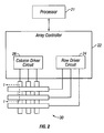
- Figure 2 is a system block diagram illustrating one embodiment of an electronic device that may incorporate aspects of the invention.
- the electronic device includes a processor 21 which may be any general purpose single- or multi-chip microprocessor such as an ARM, Pentium®, Pentium II®, Pentium III®, Pentium IV®, Pentium® Pro, an 8051, a MIPS®, a Power PC®, an ALPHA®, or any special purpose microprocessor such as a digital signal processor, microcontroller, or a programmable gate array.
- the processor 21 may be configured to execute one or more software modules.
- the processor may be configured to execute one or more software applications, including a web browser, a telephone application, an email program, or any other software application.
- the processor 21 is also configured to communicate with an array controller 22.
- the array controller 22 includes a row driver circuit 24 and a column driver circuit 26 that provide signals to a pixel array 30.
- the cross section of the array illustrated in Figure 1 is shown by the lines 1-1 in Figure 2.
- the row/column actuation protocol may take advantage of a hysteresis property of these devices illustrated in Figure 3. It may require, for example, a 10 volt potential difference to cause a movable layer to deform from the released state to the actuated state. However, when the voltage is reduced from that value, the movable layer maintains its state as the voltage drops back below 10 volts.
- the movable layer does not release completely until the voltage drops below 2 volts.
- the row/column actuation protocol can be designed such that during row strobing, pixels in the strobed row that are to be actuated are exposed to a voltage difference of about 10 volts, and pixels that are to be released are exposed to a voltage difference of close to zero volts.
- each pixel sees a potential difference within the "stability window" of 3-7 volts in this example.
- This feature makes the pixel design illustrated in Figure 1 stable under the same applied voltage conditions in either an actuated or released pre-existing state. Since each pixel of the interferometric modulator, whether in the actuated or released state, is essentially a capacitor formed by the fixed and moving reflective layers, this stable state can be held at a voltage within the hysteresis window with almost no power dissipation. Essentially no current flows into the pixel if the applied potential is fixed.
- a display frame may be created by asserting the set of column electrodes in accordance with the desired set of actuated pixels in the first row.
- a row pulse is then applied to the row 1 electrode, actuating the pixels corresponding to the asserted column lines.
- the asserted set of column electrodes is then changed to correspond to the desired set of actuated pixels in the second row.
- a pulse is then applied to the row 2 electrode, actuating the appropriate pixels in row 2 in accordance with the asserted column electrodes.
- the row 1 pixels are unaffected by the row 2 pulse, and remain in the state they were set to during the row 1 pulse. This may be repeated for the entire series of rows in a sequential fashion to produce the frame.
- the frames are refreshed and/or updated with new display data by continually repeating this process at some desired number of frames per second.
- protocols for driving row and column electrodes of pixel arrays to produce display frames are also well known and may be used in conjunction with the present invention.
- Figures 4, 5A, and 5B illustrate one possible actuation protocol for creating a display frame on the 3x3 array of Figure 2.
- Figure 4 illustrates a possible set of column and row voltage levels that may be used for pixels exhibiting the hysteresis curves of Figure 3.
- actuating a pixel involves setting the appropriate column to -V bias, and the appropriate row to + ⁇ V, which may correspond to -5 volts and +5 volts respectively Releasing the pixel is accomplished by setting the appropriate column to +V bias, and the appropriate row to the same + ⁇ V, producing a zero volt potential difference across the pixel. In those rows where the row voltage is held at zero volts, the pixels are stable in whatever state they were originally in, regardless of whether the column is at +V bias , or -V bias .
- Figure 5B is a timing diagram showing a series of row and column signals applied to the 3x3 array of Figure 2 which will result in the display arrangement illustrated in Figure 5A, where actuated pixels are non-reflective.
- the pixels Prior to writing the frame illustrated in Figure 5A, the pixels can be in any state, and in this example, all the rows are at 0 volts, and all the columns are at +5 volts. With these applied voltages, all pixels are stable in their existing actuated or released states.
- pixels (1,1), (1,2), (2,2), (3,2) and (3,3) are actuated.
- columns 1 and 2 are set to -5 volts, and column 3 is set to +5 volts. This does not change the state of any pixels, because all the pixels remain in the 3-7 volt stability window.
- Row 1 is then strobed with a pulse that goes from 0, up to 5 volts, and back to zero. This actuates the (1,1) and (1,2) pixels and releases the (1,3) pixel. No other pixels in the array are affected.
- column 2 is set to -5 volts
- columns 1 and 3 are set to +5 volts.
- Row 3 is similarly set by setting columns 2 and 3 to -5 volts, and column 1 to +5 volts.
- the row 3 strobe sets the row 3 pixels as shown in Figure 5A. After writing the frame, the row potentials are zero, and the column potentials can remain at either +5 or -5 volts, and the display is then stable in the arrangement of Figure 5A. It will be appreciated that the same procedure can be employed for arrays of dozens or hundreds of rows and columns. It will also be appreciated that the timing, sequence, and levels of voltages used to perform row and column actuation can be varied widely within the general principles outlined above, and the above example is exemplary only, and any actuation voltage method can be used with the present invention.
- Figures 6A-6C illustrate three different embodiments of the moving mirror structure.
- Figure 6A is a cross section of the embodiment of Figure 1, where a strip of metal material 14 is deposited on orthogonally extending supports 18.
- the moveable reflective material 14 is attached to supports at the comers only, on tethers 32.
- the moveable reflective material 14 is suspended from a deformable layer 34.
- This embodiment has benefits because the structural design and materials used for the reflective material 14 can be optimized with respect to the optical properties, and the structural design and materials used for the deformable layer 34 can be optimized with respect to desired mechanical properties.
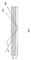
- Figure 7 is a side cross-sectional view of an interferometric modulator 12 illustrating optical paths through the modulator 12.
- the color of light reflected from the interferometric modulator 12 may vary for different angles of incidence (and reflection) as illustrated in Figure 7.
- the interferometric modulator 12 shown in Figure 7 as light travels along path A 1 , the light is incident on the interferometric modulator at a first angle, reflects from the interferometric modulator, and travels to a viewer. The viewer perceives a first color when the light reaches the viewer as a result of optical interference between a pair of mirrors in the interferometric modulator 12.
- Optical interference in the interferometric modulator 12 depends on optical path length of light propagated within the modulator. Different optical path lengths for the different optical paths A 1 and A 2 therefore yield different outputs from the interferometric modulator 12. The user therefore perceives different colors depending on his or her angle of view. This phenomenon is referred to as a "color shift".
- the amount of color shift may be expressed in terms of a difference in wavelength, e.g., in nanometers, for the light emitted from the interferometric modulators for different angles of incident (and reflected light). As is well known, for spectral reflection, the angle of incidence is equal to the angle of reflection.
- the wavelength used to measure the color shift may be the peak wavelength of the specular distribution of light output from the interferometric modulator.
- specular distribution refers to the wavelength distribution, such as for example, the intensity of light at different wavelengths.
- the output of the interferometric modulator 12 may be characterized by a spectral responsivity function or spectral response R ( ⁇ i, ⁇ ), where ⁇ i is the angle of incidence of light and ⁇ is the wavelength.
- ⁇ i is the angle of incidence of light
- ⁇ is the wavelength.
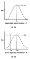
- Figure 8 schematically illustrates exemplary spectral responses R ( ⁇ i , ⁇ ) for different angles of incidence.
- a first plot 110 for example, shows a spectral response (output versus wavelength) for a first angle of incidence.
- a second plot 120 shows a spectral response for a second angle of incidence.
- the first and second plots each have peaks 115, 125, sometime referred to herein as spectral lines. These plots 110, 120 and the corresponding peaks are shifted from each other. The shift in the peaks 115, 125 for the different plots shows the color shift with angle of view.
- a certain amount of perceived off-axis color shift in a display may be tolerated for certain displays.
- a color shift or a change e.g., of about 5-30 nanometers in wavelength for an angle of view shift of about 40° may be acceptable for certain applications.
- the color shift is too significant and is noticeable by the observer.
- methods of correcting or compensating for such intolerable color shifts as described herein may be employed.
- the level of tolerance that is permissible may depend upon factors that include the intended use of the display, the quality, and/or the price range of the display.
- the level of "tolerance” in color shift may be expressed in terms of nanometers of wavelength shift for a change in view angle of a specified range.
- the tolerance may be expressed for a range between about -60° and 60°.
- the tolerance may be expressed for a range between about -80° and 80°
- a diffuser may be used to compensate for the color shift of an interferometric modulator structure.
- Figure 9 shows one embodiment of interferometric modulator display 200 that includes a diffuser layer 201.
- the interferometric modulator display 200 includes a transparent substrate 20, such as glass, having a viewing surface to which the diffuser layer 201 is attached.
- the diffuser layer 201 is formed on the top side of the substrate 20 as shown in Figure 9. Other designs are also possible.
- Diffusers may comprise bulk diffuser material.
- a diffuser may include one or more layers of a material such as a suitable transparent or translucent polymer resin, for example, polyester, polycarbonate, polyvinyl chloride (PVC), polyvinylidene chloride, polystyrene, polyacrylates, polyethylene terephthalate, polyurethane, and copolymers or blends thereof. Other materials may be employed as well.
- the diffuser is attached to a surface of the substrate using a double-sided adhesive.
- Figure 10 is a graphical diagram 300 of exemplary optical responses, referred to as D( ⁇ i , ⁇ ), for a diffuser or diffuser material in accordance embodiments of the invention.
- Output from the diffuser may depend on both angle of incidence ⁇ i and on angle of transmission or angle of view, ⁇ .
- the optical transfer function D( ⁇ i , ⁇ ) may be expressed as a function of the angle of view "0" and the angle of incidence of light " ⁇ i " ranging, e.g., from 0 to 90° or from 0 to - 90°.
- the vertical axis depicts the relative intensity of light from a light source that is observed through a diffuser.
- the horizontal axis represents the angle of viewing of light communicated through the diffuser.
- the possible angle of view varies from 0 to 90 degrees on the right side of graph and from 0 to -90 degrees ⁇ left side of graph 300).
- Curves or traces 310, 320, and 330 in Figure 10 depict the optical response of diffusers for a given angle of incidence, ⁇ i as the output varies with transmission angle or view angle ⁇ .
- This angle of incidence may, for example, be 0° for the plots 310, 320, 330 in Figure 10.
- the first trace 310 depicts the perceived intensity of light versus angle of viewing for a particular diffuser (and a particular angle of incidence).
- the trace 310 has a generally a bell-shaped curve that has a relatively sharp peak at a center angle.
- the sharp or relatively narrow peak is located at 0° for this embodiment of the diffuser.
- This narrow peak may for example have a width as measured at full width half maximum of about 10-30°.
- This type of trace is sometimes referred to as a high gain curve.
- the trace 320 depicts an optical response for a second type of diffuser.
- the trace 320 is a generally bell-shaped curve that has a relatively small wider peak at its center. This narrow peak may for example have a width as measured at full width half maximum of about 60-100°
- the trace 320 with its relatively low peak and thus somewhat flattened response profile is sometimes referred to as a low gain curve.
- each optical response is shown as centered at about 0° for the purpose of illustration. As will be discussed further below, the optical response may be centered at other angles for different diffusers.
- Figure 10 shows a trace 330 depicting the optical response of an ideal Lambertian diffuser.
- Lambertian diffusers are characterized by a substantially flat angular response profile.
- the trace 330 depicts an approximately straight line response having a generally fixed intensity at all angles of viewing.
- non-lambertian diffusers do not have substantially flat angular response profiles.
- the high gain and low gain diffusers corresponding to traces 310 and 320 are examples of non-lambertian diffusers.
- the traces 310 and 320 illustrate optical responses of various diffusers having responses that are centered around zero degrees (0°).
- similar shaped (or other shaped) response profiles may be centered on view angles other than zero degrees, such as, for example, at ten (10), twenty (20), thirty (30), forty (40), 45 (forty five), 50 (fifty), 60 (sixty), 70 (seventy), 80 (eighty) degrees, or on any other view angle.
- D( ⁇ i , ⁇ ) may be characterized by a response profile that may be different characteristically for different angles of view.
- the diffuser 201 may be a high gain, low gain (or very low gain), or any other suitable type of diffuser therebetween, or any combination thereof.
- the centering of D( ⁇ i , ⁇ ) around a particular angle is relevant to computing a convolution of D( ⁇ i , ⁇ ) and optical response of the interferometric modulator, without the diffuser, which is referred to as R ( ⁇ i , ⁇ )
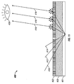
- Figure 11 is a cross-sectional view illustrating an embodiment of an interferometric modulator display 400 that includes a diffuser 402.
- the display 400 includes an array of interferometric modulators 401.
- the diffuser 402 is physically coupled to a substrate 403. Light is reflected in the interferometric modulator 401 so as to pass outward through the diffuser 402.
- the diffuser 402 is selected based on its characteristics which influence the reflected light so as to compensate for at least a portion of the angular color shift of the interferometric modulator 401. This compensation reduces the perceived color shift as the viewing angle of a user of the modulator 401 changes.
- any numerical values used herein, such as the angles of incidence of light paths 410, 412, and 414, are presented for purposes of illustration and are not necessarily indicative of any embodiment.
- the modulator 401 reflects the light further along the paths 410, 412, and 414.
- the light along the paths 410, 412, and 414 is then incident on the diffuser 402.
- the diffuser 402 redirects portions of the reflected light along a range of optical paths at intensities that depend upon the gain characteristics, D( ⁇ i , ⁇ ), of the diffuser 402.
- the diffused portion of the light from optical paths 410, 412, and 414 travels to a viewing position along optical paths 416.
- These paths 416 are at substantially the same angle with respect to the diffuser 402 and substantially parallel for this particular exemplary viewing position 430 which is a distant viewing position.
- the diffuser 402 thus operates to collect light that is incident on the modulator 401 at a range of angles and corresponding optical paths, including the paths 410, 412, and 414. This collected light is redirected. A portion of this light is redirected to the viewing position along the optical paths 416.
- the diffuser 402 thus collects light from the modulator 401 (or array of modulators 401) at a range of wavelengths to produce a net optical response for the modulator 401 as modified by the diffuser 402.
- the net optical response is related to the convolution of the optical response D( ⁇ i , ⁇ ) of the diffuser with the optical response R ( ⁇ i , ⁇ ) of the modulator 401 over a range of angles of light incident on the display 400.
- the net optical response of the system 400 can thus be controlled to achieve a desired net optical response.
- the characteristics of the diffuser 402 and the interferometric modulator 401 are selected so as to substantially compensate for angular color shift of the interferometric modulator 401.
- the characteristics of the diffuser 402 and the modulator 401 are selected so that an image formed by the modulator array alone is obscured or encrypted and is not visible. The image formed by the modulator array, however, is visible by viewing through the diffuser 402.
- the overall optical characteristics of the modulator 401 together with the diffuser 402 may be modeled in terms of the convolution of the optical response (i.e., spectral reflectance or transfer function) of the modulator 401, with the optical response of the diffuser 402.
- An exemplary expression for this convolution is set forth below.
- the optical response R ( ⁇ i , ⁇ ) of the modulator 401 is represented as a function of the angle of incidence, ⁇ i , and wavelength of light, ⁇ , entering the modulator 401.
- the angle of incidence is equal to the angle of reflection for specular reflection
- the view angle, 0, for the modulator is equal to the angle of incidence, ⁇ i , on the modulator.
- R ( ⁇ i , ⁇ ) characterizes the optical response of the modulator as a function of view angle, 0.
- the intensity of the light coming out of the diffuser 402 is also generally a function of the viewing angle ⁇ (and angle of incidence ⁇ i ). Accordingly, as described above, the optical response of the diffuser is characterized by D( ⁇ i , ⁇ ).
- the view angle, ⁇ , of the modulator corresponds to the angle of incidence, ⁇ i , of the diffuser.
- the modified spectral reflectance R' ( ⁇ , ⁇ ) that includes the effects of the diffuser 402 can be computed.
- the result is spectral response of the display for a given view angle ⁇ .
- the spectral response of the combination of the modulator 401 and the diffuser 402 can thus be computed for a particular viewing angle and corresponding viewer position.
- the spectral response for the aggregate structure comprising the modulator 401 and the diffuser 402 may be computed for multiple viewing angles and view positions to quantify color shift resulting from change in angle of view.
- R' ( ⁇ , ⁇ ) it is desirable to define the type of overall or corrected reflectance (i.e., R' ( ⁇ , ⁇ )) in terms of particular criteria, e.g., acceptable or unacceptable level of color shift. For example, if the color shift at a particular angle of view (e.g., 30 degrees) is 100 nanometers, it may be desirable to reduce such color shift to no more than 20 nanometers. In such a case, the uncompensated optical response R ( ⁇ i , ⁇ ) of the modulator 401 having an undesirable 100-nanometer color shift (e.g., at 30 degrees) may be improved with a suitable diffuser so as to provide a resultant spectral response R' ( ⁇ , ⁇ )) having an acceptable 20-nanometer color shift. It is worth noting that these numbers are chosen arbitrarily for illustrative purpose, and any tolerance level in color shift may be used in practice. For instance in certain embodiments, the level of tolerance in color shift characteristics may depend on intended use or planned viewing conditions.
- the desirable optical response R'( ⁇ , ⁇ ) is derivable from the uncompensated optical response R ( ⁇ i , ⁇ ).
- the optical response of uncompensated R ( ⁇ i , ⁇ ) and desired R '( ⁇ , ⁇ ) are known functions
- the optical response (i.e., characteristics) for D( ⁇ i , ⁇ ) can be computed from the above equation. Since the above equation has only one unknown variable, D( ⁇ i , ⁇ ) can be determined to define the suitable diffuser for providing the desired spectral responsivity R'( ⁇ , ⁇ ).
- the D( ⁇ i, ⁇ ), once solved may, for example, correspond to a diffuser having a high gain, a low gain, or a very low gain response, or other suitable characteristics.
- D( ⁇ i , ⁇ ) is determined by solving permutations of the equation above (e.g., solving the deconvolution).
- Well known mathematical and numerical methods may be employed to perform the calculations.
- diffusers may be fabricated to provide a desired optical response. Accordingly, once characteristics of D ( ⁇ i , ⁇ ) are determined, a suitable physical configuration and material of the diffuser 402 may then be determined to produce at least an approximation of the desired response profile D ( ⁇ i , ⁇ ) such that the color shift is within a desired tolerance at the target angle.
- the physical configuration may be determined using techniques such as are known in the art. Diffusers with selected properties are available, for example, from Nitto Denko, Osaka, Japan. Additional details regarding selecting a diffuser based on the spectral response of the interferometric modulator are discussed more fully below.
- the diffuser 402 is a diffuser having high gain characteristics that may be selected to reduce or compensate for the color shift.
- Figure 12A is a graphical diagram illustrating the gain of the exemplary diffuser 402 versus angle of view for an angle of incidence of 0°.
- Figure 12B is a graphical diagram illustrating the gain of the exemplary diffuser 402 versus angle of view at an angle of incidence of 10°.
- R ( ⁇ i , ⁇ ) [ 0.5 0.9 ]
- R ( 10 ° , ⁇ ) [ 0.6 0.8 ]
- the calculations are illustrated using only two angles of incidence for a single wavelength, are provided.
- the convolution is calculated for angle of incidence ranging from 0 to 10° with a step size of 10°.
- a larger range of angles may be used and the step size may be different.
- values for various wavelengths may be identified at any particular angle of incidence (or angle of view); in this example, only 0° and 10° are being used.
- wavelengths at each angle of view there are many different wavelengths at each angle of view; however only two values (0.5 and 0.9) for the wavelength, ⁇ , are provided at 0 degrees (angle of incidence ⁇ i or angle of view) for illustration only. Similarly, two values (0.6 and 0.8) for the wavelength, ⁇ , are provided at an angle of view of 10 degrees.
- R '( ⁇ , ⁇ ) the actual optical response D( ⁇ i , ⁇ ) of the diffuser 402.
- the equation above is used to compute R '( ⁇ , ⁇ ) at a desired angle of view.
- R' ( ⁇ , ⁇ ) can be computed at an angle of view of 10° (or at any desired angle of view, e.g., between 0° and 90°, in a like manner).
- the convolution is summed by varying ⁇ i from 0° to 90° to compute the total modified or compensated optical response R '( ⁇ , ⁇ ) (as corrected by the diffuser 402).
- the diffuser 402 may include more than one diffuser layer. In one such embodiment, the same diffuser characteristics may be selected for each of the diffuser layers. In another embodiment, different characteristics may be selected for each of the layers of the diffuser 402. In one embodiment, the diffuser characteristics of the diffuser 402 may be calculated by convolving the optical responses of each of the layers.
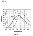
- Figure 13 illustrates a graphical diagram 500 of several spectral reflectance traces for various configurations of interferometric modulator display devices.
- the vertical axis represents a reflectance to the viewer, expressed as a percentage (from 0 to 90%).
- the horizontal axis represents the wavelength of light that is reflected by the interferometric modulator. This reflectance corresponds to the spectral responsivity e.g., R(Q, ⁇ ), R'( ⁇ , ⁇ ), described above.
- curve 510 depicts a somewhat bell-shaped curve that represents the reflectance as viewed at 0 degrees to normal from the display of one or more interferometric modulators (without the presence of a diffuser layer).
- the peak of curve 510 is at approximately 80% reflectance and is centered about 820 nm, which is in the infrared portion of the spectrum.
- Figure 13 further depicts a curve 520 that represents the reflectance of this same display as viewed at 50 degrees to normal.
- the curve 520 is shaped similarly to the curve 510 but has a peak value of reflectance of approximately 84% that is located at about 690 nm.
- Figure 13 also depicts a somewhat bell-shaped curve 530 that represents the reflectance as viewed at 0 degrees to normal from a display that includes a diffuser layer.
- the curve 530 has a peak gain of approximately 64% that is located approximately at 750 nm.
- Figure 13 depicts a curve 540 that represents the reflectance of the display having the diffuser layer as viewed at 50 degrees to normal.
- the curve 540 follows a path that is substantially the same as the path of curve 530 with a slightly smaller peak reflectance value of 62%.
- Figure 13 shows the reflectance from the modulator using input light to the interferometric modulator that is in the infrared portion of the electromagnetic spectrum at about a peak wavelength of 810 nanometers (nm).
- the 50 degree shift in viewing angle causes an approximately 120 nm color shift in the viewed response profile.
- the curves 530 and 540 illustrate the spectral reflectance of the modulator when viewed through a very low gain diffuser 302 having a full width half maximum gain between 120° and 180°.
- the curves 530 and 540 represent the convolution of the response of this very low gain diffuser with that of the interferometric modulator.
- both curves 530 and 540 peak at about the same or a similar wavelength that is horizontally between the peaks of curves 510 and 520.
- the curves thus exhibit a very minor perceived color shift (such as in the range of about 10 to 20 nm) when the viewing angle changes by fifty degrees (50°), as in this example.
- the diffuser layer As compared to the 120 nm color shift of the modulator viewed at 50° without the diffuser layer, the diffuser layer has thus been substantially compensated for the shift in viewing angle.
- the peaks of the curves 530 and 540 do not shift in color substantially with changing viewing angle.
- the peaks of curves for the modulator without the diffuser that were in the infrared portion of the spectrum are in the red portion of the spectrum with the low gain diffuser.
- the diffuser has therefore shifted the spectral responsivity of an interferometric modulator have a peak response in the infrared to a device having a peak in a visible wavelength.
- Another characteristic of the effect of the diffuser is that the peak spectral reflectance of the convoluted, e.g., perceived, light signal is reduced and spread more evenly across the spectrum.
- the color shift and the amount of the drop in peak reflectance may be controlled by selecting the desired wavelength and angle for the peak of the curve for a diffuser.
- the selected diffuser may have a response that is centered about 0°.
- the selected diffuser may have a response centered around an angle other than 0°, for example, centered at ten (10°), twenty (20), thirty (30), forty (40), 45 (forty five), 50 (fifty), 60 (sixty), 70 (seventy), 80 (eighty) degrees, or on any other view angle.
- Figure 14 is a CIE 1976 chromaticity diagram 600 that illustrates a sequence of data points that show color shift versus view angle to further illustrate the effect of the embodiment of the diffuser 401 from Figure 13.
- the horizontal and vertical axes define a chromaticity coordinate system on which spectral tri-stimulus values may be depicted.
- a sequence of data points for an interferometric modulator display without diffuser is shown on the gamut color space of the diagram along a trace 605.
- the curve of the trace 605 indicates that there is a considerable color shift for changes in the view angle.
- a single data point 610 is shown on the diagram 401 because the color shift has been substantially eliminated by use of the diffuser layer
- a diffuser can be selected having specific properties that produce a desired spectral responsivity, R '( ⁇ , ⁇ ). Examples of properties that can be varied include the shape of the optical response D( ⁇ i , ⁇ ).
- the diffuser may comprise, e.g., a non-lambertian diffuser such as a high gain, low gain, or very low gain diffuser.
- the optical response D( ⁇ i , ⁇ ) comprises a peak
- the width of this peak can be selected. For example, peaks as measured at full width half maximum may be between about 2° to 20° wide in some embodiments or between about 20 to 120 wide or larger or smaller. Peaks widths outside these ranges are also possible.
- the position of this peak can be controlled.
- the high and low gain response shown in Figure 10 are centered about 0°, in certain embodiments, diffusers having peaked optical response with peak at locations other than 0° may be used. Other properties of the diffuser may be varied as well.
- the optical responses depicted in Figure 10 are for a particular angle of incidence; however, D( ⁇ i , ⁇ ) is also a function of ⁇ i .
- the diffuser may be configured to provide different optical responses D( ⁇ ) for light incident at different angles of incidence ⁇ i .
- the diffuser may be designed such that the width and location of peaks in the optical response are different for differing angles of incidence.
- the peak may for example be located at an angle of view equal (but opposite) to the angle of incidence.
- the angle of view of the peak may be different in magnitude from the angle of incidence.
- the spectral responsivity of the interferometric modulator varies with angle, different responses for different angles of incidence may be employed to redistribute the rays to achieve the desired dependency of color on view angle. Accordingly, reduced color shift may be achieved by properly distributing the light incident on the diffuser at different angles.
- the desired spectral responsivity R' ( ⁇ , ⁇ ) may be obtained.
- Consideration of the spectral responsivity R( ⁇ i , ⁇ ) of the interferometric modulator may be used in determining the properties of such a suitable diffuser. Accordingly, a diffuser may be selected that appropriately matches the interferometric modulator so as, for example, to reduce color shift.
- the selection and/or design of the diffuser may be based on the known spectral and angular optical response of diffuser materials and architectures.
- the diffuser is selected or designed so that the convolution of the diffuser's optical response with that of the interferometric modulator 401 produces an optical response that decreases the color shift.
- the color shift as viewed from at least one target angle may be reduced to within a predetermined tolerance for a particular viewing angle and particular interferometric modulator configuration 401.
- the predetermined tolerance may be expressed as a number of nanometers of color shift.
- Holographic or diffractive optical elements may be employed as the diffuser.
- the diffusers may also be computer generated.
- the desired optical response for the diffuser is produced by selecting materials, thicknesses, and arrangement of the materials of the diffuser to produce the desired optical response for the diffuser.
- the interferometric modulator has a spectral response (e.g., for viewing angles at normal incidence) that is centered in the infrared or other non-visible wavelength.
- a spectral response having mostly non-visible components may contribute to reduced color shifting. For example 50%, 60%, 70% or more of the wavelengths under a central peak that extends in the visible may be non-visible. The diffuser may shift this peak into the visible.
- the diffuser may exhibit a response D( ⁇ i , ⁇ , ⁇ ) that is a function of wavelength.
- the diffuser includes a holographic optical element. Other types of wavelength sensitive diffusers may be employed as well.
- a back light or front light may be added to provide additional intensity at desired wavelengths.
- the use of such frequency dependent diffuser configurations and light sources provides additional flexibility in selecting a configuration that may be viewed at a selected angle with a predetermined tolerance on color shift.
- the display 400 may include interferometric modulators 401 that have varying optical responses.
- the display 400 includes three groups of interferometric modulators 401 having optical responses that, when the modulators 401 are matched with the diffuser 402 as disclosed herein, correspond to red, green, and blue to produce a color display.
- the optical response of diffuser 402 may depend on the wavelength ⁇ of light passing through the diffuser 402.
- the diffuser 402 comprises a holographic optical element.
- a combination of several diffusers may be used to provide a display with angular color shift at a selected angle that is within a predetermined tolerance.
- one or more diffusers may be used to provide a color shift that is within a predetermined tolerance for two, three, or a range of angles. Still other configurations are possible.
- an application of the interferometric modulator with diffuser is to enable encryption or obscuring of the image of a display to secure the image from unauthorized viewing.
- the diffuser moves data from an invisible portion of the spectrum, e.g., infrared, to a visible portion of the spectrum.
- the diffuser may be positioned with respect to the interferometric modulator array so that authorized viewers receive light from the display through the diffuser.
- the interferometric modulator produces an encrypted image and the diffuser is configured to decrypt the image.
- the interferometric modulator array of the display has an optical response that is selected to receive input image data and produce an output image that is difficult for the human eye to perceive, for example, in which colors are shifted such that the image is obscured.
- the diffuser is selected to shift the colors to a produce an image with colors indicative of the input image data.
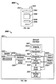
- FIGS 15A and 15B are system block diagrams illustrating an embodiment of a display device 2040.
- the display device 2040 can be, for example, a cellular or mobile telephone.
- the same components of display device 2040 or slight variations thereof are also illustrative of various types of display devices such as televisions and portable media players.
- the display device 2040 includes a housing 2041, a display 2030, an antenna 2043, a speaker 2045, an input device 2048, and a microphone 2046.
- the housing 2041 is generally formed from any of a variety of manufacturing processes as are well known to those of skill in the art, including injection molding, and vacuum forming.
- the housing 2041 may be made from any of a variety of materials, including but not limited to plastic, metal, glass, rubber, and ceramic, or a combination thereof.
- the housing 2041 includes removable portions (not shown) that may be interchanged with other removable portions of different color, or containing different logos, pictures, or symbols.
- the display 2030 of exemplary display device 2040 may be any of a variety of displays, including a bi-stable display, as described herein.
- the display 2030 includes a flat-panel display, such as plasma, EL, OLED, STN LCD, or TFT LCD as described above, or a non-flat-panel display, such as a CRT or other tube device, as is well known to those of skill in the art.
- the display 2030 includes an interferometric modulator display, as described herein.
- the components of one embodiment of exemplary display device 2040 are schematically illustrated in Figure 15B.
- the illustrated exemplary display device 2040 includes a housing 2041 and can include additional components at least partially enclosed therein.
- the exemplary display device 2040 includes a network interface 2027 that includes an antenna 2043 which is coupled to a transceiver 2047.
- the transceiver 2047 is connected to the processor 2021, which is connected to conditioning hardware 2052.
- the conditioning hardware 2052 may be configured to condition a signal (e.g. filter a signal).
- the conditioning hardware 2052 is connected to a speaker 2045 and a microphone 2046.
- the processor 2021 is also connected to an input device 2048 and a driver controller 2029.
- the driver controller 2029 is coupled to a frame buffer 2028 and to the array driver 2022, which in turn is coupled to a display array 2030.
- a power supply 2050 provides power to all components as required by the particular exemplary display device 2040 design.
- the network interface 2027 includes the antenna 2043 and the transceiver 2047 so that the exemplary display device 2040 can communicate with one or more devices over a network. In one embodiment the network interface 2027 may also have some processing capabilities to relieve requirements of the processor 2021.
- the antenna 2043 is any antenna known to those of skill in the art for transmitting and receiving signals. In one embodiment, the antenna transmits and receives RF signals according to the IEEE 802.11 standard, including IEEE 802.11(a), (b), or (g). In another embodiment, the antenna transmits and receives RF signals according to the BLUETOOTH standard. In the case of a cellular telephone, the antenna is designed to receive CDMA, GSM, AMPS or other known signals that are used to communicate within a wireless cell phone network.
- the transceiver 2047 pre-processes the signals received from the antenna 2043 so that they may be received by and further manipulated by the processor 2021.
- the transceiver 2047 also processes signals received from the processor 2021 so that they may be transmitted from the exemplary display device 2040 via the antenna 2043.
- the transceiver 2047 can be replaced by a receiver.
- network interface 2027 can be replaced by an image source, which can store or generate image data to be sent to the processor 2021.
- the image source can be a digital video disc (DVD) or a hard-disc drive that contains image data, or a software module that generates image data.
- Processor 2021 generally controls the overall operation of the exemplary display device 2040.
- the processor 2021 receives data, such as compressed image data from the network interface 2027 or an image source, and processes the data into raw image data or into a format that is readily processed into raw image data.
- the processor 2021 then sends the processed data to the driver controller 2029 or to frame buffer 2028 for storage.
- Raw data typically refers to the information that identifies the image characteristics at each location within an image. For example, such image characteristics can include color, saturation, and gray-scale level.
- the processor 2021 includes a microcontroller, CPU, or logic unit to control operation of the exemplary display device 2040.
- Conditioning hardware 2052 generally includes amplifiers and filters for transmitting signals to the speaker 2045, and for receiving signals from the microphone 2046.
- Conditioning hardware 2052 may be discrete components within the exemplary display device 2040, or may be incorporated within the processor 2021 or other components.
- the driver controller 2029 takes the raw image data generated by the processor 2021 either directly from the processor 2021 or from the frame buffer 2028 and reformats the raw image data appropriately for high speed transmission to the array driver 2022. Specifically, the driver controller 2029 reformats the raw image data into a data flow having a raster-like format, such that it has a time order suitable for scanning across the display array 2030. Then the driver controller 2029 sends the formatted information to the array driver 2022.
- a driver controller 2029 such as a LCD controller, is often associated with the system processor 2021 as a stand-alone Integrated Circuit (IC), such controllers may be implemented in many ways. They may be embedded in the processor 2021 as hardware, embedded in the processor 2021 as software, or fully integrated in hardware with the array driver 2022.
- IC Integrated Circuit
- the array driver 2022 receives the formatted information from the driver controller 2029 and reformats the video data into a parallel set of waveforms that are applied many times per second to the hundreds and sometimes thousands of leads coming from the display's x-y matrix of pixels.
- driver controller 2029, array driver 2022, and display array 2030 are appropriate for any of the types of displays described herein.
- driver controller 2029 is a conventional display controller or a bi-stable display controller (e.g., an interferometric modulator controller).
- array driver 2022 is a conventional driver or a bi-stable display driver (e.g., an interferometric modulator display).
- a driver controller 2029 is integrated with the array driver 2022.
- display array 2030 is a typical display array or a bi-stable display array (e.g., a display including an array of interferometric modulators).
- the input device 2048 allows a user to control the operation of the exemplary display device 2040.
- input device 2048 includes a keypad, such as a QWERTY keyboard or a telephone keypad, a button, a switch, a touch-sensitive screen, a pressure- or heat-sensitive membrane.
- the microphone 2046 is an input device for the exemplary display device 2040. When the microphone 2046 is used to input data to the device, voice commands may be provided by a user for controlling operations of the exemplary display device 2040.
- Power supply 2050 can include a variety of energy storage devices as are well known in the art.
- power supply 2050 is a rechargeable battery, such as a nickel-cadmium battery or a lithium ion battery.
- power supply 2050 is a renewable energy source, a capacitor, or a solar cell, including a plastic solar cell, and solar-cell paint.
- power supply 2050 is configured to receive power from a wall outlet.
- control programmability resides, as described above, in a driver controller which can be located in several places in the electronic display system. In some cases control programmability resides in the array driver 2022. Those of skill in the art will recognize that the above-described optimization may be implemented in any number of hardware and/or software components and in various configurations.
Priority Applications (1)
| Application Number | Priority Date | Filing Date | Title |
|---|---|---|---|
| EP11157386A EP2388234A1 (fr) | 2004-09-27 | 2005-09-14 | Procédé et dispositif pour compenser un décalage de couleur en fonction de l'angle de vue |
Applications Claiming Priority (2)
| Application Number | Priority Date | Filing Date | Title |
|---|---|---|---|
| US61397804P | 2004-09-27 | 2004-09-27 | |
| US11/040,824 US7630123B2 (en) | 2004-09-27 | 2005-01-21 | Method and device for compensating for color shift as a function of angle of view |
Publications (2)
| Publication Number | Publication Date |
|---|---|
| EP1640314A2 true EP1640314A2 (fr) | 2006-03-29 |
| EP1640314A3 EP1640314A3 (fr) | 2008-04-09 |
Family
ID=35462167
Family Applications (2)
| Application Number | Title | Priority Date | Filing Date |
|---|---|---|---|
| EP05255647A Withdrawn EP1640314A3 (fr) | 2004-09-27 | 2005-09-14 | Méthode et dispositif pour compensation du décalage de couleurs en fonction de l'angle de vue |
| EP11157386A Withdrawn EP2388234A1 (fr) | 2004-09-27 | 2005-09-14 | Procédé et dispositif pour compenser un décalage de couleur en fonction de l'angle de vue |
Family Applications After (1)
| Application Number | Title | Priority Date | Filing Date |
|---|---|---|---|
| EP11157386A Withdrawn EP2388234A1 (fr) | 2004-09-27 | 2005-09-14 | Procédé et dispositif pour compenser un décalage de couleur en fonction de l'angle de vue |
Country Status (11)
| Country | Link |
|---|---|
| US (3) | US7630123B2 (fr) |
| EP (2) | EP1640314A3 (fr) |
| JP (1) | JP2006099102A (fr) |
| KR (1) | KR101236289B1 (fr) |
| AU (1) | AU2005204303A1 (fr) |
| BR (1) | BRPI0503907A (fr) |
| CA (1) | CA2519485A1 (fr) |
| MX (1) | MXPA05010094A (fr) |
| RU (1) | RU2005129902A (fr) |
| SG (1) | SG121151A1 (fr) |
| TW (1) | TW200624368A (fr) |
Cited By (9)
| Publication number | Priority date | Publication date | Assignee | Title |
|---|---|---|---|---|
| WO2008144221A1 (fr) * | 2007-05-18 | 2008-11-27 | Qualcomm Mems Technologies, Inc. | Afficheur de modulateur interférométrique ayant une sensibilité moins élevée à la variation chromatique |
| US7710636B2 (en) | 2004-09-27 | 2010-05-04 | Qualcomm Mems Technologies, Inc. | Systems and methods using interferometric optical modulators and diffusers |
| US7777954B2 (en) | 2007-01-30 | 2010-08-17 | Qualcomm Mems Technologies, Inc. | Systems and methods of providing a light guiding layer |
| US7813026B2 (en) | 2004-09-27 | 2010-10-12 | Qualcomm Mems Technologies, Inc. | System and method of reducing color shift in a display |
| US7845841B2 (en) | 2006-08-28 | 2010-12-07 | Qualcomm Mems Technologies, Inc. | Angle sweeping holographic illuminator |
| US7907319B2 (en) | 1995-11-06 | 2011-03-15 | Qualcomm Mems Technologies, Inc. | Method and device for modulating light with optical compensation |
| US8111445B2 (en) | 2004-02-03 | 2012-02-07 | Qualcomm Mems Technologies, Inc. | Spatial light modulator with integrated optical compensation structure |
| US9019183B2 (en) | 2006-10-06 | 2015-04-28 | Qualcomm Mems Technologies, Inc. | Optical loss structure integrated in an illumination apparatus |
| US9025235B2 (en) | 2002-12-25 | 2015-05-05 | Qualcomm Mems Technologies, Inc. | Optical interference type of color display having optical diffusion layer between substrate and electrode |
Families Citing this family (28)
| Publication number | Priority date | Publication date | Assignee | Title |
|---|---|---|---|---|
| US8928967B2 (en) | 1998-04-08 | 2015-01-06 | Qualcomm Mems Technologies, Inc. | Method and device for modulating light |
| KR100703140B1 (ko) | 1998-04-08 | 2007-04-05 | 이리다임 디스플레이 코포레이션 | 간섭 변조기 및 그 제조 방법 |
| WO2003007049A1 (fr) | 1999-10-05 | 2003-01-23 | Iridigm Display Corporation | Mems et structures photoniques |
| US7855824B2 (en) | 2004-03-06 | 2010-12-21 | Qualcomm Mems Technologies, Inc. | Method and system for color optimization in a display |
| US7508571B2 (en) | 2004-09-27 | 2009-03-24 | Idc, Llc | Optical films for controlling angular characteristics of displays |
| US8004504B2 (en) | 2004-09-27 | 2011-08-23 | Qualcomm Mems Technologies, Inc. | Reduced capacitance display element |
| US7630123B2 (en) | 2004-09-27 | 2009-12-08 | Qualcomm Mems Technologies, Inc. | Method and device for compensating for color shift as a function of angle of view |
| US7916980B2 (en) | 2006-01-13 | 2011-03-29 | Qualcomm Mems Technologies, Inc. | Interconnect structure for MEMS device |
| US7603001B2 (en) * | 2006-02-17 | 2009-10-13 | Qualcomm Mems Technologies, Inc. | Method and apparatus for providing back-lighting in an interferometric modulator display device |
| EP2069838A2 (fr) | 2006-10-06 | 2009-06-17 | Qualcomm Mems Technologies, Inc. | Dispositif d'éclairage intégrant un coupleur de lumière |
| US8872085B2 (en) | 2006-10-06 | 2014-10-28 | Qualcomm Mems Technologies, Inc. | Display device having front illuminator with turning features |
| EP1946162A2 (fr) | 2006-10-10 | 2008-07-23 | Qualcomm Mems Technologies, Inc | Dispositif d'affichage à optiques diffractives |
| US7864395B2 (en) | 2006-10-27 | 2011-01-04 | Qualcomm Mems Technologies, Inc. | Light guide including optical scattering elements and a method of manufacture |
| US7719752B2 (en) | 2007-05-11 | 2010-05-18 | Qualcomm Mems Technologies, Inc. | MEMS structures, methods of fabricating MEMS components on separate substrates and assembly of same |
| US8986812B2 (en) | 2007-07-09 | 2015-03-24 | 3M Innovative Properties Company | Thin microstructured optical films |
| CN101809471B (zh) | 2007-07-31 | 2013-12-25 | 高通Mems科技公司 | 用于增强干涉式调制器的色彩偏移的装置 |
| US8072402B2 (en) | 2007-08-29 | 2011-12-06 | Qualcomm Mems Technologies, Inc. | Interferometric optical modulator with broadband reflection characteristics |
| US8068710B2 (en) | 2007-12-07 | 2011-11-29 | Qualcomm Mems Technologies, Inc. | Decoupled holographic film and diffuser |
| WO2009102731A2 (fr) | 2008-02-12 | 2009-08-20 | Qualcomm Mems Technologies, Inc. | Dispositifs et procédés permettant d'améliore la luminosité d'écrans utilisant des couches de conversion d'angle |
| WO2009102733A2 (fr) | 2008-02-12 | 2009-08-20 | Qualcomm Mems Technologies, Inc. | Diffuseur de lumiere avant integre pour afficheurs reflechissants |
| WO2009129264A1 (fr) | 2008-04-15 | 2009-10-22 | Qualcomm Mems Technologies, Inc. | Lumière ayant une propagation bidirectionnelle |
| US7864403B2 (en) * | 2009-03-27 | 2011-01-04 | Qualcomm Mems Technologies, Inc. | Post-release adjustment of interferometric modulator reflectivity |
| US8670171B2 (en) | 2010-10-18 | 2014-03-11 | Qualcomm Mems Technologies, Inc. | Display having an embedded microlens array |
| US8902484B2 (en) | 2010-12-15 | 2014-12-02 | Qualcomm Mems Technologies, Inc. | Holographic brightness enhancement film |
| US8717660B2 (en) * | 2012-07-03 | 2014-05-06 | Qualcomm Mems Technologies, Inc. | Annulus scattering diffuser for reflective display |
| CN108281111A (zh) * | 2018-01-19 | 2018-07-13 | 云谷(固安)科技有限公司 | 显示控制方法和装置 |
| US11726365B1 (en) | 2020-07-10 | 2023-08-15 | Meta Platforms Technologies, Llc | Optical assembly for providing koehller illumination to a display |
| US11862083B2 (en) | 2020-08-13 | 2024-01-02 | Apple Inc. | Electronic devices with curved display surfaces |
Citations (4)
| Publication number | Priority date | Publication date | Assignee | Title |
|---|---|---|---|---|
| JPH0922012A (ja) | 1995-07-06 | 1997-01-21 | Mitsubishi Rayon Co Ltd | バックライトおよびそれを用いた液晶表示装置 |
| US20020126364A1 (en) | 1994-05-05 | 2002-09-12 | Iridigm Display Corporation, A Delaware Corporation | Interferometric modulation of radiation |
| JP2003066451A (ja) | 2001-08-30 | 2003-03-05 | Matsushita Electric Ind Co Ltd | 液晶表示装置 |
| US20040125281A1 (en) | 2002-12-25 | 2004-07-01 | Wen-Jian Lin | Optical interference type of color display |
Family Cites Families (383)
| Publication number | Priority date | Publication date | Assignee | Title |
|---|---|---|---|---|
| US2518647A (en) | 1948-01-07 | 1950-08-15 | Celanese Corp | Interferometer means for thickness measurements |
| US3813265A (en) * | 1970-02-16 | 1974-05-28 | A Marks | Electro-optical dipolar material |
| US4863224A (en) | 1981-10-06 | 1989-09-05 | Afian Viktor V | Solar concentrator and manufacturing method therefor |
| JPS5944763U (ja) | 1982-09-13 | 1984-03-24 | 黒崎炉工業株式会社 | ウオ−キングビ−ム式炉 |
| DE3402746A1 (de) | 1984-01-27 | 1985-08-08 | Robert Bosch Gmbh, 7000 Stuttgart | Fluessigkristallanzeige |
| US4832459A (en) * | 1984-02-06 | 1989-05-23 | Rogers Corporation | Backlighting for electro-optical passive displays and transflective layer useful therewith |
| JPS6247841A (ja) | 1985-08-26 | 1987-03-02 | Matsushita Electric Ind Co Ltd | 光学式情報記憶担体 |
| US5835255A (en) | 1986-04-23 | 1998-11-10 | Etalon, Inc. | Visible spectrum modulator arrays |
| US4850682A (en) * | 1986-07-14 | 1989-07-25 | Advanced Environmental Research Group | Diffraction grating structures |
| GB2198867A (en) * | 1986-12-17 | 1988-06-22 | Philips Electronic Associated | A liquid crystal display illumination system |
| EP0278038A1 (fr) | 1987-02-13 | 1988-08-17 | Battelle-Institut e.V. | Ecran de visualisation actif plat |
| US5770626A (en) | 1987-08-19 | 1998-06-23 | Hoffmann-La Roche Inc. | Tetrahydronaphtalene and indane compounds useful for reversing the photodamage in sun-exposed skin |
| JPH01108501U (fr) * | 1988-01-16 | 1989-07-21 | ||
| US4947291A (en) | 1988-06-17 | 1990-08-07 | Mcdermott Kevin | Lighting device |
| US5042921A (en) | 1988-10-25 | 1991-08-27 | Casio Computer Co., Ltd. | Liquid crystal display apparatus |
| US5446479A (en) | 1989-02-27 | 1995-08-29 | Texas Instruments Incorporated | Multi-dimensional array video processor system |
| US4961617A (en) | 1989-07-19 | 1990-10-09 | Ferrydon Shahidi | Fibre optic waveguide illuminating elements |
| JP2893599B2 (ja) * | 1989-10-05 | 1999-05-24 | セイコーエプソン株式会社 | 偏光光源及び投写型表示装置 |
| EP0434041B1 (fr) | 1989-12-20 | 1996-09-11 | Canon Kabushiki Kaisha | Dispositif d'illumination polarisé |
| US5038224A (en) | 1989-12-22 | 1991-08-06 | Bell Communications Research, Inc. | Video imaging device in a teleconferencing system |
| US5361190A (en) | 1990-02-20 | 1994-11-01 | K. W. Muth Co. Inc. | Mirror assembly |
| JPH04230705A (ja) * | 1990-05-18 | 1992-08-19 | Canon Inc | 偏光変換装置、該偏光変換装置を備えた偏光照明装置および該偏光照明装置を有する投写型表示装置 |
| US5387953A (en) * | 1990-12-27 | 1995-02-07 | Canon Kabushiki Kaisha | Polarization illumination device and projector having the same |
| KR960002202B1 (ko) * | 1991-02-04 | 1996-02-13 | 가부시끼가이샤 한도다이 에네르기 겐뀨쇼 | 액정 전기 광학 장치 제작 방법 |
| EP0514786B1 (fr) | 1991-05-23 | 1997-03-19 | Matsushita Electric Industrial Co., Ltd. | Matériau pour l'enregistrement des hologrammes, dispositif pour enregistrer des halogrammes, sa méthode de fabrication et procédé d'enregistrement |
| FR2680882B1 (fr) | 1991-08-06 | 1993-10-29 | Thomson Csf | Projecteur d'images a efficacite lumineuse orptimisee. |
| US5151585A (en) | 1991-08-12 | 1992-09-29 | Hughes Danbury Optical Systems, Inc. | Coherent radiation detector |
| GB9121159D0 (en) | 1991-10-04 | 1991-11-13 | Marconi Gec Ltd | Colour display system |
| US5515184A (en) * | 1991-11-12 | 1996-05-07 | The University Of Alabama In Huntsville | Waveguide hologram illuminators |
| US6381022B1 (en) * | 1992-01-22 | 2002-04-30 | Northeastern University | Light modulating device |
| JPH05241103A (ja) * | 1992-02-21 | 1993-09-21 | Nec Corp | 投射型液晶表示装置 |
| JPH05264904A (ja) * | 1992-03-18 | 1993-10-15 | Canon Inc | 照明光学系および該照明光学系を用いた投写型画像表示装置 |
| US6002829A (en) | 1992-03-23 | 1999-12-14 | Minnesota Mining And Manufacturing Company | Luminaire device |
| US5528720A (en) * | 1992-03-23 | 1996-06-18 | Minnesota Mining And Manufacturing Co. | Tapered multilayer luminaire devices |
| JPH05281479A (ja) | 1992-03-31 | 1993-10-29 | Nippon Steel Corp | 表示装置 |
| US5311360A (en) | 1992-04-28 | 1994-05-10 | The Board Of Trustees Of The Leland Stanford, Junior University | Method and apparatus for modulating a light beam |
| US5638084A (en) * | 1992-05-22 | 1997-06-10 | Dielectric Systems International, Inc. | Lighting-independent color video display |
| US5818095A (en) | 1992-08-11 | 1998-10-06 | Texas Instruments Incorporated | High-yield spatial light modulator with light blocking layer |
| US5293272A (en) * | 1992-08-24 | 1994-03-08 | Physical Optics Corporation | High finesse holographic fabry-perot etalon and method of fabricating |
| JPH0695112A (ja) | 1992-09-16 | 1994-04-08 | Hitachi Ltd | プリズムプレートおよびそれを用いた情報表示装置 |
| GB9219671D0 (en) | 1992-09-17 | 1992-10-28 | Canterbury Park Limited | Ink |
| US5671314A (en) | 1993-01-15 | 1997-09-23 | Sisters Of Prividence In Oregon | Illuminator devices for ultraviolet light delivery and methods of making same |
| DE69407628T2 (de) | 1993-02-01 | 1998-08-27 | Matsushita Electric Ind Co Ltd | Wellenleiter-Bildübertragungsvorrichtung und Vorrichtung zur Identifikation von Fingerabdrücken |
| JP2823470B2 (ja) | 1993-03-09 | 1998-11-11 | シャープ株式会社 | 光走査装置及びそれを用いた表示装置並びに画像情報入出力装置 |
| US6674562B1 (en) * | 1994-05-05 | 2004-01-06 | Iridigm Display Corporation | Interferometric modulation of radiation |
| GB2278222A (en) | 1993-05-20 | 1994-11-23 | Sharp Kk | Spatial light modulator |
| US5481385A (en) | 1993-07-01 | 1996-01-02 | Alliedsignal Inc. | Direct view display device with array of tapered waveguide on viewer side |
| JP3382683B2 (ja) * | 1993-10-22 | 2003-03-04 | オリンパス光学工業株式会社 | 共心光学系 |
| US5398125A (en) * | 1993-11-10 | 1995-03-14 | Minnesota Mining And Manufacturing Company | Liquid crystal projection panel having microlens arrays, on each side of the liquid crystal, with a focus beyond the liquid crystal |
| DE69418208T2 (de) | 1993-11-15 | 1999-09-16 | Allied Signal Inc | Optisches element zur verwendung in einer matrix optischer elemente in einer anzeigevorrichtung |
| BE1007993A3 (nl) * | 1993-12-17 | 1995-12-05 | Philips Electronics Nv | Belichtingsstelsel voor een kleurenbeeldprojectie-inrichting en circulaire polarisator geschikt voor toepassing in een dergelijk belichtingsstelsel en kleurenbeeldprojectie-inrichting bevattende een dergelijk belichtingsstelsel met circulaire polarisator. |
| US5659410A (en) * | 1993-12-28 | 1997-08-19 | Enplas Corporation | Surface light source device and liquid crystal display |
| JP2765471B2 (ja) | 1994-02-15 | 1998-06-18 | 日本電気株式会社 | 投写型液晶表示装置 |
| TW334523B (en) * | 1994-03-02 | 1998-06-21 | Toso Kk | Back light |
| US5982540A (en) | 1994-03-16 | 1999-11-09 | Enplas Corporation | Surface light source device with polarization function |
| US7460291B2 (en) * | 1994-05-05 | 2008-12-02 | Idc, Llc | Separable modulator |
| US20010003487A1 (en) | 1996-11-05 | 2001-06-14 | Mark W. Miles | Visible spectrum modulator arrays |
| US6040937A (en) * | 1994-05-05 | 2000-03-21 | Etalon, Inc. | Interferometric modulation |
| US7138984B1 (en) | 2001-06-05 | 2006-11-21 | Idc, Llc | Directly laminated touch sensitive screen |
| US7123216B1 (en) | 1994-05-05 | 2006-10-17 | Idc, Llc | Photonic MEMS and structures |
| US5805117A (en) | 1994-05-12 | 1998-09-08 | Samsung Electronics Co., Ltd. | Large area tiled modular display system |
| EP0765491B1 (fr) * | 1994-06-01 | 2006-08-02 | Koninklijke Philips Electronics N.V. | Dispositif d'illumination a rendement eleve et appareil de projection d'images comprenant un tel dispositif |
| EP0724174A4 (fr) | 1994-07-15 | 1998-12-09 | Matsushita Electric Ind Co Ltd | Dispositif de visualisation tete haute, dispositif d'affichage a cristaux liquides et leur procede de fabrication |
| US5544268A (en) * | 1994-09-09 | 1996-08-06 | Deacon Research | Display panel with electrically-controlled waveguide-routing |
| US6560018B1 (en) * | 1994-10-27 | 2003-05-06 | Massachusetts Institute Of Technology | Illumination system for transmissive light valve displays |
| US5815229A (en) | 1994-11-21 | 1998-09-29 | Proxima Corporation | Microlens imbedded liquid crystal projection panel including thermal insulation layer |
| KR0164463B1 (ko) * | 1994-11-25 | 1999-03-20 | 이헌조 | 액정프로젝트의 광학장치 |
| JP3429384B2 (ja) | 1995-02-03 | 2003-07-22 | 株式会社エンプラス | サイドライト型面光源装置 |
| US5650865A (en) * | 1995-03-21 | 1997-07-22 | Hughes Electronics | Holographic backlight for flat panel displays |
| JPH08271874A (ja) | 1995-03-31 | 1996-10-18 | Sony Corp | 液晶表示装置およびその製造方法 |
| US5751388A (en) | 1995-04-07 | 1998-05-12 | Honeywell Inc. | High efficiency polarized display |
| US6046840A (en) * | 1995-06-19 | 2000-04-04 | Reflectivity, Inc. | Double substrate reflective spatial light modulator with self-limiting micro-mechanical elements |
| US5835256A (en) | 1995-06-19 | 1998-11-10 | Reflectivity, Inc. | Reflective spatial light modulator with encapsulated micro-mechanical elements |
| WO1997001240A1 (fr) | 1995-06-20 | 1997-01-09 | Thomson Consumer Electronics, Inc. | Viseur electronique eclaire par l'arriere |
| JPH095735A (ja) | 1995-06-21 | 1997-01-10 | Hitachi Ltd | 反射型液晶表示装置 |
| US5877874A (en) | 1995-08-24 | 1999-03-02 | Terrasun L.L.C. | Device for concentrating optical radiation |
| US5932309A (en) * | 1995-09-28 | 1999-08-03 | Alliedsignal Inc. | Colored articles and compositions and methods for their fabrication |
| US6324192B1 (en) | 1995-09-29 | 2001-11-27 | Coretek, Inc. | Electrically tunable fabry-perot structure utilizing a deformable multi-layer mirror and method of making the same |
| CN1275088C (zh) | 1995-11-01 | 2006-09-13 | 松下电器产业株式会社 | 输出效率控制装置,投影式显示设备,红外传感器和非接触温度计 |
| US7907319B2 (en) | 1995-11-06 | 2011-03-15 | Qualcomm Mems Technologies, Inc. | Method and device for modulating light with optical compensation |
| WO1997017628A1 (fr) * | 1995-11-06 | 1997-05-15 | Etalon, Inc. | Modulation interferometrique |
| US5933183A (en) | 1995-12-12 | 1999-08-03 | Fuji Photo Film Co., Ltd. | Color spatial light modulator and color printer using the same |
| JPH09182112A (ja) | 1995-12-22 | 1997-07-11 | Sharp Corp | 小型光学系を用いたプロジェクタ装置 |
| US5771321A (en) * | 1996-01-04 | 1998-06-23 | Massachusetts Institute Of Technology | Micromechanical optical switch and flat panel display |
| GB2309609A (en) | 1996-01-26 | 1997-07-30 | Sharp Kk | Observer tracking autostereoscopic directional display |
| KR19990082166A (ko) | 1996-02-01 | 1999-11-25 | 다구치 에이치 | 면 광원 소자 및 그것을 사용한 액정 표시 장치, 표시 장치 및교통 표지 장치 |
| US6624944B1 (en) | 1996-03-29 | 2003-09-23 | Texas Instruments Incorporated | Fluorinated coating for an optical element |
| JP3869488B2 (ja) | 1996-04-17 | 2007-01-17 | 大日本印刷株式会社 | ホログラムカラーフィルターを用いた画像表示装置 |
| JPH09307140A (ja) | 1996-05-14 | 1997-11-28 | Matsushita Electron Corp | 半導体発光装置 |
| JP2865618B2 (ja) | 1996-05-31 | 1999-03-08 | 嶋田プレシジョン株式会社 | 導光板および導光板アセンブリ |
| DE19622748A1 (de) | 1996-06-05 | 1997-12-11 | Forschungszentrum Juelich Gmbh | Interferenzfilter auf der Basis von porösem Silicium |
| US5892540A (en) * | 1996-06-13 | 1999-04-06 | Rockwell International Corporation | Low noise amplifier for passive pixel CMOS imager |
| US5782993A (en) | 1996-06-28 | 1998-07-21 | Ponewash; Jackie | Photovoltaic cells having micro-embossed optical enhancing structures |
| US5771124A (en) * | 1996-07-02 | 1998-06-23 | Siliscape | Compact display system with two stage magnification and immersed beam splitter |
| FR2751398B1 (fr) * | 1996-07-16 | 1998-08-28 | Thomson Csf | Dispositif d'eclairage et application a l'eclairage d'un ecran transmissif |
| GB2315902A (en) | 1996-08-01 | 1998-02-11 | Sharp Kk | LIquid crystal device |
| US5793504A (en) * | 1996-08-07 | 1998-08-11 | Northrop Grumman Corporation | Hybrid angular/spatial holographic multiplexer |
| EP0868681A1 (fr) * | 1996-09-23 | 1998-10-07 | Koninklijke Philips Electronics N.V. | Systeme d'eclairement pour dispositif d'affichage graphique a panneau plat |
| US5975703A (en) * | 1996-09-30 | 1999-11-02 | Digital Optics International | Image projection system |
| US5854872A (en) | 1996-10-08 | 1998-12-29 | Clio Technologies, Inc. | Divergent angle rotator system and method for collimating light beams |
| US6486862B1 (en) * | 1996-10-31 | 2002-11-26 | Kopin Corporation | Card reader display system |
| WO1998032047A1 (fr) | 1997-01-16 | 1998-07-23 | Motorola Inc. | Dispositif d'affichage electro-optique eclaire par lumiere ambiante |
| US5981112A (en) | 1997-01-24 | 1999-11-09 | Eastman Kodak Company | Method of making color filter arrays |
| JPH10202948A (ja) | 1997-01-29 | 1998-08-04 | Canon Inc | 画像形成装置および画像形成装置の画像形成方法 |
| US6266473B1 (en) | 1997-02-07 | 2001-07-24 | Alliedsignal Inc. | Reflective display |
| US5783614A (en) * | 1997-02-21 | 1998-07-21 | Copytele, Inc. | Polymeric-coated dielectric particles and formulation and method for preparing same |
| US5913594A (en) * | 1997-02-25 | 1999-06-22 | Iimura; Keiji | Flat panel light source device and passive display device utilizing the light source device |
| JPH10260405A (ja) * | 1997-03-18 | 1998-09-29 | Seiko Epson Corp | 照明装置、液晶表示装置及び電子機器 |
| JP3231655B2 (ja) * | 1997-03-28 | 2001-11-26 | シャープ株式会社 | 前方照明装置およびこれを備えた反射型液晶表示装置 |
| JP3364592B2 (ja) | 1998-09-16 | 2003-01-08 | シャープ株式会社 | 反射型液晶表示装置 |
| US6879354B1 (en) * | 1997-03-28 | 2005-04-12 | Sharp Kabushiki Kaisha | Front-illuminating device and a reflection-type liquid crystal display using such a device |
| EP0879991A3 (fr) | 1997-05-13 | 1999-04-21 | Matsushita Electric Industrial Co., Ltd. | Système d'illumination |
| US6259082B1 (en) | 1997-07-31 | 2001-07-10 | Rohm Co., Ltd. | Image reading apparatus |
| US6031653A (en) * | 1997-08-28 | 2000-02-29 | California Institute Of Technology | Low-cost thin-metal-film interference filters |
| FR2769382B1 (fr) | 1997-10-03 | 2000-12-01 | Thomson Multimedia Sa | Systeme d'eclairage arriere pour modulateur electro-optique transmissif utilisant l'effet de polarisation de la lumiere |
| JPH11160687A (ja) | 1997-11-21 | 1999-06-18 | Sony Corp | 表示装置及び光拡散層の製造方法 |
| JPH11167808A (ja) | 1997-12-04 | 1999-06-22 | Hitachi Ltd | 照明装置およびバックライトを有する液晶表示装置 |
| JPH11174234A (ja) | 1997-12-05 | 1999-07-02 | Victor Co Of Japan Ltd | ホログラムカラーフィルタ、ホログラムカラーフィルタの製 造方法及びこれを用いた空間光変調装置 |
| US6492065B2 (en) | 1997-12-05 | 2002-12-10 | Victor Company Of Japan, Limited | Hologram color filter, production method of the same hologram color filter and space light modulating apparatus using the same hologram color filter |
| JPH11211999A (ja) | 1998-01-28 | 1999-08-06 | Teijin Ltd | 光変調素子および表示装置 |
| US5914804A (en) * | 1998-01-28 | 1999-06-22 | Lucent Technologies Inc | Double-cavity micromechanical optical modulator with plural multilayer mirrors |
| JPH11232919A (ja) | 1998-02-17 | 1999-08-27 | Fuji Xerox Co Ltd | フロントライト照明装置および反射型表示装置 |
| US6800378B2 (en) | 1998-02-19 | 2004-10-05 | 3M Innovative Properties Company | Antireflection films for use with displays |
| US6195196B1 (en) * | 1998-03-13 | 2001-02-27 | Fuji Photo Film Co., Ltd. | Array-type exposing device and flat type display incorporating light modulator and driving method thereof |
| JPH11258558A (ja) | 1998-03-13 | 1999-09-24 | Fuji Photo Film Co Ltd | 平面表示装置 |
| KR19990074812A (ko) | 1998-03-14 | 1999-10-05 | 윤종용 | 호환형 광픽업장치 |
| JP3279265B2 (ja) * | 1998-03-26 | 2002-04-30 | 株式会社エム・アール・システム研究所 | 画像表示装置 |
| US6167761B1 (en) | 1998-03-31 | 2001-01-02 | Hitachi, Ltd. And Hitachi Car Engineering Co., Ltd. | Capacitance type pressure sensor with capacitive elements actuated by a diaphragm |
| JP2986773B2 (ja) * | 1998-04-01 | 1999-12-06 | 嶋田プレシジョン株式会社 | 点光源用の導光板 |
| KR100703140B1 (ko) | 1998-04-08 | 2007-04-05 | 이리다임 디스플레이 코포레이션 | 간섭 변조기 및 그 제조 방법 |
| US6967779B2 (en) | 1998-04-15 | 2005-11-22 | Bright View Technologies, Inc. | Micro-lens array with precisely aligned aperture mask and methods of producing same |
| JP3520494B2 (ja) | 1998-05-11 | 2004-04-19 | 日東電工株式会社 | 反射型液晶表示装置 |
| US6282010B1 (en) | 1998-05-14 | 2001-08-28 | Texas Instruments Incorporated | Anti-reflective coatings for spatial light modulators |
| TW386175B (en) * | 1998-05-19 | 2000-04-01 | Dainippon Printing Co Ltd | Light reflective panel for reflective liquid crystal panel |
| MY130221A (en) | 1998-06-02 | 2007-06-29 | Nissha Printing | Front light-combined transparent touch panel device |
| US6377535B1 (en) * | 1998-07-06 | 2002-04-23 | Read-Rite Corporation | High numerical aperture optical focusing device having a conical incident facet and a parabolic reflector for use in data storage systems |
| GB2340281A (en) | 1998-08-04 | 2000-02-16 | Sharp Kk | A reflective liquid crystal display device |
| EP1114340A1 (fr) * | 1998-09-14 | 2001-07-11 | Digilens Inc. | Systeme d'eclairage holographique et systeme de projection holographique |
| JP3119846B2 (ja) * | 1998-09-17 | 2000-12-25 | 恵和株式会社 | 光拡散シート及びこれを用いたバックライトユニット |
| JP2000147262A (ja) | 1998-11-11 | 2000-05-26 | Nobuyuki Higuchi | 集光装置及びこれを利用した太陽光発電システム |
| JP3871176B2 (ja) * | 1998-12-14 | 2007-01-24 | シャープ株式会社 | バックライト装置および液晶表示装置 |
| JP2000214804A (ja) | 1999-01-20 | 2000-08-04 | Fuji Photo Film Co Ltd | 光変調素子及び露光装置並びに平面表示装置 |
| DE60041303D1 (de) | 1999-02-01 | 2009-02-26 | Seiko Epson Corp | Anzeigegerät, elektronische vorrichtung und lichtleiter |
| US6322236B1 (en) | 1999-02-09 | 2001-11-27 | 3M Innovative Properties Company | Optical film with defect-reducing surface and method for making same |
| JP3471001B2 (ja) * | 1999-04-16 | 2003-11-25 | 富士写真光機株式会社 | 照明光学系およびこれを用いた投射型表示装置 |
| JP4237331B2 (ja) * | 1999-04-26 | 2009-03-11 | 大日本印刷株式会社 | 反射型液晶ディスプレイ |
| TW477897B (en) | 1999-05-07 | 2002-03-01 | Sharp Kk | Liquid crystal display device, method and device to measure cell thickness of liquid crystal display device, and phase difference plate using the method thereof |
| US6323987B1 (en) | 1999-05-14 | 2001-11-27 | Agere Systems Optoelectronics Guardian Corp. | Controlled multi-wavelength etalon |
| FI107085B (fi) | 1999-05-28 | 2001-05-31 | Ics Intelligent Control System | Valopaneeli |
| JP3515426B2 (ja) | 1999-05-28 | 2004-04-05 | 大日本印刷株式会社 | 防眩フィルムおよびその製造方法 |
| GB2350963A (en) * | 1999-06-09 | 2000-12-13 | Secr Defence | Holographic Displays |
| JP2001035225A (ja) * | 1999-07-26 | 2001-02-09 | Minebea Co Ltd | 面状照明装置 |
| WO2001016847A2 (fr) | 1999-08-31 | 2001-03-08 | Accenture Llp | Systeme, procede et article de fabrication servant a organiser plusieurs dimensions de donnes d'impots aux fins de production de details factuels associes a des impots |
| EP1081633A2 (fr) | 1999-08-31 | 2001-03-07 | Daicel Chemical Industries, Ltd. | Ecran tactile et dispositif d'affichage l'utilisant |
| US6646772B1 (en) | 1999-09-14 | 2003-11-11 | Digilens, Inc. | Holographic illumination system |
| GB2354899A (en) | 1999-10-02 | 2001-04-04 | Sharp Kk | Optical device for projection display |
| WO2003007049A1 (fr) * | 1999-10-05 | 2003-01-23 | Iridigm Display Corporation | Mems et structures photoniques |
| US7046905B1 (en) * | 1999-10-08 | 2006-05-16 | 3M Innovative Properties Company | Blacklight with structured surfaces |
| JP3987257B2 (ja) * | 1999-12-10 | 2007-10-03 | ローム株式会社 | 液晶表示装置 |
| LT4842B (lt) * | 1999-12-10 | 2001-09-25 | Uab "Geola" | Hologramų spausdinimo būdas ir įrenginys |
| JP2001188230A (ja) | 1999-12-28 | 2001-07-10 | Fuji Photo Film Co Ltd | 液晶表示装置 |
| JP2001194534A (ja) * | 2000-01-13 | 2001-07-19 | Nitto Denko Corp | 導光板及びその製造方法 |
| US6822745B2 (en) * | 2000-01-25 | 2004-11-23 | Zygo Corporation | Optical systems for measuring form and geometric dimensions of precision engineered parts |
| JP2001215501A (ja) * | 2000-02-02 | 2001-08-10 | Fuji Photo Film Co Ltd | 照明装置および液晶表示装置 |
| DE10004972A1 (de) | 2000-02-04 | 2001-08-16 | Bosch Gmbh Robert | Anzeigevorrichtung |
| JP4015342B2 (ja) | 2000-03-03 | 2007-11-28 | ローム株式会社 | 照明装置およびこれを備えた液晶表示装置 |
| JP2001267592A (ja) * | 2000-03-14 | 2001-09-28 | Nikon Corp | 半導体装置の製造方法、背面入射型受光装置の製造方法、半導体装置、及び背面入射型受光装置 |
| JP2001283622A (ja) | 2000-03-29 | 2001-10-12 | Matsushita Electric Ind Co Ltd | 照明装置及び反射型液晶表示装置 |
| JP4856805B2 (ja) | 2000-03-31 | 2012-01-18 | スリーエム イノベイティブ プロパティズ カンパニー | 光学積層体 |
| JP2001297615A (ja) | 2000-04-12 | 2001-10-26 | Keiwa Inc | 光学シート及びこれを用いたバックライトユニット |
| TW516328B (en) * | 2000-04-21 | 2003-01-01 | Matsushita Electric Ind Co Ltd | Illumination device, picture display device using the same, liquid crystal television, liquid crystal monitor and liquid crystal information terminal equipment |
| WO2001081994A1 (fr) | 2000-04-21 | 2001-11-01 | Seiko Epson Corporation | Dispositif electro-optique, affichage par projection et procede de fabrication dudit dispositif electro-optique |
| US6480634B1 (en) | 2000-05-18 | 2002-11-12 | Silicon Light Machines | Image projector including optical fiber which couples laser illumination to light modulator |
| KR20030013423A (ko) | 2000-05-19 | 2003-02-14 | 코닌클리케 필립스 일렉트로닉스 엔.브이. | 편광된 광을 방출하는 도파관 플레이트 |
| JP2001343514A (ja) | 2000-05-30 | 2001-12-14 | Victor Co Of Japan Ltd | ホログラムカラーフィルタ |
| JP2001356701A (ja) | 2000-06-15 | 2001-12-26 | Fuji Photo Film Co Ltd | 光学素子、光源ユニットおよび表示装置 |
| US7041344B2 (en) * | 2000-06-15 | 2006-05-09 | Teijin Limited | Biaxially oriented polyester film for light-diffusing plate and light-diffusing plate |
| US6598987B1 (en) * | 2000-06-15 | 2003-07-29 | Nokia Mobile Phones Limited | Method and apparatus for distributing light to the user interface of an electronic device |
| KR20020001594A (ko) * | 2000-06-26 | 2002-01-09 | 가마이 고로 | 도광판, 면광원 장치 및 반사형 액정 표시 장치 |
| FR2811139B1 (fr) * | 2000-06-29 | 2003-10-17 | Centre Nat Rech Scient | Dispositif optoelectronique a filtrage de longueur d'onde integre |
| JP2002023155A (ja) * | 2000-07-05 | 2002-01-23 | Nitto Denko Corp | 反射型液晶表示装置 |
| JP4016576B2 (ja) | 2000-07-14 | 2007-12-05 | 株式会社日立製作所 | 投射用レンズ装置および投射型画像表示装置 |
| WO2002006858A2 (fr) | 2000-07-18 | 2002-01-24 | Optaglio Limited | Diffracteur |
| US6565225B2 (en) * | 2000-07-19 | 2003-05-20 | Sanyo Electric Co., Ltd. | Bar-shaped light guide, beam lighting device using the bar-shaped light guide, and surface lighting device using the beam lighting device |
| US6795605B1 (en) | 2000-08-01 | 2004-09-21 | Cheetah Omni, Llc | Micromechanical optical switch |
| JP4945861B2 (ja) | 2000-09-05 | 2012-06-06 | 株式会社ニコン | 熱型変位素子及びこれを用いた放射検出装置 |
| JP3394025B2 (ja) | 2000-09-13 | 2003-04-07 | 嶋田プレシジョン株式会社 | フロントライト導光板 |
| US6538813B1 (en) * | 2000-09-19 | 2003-03-25 | Honeywell International Inc. | Display screen with metallized tapered waveguides |
| JP3561685B2 (ja) * | 2000-09-20 | 2004-09-02 | 三洋電機株式会社 | 線状光源装置及びそれを用いた照明装置 |
| KR100867066B1 (ko) | 2000-09-25 | 2008-11-04 | 미츠비시 레이온 가부시키가이샤 | 면 광원 장치 |
| US6778513B2 (en) | 2000-09-29 | 2004-08-17 | Arraycomm, Inc. | Method and apparatus for separting multiple users in a shared-channel communication system |
| JP4570228B2 (ja) | 2000-10-11 | 2010-10-27 | 日東電工株式会社 | ガラス基板及び液晶表示装置 |
| US6493475B1 (en) | 2000-10-19 | 2002-12-10 | Tellium, Inc. | Monolithic integration of signal-monitoring scheme in an optical switch |
| US7072086B2 (en) * | 2001-10-19 | 2006-07-04 | Batchko Robert G | Digital focus lens system |
| JP4374482B2 (ja) * | 2000-11-02 | 2009-12-02 | ミネベア株式会社 | 面状照明装置 |
| US6556338B2 (en) * | 2000-11-03 | 2003-04-29 | Intpax, Inc. | MEMS based variable optical attenuator (MBVOA) |
| JP2002148615A (ja) * | 2000-11-08 | 2002-05-22 | Nitto Denko Corp | 光学フィルム及び反射型液晶表示装置 |
| JP2002174780A (ja) | 2000-12-08 | 2002-06-21 | Stanley Electric Co Ltd | 反射型カラー表示器 |
| JP4266551B2 (ja) | 2000-12-14 | 2009-05-20 | 三菱レイヨン株式会社 | 面光源システムおよびそれに用いる光偏向素子 |
| JP3551310B2 (ja) * | 2000-12-20 | 2004-08-04 | ミネベア株式会社 | 表示装置用タッチパネル |
| KR100358181B1 (ko) | 2000-12-22 | 2002-10-25 | 한국전자통신연구원 | 열광학 가변 광감쇄기 |
| US20040141108A1 (en) | 2000-12-28 | 2004-07-22 | Hideyuki Tanaka | Light guiding plate and liquid crystal display device with the light guiding plate |
| US6636653B2 (en) | 2001-02-02 | 2003-10-21 | Teravicta Technologies, Inc. | Integrated optical micro-electromechanical systems and methods of fabricating and operating the same |
| JP4476505B2 (ja) | 2001-02-09 | 2010-06-09 | シャープ株式会社 | 液晶表示装置 |
| KR100377359B1 (ko) | 2001-02-14 | 2003-03-26 | 삼성전자주식회사 | 영상표시장치의 조명광학계 |
| EP1373963A4 (fr) | 2001-03-02 | 2006-04-26 | Massachusetts Inst Technology | Procedes et appareil de traitement optique a diffraction utilisant une structure actionnable |
| GB0105781D0 (en) | 2001-03-08 | 2001-04-25 | Dyson Ltd | Wand assembly for a vacuum cleaner |
| JP3888075B2 (ja) | 2001-03-23 | 2007-02-28 | セイコーエプソン株式会社 | 光スイッチング素子、光スイッチングデバイス、および画像表示装置 |
| JP3713596B2 (ja) * | 2001-03-26 | 2005-11-09 | ミネベア株式会社 | 面状照明装置 |
| JP2002297044A (ja) | 2001-03-29 | 2002-10-09 | Toshiba Corp | 狭視野角モバイルディスプレイ、それに用いるフィルターの製造方法、および携帯端末装置 |
| US6678026B2 (en) * | 2001-04-10 | 2004-01-13 | Seiko Epson Corporation | Liquid crystal device and electronic apparatus |
| US6552842B2 (en) | 2001-04-13 | 2003-04-22 | Ut-Battelle, Llc | Reflective coherent spatial light modulator |
| JP2002313121A (ja) | 2001-04-16 | 2002-10-25 | Nitto Denko Corp | タッチパネル付照明装置及び反射型液晶表示装置 |
| US6660997B2 (en) | 2001-04-26 | 2003-12-09 | Creo Srl | Absolute position Moiré type encoder for use in a control system |
| JP2002333618A (ja) * | 2001-05-07 | 2002-11-22 | Nitto Denko Corp | 反射型液晶表示装置 |
| US7001058B2 (en) | 2001-05-16 | 2006-02-21 | Ben-Zion Inditsky | Ultra-thin backlight |
| JP2002357717A (ja) * | 2001-06-01 | 2002-12-13 | Dainippon Printing Co Ltd | 波長選択素子およびそれを備えた光表示装置 |
| JP2002365438A (ja) | 2001-06-05 | 2002-12-18 | Mark:Kk | 線状導光体およびそれを用いたディスプレイ装置ならびに電子装置、線状導光体の製造方法 |
| US7068948B2 (en) * | 2001-06-13 | 2006-06-27 | Gazillion Bits, Inc. | Generation of optical signals with return-to-zero format |
| US6961045B2 (en) | 2001-06-16 | 2005-11-01 | Che-Chih Tsao | Pattern projection techniques for volumetric 3D displays and 2D displays |
| GB0114862D0 (en) * | 2001-06-19 | 2001-08-08 | Secr Defence | Image replication system |
| US7253799B2 (en) | 2001-06-30 | 2007-08-07 | Samsung Electronics Co., Ltd. | Backlight using planar hologram for flat display device |
| JP3959678B2 (ja) | 2001-07-13 | 2007-08-15 | ミネベア株式会社 | 表示装置用タッチパネル |
| US7263268B2 (en) * | 2001-07-23 | 2007-08-28 | Ben-Zion Inditsky | Ultra thin radiation management and distribution systems with hybrid optical waveguide |
| TWI225916B (en) | 2001-07-27 | 2005-01-01 | Nissen Kagaku Kk | Planar lighting device |
| JP2003057652A (ja) | 2001-08-20 | 2003-02-26 | Japan Science & Technology Corp | 画像表示装置,照明装置 |
| KR100432490B1 (ko) | 2001-09-17 | 2004-05-22 | (주)니트 젠 | 광학식 지문취득 장치 |
| KR20040039400A (ko) * | 2001-09-26 | 2004-05-10 | 코닌클리케 필립스 일렉트로닉스 엔.브이. | 도파관, 가장자리-발광 조명 장치 및 이들을 포함하는디스플레이 |
| JP4050119B2 (ja) | 2001-10-02 | 2008-02-20 | シャープ株式会社 | 液晶表示装置 |
| NZ514500A (en) | 2001-10-11 | 2004-06-25 | Deep Video Imaging Ltd | A multiplane visual display unit with a transparent emissive layer disposed between two display planes |
| US6636285B2 (en) * | 2001-11-01 | 2003-10-21 | Motorola, Inc. | Reflective liquid crystal display with improved contrast |
| CN1602451A (zh) * | 2001-11-07 | 2005-03-30 | 应用材料有限公司 | 无掩膜光子电子点格栅阵列光刻机 |
| KR100827962B1 (ko) | 2001-11-08 | 2008-05-08 | 엘지디스플레이 주식회사 | 액정 표시 장치 및 그의 제조 방법 |
| KR100774256B1 (ko) * | 2001-11-08 | 2007-11-08 | 엘지.필립스 엘시디 주식회사 | 액정 표시 장치 |
| US7128459B2 (en) * | 2001-11-12 | 2006-10-31 | Nidec Copal Corporation | Light-guide plate and method for manufacturing the same |
| JP2003149642A (ja) | 2001-11-13 | 2003-05-21 | Matsushita Electric Works Ltd | 液晶用フロントライト |
| JP2003149643A (ja) | 2001-11-16 | 2003-05-21 | Goyo Paper Working Co Ltd | 液晶表示用フロントライト |
| KR100440405B1 (ko) * | 2001-11-19 | 2004-07-14 | 삼성전자주식회사 | 더블 버퍼링을 이용한 화상 데이터 출력 제어장치 |
| JP2003167500A (ja) | 2001-11-30 | 2003-06-13 | Art Nau:Kk | ホログラム作成方法 |
| JP2003177336A (ja) | 2001-12-11 | 2003-06-27 | Fuji Photo Film Co Ltd | 光変調素子及び光変調素子アレイ並びにそれを用いた露光装置 |
| JP2006504116A (ja) | 2001-12-14 | 2006-02-02 | ディジタル・オプティクス・インターナショナル・コーポレイション | 均一照明システム |
| WO2003054797A2 (fr) | 2001-12-19 | 2003-07-03 | Actuality Systems, Inc. | Systeme de conditionnement de rayonnements |
| US6998196B2 (en) * | 2001-12-28 | 2006-02-14 | Wavefront Technology | Diffractive optical element and method of manufacture |
| US6653616B2 (en) | 2002-01-11 | 2003-11-25 | Alcor Micro, Corp. | Device for processing output signals from a photo-diode |
| US6577429B1 (en) * | 2002-01-15 | 2003-06-10 | Eastman Kodak Company | Laser projection display system |
| US20050117088A1 (en) | 2002-01-25 | 2005-06-02 | Koninklijke Philips Electronics N.V. | Display device |
| US7203002B2 (en) | 2002-02-12 | 2007-04-10 | Nitto Denko Corporation | Polarizer, polarizing plate, liquid crystal display, and image display, and a method for producing the polarizer |
| US6794119B2 (en) | 2002-02-12 | 2004-09-21 | Iridigm Display Corporation | Method for fabricating a structure for a microelectromechanical systems (MEMS) device |
| JP2003248181A (ja) | 2002-02-25 | 2003-09-05 | Ricoh Co Ltd | 反射型空間光変調装置 |
| JP2003322824A (ja) | 2002-02-26 | 2003-11-14 | Namco Ltd | 立体視映像表示装置および電子機器 |
| US6574033B1 (en) * | 2002-02-27 | 2003-06-03 | Iridigm Display Corporation | Microelectromechanical systems device and method for fabricating same |
| JP2003255338A (ja) | 2002-02-28 | 2003-09-10 | Mitsubishi Electric Corp | 液晶表示装置 |
| AU2003216481A1 (en) | 2002-03-01 | 2003-09-16 | Planar Systems, Inc. | Reflection resistant touch screens |
| KR20040089716A (ko) | 2002-03-08 | 2004-10-21 | 코닌클리케 필립스 일렉트로닉스 엔.브이. | 광도파관을 포함하는 디스플레이 디바이스 |
| CN1643439A (zh) | 2002-03-14 | 2005-07-20 | 日本电气株式会社 | 光调制显示器件、其制作方法以及装有此光调制显示器件的显示装置 |
| US7145143B2 (en) | 2002-03-18 | 2006-12-05 | Honeywell International Inc. | Tunable sensor |
| KR100673680B1 (ko) * | 2002-03-18 | 2007-01-24 | 가부시키가이샤 니콘 | 회절광학소자 및 그 제조방법, 및 광학장치 |
| US6965468B2 (en) * | 2003-07-03 | 2005-11-15 | Reflectivity, Inc | Micromirror array having reduced gap between adjacent micromirrors of the micromirror array |
| JP2003295183A (ja) * | 2002-03-29 | 2003-10-15 | Citizen Watch Co Ltd | 液晶表示装置の平面照明装置 |
| JP2003315694A (ja) | 2002-04-25 | 2003-11-06 | Fuji Photo Film Co Ltd | 画像表示素子及びこれを用いた画像表示装置 |
| JP4170677B2 (ja) | 2002-06-07 | 2008-10-22 | 大日本印刷株式会社 | 光源装置及びディスプレイ |
| JP4048844B2 (ja) * | 2002-06-17 | 2008-02-20 | カシオ計算機株式会社 | 面光源及びそれを用いた表示装置 |
| GB2389960A (en) * | 2002-06-20 | 2003-12-24 | Suisse Electronique Microtech | Four-tap demodulation pixel |
| DE10228946B4 (de) | 2002-06-28 | 2004-08-26 | Universität Bremen | Optischer Modulator, Display, Verwendung eines optischen Modulators und Verfahren zur Herstellung eines optischen Modulators |
| JP3977169B2 (ja) | 2002-07-01 | 2007-09-19 | 松下電器産業株式会社 | 携帯端末機器 |
| US6741377B2 (en) | 2002-07-02 | 2004-05-25 | Iridigm Display Corporation | Device having a light-absorbing mask and a method for fabricating same |
| US7019734B2 (en) * | 2002-07-17 | 2006-03-28 | 3M Innovative Properties Company | Resistive touch sensor having microstructured conductive layer |
| US6738194B1 (en) * | 2002-07-22 | 2004-05-18 | The United States Of America As Represented By The Secretary Of The Navy | Resonance tunable optical filter |
| JP2004062099A (ja) | 2002-07-31 | 2004-02-26 | Dainippon Printing Co Ltd | 視認性向上シートおよびこれを用いたディスプレイおよび透過型投影スクリーン |
| US7151532B2 (en) * | 2002-08-09 | 2006-12-19 | 3M Innovative Properties Company | Multifunctional multilayer optical film |
| JP2004078613A (ja) * | 2002-08-19 | 2004-03-11 | Fujitsu Ltd | タッチパネル装置 |
| KR20050037595A (ko) | 2002-08-30 | 2005-04-22 | 히다치 가세고교 가부시끼가이샤 | 도광판 및 백라이트 장치 |
| AU2003270750A1 (en) | 2002-09-20 | 2004-04-08 | Honeywell International, Inc. | High efficiency viewing screen |
| JP2004133430A (ja) * | 2002-09-20 | 2004-04-30 | Sony Corp | 表示素子、表示装置、及びマイクロレンズアレイ |
| KR100883096B1 (ko) * | 2002-10-05 | 2009-02-11 | 삼성전자주식회사 | 광학 부재, 이의 제조 방법 및 이를 이용한 액정표시장치 |
| US6747785B2 (en) | 2002-10-24 | 2004-06-08 | Hewlett-Packard Development Company, L.P. | MEMS-actuated color light modulator and methods |
| TW547670U (en) * | 2002-11-08 | 2003-08-11 | Hon Hai Prec Ind Co Ltd | Backlight system and its light guide plate |
| TWI252938B (en) | 2002-11-22 | 2006-04-11 | Hon Hai Prec Ind Co Ltd | Light guide plate and backlight system using the same |
| JP4140499B2 (ja) * | 2002-11-29 | 2008-08-27 | カシオ計算機株式会社 | 通信端末、及び、プログラム |
| AU2003285734A1 (en) * | 2002-12-09 | 2004-06-30 | Oree, Advanced Illumination Solutions Inc. | Flexible optical device |
| KR100624408B1 (ko) | 2003-01-07 | 2006-09-18 | 삼성전자주식회사 | 백라이트 유닛 |
| KR100506088B1 (ko) * | 2003-01-14 | 2005-08-03 | 삼성전자주식회사 | 액정표시장치 |
| JP4397394B2 (ja) * | 2003-01-24 | 2010-01-13 | ディジタル・オプティクス・インターナショナル・コーポレイション | 高密度照明システム |
| TW577549U (en) * | 2003-01-30 | 2004-02-21 | Toppoly Optoelectronics Corp | Back light module for flat display device |
| US7064875B2 (en) * | 2003-03-24 | 2006-06-20 | Fuji Xerox Co., Ltd. | Optical recording apparatus and optical recording/reproducing apparatus |
| US20040188150A1 (en) | 2003-03-25 | 2004-09-30 | 3M Innovative Properties Company | High transparency touch screen |
| JP4294992B2 (ja) * | 2003-03-31 | 2009-07-15 | シャープ株式会社 | 反射型液晶表示装置 |
| US20050120553A1 (en) * | 2003-12-08 | 2005-06-09 | Brown Dirk D. | Method for forming MEMS grid array connector |
| KR100506092B1 (ko) * | 2003-04-16 | 2005-08-04 | 삼성전자주식회사 | 측면 발광형 백라이트 장치의 도광판 및 이를 채용한 측면발광형 백라이트 장치 |
| KR20040090667A (ko) | 2003-04-18 | 2004-10-26 | 삼성전기주식회사 | 디스플레이용 라이트 유닛 |
| US7072093B2 (en) * | 2003-04-30 | 2006-07-04 | Hewlett-Packard Development Company, L.P. | Optical interference pixel display with charge control |
| US6819469B1 (en) | 2003-05-05 | 2004-11-16 | Igor M. Koba | High-resolution spatial light modulator for 3-dimensional holographic display |
| JP3829819B2 (ja) * | 2003-05-08 | 2006-10-04 | ソニー株式会社 | ホログラフィックステレオグラム作成装置 |
| KR100787264B1 (ko) * | 2003-05-22 | 2007-12-20 | 히다치 가세고교 가부시끼가이샤 | 광학필름 및 그것을 사용한 면광원장치 |
| WO2004106983A2 (fr) * | 2003-05-22 | 2004-12-09 | Optical Research Associates | Eclairage dans des systemes optiques |
| JP2007027150A (ja) | 2003-06-23 | 2007-02-01 | Hitachi Chem Co Ltd | 集光型光発電システム |
| US6917469B2 (en) * | 2003-06-27 | 2005-07-12 | Japan Acryace Co., Ltd. | Light diffusing laminated plate |
| US20070201234A1 (en) | 2003-07-21 | 2007-08-30 | Clemens Ottermann | Luminous element |
| DE10336352B4 (de) * | 2003-08-08 | 2007-02-08 | Schott Ag | Verfahren zur Herstellung von Streulichtstrukturen an flächigen Lichtleitern |
| TWI305599B (en) | 2003-08-15 | 2009-01-21 | Qualcomm Mems Technologies Inc | Interference display panel and method thereof |
| JP3979982B2 (ja) | 2003-08-29 | 2007-09-19 | シャープ株式会社 | 干渉性変調器および表示装置 |
| EP1668482A2 (fr) | 2003-09-22 | 2006-06-14 | Koninklijke Philips Electronics N.V. | Ecran tactile de saisie au moyen d'un guide de lumiere |
| GB0322681D0 (en) * | 2003-09-27 | 2003-10-29 | Koninkl Philips Electronics Nv | Multi-view display |
| GB0322682D0 (en) * | 2003-09-27 | 2003-10-29 | Koninkl Philips Electronics Nv | Backlight for 3D display device |
| US7456805B2 (en) | 2003-12-18 | 2008-11-25 | 3M Innovative Properties Company | Display including a solid state light device and method using same |
| EP1544657B1 (fr) * | 2003-12-19 | 2012-04-04 | Barco N.V. | Dispositif d'affichage réflectif à bande large |
| JP4079143B2 (ja) * | 2003-12-22 | 2008-04-23 | セイコーエプソン株式会社 | 照明装置、電気光学装置及び電子機器 |
| CA2490603C (fr) * | 2003-12-24 | 2012-12-11 | National Research Council Of Canada | Interconnexions optiques hors puce dans des guides d'ondes planaires multicanaux |
| US7342705B2 (en) * | 2004-02-03 | 2008-03-11 | Idc, Llc | Spatial light modulator with integrated optical compensation structure |
| EP1714173B1 (fr) | 2004-02-13 | 2010-06-02 | Nokia Corporation | Procede de fabrication d'un guide lumineux |
| US7706050B2 (en) * | 2004-03-05 | 2010-04-27 | Qualcomm Mems Technologies, Inc. | Integrated modulator illumination |
| US20050207016A1 (en) | 2004-03-15 | 2005-09-22 | Fuji Photo Film Co., Ltd. | Antireflection film, polarizing plate and liquid crystal display |
| JP4195936B2 (ja) | 2004-03-17 | 2008-12-17 | 独立行政法人産業技術総合研究所 | 拡散性の反射面を持つ反射型調光素子 |
| JP4539160B2 (ja) | 2004-04-28 | 2010-09-08 | 日立化成工業株式会社 | 光学素子、光学素子の製造方法及び面光源装置 |
| WO2005107363A2 (fr) | 2004-04-30 | 2005-11-17 | Oy Modilis Ltd. | Element lumineux ultramince |
| US6970031B1 (en) | 2004-05-28 | 2005-11-29 | Hewlett-Packard Development Company, L.P. | Method and apparatus for reducing charge injection in control of MEMS electrostatic actuator array |
| US7213958B2 (en) * | 2004-06-30 | 2007-05-08 | 3M Innovative Properties Company | Phosphor based illumination system having light guide and an interference reflector |
| US7256922B2 (en) * | 2004-07-02 | 2007-08-14 | Idc, Llc | Interferometric modulators with thin film transistors |
| US7092163B2 (en) | 2004-07-22 | 2006-08-15 | General Electric Company | Light collimating and diffusing film and system for making the film |
| JP2006093104A (ja) * | 2004-08-25 | 2006-04-06 | Seiko Instruments Inc | 照明装置およびそれを用いた表示装置 |
| US20060132383A1 (en) | 2004-09-27 | 2006-06-22 | Idc, Llc | System and method for illuminating interferometric modulator display |
| US7327510B2 (en) * | 2004-09-27 | 2008-02-05 | Idc, Llc | Process for modifying offset voltage characteristics of an interferometric modulator |
| US7508571B2 (en) * | 2004-09-27 | 2009-03-24 | Idc, Llc | Optical films for controlling angular characteristics of displays |
| US7161730B2 (en) * | 2004-09-27 | 2007-01-09 | Idc, Llc | System and method for providing thermal compensation for an interferometric modulator display |
| US7813026B2 (en) | 2004-09-27 | 2010-10-12 | Qualcomm Mems Technologies, Inc. | System and method of reducing color shift in a display |
| US7630123B2 (en) | 2004-09-27 | 2009-12-08 | Qualcomm Mems Technologies, Inc. | Method and device for compensating for color shift as a function of angle of view |
| US7564612B2 (en) | 2004-09-27 | 2009-07-21 | Idc, Llc | Photonic MEMS and structures |
| US7369294B2 (en) * | 2004-09-27 | 2008-05-06 | Idc, Llc | Ornamental display device |
| US7417735B2 (en) | 2004-09-27 | 2008-08-26 | Idc, Llc | Systems and methods for measuring color and contrast in specular reflective devices |
| US7807488B2 (en) * | 2004-09-27 | 2010-10-05 | Qualcomm Mems Technologies, Inc. | Display element having filter material diffused in a substrate of the display element |
| US7911428B2 (en) * | 2004-09-27 | 2011-03-22 | Qualcomm Mems Technologies, Inc. | Method and device for manipulating color in a display |
| US8031133B2 (en) * | 2004-09-27 | 2011-10-04 | Qualcomm Mems Technologies, Inc. | Method and device for manipulating color in a display |
| US7719500B2 (en) | 2004-09-27 | 2010-05-18 | Qualcomm Mems Technologies, Inc. | Reflective display pixels arranged in non-rectangular arrays |
| US20060066586A1 (en) * | 2004-09-27 | 2006-03-30 | Gally Brian J | Touchscreens for displays |
| US7561323B2 (en) | 2004-09-27 | 2009-07-14 | Idc, Llc | Optical films for directing light towards active areas of displays |
| US7710636B2 (en) * | 2004-09-27 | 2010-05-04 | Qualcomm Mems Technologies, Inc. | Systems and methods using interferometric optical modulators and diffusers |
| JP4728688B2 (ja) * | 2004-10-13 | 2011-07-20 | Nec液晶テクノロジー株式会社 | 光源装置、表示装置、端末装置及び光ユニット |
| US7170697B2 (en) * | 2004-10-20 | 2007-01-30 | Hewlett-Packard Development Company, L.P. | Programmable waveform for lamp ballast |
| US20060215958A1 (en) | 2004-11-17 | 2006-09-28 | Yeo Terence E | Enhanced electroluminescent sign |
| KR100735148B1 (ko) * | 2004-11-22 | 2007-07-03 | (주)케이디티 | 백라이트 장치용 광 여기 확산시트, 이를 이용한액정표시용 백라이트 장치 |
| KR100682907B1 (ko) * | 2004-12-14 | 2007-02-15 | 삼성전자주식회사 | 홀로그램 도광판을 이용한 디스플레이 소자용 조명장치 |
| JP4547276B2 (ja) | 2005-01-24 | 2010-09-22 | シチズン電子株式会社 | 面状光源 |
| US20060209012A1 (en) | 2005-02-23 | 2006-09-21 | Pixtronix, Incorporated | Devices having MEMS displays |
| US7224512B2 (en) | 2005-03-15 | 2007-05-29 | Motorola, Inc. | Microelectromechanical system optical apparatus and method |
| TWI255924B (en) | 2005-03-16 | 2006-06-01 | Au Optronics Corp | Backlight module and brightness enhancement film thereof |
| KR100681521B1 (ko) | 2005-04-06 | 2007-02-09 | (주)케이디티 | 백라이트 유니트 |
| KR100647327B1 (ko) | 2005-06-18 | 2006-11-23 | 삼성전기주식회사 | 평면표시소자용 조명장치, 및 이를 구비한 평면표시장치 |
| KR100784551B1 (ko) * | 2005-10-19 | 2007-12-11 | 엘지전자 주식회사 | 백라이트 장치에 사용되는 프리즘시트 |
| JP2006065360A (ja) | 2005-11-16 | 2006-03-09 | Omron Corp | 導光器及び表示装置 |
| KR100761090B1 (ko) | 2005-12-30 | 2007-09-21 | 주식회사 두산 | 복합 도광판 및 그 제조방법 |
| JP4639337B2 (ja) | 2006-02-17 | 2011-02-23 | 国立大学法人長岡技術科学大学 | 太陽電池および太陽集熱器 |
| US7603001B2 (en) | 2006-02-17 | 2009-10-13 | Qualcomm Mems Technologies, Inc. | Method and apparatus for providing back-lighting in an interferometric modulator display device |
| US7450295B2 (en) | 2006-03-02 | 2008-11-11 | Qualcomm Mems Technologies, Inc. | Methods for producing MEMS with protective coatings using multi-component sacrificial layers |
| US7643203B2 (en) * | 2006-04-10 | 2010-01-05 | Qualcomm Mems Technologies, Inc. | Interferometric optical display system with broadband characteristics |
| US7417784B2 (en) | 2006-04-19 | 2008-08-26 | Qualcomm Mems Technologies, Inc. | Microelectromechanical device and method utilizing a porous surface |
| US7369292B2 (en) * | 2006-05-03 | 2008-05-06 | Qualcomm Mems Technologies, Inc. | Electrode and interconnect materials for MEMS devices |
| US7845841B2 (en) * | 2006-08-28 | 2010-12-07 | Qualcomm Mems Technologies, Inc. | Angle sweeping holographic illuminator |
| JP5404404B2 (ja) | 2006-10-06 | 2014-01-29 | クォルコム・メムズ・テクノロジーズ・インコーポレーテッド | 薄い光バー及びその製造方法 |
| US8872085B2 (en) * | 2006-10-06 | 2014-10-28 | Qualcomm Mems Technologies, Inc. | Display device having front illuminator with turning features |
| US7855827B2 (en) * | 2006-10-06 | 2010-12-21 | Qualcomm Mems Technologies, Inc. | Internal optical isolation structure for integrated front or back lighting |
| US8107155B2 (en) * | 2006-10-06 | 2012-01-31 | Qualcomm Mems Technologies, Inc. | System and method for reducing visual artifacts in displays |
| EP2069838A2 (fr) | 2006-10-06 | 2009-06-17 | Qualcomm Mems Technologies, Inc. | Dispositif d'éclairage intégrant un coupleur de lumière |
| JP2010510530A (ja) * | 2006-10-06 | 2010-04-02 | クォルコム・メムズ・テクノロジーズ・インコーポレーテッド | 照明装置に統合される光学損失構造 |
| EP1946162A2 (fr) | 2006-10-10 | 2008-07-23 | Qualcomm Mems Technologies, Inc | Dispositif d'affichage à optiques diffractives |
| US7864395B2 (en) * | 2006-10-27 | 2011-01-04 | Qualcomm Mems Technologies, Inc. | Light guide including optical scattering elements and a method of manufacture |
| US7403180B1 (en) * | 2007-01-29 | 2008-07-22 | Qualcomm Mems Technologies, Inc. | Hybrid color synthesis for multistate reflective modulator displays |
| US7777954B2 (en) | 2007-01-30 | 2010-08-17 | Qualcomm Mems Technologies, Inc. | Systems and methods of providing a light guiding layer |
| US7733439B2 (en) * | 2007-04-30 | 2010-06-08 | Qualcomm Mems Technologies, Inc. | Dual film light guide for illuminating displays |
| CN101809471B (zh) * | 2007-07-31 | 2013-12-25 | 高通Mems科技公司 | 用于增强干涉式调制器的色彩偏移的装置 |
| US8072402B2 (en) * | 2007-08-29 | 2011-12-06 | Qualcomm Mems Technologies, Inc. | Interferometric optical modulator with broadband reflection characteristics |
| WO2009036215A2 (fr) * | 2007-09-14 | 2009-03-19 | Qualcomm Mems Technologies, Inc. | Procédés de gravure utilisés dans une production de mem |
| CN101836137A (zh) * | 2007-10-23 | 2010-09-15 | 高通Mems科技公司 | 基于微机电系统的可调整透射装置 |
| US20090126792A1 (en) * | 2007-11-16 | 2009-05-21 | Qualcomm Incorporated | Thin film solar concentrator/collector |
| US7949213B2 (en) * | 2007-12-07 | 2011-05-24 | Qualcomm Mems Technologies, Inc. | Light illumination of displays with front light guide and coupling elements |
| US8068710B2 (en) * | 2007-12-07 | 2011-11-29 | Qualcomm Mems Technologies, Inc. | Decoupled holographic film and diffuser |
| WO2009102733A2 (fr) | 2008-02-12 | 2009-08-20 | Qualcomm Mems Technologies, Inc. | Diffuseur de lumiere avant integre pour afficheurs reflechissants |
| JP2011515017A (ja) | 2008-02-12 | 2011-05-12 | クォルコム・メムズ・テクノロジーズ・インコーポレーテッド | 2層式薄膜ホログラフィック太陽光コレクタ及び太陽光コンセントレータ |
| WO2009102731A2 (fr) | 2008-02-12 | 2009-08-20 | Qualcomm Mems Technologies, Inc. | Dispositifs et procédés permettant d'améliore la luminosité d'écrans utilisant des couches de conversion d'angle |
| WO2009129264A1 (fr) | 2008-04-15 | 2009-10-22 | Qualcomm Mems Technologies, Inc. | Lumière ayant une propagation bidirectionnelle |
| US20090323144A1 (en) | 2008-06-30 | 2009-12-31 | Qualcomm Mems Technologies, Inc. | Illumination device with holographic light guide |
| US20100238529A1 (en) | 2009-03-23 | 2010-09-23 | Qualcomm Mems Technologies, Inc. | Dithered holographic frontlight |
| WO2010138762A1 (fr) | 2009-05-29 | 2010-12-02 | Qualcomm Mems Technologies, Inc. | Dispositifs d'éclairage pour afficheurs réflexifs |
| WO2011017204A1 (fr) * | 2009-08-03 | 2011-02-10 | Qualcomm Mems Technologies, Inc. | Microstructures pour éclairage par guide de lumière |
-
2005
- 2005-01-21 US US11/040,824 patent/US7630123B2/en not_active Expired - Fee Related
- 2005-08-30 AU AU2005204303A patent/AU2005204303A1/en not_active Abandoned
- 2005-09-06 TW TW094130570A patent/TW200624368A/zh unknown
- 2005-09-08 JP JP2005261026A patent/JP2006099102A/ja not_active Withdrawn
- 2005-09-13 CA CA002519485A patent/CA2519485A1/fr not_active Abandoned
- 2005-09-14 EP EP05255647A patent/EP1640314A3/fr not_active Withdrawn
- 2005-09-14 EP EP11157386A patent/EP2388234A1/fr not_active Withdrawn
- 2005-09-19 SG SG200506022A patent/SG121151A1/en unknown
- 2005-09-21 MX MXPA05010094A patent/MXPA05010094A/es not_active Application Discontinuation
- 2005-09-26 RU RU2005129902/28A patent/RU2005129902A/ru not_active Application Discontinuation
- 2005-09-27 KR KR1020050090052A patent/KR101236289B1/ko not_active IP Right Cessation
- 2005-09-27 BR BRPI0503907-0A patent/BRPI0503907A/pt not_active Application Discontinuation
-
2009
- 2009-12-04 US US12/631,686 patent/US8045256B2/en not_active Expired - Fee Related
-
2011
- 2011-09-09 US US13/229,467 patent/US8861071B2/en active Active
Patent Citations (4)
| Publication number | Priority date | Publication date | Assignee | Title |
|---|---|---|---|---|
| US20020126364A1 (en) | 1994-05-05 | 2002-09-12 | Iridigm Display Corporation, A Delaware Corporation | Interferometric modulation of radiation |
| JPH0922012A (ja) | 1995-07-06 | 1997-01-21 | Mitsubishi Rayon Co Ltd | バックライトおよびそれを用いた液晶表示装置 |
| JP2003066451A (ja) | 2001-08-30 | 2003-03-05 | Matsushita Electric Ind Co Ltd | 液晶表示装置 |
| US20040125281A1 (en) | 2002-12-25 | 2004-07-01 | Wen-Jian Lin | Optical interference type of color display |
Cited By (10)
| Publication number | Priority date | Publication date | Assignee | Title |
|---|---|---|---|---|
| US7907319B2 (en) | 1995-11-06 | 2011-03-15 | Qualcomm Mems Technologies, Inc. | Method and device for modulating light with optical compensation |
| US9025235B2 (en) | 2002-12-25 | 2015-05-05 | Qualcomm Mems Technologies, Inc. | Optical interference type of color display having optical diffusion layer between substrate and electrode |
| US8111445B2 (en) | 2004-02-03 | 2012-02-07 | Qualcomm Mems Technologies, Inc. | Spatial light modulator with integrated optical compensation structure |
| US7710636B2 (en) | 2004-09-27 | 2010-05-04 | Qualcomm Mems Technologies, Inc. | Systems and methods using interferometric optical modulators and diffusers |
| US7813026B2 (en) | 2004-09-27 | 2010-10-12 | Qualcomm Mems Technologies, Inc. | System and method of reducing color shift in a display |
| US7845841B2 (en) | 2006-08-28 | 2010-12-07 | Qualcomm Mems Technologies, Inc. | Angle sweeping holographic illuminator |
| US9019183B2 (en) | 2006-10-06 | 2015-04-28 | Qualcomm Mems Technologies, Inc. | Optical loss structure integrated in an illumination apparatus |
| US7777954B2 (en) | 2007-01-30 | 2010-08-17 | Qualcomm Mems Technologies, Inc. | Systems and methods of providing a light guiding layer |
| WO2008144221A1 (fr) * | 2007-05-18 | 2008-11-27 | Qualcomm Mems Technologies, Inc. | Afficheur de modulateur interférométrique ayant une sensibilité moins élevée à la variation chromatique |
| US8111262B2 (en) | 2007-05-18 | 2012-02-07 | Qualcomm Mems Technologies, Inc. | Interferometric modulator displays with reduced color sensitivity |
Also Published As
| Publication number | Publication date |
|---|---|
| EP2388234A1 (fr) | 2011-11-23 |
| TW200624368A (en) | 2006-07-16 |
| CA2519485A1 (fr) | 2006-03-27 |
| US8861071B2 (en) | 2014-10-14 |
| KR20060085161A (ko) | 2006-07-26 |
| US20100149624A1 (en) | 2010-06-17 |
| EP1640314A3 (fr) | 2008-04-09 |
| US8045256B2 (en) | 2011-10-25 |
| RU2005129902A (ru) | 2007-04-10 |
| AU2005204303A1 (en) | 2006-04-13 |
| SG121151A1 (en) | 2006-04-26 |
| JP2006099102A (ja) | 2006-04-13 |
| BRPI0503907A (pt) | 2006-05-09 |
| US7630123B2 (en) | 2009-12-08 |
| US20120002265A1 (en) | 2012-01-05 |
| US20060077522A1 (en) | 2006-04-13 |
| MXPA05010094A (es) | 2006-04-27 |
| KR101236289B1 (ko) | 2013-02-22 |
Similar Documents
| Publication | Publication Date | Title |
|---|---|---|
| EP1640314A2 (fr) | Méthode et dispositif pour compensation du décalage de couleurs en fonction de l'angle de vue | |
| US7369294B2 (en) | Ornamental display device | |
| US7847999B2 (en) | Interferometric modulator display devices | |
| US8885244B2 (en) | Display device | |
| US8184358B2 (en) | Systems and methods using interferometric optical modulators and diffusers | |
| US8023167B2 (en) | Backlight displays | |
| US7768690B2 (en) | Backlight displays | |
| US7317568B2 (en) | System and method of implementation of interferometric modulators for display mirrors | |
| US7808703B2 (en) | System and method for implementation of interferometric modulator displays | |
| EP2241923A1 (fr) | Dispositif et méthode pour réduire le décalage de couleur dans un écran | |
| US7791783B2 (en) | Backlight displays |
Legal Events
| Date | Code | Title | Description |
|---|---|---|---|
| PUAI | Public reference made under article 153(3) epc to a published international application that has entered the european phase |
Free format text: ORIGINAL CODE: 0009012 |
|
| AK | Designated contracting states |
Kind code of ref document: A2 Designated state(s): AT BE BG CH CY CZ DE DK EE ES FI FR GB GR HU IE IS IT LI LT LU LV MC NL PL PT RO SE SI SK TR |
|
| AX | Request for extension of the european patent |
Extension state: AL BA HR MK YU |
|
| PUAL | Search report despatched |
Free format text: ORIGINAL CODE: 0009013 |
|
| AK | Designated contracting states |
Kind code of ref document: A3 Designated state(s): AT BE BG CH CY CZ DE DK EE ES FI FR GB GR HU IE IS IT LI LT LU LV MC NL PL PT RO SE SI SK TR |
|
| AX | Request for extension of the european patent |
Extension state: AL BA HR MK YU |
|
| RIC1 | Information provided on ipc code assigned before grant |
Ipc: G02B 26/00 20060101ALI20080304BHEP Ipc: G02B 5/02 20060101ALI20080304BHEP Ipc: G02B 26/08 20060101ALI20080304BHEP Ipc: B81B 3/00 20060101AFI20051221BHEP |
|
| AKX | Designation fees paid | ||
| REG | Reference to a national code |
Ref country code: DE Ref legal event code: 8566 |
|
| 17P | Request for examination filed |
Effective date: 20090120 |
|
| RBV | Designated contracting states (corrected) |
Designated state(s): AT BE BG CH CY CZ DE DK EE ES FI FR GB GR HU IE IS IT LI LT LU LV MC NL PL PT RO SE SI SK TR |
|
| 17Q | First examination report despatched |
Effective date: 20090227 |
|
| RAP1 | Party data changed (applicant data changed or rights of an application transferred) |
Owner name: QUALCOMM MEMS TECHNOLOGIES, INC. |
|
| STAA | Information on the status of an ep patent application or granted ep patent |
Free format text: STATUS: THE APPLICATION IS DEEMED TO BE WITHDRAWN |
|
| 18D | Application deemed to be withdrawn |
Effective date: 20150401 |