US7733439B2 - Dual film light guide for illuminating displays - Google Patents
Dual film light guide for illuminating displays Download PDFInfo
- Publication number
- US7733439B2 US7733439B2 US11/742,299 US74229907A US7733439B2 US 7733439 B2 US7733439 B2 US 7733439B2 US 74229907 A US74229907 A US 74229907A US 7733439 B2 US7733439 B2 US 7733439B2
- Authority
- US
- United States
- Prior art keywords
- light guide
- light
- film
- cover layer
- guide plate
- Prior art date
- Legal status (The legal status is an assumption and is not a legal conclusion. Google has not performed a legal analysis and makes no representation as to the accuracy of the status listed.)
- Active
Links
- 230000009977 dual effect Effects 0.000 title description 4
- 239000000463 material Substances 0.000 claims abstract description 58
- 239000000945 filler Substances 0.000 claims description 9
- 239000011248 coating agent Substances 0.000 claims description 8
- 238000000576 coating method Methods 0.000 claims description 8
- 238000005286 illumination Methods 0.000 abstract description 9
- 239000010408 film Substances 0.000 description 90
- 230000003287 optical effect Effects 0.000 description 22
- 238000000034 method Methods 0.000 description 13
- 239000000853 adhesive Substances 0.000 description 8
- 230000001070 adhesive effect Effects 0.000 description 8
- 238000010586 diagram Methods 0.000 description 7
- 238000005516 engineering process Methods 0.000 description 7
- 238000010030 laminating Methods 0.000 description 7
- 239000004033 plastic Substances 0.000 description 7
- 230000008569 process Effects 0.000 description 7
- 239000000758 substrate Substances 0.000 description 7
- 238000000605 extraction Methods 0.000 description 6
- 238000004519 manufacturing process Methods 0.000 description 6
- 230000003750 conditioning effect Effects 0.000 description 5
- 229910052751 metal Inorganic materials 0.000 description 5
- 239000002184 metal Substances 0.000 description 5
- 230000001902 propagating effect Effects 0.000 description 5
- 230000008901 benefit Effects 0.000 description 4
- 238000011109 contamination Methods 0.000 description 4
- 239000011521 glass Substances 0.000 description 4
- 238000001746 injection moulding Methods 0.000 description 4
- 230000013011 mating Effects 0.000 description 4
- 239000003990 capacitor Substances 0.000 description 3
- 230000001413 cellular effect Effects 0.000 description 3
- 230000008859 change Effects 0.000 description 3
- 239000002131 composite material Substances 0.000 description 3
- 230000007423 decrease Effects 0.000 description 3
- 238000004049 embossing Methods 0.000 description 3
- 230000033001 locomotion Effects 0.000 description 3
- 230000000644 propagated effect Effects 0.000 description 3
- 238000013459 approach Methods 0.000 description 2
- 238000003491 array Methods 0.000 description 2
- 238000000151 deposition Methods 0.000 description 2
- 230000001627 detrimental effect Effects 0.000 description 2
- 238000011049 filling Methods 0.000 description 2
- 238000005304 joining Methods 0.000 description 2
- 239000012528 membrane Substances 0.000 description 2
- 239000004417 polycarbonate Substances 0.000 description 2
- 229920006254 polymer film Polymers 0.000 description 2
- 230000000007 visual effect Effects 0.000 description 2
- IRLPACMLTUPBCL-KQYNXXCUSA-N 5'-adenylyl sulfate Chemical compound C1=NC=2C(N)=NC=NC=2N1[C@@H]1O[C@H](COP(O)(=O)OS(O)(=O)=O)[C@@H](O)[C@H]1O IRLPACMLTUPBCL-KQYNXXCUSA-N 0.000 description 1
- VYZAMTAEIAYCRO-UHFFFAOYSA-N Chromium Chemical compound [Cr] VYZAMTAEIAYCRO-UHFFFAOYSA-N 0.000 description 1
- HBBGRARXTFLTSG-UHFFFAOYSA-N Lithium ion Chemical compound [Li+] HBBGRARXTFLTSG-UHFFFAOYSA-N 0.000 description 1
- 239000004820 Pressure-sensitive adhesive Substances 0.000 description 1
- 239000004823 Reactive adhesive Substances 0.000 description 1
- NIXOWILDQLNWCW-UHFFFAOYSA-N acrylic acid group Chemical group C(C=C)(=O)O NIXOWILDQLNWCW-UHFFFAOYSA-N 0.000 description 1
- 229910052782 aluminium Inorganic materials 0.000 description 1
- XAGFODPZIPBFFR-UHFFFAOYSA-N aluminium Chemical compound [Al] XAGFODPZIPBFFR-UHFFFAOYSA-N 0.000 description 1
- 238000009638 autodisplay Methods 0.000 description 1
- 230000009286 beneficial effect Effects 0.000 description 1
- 230000005540 biological transmission Effects 0.000 description 1
- -1 but not limited to Substances 0.000 description 1
- OJIJEKBXJYRIBZ-UHFFFAOYSA-N cadmium nickel Chemical compound [Ni].[Cd] OJIJEKBXJYRIBZ-UHFFFAOYSA-N 0.000 description 1
- 238000005266 casting Methods 0.000 description 1
- 239000000919 ceramic Substances 0.000 description 1
- 229910052804 chromium Inorganic materials 0.000 description 1
- 239000011651 chromium Substances 0.000 description 1
- 239000003086 colorant Substances 0.000 description 1
- 230000000295 complement effect Effects 0.000 description 1
- 239000004020 conductor Substances 0.000 description 1
- 239000000356 contaminant Substances 0.000 description 1
- 230000008021 deposition Effects 0.000 description 1
- 239000003989 dielectric material Substances 0.000 description 1
- 239000000428 dust Substances 0.000 description 1
- 230000000694 effects Effects 0.000 description 1
- 238000010894 electron beam technology Methods 0.000 description 1
- 238000004146 energy storage Methods 0.000 description 1
- 238000005530 etching Methods 0.000 description 1
- 230000001747 exhibiting effect Effects 0.000 description 1
- 230000004907 flux Effects 0.000 description 1
- AMGQUBHHOARCQH-UHFFFAOYSA-N indium;oxotin Chemical compound [In].[Sn]=O AMGQUBHHOARCQH-UHFFFAOYSA-N 0.000 description 1
- 239000012939 laminating adhesive Substances 0.000 description 1
- 229910001416 lithium ion Inorganic materials 0.000 description 1
- 239000011159 matrix material Substances 0.000 description 1
- 239000007769 metal material Substances 0.000 description 1
- 150000002739 metals Chemical class 0.000 description 1
- 238000005459 micromachining Methods 0.000 description 1
- 238000002156 mixing Methods 0.000 description 1
- 238000005457 optimization Methods 0.000 description 1
- 238000004806 packaging method and process Methods 0.000 description 1
- 239000003973 paint Substances 0.000 description 1
- 239000002245 particle Substances 0.000 description 1
- 239000002985 plastic film Substances 0.000 description 1
- 229920006255 plastic film Polymers 0.000 description 1
- 229920000515 polycarbonate Polymers 0.000 description 1
- 230000002040 relaxant effect Effects 0.000 description 1
- 239000005060 rubber Substances 0.000 description 1
- 239000004065 semiconductor Substances 0.000 description 1
- 238000000926 separation method Methods 0.000 description 1
- 229910052709 silver Inorganic materials 0.000 description 1
- 239000004332 silver Substances 0.000 description 1
- 239000000243 solution Substances 0.000 description 1
- 125000006850 spacer group Chemical group 0.000 description 1
- 238000003860 storage Methods 0.000 description 1
- 238000006467 substitution reaction Methods 0.000 description 1
- 239000010409 thin film Substances 0.000 description 1
- 230000007306 turnover Effects 0.000 description 1
- 238000009827 uniform distribution Methods 0.000 description 1
- 238000007666 vacuum forming Methods 0.000 description 1
- XLYOFNOQVPJJNP-UHFFFAOYSA-N water Substances O XLYOFNOQVPJJNP-UHFFFAOYSA-N 0.000 description 1
- 210000000707 wrist Anatomy 0.000 description 1
Images


Classifications
-
- G—PHYSICS
- G02—OPTICS
- G02B—OPTICAL ELEMENTS, SYSTEMS OR APPARATUS
- G02B6/00—Light guides; Structural details of arrangements comprising light guides and other optical elements, e.g. couplings
-
- G—PHYSICS
- G02—OPTICS
- G02B—OPTICAL ELEMENTS, SYSTEMS OR APPARATUS
- G02B6/00—Light guides; Structural details of arrangements comprising light guides and other optical elements, e.g. couplings
- G02B6/0001—Light guides; Structural details of arrangements comprising light guides and other optical elements, e.g. couplings specially adapted for lighting devices or systems
- G02B6/0011—Light guides; Structural details of arrangements comprising light guides and other optical elements, e.g. couplings specially adapted for lighting devices or systems the light guides being planar or of plate-like form
- G02B6/0033—Means for improving the coupling-out of light from the light guide
- G02B6/005—Means for improving the coupling-out of light from the light guide provided by one optical element, or plurality thereof, placed on the light output side of the light guide
- G02B6/0053—Prismatic sheet or layer; Brightness enhancement element, sheet or layer
-
- G—PHYSICS
- G02—OPTICS
- G02B—OPTICAL ELEMENTS, SYSTEMS OR APPARATUS
- G02B26/00—Optical devices or arrangements for the control of light using movable or deformable optical elements
- G02B26/001—Optical devices or arrangements for the control of light using movable or deformable optical elements based on interference in an adjustable optical cavity
-
- G—PHYSICS
- G02—OPTICS
- G02B—OPTICAL ELEMENTS, SYSTEMS OR APPARATUS
- G02B6/00—Light guides; Structural details of arrangements comprising light guides and other optical elements, e.g. couplings
- G02B6/0001—Light guides; Structural details of arrangements comprising light guides and other optical elements, e.g. couplings specially adapted for lighting devices or systems
-
- G—PHYSICS
- G02—OPTICS
- G02F—OPTICAL DEVICES OR ARRANGEMENTS FOR THE CONTROL OF LIGHT BY MODIFICATION OF THE OPTICAL PROPERTIES OF THE MEDIA OF THE ELEMENTS INVOLVED THEREIN; NON-LINEAR OPTICS; FREQUENCY-CHANGING OF LIGHT; OPTICAL LOGIC ELEMENTS; OPTICAL ANALOGUE/DIGITAL CONVERTERS
- G02F1/00—Devices or arrangements for the control of the intensity, colour, phase, polarisation or direction of light arriving from an independent light source, e.g. switching, gating or modulating; Non-linear optics
- G02F1/01—Devices or arrangements for the control of the intensity, colour, phase, polarisation or direction of light arriving from an independent light source, e.g. switching, gating or modulating; Non-linear optics for the control of the intensity, phase, polarisation or colour
- G02F1/13—Devices or arrangements for the control of the intensity, colour, phase, polarisation or direction of light arriving from an independent light source, e.g. switching, gating or modulating; Non-linear optics for the control of the intensity, phase, polarisation or colour based on liquid crystals, e.g. single liquid crystal display cells
- G02F1/133—Constructional arrangements; Operation of liquid crystal cells; Circuit arrangements
- G02F1/1333—Constructional arrangements; Manufacturing methods
- G02F1/1335—Structural association of cells with optical devices, e.g. polarisers or reflectors
-
- G—PHYSICS
- G02—OPTICS
- G02B—OPTICAL ELEMENTS, SYSTEMS OR APPARATUS
- G02B6/00—Light guides; Structural details of arrangements comprising light guides and other optical elements, e.g. couplings
- G02B6/0001—Light guides; Structural details of arrangements comprising light guides and other optical elements, e.g. couplings specially adapted for lighting devices or systems
- G02B6/0011—Light guides; Structural details of arrangements comprising light guides and other optical elements, e.g. couplings specially adapted for lighting devices or systems the light guides being planar or of plate-like form
- G02B6/0033—Means for improving the coupling-out of light from the light guide
- G02B6/0035—Means for improving the coupling-out of light from the light guide provided on the surface of the light guide or in the bulk of it
- G02B6/0038—Linear indentations or grooves, e.g. arc-shaped grooves or meandering grooves, extending over the full length or width of the light guide
Definitions
- the present invention relates generally to frontlit displays, such as LCD displays, and particularly to dual film configurations of light guides for frontlit displays.
- Microelectromechanical systems include micro mechanical elements, actuators, and electronics. Micromechanical elements may be created using deposition, etching, and/or other micromachining processes that etch away parts of substrates and/or deposited material layers or that add layers to form electrical and electromechanical devices.
- MEMS device One type of MEMS device is called an interferometric modulator.
- interferometric modulator or interferometric light modulator refers to a device that selectively absorbs and/or reflects light using the principles of optical interference.
- an interferometric modulator may comprise a pair of conductive plates, one or both of which may be transparent and/or reflective in whole or part and capable of relative motion upon application of an appropriate electrical signal.
- one plate may comprise a stationary layer deposited on a substrate and the other plate may comprise a metallic membrane separated from the stationary layer by an air gap.
- the position of one plate in relation to another can change the optical interference of light incident on the interferometric modulator.
- Such devices have a wide range of applications, and it would be beneficial in the art to utilize and/or modify the characteristics of these types of devices so that their features can be exploited in improving existing products and creating new products that have not yet been developed.
- the light guide may include surface relief features to turn light propagating in a light guide onto the array of display elements.
- the surface relief features may comprise facets that reflect light. To protect these facets, the facets are embedded within the light guide.
- Other embodiments are also disclosed.
- One embodiment of the invention comprises a light guide comprising an upper portion having top and bottom surfaces and a lower portion having top and bottom surfaces.
- the bottom surface of the upper portion is contoured.
- the top surface of the lower portion is also contoured.
- the upper portion is disposed over the lower portion such that the contoured bottom surface of the upper portion and the contoured top surface of the lower portion form cavities between the upper portion and the lower portion.
- Another embodiment of the invention comprises a light guide comprising a cover layer having top and bottom surfaces, a film having top and bottom surfaces wherein the top surface of the film is contoured, and a light guide plate having top and bottom surfaces.
- the cover layer is disposed over the film such that the bottom surface of the cover layer and the top contoured surface of the film form cavities between the cover layer and the film.
- the film is disposed between the cover layer and the light guide plate.
- Another embodiment of the invention comprises a light guide comprising a cover layer having a planar surface, a film having first and second surfaces, and a light guide plate having top and bottom planar surfaces.
- the first surface of the film comprises a plurality of concave surface relief features and the second surface of the film is planar.
- the film is disposed on the light guide plate such that the planar second surface is adjacent the light guide plate and the concave surface relief features of said first surface face away from the light guide plate.
- the cover layer is disposed adjacent the film such that the planar surface of the cover layer and the concave surface features of the film form cavities between the cover layer and the film.
- Another embodiment of the invention comprises a light guide comprising a first means for guiding light and a second mean for guiding light.
- the first and second light guiding means have respective means for mating the first and second light guiding means together.
- the mating means for both the first and second light guiding means is contoured such that when the first and second light guiding means are mated together.
- the means for reflecting light are formed therebetween.
- Another embodiment of the invention comprises a light guide comprising a first means for guiding light, a second means for guiding light, and means for covering the second light guiding mean.
- the covering means is disposed such that the second light guiding means is between the covering means and the first light guiding means.
- the second light guiding means and the covering means have respective means for mating the second light guiding means and the covering means together.
- the mating means for the second light guiding means is contoured such that when the second light guiding means and the covering means are mated together, means for reflecting light are formed therebetween.
- FIG. 1 is an isometric view depicting a portion of one embodiment of an interferometric modulator display in which a movable reflective layer of a first interferometric modulator is in a relaxed position and a movable reflective layer of a second interferometric modulator is in an actuated position.
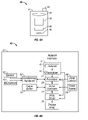
- FIG. 2 is a system block diagram illustrating one embodiment of an electronic device incorporating a 3 ⁇ 3 interferometric modulator display.
- FIG. 3 is a diagram of movable mirror position versus applied voltage for one exemplary embodiment of an interferometric modulator of FIG. 1 .
- FIG. 4 is an illustration of a set of row and column voltages that may be used to drive an interferometric modulator display.
- FIG. 5A illustrates one exemplary frame of display data in the 3 ⁇ 3 interferometric modulator display of FIG. 2 .
- FIG. 5B illustrates one exemplary timing diagram for row and column signals that may be used to write the frame of FIG. 5A .
- FIGS. 6A and 6B are system block diagrams illustrating an embodiment of a visual display device comprising a plurality of interferometric modulators.
- FIG. 7A is a cross section of the device of FIG. 1 .
- FIG. 7B is a cross section of an alternative embodiment of an interferometric modulator.
- FIG. 7C is a cross section of another alternative embodiment of an interferometric modulator.
- FIG. 7D is a cross section of yet another alternative embodiment of an interferometric modulator.
- FIG. 7E is a cross section of an additional alternative embodiment of an interferometric modulator.
- FIG. 8 depicts a front light guide unit for use in a flat panel display comprising a linear light source and a front light guide panel.
- FIG. 9 depicts a frontlit display comprising a reflective display panel, a dual film front light guide panel having embedded surface features and a light source.
- FIG. 10 depicts the top and bottom films of the dual film light guide of FIG. 9 .
- FIG. 11 depicts light rays from the display panel propagating through the light guide of FIG. 9 .
- FIG. 12 depicts light rays from ambient light propagating through the light guide to the display panel.
- FIG. 13 depicts an alternative embodiment of a front light guide wherein the distance between surface features varies across the length of the light guide.
- FIG. 14 depicts an alternative embodiment of a front light guide having embedded surface features.
- FIG. 15 depicts an alternative embodiment of a frontlit display comprising a reflective display panel, a front light guide panel having embedded surface features and a light source.
- FIG. 16 depicts an alternative embodiment of a front light guide having embedded surface features.
- FIG. 17 depicts light rays incident on one of the embedded surface features of the front light guide of FIG. 16 .
- FIG. 18 depicts an alternative embodiment of a front light guide having embedded surface features with a reflective coating.
- FIG. 19 depicts a detailed view of a portion of an alternative embodiment of a front light guide showing multifaceted embedded surface features.
- FIG. 20 depicts a detailed view of a portion of an alternative embodiment of a front light guide showing embedded surface features with curved facets.
- FIG. 21 depicts an alternative embodiment a frontlit display comprising a reflective display panel and a front light guide panel having embedded surface features, wherein the embedded surface features are disposed on a side of a film facing the light guide panel.
- FIG. 22 depicts an alternative embodiment of a frontlit display similar to that of FIG. 21 wherein the embedded surface features have vertical walls.
- an edge illuminated front light guide panel includes a plurality of embedded surface features.
- the embedded surface relief features may form fillable gaps or cavities such as air pockets within the light guide panel.
- Light injected into an edge of the light guide propagates though the light guide until it strikes an air/light guide material interface at one on the air pockets.
- the light is then turned by total internal reflection through a large angle such that it exits an output face disposed in front of a display panel.
- a pair of guide portions have contoured surfaces that are contacted to each other.
- Other embodiments are also disclosed herein.
- the embodiments may be implemented in any device that is configured to display an image, whether in motion (e.g., video) or stationary (e.g., still image), and whether textual or pictorial. More particularly, it is contemplated that the embodiments may be implemented in or associated with a variety of electronic devices such as, but not limited to, mobile telephones, wireless devices, personal data assistants (PDAs), hand-held or portable computers, GPS receivers/navigators, cameras, MP3 players, camcorders, game consoles, wrist watches, clocks, calculators, television monitors, flat panel displays, computer monitors, auto displays (e.g., odometer display, etc.), cockpit controls and/or displays, display of camera views (e.g., display of a rear view camera in a vehicle), electronic photographs, electronic billboards or signs, projectors, architectural structures, packaging, and aesthetic structures (e.g., display of images on a piece of jewelry).
- PDAs personal data assistants
- GPS receivers/navigators cameras
- the display device such as, e.g., interferometric modulating MEMS devices, LCDs, etc., may include a light source that is configured to light an array of display elements to an appropriate level for viewing.
- a light guide may be coupled to the array of display elements proximate the light source to distribute light across the array of display elements.
- Light guides may be positioned in various orientations with respect to the display elements, such as behind the display elements, e.g., a backlight, or in front of the display elements, e.g., a frontlight.
- a front light guide panel is disposed in front of the array of display elements to deliver uniform illumination from an artificial light source to the array of display elements while allowing for the option of illumination from ambient lighting via a reflective layer in the display elements.
- FIG. 1 One interferometric modulator display embodiment comprising an interferometric MEMS display element is illustrated in FIG. 1 .
- the pixels are in either a bright or dark state.
- the display element In the bright (“on” or “open”) state, the display element reflects a large portion of incident visible light to a user.
- the dark (“off” or “closed”) state When in the dark (“off” or “closed”) state, the display element reflects little incident visible light to the user.
- the light reflectance properties of the “on” and “off” states may be reversed.
- MEMS pixels can be configured to reflect predominantly at selected colors, allowing for a color display in addition to black and white.
- FIG. 1 is an isometric view depicting two adjacent pixels in a series of pixels of a visual display, wherein each pixel comprises a MEMS interferometric modulator.
- an interferometric modulator display comprises a row/column array of these interferometric modulators.
- Each interferometric modulator includes a pair of reflective layers positioned at a variable and controllable distance from each other to form a resonant optical gap with at least one variable dimension.
- one of the reflective layers may be moved between two positions. In the first position, referred to herein as the relaxed position, the movable reflective layer is positioned at a relatively large distance from a fixed partially reflective layer.
- the movable reflective layer In the second position, referred to herein as the actuated position, the movable reflective layer is positioned more closely adjacent to the partially reflective layer. Incident light that reflects from the two layers interferes constructively or destructively depending on the position of the movable reflective layer, producing either an overall reflective or non-reflective state for each pixel.
- the depicted portion of the pixel array in FIG. 1 includes two adjacent interferometric modulators 12 a and 12 b .
- a movable reflective layer 14 a is illustrated in a relaxed position at a predetermined distance from an optical stack 16 a , which includes a partially reflective layer.
- the movable reflective layer 14 b is illustrated in an actuated position adjacent to the optical stack 16 b.
- optical stack 16 typically comprise several fused layers, which can include an electrode layer, such as indium tin oxide (ITO), a partially reflective layer, such as chromium, and a transparent dielectric.
- ITO indium tin oxide
- the optical stack 16 is thus electrically conductive, partially transparent, and partially reflective, and may be fabricated, for example, by depositing one or more of the above layers onto a transparent substrate 20 .
- the partially reflective layer can be formed from a variety of materials that are partially reflective such as various metals, semiconductors, and dielectrics.
- the partially reflective layer can be formed of one or more layers of materials, and each of the layers can be formed of a single material or a combination of materials.
- the layers of the optical stack 16 are patterned into parallel strips, and may form row electrodes in a display device as described further below.
- the movable reflective layers 14 a , 14 b may be formed as a series of parallel strips of a deposited metal layer or layers (orthogonal to the row electrodes of 16 a , 16 b ) deposited on top of posts 18 and an intervening sacrificial material deposited between the posts 18 . When the sacrificial material is etched away, the movable reflective layers 14 a , 14 b are separated from the optical stacks 16 a , 16 b by a defined gap 19 .
- a highly conductive and reflective material such as aluminum may be used for the reflective layers 14 , and these strips may form column electrodes in a display device.
- the gap 19 remains between the movable reflective layer 14 a and optical stack 16 a , with the movable reflective layer 14 a in a mechanically relaxed state, as illustrated by the pixel 12 a in FIG. 1 .
- the capacitor formed at the intersection of the row and column electrodes at the corresponding pixel becomes charged, and electrostatic forces pull the electrodes together.
- the movable reflective layer 14 is deformed and is forced against the optical stack 16 .
- a dielectric layer within the optical stack 16 may prevent shorting and control the separation distance between layers 14 and 16 , as illustrated by pixel 12 b on the right in FIG. 1 .
- the behavior is the same regardless of the polarity of the applied potential difference. In this way, row/column actuation that can control the reflective vs. non-reflective pixel states is analogous in many ways to that used in conventional LCD and other display technologies.
- FIGS. 2 through 5B illustrate one exemplary process and system for using an array of interferometric modulators in a display application.
- FIG. 2 is a system block diagram illustrating one embodiment of an electronic device that may incorporate aspects of the invention.
- the electronic device includes a processor 21 which may be any general purpose single- or multi-chip microprocessor such as an ARM, Pentium®, Pentium II®, Pentium III®, Pentium IV®, Pentium® Pro, an 8051, a MIPS®, a Power PC®, an ALPHA®, or any special purpose microprocessor such as a digital signal processor, microcontroller, or a programmable gate array.
- the processor 21 may be configured to execute one or more software modules.
- the processor may be configured to execute one or more software applications, including a web browser, a telephone application, an email program, or any other software application.
- the processor 21 is also configured to communicate with an array driver 22 .
- the array driver 22 includes a row driver circuit 24 and a column driver circuit 26 that provide signals to a display array or panel 30 .
- the cross section of the array illustrated in FIG. 1 is shown by the lines 1 - 1 in FIG. 2 .
- the row/column actuation protocol may take advantage of a hysteresis property of these devices illustrated in FIG. 3 . It may require, for example, a 10 volt potential difference to cause a movable layer to deform from the relaxed state to the actuated state. However, when the voltage is reduced from that value, the movable layer maintains its state as the voltage drops back below 10 volts.
- the movable layer does not relax completely until the voltage drops below 2 volts.
- a window of applied voltage about 3 to 7 V in the example illustrated in FIG. 3 , within which the device is stable in either the relaxed or actuated state. This is referred to herein as the “hysteresis window” or “stability window.”
- the row/column actuation protocol can be designed such that during row strobing, pixels in the strobed row that are to be actuated are exposed to a voltage difference of about 10 volts, and pixels that are to be relaxed are exposed to a voltage difference of close to zero volts.
- each pixel sees a potential difference within the “stability window” of 3-7 volts in this example.
- This feature makes the pixel design illustrated in FIG. 1 stable under the same applied voltage conditions in either an actuated or relaxed pre-existing state. Since each pixel of the interferometric modulator, whether in the actuated or relaxed state, is essentially a capacitor formed by the fixed and moving reflective layers, this stable state can be held at a voltage within the hysteresis window with almost no power dissipation. Essentially no current flows into the pixel if the applied potential is fixed.
- a display frame may be created by asserting the set of column electrodes in accordance with the desired set of actuated pixels in the first row.
- a row pulse is then applied to the row 1 electrode, actuating the pixels corresponding to the asserted column lines.
- the asserted set of column electrodes is then changed to correspond to the desired set of actuated pixels in the second row.
- a pulse is then applied to the row 2 electrode, actuating the appropriate pixels in row 2 in accordance with the asserted column electrodes.
- the row 1 pixels are unaffected by the row 2 pulse, and remain in the state they were set to during the row 1 pulse. This may be repeated for the entire series of rows in a sequential fashion to produce the frame.
- the frames are refreshed and/or updated with new display data by continually repeating this process at some desired number of frames per second.
- protocols for driving row and column electrodes of pixel arrays to produce display frames are also well known and may be used in conjunction with the present invention.
- FIGS. 4 , 5 A, and 5 B illustrate one possible actuation protocol for creating a display frame on the 3 ⁇ 3 array of FIG. 2 .
- FIG. 4 illustrates a possible set of column and row voltage levels that may be used for pixels exhibiting the hysteresis curves of FIG. 3 .
- actuating a pixel involves setting the appropriate column to ⁇ V bias , and the appropriate row to + ⁇ V, which may correspond to ⁇ 5 volts and +5 volts, respectively Relaxing the pixel is accomplished by setting the appropriate column to +V bias , and the appropriate row to the same + ⁇ V, producing a zero volt potential difference across the pixel.
- the pixels are stable in whatever state they were originally in, regardless of whether the column is at +V bias , or ⁇ V bias .
- voltages of opposite polarity than those described above can be used, e.g., actuating a pixel can involve setting the appropriate column to +V bias , and the appropriate row to ⁇ V.
- releasing the pixel is accomplished by setting the appropriate column to ⁇ V bias , and the appropriate row to the same ⁇ V, producing a zero volt potential difference across the pixel.
- FIG. 5B is a timing diagram showing a series of row and column signals applied to the 3 ⁇ 3 array of FIG. 2 which will result in the display arrangement illustrated in FIG. 5A , where actuated pixels are non-reflective.
- the pixels Prior to writing the frame illustrated in FIG. 5A , the pixels can be in any state, and in this example, all the rows are at 0 volts, and all the columns are at +5 volts. With these applied voltages, all pixels are stable in their existing actuated or relaxed states.
- pixels (1,1), (1,2), (2,2), (3,2) and (3,3) are actuated.
- columns 1 and 2 are set to ⁇ 5 volts, and column 3 is set to +5 volts. This does not change the state of any pixels, because all the pixels remain in the 3-7 volt stability window.
- Row 1 is then strobed with a pulse that goes from 0, up to 5 volts, and back to zero. This actuates the (1,1) and (1,2) pixels and relaxes the (1,3) pixel. No other pixels in the array are affected.
- column 2 is set to ⁇ 5 volts
- columns 1 and 3 are set to +5 volts.
- Row 3 is similarly set by setting columns 2 and 3 to ⁇ 5 volts, and column 1 to +5 volts.
- the row 3 strobe sets the row 3 pixels as shown in FIG. 5A .
- the row potentials are zero, and the column potentials can remain at either +5 or ⁇ 5 volts, and the display is then stable in the arrangement of FIG. 5A . It will be appreciated that the same procedure can be employed for arrays of dozens or hundreds of rows and columns.
- FIGS. 6A and 6B are system block diagrams illustrating an embodiment of a display device 40 .
- the display device 40 can be, for example, a cellular or mobile telephone.
- the same components of display device 40 or slight variations thereof are also illustrative of various types of display devices such as televisions and portable media players.
- the display device 40 includes a housing 41 , a display 30 , an antenna 43 , a speaker 45 , an input device 48 , and a microphone 46 .
- the housing 41 is generally formed from any of a variety of manufacturing processes as are well known to those of skill in the art, including injection molding and vacuum forming.
- the housing 41 may be made from any of a variety of materials, including, but not limited to, plastic, metal, glass, rubber, and ceramic, or a combination thereof.
- the housing 41 includes removable portions (not shown) that may be interchanged with other removable portions of different color, or containing different logos, pictures, or symbols.
- the display 30 of exemplary display device 40 may be any of a variety of displays, including a bi-stable display, as described herein.
- the display 30 includes a flat-panel display, such as plasma, EL, OLED, STN LCD, or TFT LCD as described above, or a non-flat-panel display, such as a CRT or other tube device, as is well known to those of skill in the art.
- the display 30 includes an interferometric modulator display, as described herein.
- the components of one embodiment of exemplary display device 40 are schematically illustrated in FIG. 6B .
- the illustrated exemplary display device 40 includes a housing 41 and can include additional components at least partially enclosed therein.
- the exemplary display device 40 includes a network interface 27 that includes an antenna 43 , which is coupled to a transceiver 47 .
- the transceiver 47 is connected to a processor 21 , which is connected to conditioning hardware 52 .
- the conditioning hardware 52 may be configured to condition a signal (e.g., filter a signal).
- the conditioning hardware 52 is connected to a speaker 45 and a microphone 46 .
- the processor 21 is also connected to an input device 48 and a driver controller 29 .
- the driver controller 29 is coupled to a frame buffer 28 and to an array driver 22 , which in turn is coupled to a display array 30 .
- a power supply 50 provides power to all components as required by the particular exemplary display device 40 design.
- the network interface 27 includes the antenna 43 and the transceiver 47 so that the exemplary display device 40 can communicate with one or more devices over a network. In one embodiment, the network interface 27 may also have some processing capabilities to relieve requirements of the processor 21 .
- the antenna 43 is any antenna known to those of skill in the art for transmitting and receiving signals. In one embodiment, the antenna transmits and receives RF signals according to the IEEE 802.11 standard, including IEEE 802.11(a), (b), or (g). In another embodiment, the antenna transmits and receives RF signals according to the BLUETOOTH standard. In the case of a cellular telephone, the antenna is designed to receive CDMA, GSM, AMPS, or other known signals that are used to communicate within a wireless cell phone network.
- the transceiver 47 pre-processes the signals received from the antenna 43 so that they may be received by and further manipulated by the processor 21 .
- the transceiver 47 also processes signals received from the processor 21 so that they may be transmitted from the exemplary display device 40 via the antenna 43 .
- the transceiver 47 can be replaced by a receiver.
- network interface 27 can be replaced by an image source, which can store or generate image data to be sent to the processor 21 .
- the image source can be a digital video disc (DVD) or a hard-disc drive that contains image data, or a software module that generates image data.
- Processor 21 generally controls the overall operation of the exemplary display device 40 .
- the processor 21 receives data, such as compressed image data from the network interface 27 or an image source, and processes the data into raw image data or into a format that is readily processed into raw image data.
- the processor 21 then sends the processed data to the driver controller 29 or to frame buffer 28 for storage.
- Raw data typically refers to the information that identifies the image characteristics at each location within an image. For example, such image characteristics can include color, saturation, and gray-scale level.
- the processor 21 includes a microcontroller, CPU, or logic unit to control operation of the exemplary display device 40 .
- Conditioning hardware 52 generally includes amplifiers and filters for transmitting signals to the speaker 45 , and for receiving signals from the microphone 46 .
- Conditioning hardware 52 may be discrete components within the exemplary display device 40 , or may be incorporated within the processor 21 or other components.
- the driver controller 29 takes the raw image data generated by the processor 21 either directly from the processor 21 or from the frame buffer 28 and reformats the raw image data appropriately for high speed transmission to the array driver 22 . Specifically, the driver controller 29 reformats the raw image data into a data flow having a raster-like format, such that it has a time order suitable for scanning across the display array 30 . Then the driver controller 29 sends the formatted information to the array driver 22 .
- a driver controller 29 such as a LCD controller, is often associated with the system processor 21 as a stand-alone Integrated Circuit (IC), such controllers may be implemented in many ways. They may be embedded in the processor 21 as hardware, embedded in the processor 21 as software, or fully integrated in hardware with the array driver 22 .
- the array driver 22 receives the formatted information from the driver controller 29 and reformats the video data into a parallel set of waveforms that are applied many times per second to the hundreds and sometimes thousands of leads coming from the display's x-y matrix of pixels.
- driver controller 29 is a conventional display controller or a bi-stable display controller (e.g., an interferometric modulator controller).
- array driver 22 is a conventional driver or a bi-stable display driver (e.g., an interferometric modulator display).
- a driver controller 29 is integrated with the array driver 22 .
- display array 30 is a typical display array or a bi-stable display array (e.g., a display including an array of interferometric modulators).
- the input device 48 allows a user to control the operation of the exemplary display device 40 .
- input device 48 includes a keypad, such as a QWERTY keyboard or a telephone keypad, a button, a switch, a touch-sensitive screen, or a pressure- or heat-sensitive membrane.
- the microphone 46 is an input device for the exemplary display device 40 . When the microphone 46 is used to input data to the device, voice commands may be provided by a user for controlling operations of the exemplary display device 40 .
- Power supply 50 can include a variety of energy storage devices as are well known in the art.
- power supply 50 is a rechargeable battery, such as a nickel-cadmium battery or a lithium ion battery.
- power supply 50 is a renewable energy source, a capacitor, or a solar cell including a plastic solar cell, and solar-cell paint.
- power supply 50 is configured to receive power from a wall outlet.
- control programmability resides, as described above, in a driver controller which can be located in several places in the electronic display system. In some embodiments, control programmability resides in the array driver 22 . Those of skill in the art will recognize that the above-described optimizations may be implemented in any number of hardware and/or software components and in various configurations.
- FIGS. 7A-7E illustrate five different embodiments of the movable reflective layer 14 and its supporting structures.
- FIG. 7A is a cross section of the embodiment of FIG. 1 , where a strip of metal material 14 is deposited on orthogonally extending supports 18 .
- FIG. 7B the moveable reflective layer 14 is attached to supports at the corners only, on tethers 32 .
- FIG. 7C the moveable reflective layer 14 is suspended from a deformable layer 34 , which may comprise a flexible metal.
- the deformable layer 34 connects, directly or indirectly, to the substrate 20 around the perimeter of the deformable layer 34 .
- connection posts are herein referred to as support posts.
- the embodiment illustrated in FIG. 7D has support post plugs 42 upon which the deformable layer 34 rests.
- the movable reflective layer 14 remains suspended over the gap, as in FIGS. 7A-7C , but the deformable layer 34 does not form the support posts by filling holes between the deformable layer 34 and the optical stack 16 . Rather, the support posts are formed of a planarization material, which is used to form support post plugs 42 .
- the embodiment illustrated in FIG. 7E is based on the embodiment shown in FIG. 7D , but may also be adapted to work with any of the embodiments illustrated in FIGS. 7A-7C , as well as additional embodiments not shown. In the embodiment shown in FIG. 7E , an extra layer of metal or other conductive material has been used to form a bus structure 44 . This allows signal routing along the back of the interferometric modulators, eliminating a number of electrodes that may otherwise have had to be formed on the substrate 20 .
- the interferometric modulators function as direct-view devices, in which images are viewed from the front side of the transparent substrate 20 , the side opposite to that upon which the modulator is arranged.
- the reflective layer 14 optically shields the portions of the interferometric modulator on the side of the reflective layer opposite the substrate 20 , including the deformable layer 34 . This allows the shielded areas to be configured and operated upon without negatively affecting the image quality.
- Such shielding allows the bus structure 44 in FIG. 7E , which provides the ability to separate the optical properties of the modulator from the electromechanical properties of the modulator, such as addressing and the movements that result from that addressing.
- This separable modulator architecture allows the structural design and materials used for the electromechanical aspects and the optical aspects of the modulator to be selected and to function independently of each other.
- the embodiments shown in FIGS. 7C-7E have additional benefits deriving from the decoupling of the optical properties of the reflective layer 14 from its mechanical properties, which are carried out by the deformable layer 34 .
- This allows the structural design and materials used for the reflective layer 14 to be optimized with respect to the optical properties, and the structural design and materials used for the deformable layer 34 to be optimized with respect to desired mechanical properties.
- artificial lighting can be used to make the display visible.
- light from a source such as a fluorescent tube or LED is captured into a thin slab shaped light guide and is delivered to the display.
- the illumination can be provided by “backlighting” or “frontlighting.”
- Flat panel displays are typically “backlit” by light guide slabs (often referred to as “backlights”) that redirect light from a linear light source to transmit uniform illumination to the rear surface of the display panel.
- backlights light guide slabs
- the light injected along an edge of the light guide panel is guided within the light guide panel and extractor features located on a rear or front surface of the light guide panel can be used to disrupt the propagation of the light within the light guide panel and cause the light to be uniformly ejected across the front surface of the panel toward the display.
- flat panel reflective displays may be “front-lit” by a front light guide that delivers uniform illumination from the viewing side of the display panel. Such displays may also reflect ambient light, thereby increasing their brightness in well-lit ambient light conditions.
- the frontlight may be utilized only in low-light ambient conditions in some configurations.
- a linear source 2 such as a fluorescent tube, LED or LED array, or a light bar illuminated by an LED is injected into a thin slab shaped light guide panel 1003 located in front of the display panel 4 .
- the light 5 injected into the light guide is guided along the length of the light guide 1003 .
- the light 5 is turned through a large angle, approximately ninety degrees, such that it propagates through the thickness of the light guide 1003 and escapes through the output face 1031 .
- the light turning may be accomplished via a surface relief structure containing a plurality of turning features.
- the viewing face 1032 further contains a plurality of light turning structures such as prismatic microstructures 1040 arranged in a pattern along the width of the viewing face 1032 .
- the prismatic microstructures 1040 may comprise two or more turning facets 1042 and 1044 angled with respect to one another for reflecting the light at the facet/air interface, causing the light to be turned through a large angle.
- the plurality of pairs of adjacent facets 1042 and 1044 may comprise, for example, one shallow, long facet and a much shorter but more steeply inclined facet.
- prismatic surface relief features are either fabricated into the surface of the light guide, such as by embossing, injection molding casting or other techniques, or are fabricated into a thin film that is, in turn, attached to the surface of a planar light guide.
- the prismatic surface relief structure is located on the top surface of the light guide, i.e. the exposed surface opposite the light output face.
- the turning facets are vulnerable to contamination from dirt, water or other contaminants.
- the presence of, for example, dirt may destroy total internal reflection at the facet interface and reduces the light turning performance of the prismatic microstructure. Dust or particle contaminates trapped in the valleys of such prismatic microstructure will also scatter light directly into the viewers eye and therefore reduce display contrast.
- FIG. 9 shows an example front-lit display, comprising a linear light source 2 and a front light guide panel or plate 103 (LGP).
- This linear light source 2 may comprise, for example, a cold cathode fluorescent tube (CCFL) lamp, an LED, an OLED, a light bar illuminated by an LED or LED array, a fluorescent tube or any other suitable linear light source.
- This light source 2 is aligned parallel with an edge of the front light guide plate 103 such that light from the linear light source 2 is incident on a light-input surface 133 of the light guide plate 103 .
- CCFL cold cathode fluorescent tube
- the front light guide 103 comprises a substantially optically transmissive material capable of redirecting and uniformly redistributing light from the linear light source 2 over the planar surface of an output face.
- the light guide 103 comprises a light input surface 133 , a light output face 131 perpendicular to the light input surface, and a viewing face 132 opposite the light output face 131 .
- the light 5 from the linear light source 2 enters the light input surface 133 of the light guide plate 103 and as will be explained in more detail below, propagates along the length L of the light guide plate 103 reflecting between the front and back faces 132 and 131 of the light guide plate 103 and is turned by features within the light guide plate 103 to exit the light guide plate 103 through the light output face 131 and propagate toward the display panel 4 .
- the front light guide 103 comprises a rectangular shaped plate or sheet with the output face 131 and viewing face 132 being parallel to each other.
- the front light guide 103 may comprise a wedge shaped plate wherein the light output face 131 and viewing face 132 are angled with respect to one another.
- portions of the light output face 131 and viewing face 132 are angled with respect to one another and other portions are parallel to one another.
- the light output face 131 and viewing face 132 are not parallel to each other, for example the viewing face 132 may have a sawtooth pattern (not shown).
- the front light guide may be comprised of an upper portion and a lower portion each having contoured surfaces which are joined together such that the facing contoured surfaces create a plurality of turning features embedded between the upper and lower portions.
- the front light guide 103 may be comprised of two polymer films 136 and 138 joined together such that the light turning features 140 of the light guide 103 reside on the two adjacent faces of the polymer films 136 and 138 and are thus embedded in the resulting light guide panel 103 .
- the light guide 103 includes the bottom film 136 (positioned farther from the viewer) and the top film 138 (positioned closer to the viewer).
- the bottom film 136 has a flat planar surface that forms the output face 131 of the resulting light guide plate and an opposing structured surface 135 that includes a plurality of surface relief features 140 a spaced apart across the width of the film 136 .
- the top film 138 comprises a flat planar surface that forms the viewing face 132 of the resulting light guide 103 and an opposing structured surface 137 that includes a plurality of surface relief features 140 b spaced apart across the width of the film 138 .
- a light guide plate 103 may be created by joining the two films 136 and 138 together with their structured sides 135 and 137 facing one another such that the surface features 140 a and 104 b become embedded in the resulting film 103 and are thereby protected from outside damage or contamination.
- the films 136 and 138 are optically coupled such that when each of the structured faces 135 and 137 of the films 136 and 138 are aligned and joined together, the surface relief features 140 a and 140 b form a series of fillable gaps or cavities 150 (see FIG. 9 ) spaced apart across the length of the light guide plate 103 .
- the opposing surface features 140 a and b may not be equally spaced along the surfaces 135 and 137 of the top and bottom films 136 and 138 and may be instead intentionally offset, for example, to provide for different light turning effects along the length of the light guide plate.
- the top and bottom films 136 and 138 have the same index of refraction such that, when joined, they become optically one light guide, operating like one film, with no optical interface therebetween and a plurality of cavities embedded therein.
- the cavities may be filled with a filler material to provide mechanical stability and strength to the light guide plate.
- the filler material may have a different index of refraction from the light guide material to ensure that total internal reflection at the facet/cavity interface still occurs.
- the cavities may be open. As described above, these cavities may also be filled with material.
- the term cavity is used to describe either case, when the volume is open, e.g. filed with air or gas, and when the volume is filled with material such as an optically transmissive material having a different optical property, such as refractive index.
- the shape and size of the surface features 140 a and 140 b , and thus the resulting cavities 150 may also be chosen to interact extensively with guided light incident on the input face and to increase or maximize extraction efficiency, for example, to provide uniform distribution of light at a desired angle across the output face.
- the surface features 140 a and 140 b may comprise any suitable shape for causing light injected from the side, input face 133 that is generally parallel to the output face 131 to be turned over a large angle and ejected from the output face 131 .
- the surface features 140 a and 140 b may be shaped to permit light incident on the viewing face 132 such as ambient light that is substantially normal to the viewing face 132 to be transmitted through the light guide plate 103 and the surface features relatively unaffected and ejected from the output face 131 at an angle substantially normal to the output face.
- the surface features may comprise a plurality of repeating prismatic microstructures each comprising two adjacent, symmetrical facets.
- the surface features may comprise a plurality of repeating prismatic microstructures each comprising two adjacent facets having different angles of inclination with respect to the film. Other configurations are also possible.
- the surface features 140 a and 140 b are sufficiently small to be unobtrusive to the viewer.
- the surface features 140 a and 140 b may be identical across the length, L, of the films 136 and 138 , for example repeating the same angular orientation, shape or dimensions as described above.
- the shape, angular orientation and/or size of the surface features 140 a and b may vary across the length of the films 136 and 138 .
- the surface features 140 a may be mirror opposites of the surface features 140 b , alternatively, the surface features 140 a may be complementary shapes relative to the surface features 140 b , one fitting at least partially in the other.
- the surface features 140 a and 140 b form opposing top and bottom films 136 and 138 may create a plurality of symmetrical cavities 150 embedded in between the two films.
- the surface features 140 a and 140 b from opposing top and bottom films 136 and 138 may create asymmetrical cavities embedded between the films.
- such asymmetrical cavities may be designed to reduce the length of the facet/air interface and thereby reduce the detrimental Fresnel reflections that occur when the light rays strike the interface.
- re-entrant structures may be created where the re-entrant nature is not formed in either film, but rather is created when the surface features 140 a and 140 b of the top and bottom films 136 and 138 are joined.
- the surface features 140 a on the bottom film 136 comprise a plurality of alternating microprisms 142 spaced apart across the length of the structured surface 135 and separated by a plurality of planar spacers 143 .
- the microprisms 142 are formed of adjacent facets angled with respect to each other such that light rays 5 incident on the tip of the microprisms 142 will enter the prism and subsequently be internally reflected at the microprism/air interface and thereby turned through a large angle to be ejected from the output face 131 of the light guide 103 as light rays 6 .
- the surface features 140 b on the top film 138 comprise a plurality of grooves 144 spaced apart across the length of the structured surface 137 .
- the grooves 144 comprise adjacent angled surfaces, having angles with respect to one another such that total internal reflection (TIR) rays that are totally internally reflected across the length of the film 138 , as well light rays with angles close to TIR, incident on the grooves 144 will be refracted straight across the width of the grooves 144 .
- TIR total internal reflection
- These cavities 150 create an air/light guide material interface at the surface of the microprisms 142 which causes the light traveling through the tip of the microprisms 142 to be turned through a large angle, thus redistributing and redirecting light rays incident 5 on the input face 133 to be ejected as light 6 through the output face 131 and toward the display 4 .
- TIR total internal reflection
- the light rays 5 are turned through a large angle and ejected from the light output face 131 of the light guide plate 103 .
- the light rays 6 ejected from the light output face 131 of the light guide plate 103 propagate across an air gap and are incident on the display panel 4 , for example an interferometric modulator display panel, wherein the rays are modulated and reflected back toward the light output face 131 of the light guide.
- the modulated light rays 7 from the display panel 4 are incident on light output face 131 of the light guide plate 103 .
- the surface features 140 a and 140 b , and thus cavities 150 are shaped such that light incident upon the light output face 131 at normal or near normal angles is transmitted through the light guide plate 103 and the cavities 150 without much disturbance or deviation.
- the ambient light rays 8 incident on the viewing face 132 at a normal or near normal angle are likewise propagated through the light guide plate 103 and cavities 150 without much disturbance.
- the ambient light rays 8 are then ejected from the light output face 131 and propagate across an air gap to the display 4 as described above.
- the light guide plate 103 provides the capability to interact extensively with the guided light incident on a light input face while at the same time only slightly disturbing non-guided light incident on the output and viewing faces.
- the light guide plate 103 provides protection for the light turning features from damage or contamination by embedding the surface features in between two films.
- the size, shape spacing, or other characteristic of the surface features 140 a and b may be varied across the length, L, of the light guide plate 103 , for example to obtain uniform light extraction across the length of the light output face 131 .
- a particular light guide panel 103 (as illustrated in FIGS. 9-12 ) is shown with the distance between pairs of corresponding surface features 140 a and 140 b varying from 50 to 450 microns across the width of the light guide plate.
- the spacing between surface features 140 a and 140 b decreases with increasing distance from the light source 2 .
- the spacing between pairs of surface features 140 a and 140 b is about 450 microns; in the middle region B the spacing between pairs of surface features 140 a and 140 b is about 150 microns; and in the farthest region C the spacing between pairs of surface features 140 a and 140 b is about 50 microns.
- the decrease in distance between the pairs of surface features 140 a and 140 b results in an increase in extraction efficiency in the regions of the light guide plate 103 furthest from the light source 2 . This extraction efficiency balances out the decrease in light flux actually reaching father regions of the light guide 103 and results in a more uniform output across the surface of the light output face 131 .
- the viewing face 132 , of the light guide plate 103 may be angled with respect to the output face 131 to form a wedged shaped light guide plate 103 which also increases the extraction efficiency in the regions of light guide plate furthest from the light source 2 .
- the light guide 103 may be fabricated by imprinting films 136 and 138 with a designed surface relief, such as the microprisms 142 on bottom film 136 or the faceted grooves 144 on top film 136 depicted in FIG. 10 . These surface relief features may be created by embossing, injection molding or any other suitable technique known in the art. Once the surface features have been molded on the top and bottom films, the films may be aligned and joined together to create the light guide plate 103 . The films may be joined together, for example, by laminating with any suitable adhesive. Suitable adhesives may include pressure sensitive adhesives, heat cured adhesives, UV or electron beam cured adhesives or any other adhesives having suitable optical and mechanical properties.
- the films when laminating the films, however, care must be taken not to fill the open cavities between the surface features with the adhesive material, thereby possibly destroying the light turning properties of the cavities.
- the films are between about 70-80 microns thick, however the surface features are only between about 7 to 8 microns deep. Therefore, without due care, the laminating adhesive used to join the top and bottom films may ooze or seep into and fill the open cavities created by the surface features when pressure is applied to join the films. This result may be avoided by controlling the thickness of the laminating material applied between the top and bottom films to prevent excess adhesive.
- a photo-reactive adhesive may be used and may be cured by UV light so that excessive pressure on the two films is not required to join the two films.
- a thin metallic coating may be applied between the two films and then cured with RF energy.
- the laminating material may be applied before the films are imprinted with surface relief features. When the surface features are imprinted on each film, the laminating material will be removed from the surface features and thus when the two films are joined there will not be any excess material to seep into the open cavities.
- the open cavities may be filled with a filler material having a lower refractive index than the light guide material. This filler material may be added prior to laminating such that the filler material serves the added function of preventing any of the laminating material from seeping into and filling the cavities.
- the turning features embedded in the light guide may be created by a single contoured film laminated to a planar film.
- a light guide 203 may comprise a single contoured film 238 laminated to the top, planar surface of light guide plate 223 , such as a plastic or glass light guide.
- the contour surface of the film 238 is farther from the display panel than the planar surface.
- the turning facets may be protected by applying a planar plastic cover layer 260 to the contoured surface of film 238 .
- the film 238 may comprise a plastic film, such as acrylic, polycarbonate, ZEONEX® or any other suitable plastic known in the art.
- the film 238 may be imprinted with a repeating surface relief structure created by embossing, injection molding or any other suitable technologies.
- the surface relief features 240 may comprise a plurality of facets 242 and 244 , which may be either be symmetric or asymmetric.
- the film 238 may then be attached or laminated to the top surface of a light guide plate 223 such that the embossed film 238 effectively becomes part of the light guide plate 223 .
- Index matching adhesive may be used.
- the imprinted surface relief features 240 remain as the top, exposed surface of the film 238 .
- a cover layer 260 is then attached or laminated to the exposed surface of the film 238 . As discussed above, if the refractive index of both the film 238 and the cover layer 260 are similar, the surface relief features 240 are effectively embedded in the composite (single unitary) light guide 203 .
- cavities 250 are created between the surface relief features 240 and the cover layer 260 .
- plural light rays 5 from the light source 2 enter the light guide 203 at a light input surface 233 and are guided along the length of the light guide via total internal reflection of the rays at the interface between the light guide 203 and the surrounding air.
- a light ray 5 strikes the light guide material/air interface created by one of the embedded cavities 250 at an angle greater than the critical angle for total internal reflection, the light ray 5 will likewise undergo total internal reflection.
- the total internally reflected light is turned through a large angle, usually ninety degrees or greater and may then exit the light guide 203 via the light output face 231 towards the display panel 4 .
- the surface relief features 340 may be configured such that the cavities (e.g., air pockets) 350 in the light guide 303 have an asymmetrical shape.
- the side closer to the light source 2 is different than the side farther from the light source 2 .
- the steepness of the two facets 342 and 344 is different.
- the surface relief features 340 comprises two adjoining facets 342 and 344 wherein the first facet 342 is a short, steep facet and the second facet 344 is a vertical facet.
- the asymmetrical shape of the cavities 350 reduces the length of the light guide material/air interface and thereby reduces the detrimental Fresnel reflections that occur when light strikes the interface.
- the facets may have other angles as well, and may be shaped differently.
- a further advantage of the embedded surface relief features is that the use of embedded air/light guide material interfaces formed by the cavities 350 more efficiently relays light 5 from a side light source 2 .
- a side light source 2 For example, as shown in FIG. 17 , when light rays 5 contained within a cone having a half angle of approximately 30° propagate through the light guide 303 and strike the light guide material/air interface at an cavities 350 , some of the light 6 is turned down by total internal reflection, as described above, while some of the light 7 is refracted through the interface into the cavities 350 .
- the light 7 may propagate through the cavities 350 until it strikes air/light guide material interface at the vertical facet 344 . The light 7 is then refracted at this interface and is thereby quasi-collimated back into the light guide material.
- the efficiency of the light guide is improved by embedding the cavities and providing a second air/light guide material interface to prevent some refracted light from escaping the light guide.
- the turning facets 242 and 244 may be coated with a reflective coating 280 such as silver or any other suitable metallic coating.
- the reflective coating 280 may also improve the efficiency of the light guide, by causing any light that would have previously been refracted through the light guide material/air interface instead of being turned via total internal reflection to be reflected downward to the display panel by the reflective coating.
- the cavities 250 may also be filled with a filler material to provide mechanical stability and strength to the structure.
- the filler material may be reflective.
- the turning facets 242 and 244 may be any suitable shape for causing the light to turn over a large angle at the light guide material/air interface created by the surface features 240 .
- the size, shape, spacing or other characteristics of the facets may be varied to obtain uniform light extraction across the length of the light guide 203 .
- the surface relief features 240 may comprise a plurality of multifaceted surfaces 442 and 444 instead of the single faceted surfaces 242 and 244 as shown in FIG. 15 .
- the multifaceted surfaces may increase the angular range over which the incident light is turned and thus increase the probability that light turned by adjacent surface features 240 , such as shown in FIG.
- the turning surfaces 542 and 544 may alternatively comprise a single curved surface.
- the curved surfaces 542 and 544 may provide the same advantages as discussed above by varying the interface angle of the air/light guide material interface depending upon the location at which the incident light strikes the turning facet 542 and 544 . This in turn increases the angular range over which the light is totally internally reflected and thereby increases the probability that light reflected by adjacent surface features 240 will overlap as it strikes the display panel 4 , thus improving the uniformity of the light incident on the display panel 4 .
- the composite light guide 603 may comprise a film 638 having a first planar surface and a second contoured surface with concave surface relief features 640 extending across the length of a first side of the film and a plastic or glass light guide plate 623 having top and bottom planar surfaces.
- the film 638 may be attached or laminated to the bottom surface of the light guide plate 623 such that the planar surface of the film 638 is adjacent to the planar bottom surface of the light guide and the film 638 effectively becomes part of the light guide plate 623 .
- the contoured surface of the film 638 faces away from the light guide plate 623 such that the concave surface relief features 640 remain on the exposed surface of the film 638 , also facing away from the light guide plate 623 .
- the concave surface features 640 may be protected by applying a planar plastic cover layer 660 to the contoured surface of film 638 to embed the surface features between the film 638 and the cover layer 660 . As discussed above, if the refractive index of both the film 638 and the cover layer 660 are similar, the surface relief features 640 are effectively embedded in the composite light guide 603 .
- the concave surface of the film 638 may be attached or laminated directly to the array of display elements such that the concave surface features are embedded between the film 638 and the array of display elements.
- the concave surface relief features 640 may comprise a plurality of adjacent facets which may be either be symmetric or asymmetric.
- the concave surface relief features 640 comprise sloping side walls or facets 642 and 644 having the same slope although the slopes can be different in different embodiments. These sloping side walls 642 and 644 are tilted such that the cavity 650 widens with depth into the film 638 .
- the edges of each facet 642 and 644 nearest the display elements 4 are closer to each other than the edges of each facet 642 and 644 furthest from the display.
- the surface relief features 640 may be shaped and sized such that guided light propagating through the light guide 603 will be totally internally reflected at the air/light guide material interface.
- plural light rays 5 from the light source 2 enter the light guide 603 at a light input surface 633 and are guided along the length of the light guide via total internal reflection of the rays at the interface between the light guide 603 and the surrounding air.
- a light ray 5 strikes the air/light guide material interface created by one of the embedded cavities (e.g., air pockets) 650 at an angle greater than the critical angle for total internal reflection, the light ray 5 will undergo total internal reflection at the facet 642 .
- the total internally reflected light is turned through a large angle, usually ninety degrees or greater (relative to the light output face 631 ) and may then exit the light guide 603 via the light output face 631 towards the array of display elements 4 .
- the surface relief features 740 may be shaped and sized such that guided light propagating through the light guide 703 will be turned towards the array of display elements by refraction of the light rays at the air/light guide material interface. Cavities (e.g., air pockets) 750 , similar to the cavities discussed above, are created between the surface relief features 740 and the cover layer 760 .
- the surface relief features 740 comprise vertical sidewalls or facets 742 and 744 , although the shapes may be different in different embodiments.
- light rays 5 from the light source 2 enter the light guide 703 at a light input surface 733 and are guided along the length of the light guide via total internal reflection of the rays at the interface between the light guide 503 and the surrounding air.
- the light ray 5 strikes the air/light guide material interface created by one of the embedded cavities 750 , the light ray 5 will be refracted due to the change in refractive index between the light guide and air. Because of the angle of air/light guide material interface created by the facet 742 of the surface relief features 740 , the light will be bent such that it exits the light guide 703 via the light output face 731 and is directed towards the array of display elements 4 .
- Structural features may be added, removed, reordered, or rearranged. Different structural features may be substituted out. The type, arrangement, and configuration of the components may be different. Components may be added or removed. Similarly, processing steps may be added or removed, or reordered. Also, although some embodiments are described as plates, these embodiments may otherwise comprise films or sheets. Additionally, the terms film and layer as used herein include film stacks and multilayers. While these embodiments are discussed in the context of an interferometric display, one of skill in the art will recognize that the technology is applicable in any directed-lighting solution including room lighting and display lighting for any of reflective, transmissive and transflective technologies.
Landscapes
- Physics & Mathematics (AREA)
- General Physics & Mathematics (AREA)
- Optics & Photonics (AREA)
- Spectroscopy & Molecular Physics (AREA)
- Nonlinear Science (AREA)
- Crystallography & Structural Chemistry (AREA)
- Chemical & Material Sciences (AREA)
- Mathematical Physics (AREA)
- Mechanical Light Control Or Optical Switches (AREA)
- Planar Illumination Modules (AREA)
- Light Guides In General And Applications Therefor (AREA)
- Liquid Crystal (AREA)
- Micromachines (AREA)
Abstract
Description
Claims (24)
Priority Applications (17)
| Application Number | Priority Date | Filing Date | Title |
|---|---|---|---|
| US11/742,299 US7733439B2 (en) | 2007-04-30 | 2007-04-30 | Dual film light guide for illuminating displays |
| EP08153436A EP1988332A1 (en) | 2007-04-30 | 2008-03-27 | Dual film light guide for illuminating displays |
| EP08153770A EP1988333A1 (en) | 2007-04-30 | 2008-03-31 | Dual film light guide for illuminating displays |
| RU2009140154/28A RU2482387C2 (en) | 2007-04-30 | 2008-04-21 | Double film lightguide for display highlighting |
| CN2011102774624A CN102354012A (en) | 2007-04-30 | 2008-04-21 | Dual film light guide for illuminating displays |
| PCT/US2008/061046 WO2008137299A1 (en) | 2007-04-30 | 2008-04-21 | Dual film light guide for illuminating displays |
| CN2008800142560A CN101675295B (en) | 2007-04-30 | 2008-04-21 | Dual film light guides for illuminating displays |
| BRPI0810811A BRPI0810811A2 (en) | 2007-04-30 | 2008-04-21 | light guide and method of manufacture |
| JP2010506419A JP2010526341A (en) | 2007-04-30 | 2008-04-21 | Double membrane light guide for illuminating the display |
| KR1020097024794A KR20100036233A (en) | 2007-04-30 | 2008-04-21 | Dual film light guide for illuminating displays |
| CA002685682A CA2685682A1 (en) | 2007-04-30 | 2008-04-21 | Dual film light guide for illuminating displays |
| TW097115999A TWI595293B (en) | 2007-04-30 | 2008-04-30 | Dual film light guide for illuminated displays |
| US12/725,407 US20100231510A1 (en) | 2007-04-30 | 2010-03-16 | Dual film light guide for illuminating displays |
| US12/795,542 US8373821B2 (en) | 2007-04-30 | 2010-06-07 | Dual film light guide for illuminating displays |
| JP2012204275A JP2013011904A (en) | 2007-04-30 | 2012-09-18 | Dual film light guide for illuminating displays |
| US14/451,489 US9054056B2 (en) | 2007-04-30 | 2014-08-05 | Transistor performance using a two-step damage anneal |
| US14/451,485 US9029251B2 (en) | 2007-04-30 | 2014-08-05 | Transistor performance using a two-step damage anneal |
Applications Claiming Priority (1)
| Application Number | Priority Date | Filing Date | Title |
|---|---|---|---|
| US11/742,299 US7733439B2 (en) | 2007-04-30 | 2007-04-30 | Dual film light guide for illuminating displays |
Related Child Applications (2)
| Application Number | Title | Priority Date | Filing Date |
|---|---|---|---|
| US12/725,407 Division US20100231510A1 (en) | 2007-04-30 | 2010-03-16 | Dual film light guide for illuminating displays |
| US12/795,542 Continuation US8373821B2 (en) | 2007-04-30 | 2010-06-07 | Dual film light guide for illuminating displays |
Publications (2)
| Publication Number | Publication Date |
|---|---|
| US20080267572A1 US20080267572A1 (en) | 2008-10-30 |
| US7733439B2 true US7733439B2 (en) | 2010-06-08 |
Family
ID=39712710
Family Applications (3)
| Application Number | Title | Priority Date | Filing Date |
|---|---|---|---|
| US11/742,299 Active US7733439B2 (en) | 2007-04-30 | 2007-04-30 | Dual film light guide for illuminating displays |
| US12/725,407 Abandoned US20100231510A1 (en) | 2007-04-30 | 2010-03-16 | Dual film light guide for illuminating displays |
| US12/795,542 Active 2027-10-16 US8373821B2 (en) | 2007-04-30 | 2010-06-07 | Dual film light guide for illuminating displays |
Family Applications After (2)
| Application Number | Title | Priority Date | Filing Date |
|---|---|---|---|
| US12/725,407 Abandoned US20100231510A1 (en) | 2007-04-30 | 2010-03-16 | Dual film light guide for illuminating displays |
| US12/795,542 Active 2027-10-16 US8373821B2 (en) | 2007-04-30 | 2010-06-07 | Dual film light guide for illuminating displays |
Country Status (10)
| Country | Link |
|---|---|
| US (3) | US7733439B2 (en) |
| EP (2) | EP1988332A1 (en) |
| JP (2) | JP2010526341A (en) |
| KR (1) | KR20100036233A (en) |
| CN (2) | CN102354012A (en) |
| BR (1) | BRPI0810811A2 (en) |
| CA (1) | CA2685682A1 (en) |
| RU (1) | RU2482387C2 (en) |
| TW (1) | TWI595293B (en) |
| WO (1) | WO2008137299A1 (en) |
Cited By (42)
| Publication number | Priority date | Publication date | Assignee | Title |
|---|---|---|---|---|
| US20040207774A1 (en) * | 2003-04-17 | 2004-10-21 | Gothard David L. | Illumination apparatus for LCD/organic displays |
| US20090140962A1 (en) * | 2006-08-17 | 2009-06-04 | Hyun Ha Hwang | Display Device and Mobile Terminal Having the Same |
| US20090255569A1 (en) * | 2008-04-11 | 2009-10-15 | Qualcomm Mems Technologies, Inc. | Method to improve pv aesthetics and efficiency |
| US20090296193A1 (en) * | 2008-05-28 | 2009-12-03 | Qualcomm Mems Technologies, Inc. | Front Light Devices and Methods of Fabrication Thereof |
| US20100141557A1 (en) * | 2006-10-06 | 2010-06-10 | Qualcomm Mems Technologies, Inc. | Light guide |
| US20100149624A1 (en) * | 2004-09-27 | 2010-06-17 | Qualcomm Mems Technologies, Inc. | Method and device for compensating for color shift as a function of angle of view |
| US20100157587A1 (en) * | 2008-12-23 | 2010-06-24 | Hiroto Isoda | Light-emitting unit and electronic device using the same |
| US20100172012A1 (en) * | 2004-09-27 | 2010-07-08 | Idc, Llc | System and method of reducing color shift in a display |
| US20100231510A1 (en) * | 2007-04-30 | 2010-09-16 | Qualcomm Mems Technologies, Inc. | Dual film light guide for illuminating displays |
| US7845841B2 (en) | 2006-08-28 | 2010-12-07 | Qualcomm Mems Technologies, Inc. | Angle sweeping holographic illuminator |
| US7864395B2 (en) | 2006-10-27 | 2011-01-04 | Qualcomm Mems Technologies, Inc. | Light guide including optical scattering elements and a method of manufacture |
| US7907319B2 (en) | 1995-11-06 | 2011-03-15 | Qualcomm Mems Technologies, Inc. | Method and device for modulating light with optical compensation |
| US20110157058A1 (en) * | 2009-12-29 | 2011-06-30 | Qualcomm Mems Technologies, Inc. | Coated light-turning feature with auxiliary structure |
| US20110169428A1 (en) * | 2010-01-08 | 2011-07-14 | Qualcomm Mems Technologies, Inc. | Edge bar designs to mitigate edge shadow artifact |
| US8040589B2 (en) | 2008-02-12 | 2011-10-18 | Qualcomm Mems Technologies, Inc. | Devices and methods for enhancing brightness of displays using angle conversion layers |
| US8045252B2 (en) | 2004-02-03 | 2011-10-25 | Qualcomm Mems Technologies, Inc. | Spatial light modulator with integrated optical compensation structure |
| US8049951B2 (en) | 2008-04-15 | 2011-11-01 | Qualcomm Mems Technologies, Inc. | Light with bi-directional propagation |
| US8061882B2 (en) | 2006-10-06 | 2011-11-22 | Qualcomm Mems Technologies, Inc. | Illumination device with built-in light coupler |
| US8068710B2 (en) * | 2007-12-07 | 2011-11-29 | Qualcomm Mems Technologies, Inc. | Decoupled holographic film and diffuser |
| US8107155B2 (en) | 2006-10-06 | 2012-01-31 | Qualcomm Mems Technologies, Inc. | System and method for reducing visual artifacts in displays |
| US8231257B2 (en) | 2009-01-13 | 2012-07-31 | Qualcomm Mems Technologies, Inc. | Large area light panel and screen |
| US8300304B2 (en) | 2008-02-12 | 2012-10-30 | Qualcomm Mems Technologies, Inc. | Integrated front light diffuser for reflective displays |
| US8358266B2 (en) | 2008-09-02 | 2013-01-22 | Qualcomm Mems Technologies, Inc. | Light turning device with prismatic light turning features |
| US8368981B2 (en) | 2006-10-10 | 2013-02-05 | Qualcomm Mems Technologies, Inc. | Display device with diffractive optics |
| US8402647B2 (en) | 2010-08-25 | 2013-03-26 | Qualcomm Mems Technologies Inc. | Methods of manufacturing illumination systems |
| US20130314943A1 (en) * | 2012-05-22 | 2013-11-28 | Jiandong Huang | Waveguide with Controlled Light Collimation |
| US8596846B2 (en) | 2012-03-16 | 2013-12-03 | Nano-Optic Devices, Llc | Frontlight unit for enhancing illumination of a reflective display |
| US8630518B2 (en) * | 2012-05-22 | 2014-01-14 | Sharp Laboratories Of America, Inc. | Ultra-thin waveguide with controlled light extraction |
| US8654061B2 (en) | 2008-02-12 | 2014-02-18 | Qualcomm Mems Technologies, Inc. | Integrated front light solution |
| US8902484B2 (en) | 2010-12-15 | 2014-12-02 | Qualcomm Mems Technologies, Inc. | Holographic brightness enhancement film |
| US8928967B2 (en) | 1998-04-08 | 2015-01-06 | Qualcomm Mems Technologies, Inc. | Method and device for modulating light |
| US8971675B2 (en) | 2006-01-13 | 2015-03-03 | Qualcomm Mems Technologies, Inc. | Interconnect structure for MEMS device |
| US8979349B2 (en) | 2009-05-29 | 2015-03-17 | Qualcomm Mems Technologies, Inc. | Illumination devices and methods of fabrication thereof |
| US9019183B2 (en) | 2006-10-06 | 2015-04-28 | Qualcomm Mems Technologies, Inc. | Optical loss structure integrated in an illumination apparatus |
| US9025235B2 (en) | 2002-12-25 | 2015-05-05 | Qualcomm Mems Technologies, Inc. | Optical interference type of color display having optical diffusion layer between substrate and electrode |
| US9110289B2 (en) | 1998-04-08 | 2015-08-18 | Qualcomm Mems Technologies, Inc. | Device for modulating light with multiple electrodes |
| US9164219B2 (en) | 2011-11-14 | 2015-10-20 | Nano-Optic Devices, Llc | Frontlight unit for reflective displays |
| US9348082B2 (en) | 2011-03-08 | 2016-05-24 | Dolby Laboratories Licensing Corporation | Illuminator for reflective displays |
| US9703086B1 (en) * | 2015-12-30 | 2017-07-11 | Orangetek Corporation | Beam splitter |
| US10216285B2 (en) | 2015-02-02 | 2019-02-26 | Microsoft Technology Licensing, Llc | Backlit illumination of electronics |
| US10310166B2 (en) * | 2015-04-10 | 2019-06-04 | Japan Display Inc. | Display device, lightguide plate, and manufacturing method thereof |
| US20210396925A1 (en) * | 2020-03-24 | 2021-12-23 | Hangzhou Xineng New Material Co., Ltd. | Light guide film, production method thereof and light guide device |
Families Citing this family (123)
| Publication number | Priority date | Publication date | Assignee | Title |
|---|---|---|---|---|
| US7706050B2 (en) | 2004-03-05 | 2010-04-27 | Qualcomm Mems Technologies, Inc. | Integrated modulator illumination |
| US7750886B2 (en) | 2004-09-27 | 2010-07-06 | Qualcomm Mems Technologies, Inc. | Methods and devices for lighting displays |
| US7603001B2 (en) | 2006-02-17 | 2009-10-13 | Qualcomm Mems Technologies, Inc. | Method and apparatus for providing back-lighting in an interferometric modulator display device |
| US7766498B2 (en) | 2006-06-21 | 2010-08-03 | Qualcomm Mems Technologies, Inc. | Linear solid state illuminator |
| US7855827B2 (en) | 2006-10-06 | 2010-12-21 | Qualcomm Mems Technologies, Inc. | Internal optical isolation structure for integrated front or back lighting |
| US7777954B2 (en) | 2007-01-30 | 2010-08-17 | Qualcomm Mems Technologies, Inc. | Systems and methods of providing a light guiding layer |
| TWI382551B (en) * | 2008-11-06 | 2013-01-11 | Ind Tech Res Inst | Solar collector module |
| US9743486B2 (en) * | 2009-10-30 | 2017-08-22 | E Ink Holdings Inc. | Electronic device |
| KR101104141B1 (en) * | 2009-11-30 | 2012-01-13 | 한국과학기술원 | Light Guide Plates and Backlight Units |
| KR101311304B1 (en) * | 2009-12-15 | 2013-09-25 | 엘지디스플레이 주식회사 | Transparent display device |
| AU2011237540B2 (en) | 2010-04-06 | 2015-05-07 | Nitto Denko Corporation | Laminate structure with embedded cavities and related method of manufacture |
| US20110244187A1 (en) * | 2010-04-06 | 2011-10-06 | Modilis Holdings Llc | Internal Cavity Optics |
| US9082566B2 (en) | 2010-09-02 | 2015-07-14 | Blackberry Limited | Backlighting assembly for a keypad |
| US8431849B2 (en) | 2010-09-24 | 2013-04-30 | Research In Motion Limited | Backlighting apparatus for a keypad assembly |
| US9201185B2 (en) | 2011-02-04 | 2015-12-01 | Microsoft Technology Licensing, Llc | Directional backlighting for display panels |
| EP2681730B1 (en) * | 2011-03-02 | 2022-08-17 | Stratacache, Inc. | Door including a translucent digital display system |
| US9881528B2 (en) | 2011-10-13 | 2018-01-30 | Manufacturing Resources International, Inc. | Transparent liquid crystal display on display case |
| US9223138B2 (en) | 2011-12-23 | 2015-12-29 | Microsoft Technology Licensing, Llc | Pixel opacity for augmented reality |
| US8789995B2 (en) * | 2012-01-06 | 2014-07-29 | Qualcomm Mems Technologies, Inc. | Light guide with at least partially non-transmissive coating on ledge region |
| US9606586B2 (en) | 2012-01-23 | 2017-03-28 | Microsoft Technology Licensing, Llc | Heat transfer device |
| US9354748B2 (en) | 2012-02-13 | 2016-05-31 | Microsoft Technology Licensing, Llc | Optical stylus interaction |
| US9297996B2 (en) | 2012-02-15 | 2016-03-29 | Microsoft Technology Licensing, Llc | Laser illumination scanning |
| US9368546B2 (en) | 2012-02-15 | 2016-06-14 | Microsoft Technology Licensing, Llc | Imaging structure with embedded light sources |
| US9726887B2 (en) | 2012-02-15 | 2017-08-08 | Microsoft Technology Licensing, Llc | Imaging structure color conversion |
| US9779643B2 (en) | 2012-02-15 | 2017-10-03 | Microsoft Technology Licensing, Llc | Imaging structure emitter configurations |
| US9158383B2 (en) | 2012-03-02 | 2015-10-13 | Microsoft Technology Licensing, Llc | Force concentrator |
| US9075566B2 (en) | 2012-03-02 | 2015-07-07 | Microsoft Technoogy Licensing, LLC | Flexible hinge spine |
| US9360893B2 (en) | 2012-03-02 | 2016-06-07 | Microsoft Technology Licensing, Llc | Input device writing surface |
| US9064654B2 (en) | 2012-03-02 | 2015-06-23 | Microsoft Technology Licensing, Llc | Method of manufacturing an input device |
| US9870066B2 (en) | 2012-03-02 | 2018-01-16 | Microsoft Technology Licensing, Llc | Method of manufacturing an input device |
| US8873227B2 (en) | 2012-03-02 | 2014-10-28 | Microsoft Corporation | Flexible hinge support layer |
| US9298236B2 (en) | 2012-03-02 | 2016-03-29 | Microsoft Technology Licensing, Llc | Multi-stage power adapter configured to provide a first power level upon initial connection of the power adapter to the host device and a second power level thereafter upon notification from the host device to the power adapter |
| US9426905B2 (en) | 2012-03-02 | 2016-08-23 | Microsoft Technology Licensing, Llc | Connection device for computing devices |
| USRE48963E1 (en) | 2012-03-02 | 2022-03-08 | Microsoft Technology Licensing, Llc | Connection device for computing devices |
| US9578318B2 (en) | 2012-03-14 | 2017-02-21 | Microsoft Technology Licensing, Llc | Imaging structure emitter calibration |
| US11068049B2 (en) | 2012-03-23 | 2021-07-20 | Microsoft Technology Licensing, Llc | Light guide display and field of view |
| US9558590B2 (en) | 2012-03-28 | 2017-01-31 | Microsoft Technology Licensing, Llc | Augmented reality light guide display |
| US10191515B2 (en) | 2012-03-28 | 2019-01-29 | Microsoft Technology Licensing, Llc | Mobile device light guide display |
| US9717981B2 (en) | 2012-04-05 | 2017-08-01 | Microsoft Technology Licensing, Llc | Augmented reality and physical games |
| US20130300590A1 (en) | 2012-05-14 | 2013-11-14 | Paul Henry Dietz | Audio Feedback |
| US10502876B2 (en) | 2012-05-22 | 2019-12-10 | Microsoft Technology Licensing, Llc | Waveguide optics focus elements |
| US8989535B2 (en) | 2012-06-04 | 2015-03-24 | Microsoft Technology Licensing, Llc | Multiple waveguide imaging structure |
| US8947353B2 (en) | 2012-06-12 | 2015-02-03 | Microsoft Corporation | Photosensor array gesture detection |
| US9684382B2 (en) | 2012-06-13 | 2017-06-20 | Microsoft Technology Licensing, Llc | Input device configuration having capacitive and pressure sensors |
| US9459160B2 (en) | 2012-06-13 | 2016-10-04 | Microsoft Technology Licensing, Llc | Input device sensor configuration |
| US9256089B2 (en) | 2012-06-15 | 2016-02-09 | Microsoft Technology Licensing, Llc | Object-detecting backlight unit |
| US8964379B2 (en) | 2012-08-20 | 2015-02-24 | Microsoft Corporation | Switchable magnetic lock |
| EP2897516B1 (en) | 2012-09-24 | 2017-12-13 | Invuity, Inc. | Apparatus for controlling optical properties of light |
| US8654030B1 (en) | 2012-10-16 | 2014-02-18 | Microsoft Corporation | Antenna placement |
| CN104870123B (en) | 2012-10-17 | 2016-12-14 | 微软技术许可有限责任公司 | Metal alloy injection shaped projection |
| TWI475309B (en) * | 2012-11-06 | 2015-03-01 | Wistron Corp | Electronic paper display |
| US10192358B2 (en) | 2012-12-20 | 2019-01-29 | Microsoft Technology Licensing, Llc | Auto-stereoscopic augmented reality display |
| CN103912797A (en) * | 2013-01-06 | 2014-07-09 | 纬创资通股份有限公司 | Backlight module |
| KR101425372B1 (en) * | 2013-01-23 | 2014-08-06 | (주)애니캐스팅 | Light guide plate and back light unit including the same |
| US10578499B2 (en) | 2013-02-17 | 2020-03-03 | Microsoft Technology Licensing, Llc | Piezo-actuated virtual buttons for touch surfaces |
| KR101425983B1 (en) * | 2013-03-05 | 2014-08-05 | (주)애니캐스팅 | Light guide plate and method for manufacturing the same |
| US9448631B2 (en) | 2013-12-31 | 2016-09-20 | Microsoft Technology Licensing, Llc | Input device haptics and pressure sensing |
| US9759854B2 (en) | 2014-02-17 | 2017-09-12 | Microsoft Technology Licensing, Llc | Input device outer layer and backlighting |
| US9423552B2 (en) | 2014-02-24 | 2016-08-23 | Google Inc. | Lightguide device with outcoupling structures |
| US10120420B2 (en) | 2014-03-21 | 2018-11-06 | Microsoft Technology Licensing, Llc | Lockable display and techniques enabling use of lockable displays |
| US9535293B2 (en) | 2014-06-16 | 2017-01-03 | Manufacturing Resources International, Inc. | Sealed transparent liquid crystal display assembly |
| US9500896B2 (en) | 2014-06-16 | 2016-11-22 | Manufacturing Resources International, Inc. | Cooling system for liquid crystal display |
| US9633366B2 (en) | 2014-06-16 | 2017-04-25 | Manufacturing Resources International, Inc. | System for tracking and analyzing display case usage |
| US10324733B2 (en) | 2014-07-30 | 2019-06-18 | Microsoft Technology Licensing, Llc | Shutdown notifications |
| US9304235B2 (en) | 2014-07-30 | 2016-04-05 | Microsoft Technology Licensing, Llc | Microfabrication |
| US10254942B2 (en) | 2014-07-31 | 2019-04-09 | Microsoft Technology Licensing, Llc | Adaptive sizing and positioning of application windows |
| US10678412B2 (en) | 2014-07-31 | 2020-06-09 | Microsoft Technology Licensing, Llc | Dynamic joint dividers for application windows |
| US10592080B2 (en) | 2014-07-31 | 2020-03-17 | Microsoft Technology Licensing, Llc | Assisted presentation of application windows |
| US9696484B2 (en) * | 2014-09-13 | 2017-07-04 | Sensor Electronic Technology, Inc. | Fluid-based light guiding structure and fabrication thereof |
| US9424048B2 (en) | 2014-09-15 | 2016-08-23 | Microsoft Technology Licensing, Llc | Inductive peripheral retention device |
| US10649273B2 (en) | 2014-10-08 | 2020-05-12 | Manufacturing Resources International, Inc. | LED assembly for transparent liquid crystal display and static graphic |
| US9832847B2 (en) | 2014-10-09 | 2017-11-28 | Manufacturing Resources International, Inc. | System for decreasing energy usage of a transparent LCD display case |
| US10182665B2 (en) | 2014-10-15 | 2019-01-22 | Manufacturing Resources International, Inc. | System and method for preventing damage to products |
| US20160131898A1 (en) * | 2014-11-11 | 2016-05-12 | Himax Display, Inc. | Projection display apparatus |
| US9423360B1 (en) | 2015-02-09 | 2016-08-23 | Microsoft Technology Licensing, Llc | Optical components |
| US9429692B1 (en) | 2015-02-09 | 2016-08-30 | Microsoft Technology Licensing, Llc | Optical components |
| US10317677B2 (en) | 2015-02-09 | 2019-06-11 | Microsoft Technology Licensing, Llc | Display system |
| US9372347B1 (en) | 2015-02-09 | 2016-06-21 | Microsoft Technology Licensing, Llc | Display system |
| US9827209B2 (en) | 2015-02-09 | 2017-11-28 | Microsoft Technology Licensing, Llc | Display system |
| US10018844B2 (en) | 2015-02-09 | 2018-07-10 | Microsoft Technology Licensing, Llc | Wearable image display system |
| US11086216B2 (en) | 2015-02-09 | 2021-08-10 | Microsoft Technology Licensing, Llc | Generating electronic components |
| US9535253B2 (en) | 2015-02-09 | 2017-01-03 | Microsoft Technology Licensing, Llc | Display system |
| US9513480B2 (en) | 2015-02-09 | 2016-12-06 | Microsoft Technology Licensing, Llc | Waveguide |
| DE102015102012B4 (en) * | 2015-02-12 | 2024-12-05 | tooz technologies GmbH | Optical element, display device and method for producing such an optical element |
| EP3062142B1 (en) | 2015-02-26 | 2018-10-03 | Nokia Technologies OY | Apparatus for a near-eye display |
| US10139545B2 (en) | 2015-04-02 | 2018-11-27 | E Ink Holdings Inc. | Front light display device and manufacturing thereof |
| US10222889B2 (en) | 2015-06-03 | 2019-03-05 | Microsoft Technology Licensing, Llc | Force inputs and cursor control |
| US10416799B2 (en) | 2015-06-03 | 2019-09-17 | Microsoft Technology Licensing, Llc | Force sensing and inadvertent input control of an input device |
| US10061385B2 (en) | 2016-01-22 | 2018-08-28 | Microsoft Technology Licensing, Llc | Haptic feedback for a touch input device |
| JP2019513251A (en) | 2016-03-02 | 2019-05-23 | マニュファクチャリング・リソーシズ・インターナショナル・インコーポレーテッド | Vending machine with transparent display |
| US11060702B2 (en) | 2016-03-08 | 2021-07-13 | Ecosense Lighting Inc. | Lighting system with lens assembly |
| KR20190026850A (en) | 2016-07-08 | 2019-03-13 | 매뉴팩처링 리소시스 인터내셔널 인코포레이티드 | Mirror with integrated electronic display |
| US10650552B2 (en) | 2016-12-29 | 2020-05-12 | Magic Leap, Inc. | Systems and methods for augmented reality |
| EP4300160A3 (en) | 2016-12-30 | 2024-05-29 | Magic Leap, Inc. | Polychromatic light out-coupling apparatus, near-eye displays comprising the same, and method of out-coupling polychromatic light |
| CN110998880A (en) | 2017-01-27 | 2020-04-10 | 莉莉布兰德有限责任公司 | Lighting system with high color rendering index and uniform flat illumination |
| US12388056B1 (en) | 2017-01-27 | 2025-08-12 | Korrus, Inc. | Linear lighting systems and processes |
| US20180328552A1 (en) | 2017-03-09 | 2018-11-15 | Lilibrand Llc | Fixtures and lighting accessories for lighting devices |
| US10578870B2 (en) | 2017-07-26 | 2020-03-03 | Magic Leap, Inc. | Exit pupil expander |
| EP3704519A4 (en) | 2017-11-01 | 2021-08-04 | Nitto Denko Corporation | LIGHT DISTRIBUTION STRUCTURE AND ELEMENT, ASSOCIATED PROCEDURE AND USES |
| EP4390219A3 (en) | 2017-12-10 | 2025-01-01 | Magic Leap, Inc. | Anti-reflective coatings on optical waveguides |
| CN115826240B (en) | 2017-12-20 | 2026-03-17 | 奇跃公司 | Insert for augmented reality viewing devices |
| EP4415355A3 (en) | 2018-03-15 | 2024-09-04 | Magic Leap, Inc. | Image correction due to deformation of components of a viewing device |
| US11249238B2 (en) * | 2018-03-22 | 2022-02-15 | Nitto Denko Corporation | Optical member and method for producing same |
| WO2019213299A1 (en) | 2018-05-01 | 2019-11-07 | Lilibrand Llc | Lighting systems and devices with central silicone module |
| US11579441B2 (en) | 2018-07-02 | 2023-02-14 | Magic Leap, Inc. | Pixel intensity modulation using modifying gain values |
| CN112585581B (en) | 2018-07-10 | 2024-10-18 | 奇跃公司 | Thread weaving for cross-ISA procedure calls |
| EP3827224B1 (en) | 2018-07-24 | 2023-09-06 | Magic Leap, Inc. | Temperature dependent calibration of movement detection devices |
| CN112789544B (en) | 2018-08-03 | 2023-06-30 | 奇跃公司 | Fusion gesture based drift correction of fusion gestures for totem in a user interaction system |
| WO2020041615A1 (en) | 2018-08-22 | 2020-02-27 | Magic Leap, Inc. | Patient viewing system |
| TWI682222B (en) * | 2018-09-27 | 2020-01-11 | 緯創資通股份有限公司 | Light guiding device and indication apparatus with lighting function |
| MY189395A (en) * | 2018-10-05 | 2022-02-09 | Daikin Res & Development Malaysia Sdn Bhd | A light display assembly |
| US11353200B2 (en) | 2018-12-17 | 2022-06-07 | Korrus, Inc. | Strip lighting system for direct input of high voltage driving power |
| CN113454507B (en) * | 2018-12-21 | 2024-05-07 | 奇跃公司 | Cavitation structures for promoting total internal reflection in waveguides |
| US11442219B2 (en) | 2019-03-05 | 2022-09-13 | Hewlett-Packard Development Company, L.P. | Frustrum reflector plate |
| EP3963565A4 (en) | 2019-05-01 | 2022-10-12 | Magic Leap, Inc. | SYSTEM AND METHOD FOR PROVIDING CONTENT |
| CN114174895B (en) | 2019-07-26 | 2025-07-08 | 奇跃公司 | System and method for augmented reality |
| CN114730490A (en) | 2019-11-14 | 2022-07-08 | 奇跃公司 | System and method for virtual reality and augmented reality |
| WO2021097323A1 (en) | 2019-11-15 | 2021-05-20 | Magic Leap, Inc. | A viewing system for use in a surgical environment |
| WO2022056264A1 (en) | 2020-09-11 | 2022-03-17 | Shanghai Yanfeng Jinqiao Automotive Trim Systems Co. Ltd. | Vehicle interior component |
| CN114545539A (en) | 2020-11-11 | 2022-05-27 | 梅姆斯莱克斯 | Light-emitting component, method of manufacturing the same, and lighting unit including the same |
| JP7462840B2 (en) * | 2021-06-09 | 2024-04-05 | 日東電工株式会社 | Light guide member for lighting device and lighting device |
| CN116466508B (en) * | 2023-04-14 | 2024-09-10 | 厦门天马微电子有限公司 | Display device |
| TWI867919B (en) * | 2023-12-25 | 2024-12-21 | 茂林光電科技股份有限公司 | Light guide plate module showing fluctuating mixed light |
Citations (260)
| Publication number | Priority date | Publication date | Assignee | Title |
|---|---|---|---|---|
| US3924929A (en) | 1966-11-14 | 1975-12-09 | Minnesota Mining & Mfg | Retro-reflective sheet material |
| US4375312A (en) * | 1980-08-07 | 1983-03-01 | Hughes Aircraft Company | Graded index waveguide structure and process for forming same |
| US4378567A (en) | 1981-01-29 | 1983-03-29 | Eastman Kodak Company | Electronic imaging apparatus having means for reducing inter-pixel transmission nonuniformity |
| EP0278038A1 (en) | 1987-02-13 | 1988-08-17 | Battelle-Institut e.V. | Active flat type display panel |
| US4850682A (en) | 1986-07-14 | 1989-07-25 | Advanced Environmental Research Group | Diffraction grating structures |
| US5050946A (en) | 1990-09-27 | 1991-09-24 | Compaq Computer Corporation | Faceted light pipe |
| US5226099A (en) | 1991-04-26 | 1993-07-06 | Texas Instruments Incorporated | Digital micromirror shutter device |
| US5291314A (en) | 1990-07-27 | 1994-03-01 | France Telecom | Spatial light modulator device and a conoscopic holography system of large dynamic range including such a modulator device |
| EP0590511A1 (en) | 1992-10-01 | 1994-04-06 | International Business Machines Corporation | Edge-lit transflective non-emissive display |
| GB2260203B (en) | 1991-10-04 | 1994-09-07 | Marconi Gec Ltd | Colour display system |
| US5452385A (en) | 1993-03-09 | 1995-09-19 | Sharp Kabushiki Kaisha | Optical scanning device an optical scanning type display and an image data input/output device |
| US5467417A (en) | 1992-09-16 | 1995-11-14 | Hitachi, Ltd. | Prism plate for efficiently emitting light flux within a predetermined range, and liquid crystal indicator and indicator illumination method using the same |
| US5481385A (en) | 1993-07-01 | 1996-01-02 | Alliedsignal Inc. | Direct view display device with array of tapered waveguide on viewer side |
| US5515184A (en) | 1991-11-12 | 1996-05-07 | The University Of Alabama In Huntsville | Waveguide hologram illuminators |
| US5555160A (en) | 1991-06-27 | 1996-09-10 | Nissen Chemitec Co., Ltd. | Light-guiding panel for surface lighting and a surface lighting body |
| US5592332A (en) * | 1992-12-25 | 1997-01-07 | Dai Nippon Printing Co., Ltd. | Renticular lens, surface light source, and liquid crystal display apparatus |
| US5594830A (en) | 1992-03-23 | 1997-01-14 | Minnesota Mining And Manufacturing Co. | Luminaire device |
| US5647036A (en) | 1994-09-09 | 1997-07-08 | Deacon Research | Projection display with electrically-controlled waveguide routing |
| US5650865A (en) | 1995-03-21 | 1997-07-22 | Hughes Electronics | Holographic backlight for flat panel displays |
| US5659410A (en) | 1993-12-28 | 1997-08-19 | Enplas Corporation | Surface light source device and liquid crystal display |
| US5673128A (en) | 1995-01-31 | 1997-09-30 | Sharp Kabushiki Kaisha | Back light device of liquid crystal device |
| US5671994A (en) | 1994-06-08 | 1997-09-30 | Clio Technologies, Inc. | Flat and transparent front-lighting system using microprisms |
| DE19622748A1 (en) | 1996-06-05 | 1997-12-11 | Forschungszentrum Juelich Gmbh | Interference filter based on porous silicon |
| US5703667A (en) | 1996-05-31 | 1997-12-30 | Shimada Precision, Co., Ltd. | Light guide plates and light guide plate assembly utilizing diffraction grating |
| US5735590A (en) | 1994-03-02 | 1998-04-07 | Tosoh Corporation | Backlighting device with a transparent sheet having straight ridges |
| US5771321A (en) | 1996-01-04 | 1998-06-23 | Massachusetts Institute Of Technology | Micromechanical optical switch and flat panel display |
| US5783614A (en) | 1997-02-21 | 1998-07-21 | Copytele, Inc. | Polymeric-coated dielectric particles and formulation and method for preparing same |
| GB2321532A (en) | 1997-01-22 | 1998-07-29 | Sharp Kk | Multi-colour reflector device and display |
| US5810464A (en) | 1995-02-03 | 1998-09-22 | Enplas Corporation | Surface light source device of side light type |
| US5854872A (en) | 1996-10-08 | 1998-12-29 | Clio Technologies, Inc. | Divergent angle rotator system and method for collimating light beams |
| US5883684A (en) | 1997-06-19 | 1999-03-16 | Three-Five Systems, Inc. | Diffusively reflecting shield optically, coupled to backlit lightguide, containing LED's completely surrounded by the shield |
| US5892598A (en) | 1994-07-15 | 1999-04-06 | Matsushita Electric Industrial Co., Ltd. | Head up display unit, liquid crystal display panel, and method of fabricating the liquid crystal display panel |
| EP0879991A3 (en) | 1997-05-13 | 1999-04-21 | Matsushita Electric Industrial Co., Ltd. | Illuminating system |
| GB2331615A (en) | 1997-11-21 | 1999-05-26 | Mitsubishi Electric Corp | A backlight for a liquid crystal display |
| US5914804A (en) | 1998-01-28 | 1999-06-22 | Lucent Technologies Inc | Double-cavity micromechanical optical modulator with plural multilayer mirrors |
| US5913594A (en) | 1997-02-25 | 1999-06-22 | Iimura; Keiji | Flat panel light source device and passive display device utilizing the light source device |
| US5982540A (en) | 1994-03-16 | 1999-11-09 | Enplas Corporation | Surface light source device with polarization function |
| EP0957392A1 (en) | 1998-05-11 | 1999-11-17 | Nitto Denko Corporation | Reflection type liquid-crystal display unit |
| US6014192A (en) | 1996-07-16 | 2000-01-11 | Thomson-Csf | Illumination device and application thereof to the illumination of a transmissive screen |
| JP2000075293A (en) | 1998-09-02 | 2000-03-14 | Matsushita Electric Ind Co Ltd | Illumination device, illuminated touch panel and reflective liquid crystal display device |
| US6040937A (en) | 1994-05-05 | 2000-03-21 | Etalon, Inc. | Interferometric modulation |
| US6048071A (en) | 1997-03-28 | 2000-04-11 | Sharp Kabushiki Kaisha | Front illumination device and reflection-type liquid crystal display device incorporating same |
| US6073034A (en) | 1996-10-31 | 2000-06-06 | Kopin Corporation | Wireless telephone display system |
| US6074069A (en) | 1998-11-17 | 2000-06-13 | Industrial Technology Research Institute | Backlight source device with circular arc diffusion units |
| JP2000193933A (en) | 1998-12-25 | 2000-07-14 | Matsushita Electric Works Ltd | Display device |
| US6091469A (en) | 1998-05-19 | 2000-07-18 | Dai Nippon Printing Co., Ltd. | Light reflector for use in a reflective-type liquid-crystal display |
| US6099134A (en) | 1996-09-27 | 2000-08-08 | Hitachi, Ltd. | Liquid crystal display device |
| US6128077A (en) | 1997-11-17 | 2000-10-03 | Max Planck Gesellschaft | Confocal spectroscopy system and method |
| JP2001021883A (en) | 1999-07-06 | 2001-01-26 | Nec Corp | Reflective liquid crystal display device and electronic equipment |
| US6195196B1 (en) | 1998-03-13 | 2001-02-27 | Fuji Photo Film Co., Ltd. | Array-type exposing device and flat type display incorporating light modulator and driving method thereof |
| US6196691B1 (en) | 1998-04-01 | 2001-03-06 | Shimada Precision, Co., Ltd. | Light guide plate for point source |
| DE19942513A1 (en) | 1999-09-07 | 2001-03-08 | Gerhard Karl | Luminous body for images capable of screening |
| US6199989B1 (en) | 1998-10-29 | 2001-03-13 | Sumitomo Chemical Company, Limited | Optical plate having reflecting function and transmitting function |
| US20010010630A1 (en) | 2000-01-13 | 2001-08-02 | Seiji Umemoto | Light pipe and method for producing the same |
| US6273577B1 (en) | 1997-10-31 | 2001-08-14 | Sanyo Electric Co., Ltd. | Light guide plate, surface light source using the light guide plate, and liquid crystal display using the surface light source |
| US20010019380A1 (en) | 2000-03-03 | 2001-09-06 | Takayuki Ishihara | Lighting unit and liquid crystal display utilizing the same |
| US6292504B1 (en) | 1999-03-16 | 2001-09-18 | Raytheon Company | Dual cavity laser resonator |
| US20010022636A1 (en) | 1997-03-25 | 2001-09-20 | Sony Corporation | Reflective display device |
| US20010030861A1 (en) | 1996-02-01 | 2001-10-18 | Mitsubishi Rayon Co., Ltd. | Surface light source device, and liquid crystal display device, sign display apparatus and traffic sign display apparatus using the surface light source device |
| US20010055208A1 (en) | 2000-06-15 | 2001-12-27 | Koichi Kimura | Optical element, optical light source unit and optical display device equipped with the optical light source unit |
| US20020006036A1 (en) | 2000-07-11 | 2002-01-17 | Minebea Co., Ltd. | Spread illuminating apparatus |
| US20020034071A1 (en) | 2000-09-20 | 2002-03-21 | Sanyo Electric Co., Ltd. | Beam light source and lighting device using same |
| JP2002090549A (en) | 2000-09-13 | 2002-03-27 | Shimada Precision Kk | Front light light guide plate |
| JP2002108227A (en) | 2000-07-26 | 2002-04-10 | Bridgestone Corp | Front light and liquid crystal display |
| US20020044445A1 (en) | 1999-12-03 | 2002-04-18 | Bohler Christopher L. | Sold state light source augmentation for slm display systems |
| EP1199512A1 (en) | 2000-10-11 | 2002-04-24 | Nitto Denko Corporation | Glass substrate and liquid-crystal display device |
| US6381022B1 (en) | 1992-01-22 | 2002-04-30 | Northeastern University | Light modulating device |
| US20020051354A1 (en) | 2000-11-02 | 2002-05-02 | Minebea Co., Ltd. | Spread illuminating apparatus with a pair of light sources overlapped in a thickness direction of a transparent substrate |
| US20020054424A1 (en) | 1994-05-05 | 2002-05-09 | Etalon, Inc. | Photonic mems and structures |
| US20020054258A1 (en) | 2000-11-08 | 2002-05-09 | Nitto Denko Corporation | Optical film and reflective liquid-crystal display device |
| US6412969B1 (en) | 1998-12-14 | 2002-07-02 | Sharp Kabushiki Kaisha | Backlighting device and a method of manufacturing the same, and a liquid crystal display apparatus |
| US20020106182A1 (en) | 2001-02-02 | 2002-08-08 | Minebea Co., Ltd. | Spread illuminating apparatus with cover provided over transparent substrate |
| JP2002245835A (en) | 2001-02-15 | 2002-08-30 | Minolta Co Ltd | Lighting device, display device, and electronic device |
| US6456279B1 (en) | 1998-07-14 | 2002-09-24 | Hitachi, Ltd. | Liquid crystal display device with a touch panel |
| US6454452B1 (en) | 1999-04-22 | 2002-09-24 | Mitsubishi Denki Kabushiki Kaisha | Backlight for liquid crystal display device |
| US20020135560A1 (en) | 2001-03-26 | 2002-09-26 | Minebea Co., Ltd. | Spread illuminating apparatus with multi-layer light conductive member |
| US20020149584A1 (en) | 2001-04-13 | 2002-10-17 | Simpson John T. | Reflective coherent spatial light modulator |
| US20020154256A1 (en) | 2001-02-09 | 2002-10-24 | Fujitsu Limited | Liquid-crystal display and a lighting apparatus |
| US20020172039A1 (en) | 2001-05-16 | 2002-11-21 | Ben-Zion Inditsky | Ultra-thin backlight |
| CN1381752A (en) | 2001-04-16 | 2002-11-27 | 日东电工株式会社 | Contact screen with lighting device and reflection liquid crystal display unit |
| EP1271223A2 (en) | 2001-06-28 | 2003-01-02 | Nokia Corporation | Electronic display |
| JP2003007114A (en) | 2001-06-26 | 2003-01-10 | Sharp Corp | Front light and reflective display device using the same |
| US20030012009A1 (en) | 2001-07-13 | 2003-01-16 | Minebea Co., Ltd | Spread illuminating apparatus with light reflection member |
| US20030016930A1 (en) | 2001-07-23 | 2003-01-23 | Ben-Zion Inditsky | Ultra thin radiation management and distribution systems with hybrid optical waveguide |
| US6512626B1 (en) * | 1999-06-16 | 2003-01-28 | Creavis Gesellschaft Fuer Technologie Und Innovation Mbh | Composite sheets with electrically switchable optical properties made of light-scattering base material |
| US20030030764A1 (en) | 2001-07-13 | 2003-02-13 | Hea-Chun Lee | Light guiding plate, method of manufacturing the same and liquid crystal display having the light guiding plate |
| US6522794B1 (en) | 1994-09-09 | 2003-02-18 | Gemfire Corporation | Display panel with electrically-controlled waveguide-routing |
| JP2003057652A (en) | 2001-08-20 | 2003-02-26 | Japan Science & Technology Corp | Image display devices, lighting devices |
| US20030043157A1 (en) | 1999-10-05 | 2003-03-06 | Iridigm Display Corporation | Photonic MEMS and structures |
| US20030067760A1 (en) | 2001-09-26 | 2003-04-10 | Jagt Hendrik Johannes Boudewijn | Waveguide, edge-lit illumination arrangement and display comprising such |
| US20030071947A1 (en) | 2001-07-05 | 2003-04-17 | Miki Shiraogawa | Optical film and a liquid crystal display using the same |
| US20030083429A1 (en) | 1995-09-28 | 2003-05-01 | Alliedsignal Inc. | Colored articles and compositions and methods for their fabrication |
| EP1306609A1 (en) | 2001-10-23 | 2003-05-02 | Alps Electric Co., Ltd. | Surface-emitting device and liquid crystal display device with enhanced utilization efficiency of light from light source |
| US20030086031A1 (en) | 2000-06-29 | 2003-05-08 | Hitoshi Taniguchi | Liquid crystal display device |
| US20030090887A1 (en) | 2001-11-12 | 2003-05-15 | Nidec Copal Corporation | Light-guide plate and method for manufacturing the same |
| US20030095401A1 (en) | 2001-11-20 | 2003-05-22 | Palm, Inc. | Non-visible light display illumination system and method |
| US20030098957A1 (en) | 2001-11-28 | 2003-05-29 | Haldiman Robert C. | System, method and apparatus for ambient video projection |
| US20030099118A1 (en) | 2001-11-29 | 2003-05-29 | Nec Corporation | Light source and liquid crystal display device using this light source |
| US20030103344A1 (en) | 2001-11-30 | 2003-06-05 | Eiki Niida | Wedge plate type light guiding plate for front light |
| US20030103177A1 (en) | 2001-04-10 | 2003-06-05 | Seiko Epson Corporation | Liquid crystal device and electronic apparatus |
| JP2003173713A (en) | 2001-12-04 | 2003-06-20 | Rohm Co Ltd | Lighting device and liquid crystal display device |
| US6582095B1 (en) | 1999-07-23 | 2003-06-24 | Minebea Co., Ltd. | Spread illuminating apparatus |
| JP2003188959A (en) | 2001-12-14 | 2003-07-04 | Nec Access Technica Ltd | Portable telephone set |
| US6592234B2 (en) * | 2001-04-06 | 2003-07-15 | 3M Innovative Properties Company | Frontlit display |
| US6598987B1 (en) | 2000-06-15 | 2003-07-29 | Nokia Mobile Phones Limited | Method and apparatus for distributing light to the user interface of an electronic device |
| US6603520B2 (en) | 2000-12-21 | 2003-08-05 | Nitto Denko Corporation | Optical film and liquid-crystal display device |
| EP1336876A1 (en) | 2002-02-05 | 2003-08-20 | Alps Electric Co., Ltd. | Illumination device having a single light source and liquid crystal display device |
| US20030160919A1 (en) | 2002-02-28 | 2003-08-28 | Mitsubishi Denki Kabushiki Kaisha | Liquid crystal display device |
| US20030169385A1 (en) | 2002-03-05 | 2003-09-11 | Citizen Electronics Co., Ltd. | Illumination device for a color liquid crystal display |
| EP1347315A1 (en) | 2000-12-28 | 2003-09-24 | Fuji Electric Co., Ltd. | Light guiding plate and liquid crystal display device with the light guiding plate |
| US6631998B2 (en) | 2000-09-05 | 2003-10-14 | Minebea Co., Ltd. | Spread illuminating apparatus |
| US20030193630A1 (en) | 2002-04-10 | 2003-10-16 | Au Optronics Corp. | Light guide plate capable of controlling light-emitting angle and liquid crystal display therewith |
| US6636358B2 (en) | 2000-02-02 | 2003-10-21 | Nitto Denko Corporation | Optical film |
| US6642913B1 (en) | 1999-01-20 | 2003-11-04 | Fuji Photo Film Co., Ltd. | Light modulation element, exposure unit, and flat-panel display unit |
| JP2003315694A (en) | 2002-04-25 | 2003-11-06 | Fuji Photo Film Co Ltd | Image display element and image display device using the same |
| US20030210222A1 (en) | 2000-07-31 | 2003-11-13 | Akifumi Ogiwara | Illuminator, image display, liquid crystal monitor, liquid crystal television, liquid crystal information terminal, and method for producing light guide plate |
| US20030210363A1 (en) | 2000-04-21 | 2003-11-13 | Seiko Epson Corporation | Electrooptical device, projection-type display apparatus, and method for manufacturing the electrooptical device |
| US20030210367A1 (en) | 2002-05-07 | 2003-11-13 | Nitto Denko Corporation | Reflection-type liquid-crystal display, and optical film |
| US20030214728A1 (en) | 2002-05-20 | 2003-11-20 | General Electric Company | Optical substrate and method of making |
| US6652109B2 (en) | 2000-12-14 | 2003-11-25 | Alps Electric Co., Ltd. | Surface light emission device, method of manufacturing the same, and liquid crystal display device |
| US6657683B2 (en) * | 1999-10-22 | 2003-12-02 | Motorola, Inc. | Front illuminator for a liquid crystal display and method of making same |
| JP2003344881A (en) | 2002-05-22 | 2003-12-03 | Alps Electric Co Ltd | Electrophoretic display |
| US6660997B2 (en) | 2001-04-26 | 2003-12-09 | Creo Srl | Absolute position Moiré type encoder for use in a control system |
| US6669350B2 (en) | 2000-12-14 | 2003-12-30 | Mitsubish Rayon Co., Ltd. | Planar light source system and light deflecting device therefor |
| US20040001169A1 (en) | 2002-02-12 | 2004-01-01 | Yuuji Saiki | Polarizer, polarizing plate, liquid crystal display, and image display, and a method for producing the polarizer |
| US6674562B1 (en) | 1994-05-05 | 2004-01-06 | Iridigm Display Corporation | Interferometric modulation of radiation |
| US6680792B2 (en) | 1994-05-05 | 2004-01-20 | Iridigm Display Corporation | Interferometric modulation of radiation |
| US20040017599A1 (en) | 2002-07-29 | 2004-01-29 | Xiaofeng Yang | Micro-mirror with rotor structure |
| US20040027315A1 (en) | 2002-08-09 | 2004-02-12 | Sanyo Electric Co., Ltd. | Display including a plurality of display panels |
| US6693690B2 (en) | 2001-05-07 | 2004-02-17 | Nitto Denko Corporation | Reflective liquid-crystal display device |
| US20040032401A1 (en) | 2002-08-19 | 2004-02-19 | Fujitsu Limited | Touch panel device |
| EP1329664A4 (en) | 2000-09-25 | 2004-03-03 | Mitsubishi Rayon Co | LIGHTING DEVICE |
| US20040042233A1 (en) | 2002-08-30 | 2004-03-04 | Fujitsu Display Technologies Corporation | Lighting unit and display device |
| US6709123B2 (en) | 2000-02-04 | 2004-03-23 | Robert Bosch Gmbh | Display device |
| US20040070711A1 (en) | 2002-10-11 | 2004-04-15 | Chi-Jain Wen | Double-sided LCD panel |
| EP1413543A1 (en) | 2002-10-24 | 2004-04-28 | Hewlett-Packard Development Company, L.P. | Micro electro mechanical (MEMS) actuated colour light modulator grating and method for its manufacture |
| US20040080938A1 (en) | 2001-12-14 | 2004-04-29 | Digital Optics International Corporation | Uniform illumination system |
| US20040085748A1 (en) | 2002-10-16 | 2004-05-06 | Alps Electric Co., Ltd. | Lighting device and liquid crystal display device |
| US20040100796A1 (en) | 2002-11-21 | 2004-05-27 | Matthew Ward | Light emitting diode (LED) picture element |
| US6742907B2 (en) | 1996-09-24 | 2004-06-01 | Seiko Epson Corporation | Illumination device and display device using it |
| US6742921B2 (en) | 2000-06-26 | 2004-06-01 | Nitto Denko Corporation | Light pipe, plate light source unit and reflection type liquid-crystal display device |
| US20040109305A1 (en) | 2002-12-04 | 2004-06-10 | General Electric Company | High index coated light management films |
| US6751023B2 (en) | 2000-02-02 | 2004-06-15 | Nitto Denko Corporation | Optical film |
| US6761461B2 (en) | 2001-11-15 | 2004-07-13 | Minebea Co., Ltd. | Spread illuminating apparatus without light conductive bar |
| US6773126B1 (en) | 1999-05-28 | 2004-08-10 | Oy Modilis Ltd. | Light panel with improved diffraction |
| EP1445629A1 (en) | 2003-02-04 | 2004-08-11 | Fawoo Technology Co., Ltd | A light guide panel with slant light guiding parts |
| US20040170373A1 (en) | 2003-02-18 | 2004-09-02 | Kim Jae Bum | Backlight unit |
| US6792293B1 (en) | 2000-09-13 | 2004-09-14 | Motorola, Inc. | Apparatus and method for orienting an image on a display of a wireless communication device |
| US6794119B2 (en) | 2002-02-12 | 2004-09-21 | Iridigm Display Corporation | Method for fabricating a structure for a microelectromechanical systems (MEMS) device |
| US20040207995A1 (en) | 2003-04-18 | 2004-10-21 | Park Jong Hwa | Light unit for display device |
| US20040218390A1 (en) | 2003-01-24 | 2004-11-04 | Digital Optics International Corporation | High-density illumination system |
| US20040228112A1 (en) * | 2003-02-28 | 2004-11-18 | Yoshiki Takata | Surface radiation conversion element, liquid crystal display device, and method of producing a surface radiation conversion element |
| US6829258B1 (en) | 2002-06-26 | 2004-12-07 | Silicon Light Machines, Inc. | Rapidly tunable external cavity laser |
| US20040246743A1 (en) | 2001-06-30 | 2004-12-09 | Lee Moon-Gyu | Backlight using planar hologram for flat display device |
| EP1127984A4 (en) | 1999-08-30 | 2004-12-15 | Matsushita Shokai Co Ltd | Planar light emitting device and light-emitting guide |
| US20050024849A1 (en) | 1999-02-23 | 2005-02-03 | Parker Jeffery R. | Methods of cutting or forming cavities in a substrate for use in making optical films, components or wave guides |
| US20050041175A1 (en) | 2003-06-18 | 2005-02-24 | Citizen Watch Co., Ltd. | Display device employing light control member and display device manufacturing method |
| US20050046011A1 (en) * | 2003-07-07 | 2005-03-03 | Board Of Regents, The University Of Texas System | System, method and apparatus for improved electrical-to-optical transmitters disposed within printed circuit boards |
| US6865312B2 (en) | 2000-12-14 | 2005-03-08 | Planop-Planar Optics Ltd. | Compact dynamic crossbar switch by means of planar optics |
| US20050069254A1 (en) | 2003-08-08 | 2005-03-31 | Bernd Schultheis | Method for producing light-scattering structures on flat optical waveguides |
| US6879354B1 (en) | 1997-03-28 | 2005-04-12 | Sharp Kabushiki Kaisha | Front-illuminating device and a reflection-type liquid crystal display using such a device |
| US6897855B1 (en) | 1998-02-17 | 2005-05-24 | Sarnoff Corporation | Tiled electronic display structure |
| US20050120553A1 (en) | 2003-12-08 | 2005-06-09 | Brown Dirk D. | Method for forming MEMS grid array connector |
| US20050133761A1 (en) | 2003-12-19 | 2005-06-23 | Robbie Thielemans | Broadband full white reflective display structure |
| US20050141065A1 (en) | 2003-12-22 | 2005-06-30 | Taketoshi Masamoto | Illuminating device, electro-optical device, and electronic apparatus |
| US20050146897A1 (en) | 2002-03-14 | 2005-07-07 | Nec Corporation | Optical modulating/display device and production method therefor and display apparatus mounting the optical modulating/displaying device thereon |
| JP2000081848A5 (en) | 1998-09-03 | 2005-07-07 | Liquid crystal display devices and mobile phones equipped with them, notebook personal computers, digital still cameras, car navigation systems, and information processing devices. | |
| US6930816B2 (en) | 2003-01-17 | 2005-08-16 | Fuji Photo Film Co., Ltd. | Spatial light modulator, spatial light modulator array, image forming device and flat panel display |
| EP1531302A4 (en) | 2002-08-23 | 2005-08-31 | Fujitsu Ltd | ILLUMINATOR AND LIQUID CRYSTAL DISPLAY |
| US20050195175A1 (en) | 2004-03-05 | 2005-09-08 | Anderson Daryl E. | Method for driving display device |
| US20050195468A1 (en) | 2004-03-05 | 2005-09-08 | Sampsell Jeffrey B. | Integrated modulator illumination |
| EP1577701A1 (en) | 2004-03-17 | 2005-09-21 | National Institute of Advanced Industrial Science and Technology | Reflective light control element with diffusely reflecting surface |
| JP2005259365A (en) | 2004-03-09 | 2005-09-22 | International Display Technology Kk | Planar light generator, image display device |
| US20050231977A1 (en) | 2002-07-01 | 2005-10-20 | Matsushita Electric Industrial Co., Ltd. | Portable terminal apparatus |
| US6961045B2 (en) | 2001-06-16 | 2005-11-01 | Che-Chih Tsao | Pattern projection techniques for volumetric 3D displays and 2D displays |
| US20050248524A1 (en) | 2004-05-04 | 2005-11-10 | Sharp Laboratories Of America, Inc. | Liquid crystal display with colored backlight |
| US6964484B2 (en) | 2004-02-02 | 2005-11-15 | Hewlett-Packard Development Company, L.P. | Overfill reduction for an optical modulator |
| US20050259939A1 (en) | 2004-04-30 | 2005-11-24 | Kari Rinko | Ultra thin lighting element |
| EP1544537A4 (en) | 2002-08-30 | 2005-11-30 | Hitachi Chemical Co Ltd | Light guide plate and backlight device |
| US20060002141A1 (en) | 2004-06-30 | 2006-01-05 | Ouderkirk Andrew J | Phosphor based illumination system having a short pass reflector and method of making same |
| US20060001942A1 (en) | 2004-07-02 | 2006-01-05 | Clarence Chui | Interferometric modulators with thin film transistors |
| US20060024017A1 (en) | 2004-07-27 | 2006-02-02 | Page David J | Flat optical fiber light emitters |
| US20060044523A1 (en) | 2002-11-07 | 2006-03-02 | Teijido Juan M | Illumination arrangement for a projection system |
| US20060051048A1 (en) | 1999-10-08 | 2006-03-09 | Gardiner Mark E | Backlight with structured surfaces |
| US20060050032A1 (en) | 2002-05-01 | 2006-03-09 | Gunner Alec G | Electroluminiscent display and driver circuit to reduce photoluminesence |
| US20060062016A1 (en) | 2004-08-24 | 2006-03-23 | Norihiro Dejima | Illumination device and display device using the same |
| US20060061705A1 (en) | 2004-09-21 | 2006-03-23 | Yasunori Onishi | Optical waveguide, illumination device, electro-optical device, and electronic apparatus |
| US7018088B2 (en) | 2002-11-08 | 2006-03-28 | Hon Hai Precision Ind. Co., Ltd. | Light guide plate for liquid crystal display |
| US20060066586A1 (en) | 2004-09-27 | 2006-03-30 | Gally Brian J | Touchscreens for displays |
| US20060066783A1 (en) | 2004-09-27 | 2006-03-30 | Sampsell Jeffrey B | Methods and devices for lighting displays |
| US20060066935A1 (en) | 2004-09-27 | 2006-03-30 | Cummings William J | Process for modifying offset voltage characteristics of an interferometric modulator |
| US20060072339A1 (en) | 2004-10-01 | 2006-04-06 | Hsiao-I Li | Backlight module |
| US20060072315A1 (en) | 2004-10-05 | 2006-04-06 | Byung-Woong Han | White light generating unit, backlight assembly having the same and liquid crystal display device having the same |
| US20060077123A1 (en) | 2004-09-27 | 2006-04-13 | Gally Brian J | Optical films for controlling angular characteristics of displays |
| JP2006107993A (en) * | 2004-10-07 | 2006-04-20 | Dainippon Printing Co Ltd | Condensing sheet, surface light source device, and manufacturing method of condensing sheet |
| US20060083028A1 (en) | 2004-10-19 | 2006-04-20 | Yi-Ting Sun | Light guide plate and method for fabricating the same |
| JP2006120571A (en) | 2004-10-25 | 2006-05-11 | Fujikura Ltd | Lighting device |
| EP1640764A3 (en) | 2004-09-27 | 2006-06-07 | Idc, Llc | Systems and methods for illuminating interferometric modulator display |
| US7061226B2 (en) | 2003-01-15 | 2006-06-13 | Micronic Laser Systems Ab | Method to detect a defective element |
| US20060126142A1 (en) | 2004-12-14 | 2006-06-15 | Samsung Electronics Co., Ltd. | Illumination apparatus for display device using hologram-based light guide plate (LGP) |
| US20060164861A1 (en) | 2003-08-13 | 2006-07-27 | Fujitsu Limited | Lighting apparatus and liquid crystal display |
| US20060181903A1 (en) | 2005-01-24 | 2006-08-17 | Citizen Electronics Co. Ltd. | Planar light source unit |
| EP1698918A1 (en) | 1998-11-27 | 2006-09-06 | Sharp Kabushiki Kaisha | Illuminator, illuminating device, front light and liquid crystal display |
| US20060209385A1 (en) | 2005-03-15 | 2006-09-21 | Motorola, Inc. | Microelectromechanical system optical apparatus and method |
| US20060209012A1 (en) | 2005-02-23 | 2006-09-21 | Pixtronix, Incorporated | Devices having MEMS displays |
| US20060215958A1 (en) | 2004-11-17 | 2006-09-28 | Yeo Terence E | Enhanced electroluminescent sign |
| US7142347B2 (en) | 2000-08-01 | 2006-11-28 | Cheetah Omni, Llc | Method and system for processing photonic systems using semiconductor devices |
| US20060268574A1 (en) | 2005-05-31 | 2006-11-30 | Samsung Electronics Co., Ltd. | Backlight system and liquid crystal display employing the same |
| US20060265919A1 (en) | 2005-05-30 | 2006-11-30 | Hui-Tung Huang | Transparent light-conducting module |
| US20060274400A1 (en) | 1995-11-06 | 2006-12-07 | Miles Mark W | Method and device for modulating light with optical compensation |
| EP1734401A1 (en) | 2005-06-18 | 2006-12-20 | Samsung Electro-Mechanics Co. Ltd. | Backlight unit for flat panel display and flat panel display apparatus having the same |
| US7156546B2 (en) | 2002-06-17 | 2007-01-02 | Casio Computer Co., Ltd. | Surface light source for emitting light from two surfaces and double-sided display device using the same |
| US7161730B2 (en) | 2004-09-27 | 2007-01-09 | Idc, Llc | System and method for providing thermal compensation for an interferometric modulator display |
| US7161136B1 (en) | 2005-07-06 | 2007-01-09 | Avago Technologies Ecbu Ip (Singapore) Pte. Ltd. | Light modulating input device for capturing user control inputs |
| EP1748305A1 (en) | 2004-05-17 | 2007-01-31 | Nikon Corporation | Optical element, combiner optical system, and image display unit |
| EP1113218B1 (en) | 1999-12-28 | 2007-02-07 | Fujitsu Kasei Limited | Lighting apparatus for a display |
| US7180672B2 (en) | 2002-05-20 | 2007-02-20 | General Electric Company | Optical substrate and method of making |
| EP1143270B1 (en) | 2000-01-13 | 2007-03-14 | Nitto Denko Corporation | Optical film and liquid-crystal display device |
| US7206133B2 (en) | 2003-05-22 | 2007-04-17 | Optical Research Associates | Light distribution apparatus and methods for illuminating optical systems |
| US7212345B2 (en) | 2004-09-13 | 2007-05-01 | Eastman Kodak Company | Randomized patterns of individual optical elements |
| US20070116424A1 (en) | 2005-11-11 | 2007-05-24 | Chunghwa Picture Tubes, Ltd | Backlight module structure for LED chip holder |
| US20070189036A1 (en) | 2006-02-10 | 2007-08-16 | Wintek Corporation | Backlight module |
| US20070196040A1 (en) | 2006-02-17 | 2007-08-23 | Chun-Ming Wang | Method and apparatus for providing back-lighting in an interferometric modulator display device |
| US7262754B1 (en) | 1998-09-03 | 2007-08-28 | Semiconductor Energy Laboratory Co., Ltd. | Electronic device with liquid crystal display |
| US7262916B2 (en) | 2005-03-16 | 2007-08-28 | Au Optronicscorp. | Backlight module and brightness enhancement film thereof |
| US20070201234A1 (en) | 2003-07-21 | 2007-08-30 | Clemens Ottermann | Luminous element |
| US20070210163A1 (en) | 2006-02-28 | 2007-09-13 | Samsung Electronics Co.; Ltd | Touch sensor device |
| US20070241340A1 (en) | 2006-04-17 | 2007-10-18 | Pan Shaoher X | Micro-mirror based display device having an improved light source |
| US20070268695A1 (en) | 2004-12-23 | 2007-11-22 | Dolby Canada Corporation | Wide color gamut displays |
| US20070292091A1 (en) * | 2006-06-19 | 2007-12-20 | Fuji Xerox Co., Ltd. | Optical waveguide, method of manufacturing the same and optical communication module |
| US20070297191A1 (en) | 2006-06-21 | 2007-12-27 | Sampsell Jeffrey B | Linear solid state illuminator |
| US20080049450A1 (en) | 2006-08-28 | 2008-02-28 | Sampsell Jeffrey B | Angle sweeping holographic illuminator |
| US7342705B2 (en) | 2004-02-03 | 2008-03-11 | Idc, Llc | Spatial light modulator with integrated optical compensation structure |
| US7352501B2 (en) | 2005-03-31 | 2008-04-01 | Xerox Corporation | Electrophoretic caps prepared from encapsulated electrophoretic particles |
| US7355780B2 (en) | 2004-09-27 | 2008-04-08 | Idc, Llc | System and method of illuminating interferometric modulators using backlighting |
| US20080084600A1 (en) | 2006-10-06 | 2008-04-10 | Ion Bita | System and method for reducing visual artifacts in displays |
| US20080084602A1 (en) | 2006-10-06 | 2008-04-10 | Gang Xu | Internal optical isolation structure for integrated front or back lighting |
| US7359011B2 (en) | 2003-03-31 | 2008-04-15 | Sharp Kabushiki Kaisha | Reflection-type liquid crystal display device |
| US7366393B2 (en) | 2006-01-13 | 2008-04-29 | Optical Research Associates | Light enhancing structures with three or more arrays of elongate features |
| US20080100900A1 (en) | 2006-10-27 | 2008-05-01 | Clarence Chui | Light guide including optical scattering elements and a method of manufacture |
| US7380970B2 (en) | 2005-10-19 | 2008-06-03 | Lg Electronics Inc. | Prism sheet employed in a backlight unit |
| US20080170414A1 (en) | 2007-01-15 | 2008-07-17 | Dynascan Technology Corp. | LED backlight module for an LCD device |
| US20080180956A1 (en) | 2007-01-30 | 2008-07-31 | Qualcomm Mems Technologies, Inc. | Systems and methods of providing a light guiding layer |
| US7417784B2 (en) | 2006-04-19 | 2008-08-26 | Qualcomm Mems Technologies, Inc. | Microelectromechanical device and method utilizing a porous surface |
| US7450295B2 (en) | 2006-03-02 | 2008-11-11 | Qualcomm Mems Technologies, Inc. | Methods for producing MEMS with protective coatings using multi-component sacrificial layers |
| DE102007025092A1 (en) | 2007-05-30 | 2008-12-04 | Osram Opto Semiconductors Gmbh | LED chip |
| US20090050454A1 (en) | 2006-01-20 | 2009-02-26 | Nissha Printing Co., Ltd. | Capacitance type light-emitting switch and light-emitting switch element used for such capacitance type light-emitting switch |
| US7515336B2 (en) | 2001-12-21 | 2009-04-07 | Bose Corporation | Selective reflecting |
| US20090090611A1 (en) | 2007-10-08 | 2009-04-09 | Whirlpool Corporation | Capacitive touch switch and domestic appliance provided with such switch |
| US7532800B2 (en) | 2004-06-14 | 2009-05-12 | Keiji Iimura | Light guide unit |
| US20090126792A1 (en) | 2007-11-16 | 2009-05-21 | Qualcomm Incorporated | Thin film solar concentrator/collector |
| US20090135469A1 (en) * | 2007-11-28 | 2009-05-28 | Samsung Electronics Co., Ltd. | Reflection type display apparatus and method for manufacturing light guide plate |
| US7545569B2 (en) | 2006-01-13 | 2009-06-09 | Avery Dennison Corporation | Optical apparatus with flipped compound prism structures |
| EP2068181A1 (en) | 2007-12-07 | 2009-06-10 | Qualcomm Mems Technologies, Inc. | Light illumination of displays with front light guide and coupling elements |
| EP2068180A1 (en) | 2007-12-07 | 2009-06-10 | Qualcomm Mems Technologies, Inc. | Decoupled holographic film and diffuser |
| US20090168459A1 (en) | 2007-12-27 | 2009-07-02 | Qualcomm Incorporated | Light guide including conjugate film |
| US20090190373A1 (en) | 2006-10-06 | 2009-07-30 | Qualcomm Mems Technologies, Inc. | Illumination device with built-in light coupler |
| US20090201565A1 (en) | 2008-02-12 | 2009-08-13 | Qualcomm Mems Technologies, Inc. | Devices and methods for enhancing brightness of displays using angle conversion layers |
| US20090201301A1 (en) | 2008-02-12 | 2009-08-13 | Qualcomm Mems Technologies, Inc. | Integrated front light solution |
| EP1296094B1 (en) | 2001-09-21 | 2010-05-19 | Omron Corporation | Plane light source apparatus |
Family Cites Families (96)
| Publication number | Priority date | Publication date | Assignee | Title |
|---|---|---|---|---|
| US1234567A (en) * | 1915-09-14 | 1917-07-24 | Edward J Quigley | Soft collar. |
| IT1124352B (en) * | 1979-11-22 | 1986-05-07 | Valentino Ribi | FRONT SUSPENSION WITH ARTICULATED QUADRILATERAL WITH SINGLE CENTRAL SHOCK ABSORBER FOR MOTORCYCLES |
| US5221982A (en) * | 1991-07-05 | 1993-06-22 | Faris Sadeg M | Polarizing wavelength separator |
| EP0539099A3 (en) | 1991-10-25 | 1993-05-19 | Optical Coating Laboratory, Inc. | Repositionable optical cover for monitors |
| US5349503A (en) | 1991-12-31 | 1994-09-20 | At&T Bell Laboratories | Illuminated transparent display with microtextured back reflector |
| JP3219943B2 (en) * | 1994-09-16 | 2001-10-15 | 株式会社東芝 | Planar direct-view display device |
| US6712481B2 (en) * | 1995-06-27 | 2004-03-30 | Solid State Opto Limited | Light emitting panel assemblies |
| JP3497934B2 (en) | 1995-12-19 | 2004-02-16 | 株式会社クラレ | Light guide |
| US5914760A (en) * | 1996-06-21 | 1999-06-22 | Casio Computer Co., Ltd. | Surface light source device and liquid crystal display device using the same |
| KR100213968B1 (en) | 1996-07-15 | 1999-08-02 | 구자홍 | LCD Display |
| JPH10261309A (en) * | 1997-03-18 | 1998-09-29 | Toray Ind Inc | Optical sheet and directional planar light source |
| US6123431A (en) * | 1997-03-19 | 2000-09-26 | Sanyo Electric Co., Ltd | Backlight apparatus and light guide plate |
| GB9710062D0 (en) * | 1997-05-16 | 1997-07-09 | British Tech Group | Optical devices and methods of fabrication thereof |
| WO1998054606A1 (en) * | 1997-05-29 | 1998-12-03 | Kuraray Co., Ltd. | Lightguide |
| US6047069A (en) * | 1997-07-17 | 2000-04-04 | Hewlett-Packard Company | Method and apparatus for preserving error correction capabilities during data encryption/decryption |
| JPH11211999A (en) | 1998-01-28 | 1999-08-06 | Teijin Ltd | Light modulation element and display device |
| ATE250201T1 (en) | 1998-06-11 | 2003-10-15 | Zumtobel Staff Gmbh | LIGHT DISTRIBUTION SYSTEM |
| JP2000181367A (en) | 1998-10-05 | 2000-06-30 | Semiconductor Energy Lab Co Ltd | Reflection type semiconductor display device |
| DE69942499D1 (en) * | 1998-10-05 | 2010-07-29 | Semiconductor Energy Lab | Reflecting semiconductor device |
| US6752505B2 (en) * | 1999-02-23 | 2004-06-22 | Solid State Opto Limited | Light redirecting films and film systems |
| US6827456B2 (en) * | 1999-02-23 | 2004-12-07 | Solid State Opto Limited | Transreflectors, transreflector systems and displays and methods of making transreflectors |
| JP4394839B2 (en) * | 1999-02-24 | 2010-01-06 | スリーエム イノベイティブ プロパティズ カンパニー | Lighting device that produces a predetermined intensity pattern |
| JP3457591B2 (en) * | 1999-10-08 | 2003-10-20 | インターナショナル・ビジネス・マシーンズ・コーポレーション | Liquid crystal display |
| JP4614400B2 (en) | 2000-01-17 | 2011-01-19 | 日東電工株式会社 | ORGANIC EL LIGHT EMITTING DEVICE, POLARIZING PLANE LIGHT SOURCE DEVICE, AND LIQUID CRYSTAL DISPLAY DEVICE |
| DE10005554C2 (en) | 2000-02-09 | 2001-12-06 | Bosch Gmbh Robert | Illumination device for a reflexively operated flat screen |
| JP4006918B2 (en) | 2000-02-28 | 2007-11-14 | オムロン株式会社 | Surface light source device and manufacturing method thereof |
| FR2811139B1 (en) * | 2000-06-29 | 2003-10-17 | Centre Nat Rech Scient | OPTOELECTRONIC DEVICE WITH INTEGRATED WAVELENGTH FILTERING |
| JP3932407B2 (en) * | 2000-07-03 | 2007-06-20 | ミネベア株式会社 | Surface lighting device |
| TW448315B (en) * | 2000-10-21 | 2001-08-01 | Unipac Optoelectronics Corp | Light guide plate and manufacturing method thereof |
| JP2002148688A (en) * | 2000-11-06 | 2002-05-22 | Olympus Optical Co Ltd | Illuminating device |
| JP2002174732A (en) | 2000-12-07 | 2002-06-21 | Mark:Kk | Light guide plate, display device and electronic device using the same, and method of manufacturing light guide plate |
| JP2002174780A (en) | 2000-12-08 | 2002-06-21 | Stanley Electric Co Ltd | Reflective color display |
| JP2002196152A (en) * | 2000-12-27 | 2002-07-10 | Mitsubishi Rayon Co Ltd | Light guide for light source device, light source device using the same, and front light |
| US6576887B2 (en) * | 2001-08-15 | 2003-06-10 | 3M Innovative Properties Company | Light guide for use with backlit display |
| JP2003057653A (en) | 2001-08-21 | 2003-02-26 | Citizen Watch Co Ltd | Liquid crystal display device |
| JP4671562B2 (en) * | 2001-08-31 | 2011-04-20 | 富士通株式会社 | Illumination device and liquid crystal display device |
| US20030085849A1 (en) * | 2001-11-06 | 2003-05-08 | Michael Grabert | Apparatus for image projection |
| JP3828402B2 (en) * | 2001-11-08 | 2006-10-04 | 株式会社日立製作所 | BACKLIGHTING DEVICE, LIQUID CRYSTAL DISPLAY DEVICE USING SAME, AND LIGHTING METHOD FOR LIQUID CRYSTAL DISPLAY DEVICE |
| US7253853B2 (en) * | 2001-12-04 | 2007-08-07 | Rohm Co., Ltd. | Liquid crystal display and lighting unit having parabolic surface |
| JP2003186008A (en) | 2001-12-14 | 2003-07-03 | Dainippon Printing Co Ltd | Front light sheet and display device using the same |
| JP4122161B2 (en) * | 2002-02-04 | 2008-07-23 | 日本電産コパル株式会社 | Surface emitting device |
| AU2003206053A1 (en) * | 2002-03-05 | 2003-09-16 | Koninklijke Philips Electronics N.V. | Illumination system combining diffuse homogeneous lighting with direct spot illumination |
| JP2003295183A (en) * | 2002-03-29 | 2003-10-15 | Citizen Watch Co Ltd | Flat panel lighting for liquid crystal display |
| US7010212B2 (en) * | 2002-05-28 | 2006-03-07 | 3M Innovative Properties Company | Multifunctional optical assembly |
| TWI252938B (en) * | 2002-11-22 | 2006-04-11 | Hon Hai Prec Ind Co Ltd | Light guide plate and backlight system using the same |
| JP3983166B2 (en) * | 2002-12-26 | 2007-09-26 | 日東電工株式会社 | Optical element, polarization plane light source using the same, and display device using the same |
| KR100624408B1 (en) | 2003-01-07 | 2006-09-18 | 삼성전자주식회사 | Backlight unit |
| JP2004361914A (en) * | 2003-05-15 | 2004-12-24 | Omron Corp | Front light, reflective display device, and light control method in front light |
| US7573550B2 (en) * | 2003-05-20 | 2009-08-11 | Brilliant Film, Llc | Devices for use in non-emissive displays |
| US20050024890A1 (en) * | 2003-06-19 | 2005-02-03 | Alps Electric Co., Ltd. | Light guide plate, surface light-emitting unit, and liquid crystal display device and method for manufacturing the same |
| JP2007027150A (en) * | 2003-06-23 | 2007-02-01 | Hitachi Chem Co Ltd | Concentrating photovoltaic system |
| KR100961450B1 (en) * | 2003-08-08 | 2010-06-09 | 시티즌 덴시 가부시키가이샤 | Double sided lighting device |
| US7218812B2 (en) * | 2003-10-27 | 2007-05-15 | Rpo Pty Limited | Planar waveguide with patterned cladding and method for producing the same |
| US20050141837A1 (en) * | 2003-12-30 | 2005-06-30 | Au Optronics Corporation | Bendable light guide |
| JP2005203225A (en) * | 2004-01-15 | 2005-07-28 | Nippon Leiz Co Ltd | Light guide and flat light emitting device |
| TWI240831B (en) * | 2004-01-20 | 2005-10-01 | Ace T Corp | Small-angle light-emitting device at specific positions for back light module of liquid crystal display |
| US20050271325A1 (en) * | 2004-01-22 | 2005-12-08 | Anderson Michael H | Liquid crystal waveguide having refractive shapes for dynamically controlling light |
| US20060110090A1 (en) * | 2004-02-12 | 2006-05-25 | Panorama Flat Ltd. | Apparatus, method, and computer program product for substrated/componentized waveguided goggle system |
| US20050185416A1 (en) * | 2004-02-24 | 2005-08-25 | Eastman Kodak Company | Brightness enhancement film using light concentrator array |
| US6966685B2 (en) * | 2004-02-26 | 2005-11-22 | World Hint Limited | Distributed light illumination system |
| US20080079870A1 (en) * | 2004-03-29 | 2008-04-03 | Miyashita Kazuhiro | Small-angled, predetermined-positioned and predetermined-orientated light emitting device of backlight module of liquid crystal display |
| US7160017B2 (en) * | 2004-06-03 | 2007-01-09 | Eastman Kodak Company | Brightness enhancement film using a linear arrangement of light concentrators |
| KR100606549B1 (en) * | 2004-07-01 | 2006-08-01 | 엘지전자 주식회사 | Light guide plate for surface light emitting device and manufacturing method thereof |
| KR20060012959A (en) * | 2004-08-05 | 2006-02-09 | 삼성전자주식회사 | Backlight for display device |
| JP2006086075A (en) * | 2004-09-17 | 2006-03-30 | Alps Electric Co Ltd | Surface light emitting device, backlight device and liquid crystal display device |
| US7339635B2 (en) * | 2005-01-14 | 2008-03-04 | 3M Innovative Properties Company | Pre-stacked optical films with adhesive layer |
| US20060187676A1 (en) * | 2005-02-18 | 2006-08-24 | Sharp Kabushiki Kaisha | Light guide plate, light guide device, lighting device, light guide system, and drive circuit |
| US7278774B2 (en) * | 2005-10-03 | 2007-10-09 | Radiant Opto-Electronics Corporation | Light-conductive panel of side-light type backlight module |
| US7760197B2 (en) * | 2005-10-31 | 2010-07-20 | Hewlett-Packard Development Company, L.P. | Fabry-perot interferometric MEMS electromagnetic wave modulator with zero-electric field |
| US20070133226A1 (en) * | 2005-12-13 | 2007-06-14 | Eastman Kodak Company | Polarizing turning film with multiple operating orientations |
| JP4640824B2 (en) * | 2006-01-30 | 2011-03-02 | 富士通株式会社 | Communication environment measuring method, receiving apparatus, and computer program |
| US7452120B2 (en) * | 2006-03-24 | 2008-11-18 | Rohm And Haas Denmark Finance A/S | Illumination apparatus and film |
| US7766531B2 (en) * | 2006-03-29 | 2010-08-03 | 3M Innovative Properties Company | Edge-lit optical display with fluted optical plate |
| US20080232135A1 (en) * | 2006-05-31 | 2008-09-25 | 3M Innovative Properties Company | Light guide |
| US7876489B2 (en) * | 2006-06-05 | 2011-01-25 | Pixtronix, Inc. | Display apparatus with optical cavities |
| CN101501391B (en) * | 2006-07-03 | 2011-10-12 | 诺基亚公司 | Changing graphics in an apparatus including user interface illumination |
| WO2008038754A1 (en) | 2006-09-29 | 2008-04-03 | Toray Industries, Inc. | Surface light source and liquid crystal display device using the same |
| WO2008045207A2 (en) | 2006-10-06 | 2008-04-17 | Qualcomm Mems Technologies, Inc. | Light guide |
| KR100818278B1 (en) * | 2006-10-16 | 2008-04-01 | 삼성전자주식회사 | Lighting device for liquid crystal display |
| JP4511504B2 (en) | 2006-10-17 | 2010-07-28 | 日本ライツ株式会社 | Light guide plate and flat illumination device |
| US20080094853A1 (en) * | 2006-10-20 | 2008-04-24 | Pixtronix, Inc. | Light guides and backlight systems incorporating light redirectors at varying densities |
| US7543974B2 (en) * | 2007-03-06 | 2009-06-09 | Skc Haas Display Films Co., Ltd. | Light redirecting film having variable thickness |
| EP1975651A1 (en) | 2007-03-31 | 2008-10-01 | Sony Deutschland Gmbh | Spatial light modulator display |
| EP2145217A2 (en) | 2007-04-06 | 2010-01-20 | Koninklijke Philips Electronics N.V. | Lighting structure |
| US7733439B2 (en) * | 2007-04-30 | 2010-06-08 | Qualcomm Mems Technologies, Inc. | Dual film light guide for illuminating displays |
| US7507012B2 (en) * | 2007-05-16 | 2009-03-24 | Rohm And Haas Denmark Finance A/S | LCD displays with light redirection |
| US7808578B2 (en) * | 2007-07-12 | 2010-10-05 | Wintek Corporation | Light guide place and light-diffusing structure thereof |
| KR101820777B1 (en) | 2007-07-18 | 2018-01-22 | 삼성전자주식회사 | Quantum dot-based light sheets useful for solid-state lighting |
| US8941631B2 (en) * | 2007-11-16 | 2015-01-27 | Qualcomm Mems Technologies, Inc. | Simultaneous light collection and illumination on an active display |
| CN103149623A (en) | 2008-05-28 | 2013-06-12 | 高通Mems科技公司 | Front light devices and methods of fabrication thereof |
| US8358266B2 (en) * | 2008-09-02 | 2013-01-22 | Qualcomm Mems Technologies, Inc. | Light turning device with prismatic light turning features |
| US20100051089A1 (en) * | 2008-09-02 | 2010-03-04 | Qualcomm Mems Technologies, Inc. | Light collection device with prismatic light turning features |
| JP5342016B2 (en) * | 2009-01-13 | 2013-11-13 | クォルコム・メムズ・テクノロジーズ・インコーポレーテッド | Large area light panel and screen |
| KR20120027415A (en) * | 2009-05-29 | 2012-03-21 | 퀄컴 엠이엠스 테크놀로지스, 인크. | Illumination devices for reflective displays |
| JP5484567B2 (en) * | 2009-05-29 | 2014-05-07 | クォルコム・メムズ・テクノロジーズ・インコーポレーテッド | Illumination device and method of processing an illumination device |
| US8402647B2 (en) * | 2010-08-25 | 2013-03-26 | Qualcomm Mems Technologies Inc. | Methods of manufacturing illumination systems |
-
2007
- 2007-04-30 US US11/742,299 patent/US7733439B2/en active Active
-
2008
- 2008-03-27 EP EP08153436A patent/EP1988332A1/en not_active Withdrawn
- 2008-03-31 EP EP08153770A patent/EP1988333A1/en not_active Withdrawn
- 2008-04-21 CN CN2011102774624A patent/CN102354012A/en active Pending
- 2008-04-21 CN CN2008800142560A patent/CN101675295B/en not_active Expired - Fee Related
- 2008-04-21 JP JP2010506419A patent/JP2010526341A/en active Pending
- 2008-04-21 CA CA002685682A patent/CA2685682A1/en not_active Abandoned
- 2008-04-21 KR KR1020097024794A patent/KR20100036233A/en not_active Ceased
- 2008-04-21 RU RU2009140154/28A patent/RU2482387C2/en not_active IP Right Cessation
- 2008-04-21 BR BRPI0810811A patent/BRPI0810811A2/en not_active IP Right Cessation
- 2008-04-21 WO PCT/US2008/061046 patent/WO2008137299A1/en not_active Ceased
- 2008-04-30 TW TW097115999A patent/TWI595293B/en not_active IP Right Cessation
-
2010
- 2010-03-16 US US12/725,407 patent/US20100231510A1/en not_active Abandoned
- 2010-06-07 US US12/795,542 patent/US8373821B2/en active Active
-
2012
- 2012-09-18 JP JP2012204275A patent/JP2013011904A/en active Pending
Patent Citations (289)
| Publication number | Priority date | Publication date | Assignee | Title |
|---|---|---|---|---|
| US3924929A (en) | 1966-11-14 | 1975-12-09 | Minnesota Mining & Mfg | Retro-reflective sheet material |
| US4375312A (en) * | 1980-08-07 | 1983-03-01 | Hughes Aircraft Company | Graded index waveguide structure and process for forming same |
| US4378567A (en) | 1981-01-29 | 1983-03-29 | Eastman Kodak Company | Electronic imaging apparatus having means for reducing inter-pixel transmission nonuniformity |
| US4850682A (en) | 1986-07-14 | 1989-07-25 | Advanced Environmental Research Group | Diffraction grating structures |
| EP0278038A1 (en) | 1987-02-13 | 1988-08-17 | Battelle-Institut e.V. | Active flat type display panel |
| US4974942A (en) | 1987-02-13 | 1990-12-04 | Battelle Memorial Institute | Active flat-design video screen |
| US5291314A (en) | 1990-07-27 | 1994-03-01 | France Telecom | Spatial light modulator device and a conoscopic holography system of large dynamic range including such a modulator device |
| US5050946A (en) | 1990-09-27 | 1991-09-24 | Compaq Computer Corporation | Faceted light pipe |
| US5226099A (en) | 1991-04-26 | 1993-07-06 | Texas Instruments Incorporated | Digital micromirror shutter device |
| US5555160A (en) | 1991-06-27 | 1996-09-10 | Nissen Chemitec Co., Ltd. | Light-guiding panel for surface lighting and a surface lighting body |
| GB2260203B (en) | 1991-10-04 | 1994-09-07 | Marconi Gec Ltd | Colour display system |
| US5515184A (en) | 1991-11-12 | 1996-05-07 | The University Of Alabama In Huntsville | Waveguide hologram illuminators |
| US6381022B1 (en) | 1992-01-22 | 2002-04-30 | Northeastern University | Light modulating device |
| US5594830A (en) | 1992-03-23 | 1997-01-14 | Minnesota Mining And Manufacturing Co. | Luminaire device |
| US5467417A (en) | 1992-09-16 | 1995-11-14 | Hitachi, Ltd. | Prism plate for efficiently emitting light flux within a predetermined range, and liquid crystal indicator and indicator illumination method using the same |
| US5339179A (en) | 1992-10-01 | 1994-08-16 | International Business Machines Corp. | Edge-lit transflective non-emissive display with angled interface means on both sides of light conducting panel |
| EP0590511A1 (en) | 1992-10-01 | 1994-04-06 | International Business Machines Corporation | Edge-lit transflective non-emissive display |
| US5592332A (en) * | 1992-12-25 | 1997-01-07 | Dai Nippon Printing Co., Ltd. | Renticular lens, surface light source, and liquid crystal display apparatus |
| US5452385A (en) | 1993-03-09 | 1995-09-19 | Sharp Kabushiki Kaisha | Optical scanning device an optical scanning type display and an image data input/output device |
| US5481385A (en) | 1993-07-01 | 1996-01-02 | Alliedsignal Inc. | Direct view display device with array of tapered waveguide on viewer side |
| US5659410A (en) | 1993-12-28 | 1997-08-19 | Enplas Corporation | Surface light source device and liquid crystal display |
| US5735590A (en) | 1994-03-02 | 1998-04-07 | Tosoh Corporation | Backlighting device with a transparent sheet having straight ridges |
| US5982540A (en) | 1994-03-16 | 1999-11-09 | Enplas Corporation | Surface light source device with polarization function |
| US6055090A (en) | 1994-05-05 | 2000-04-25 | Etalon, Inc. | Interferometric modulation |
| US20020054424A1 (en) | 1994-05-05 | 2002-05-09 | Etalon, Inc. | Photonic mems and structures |
| US7042643B2 (en) | 1994-05-05 | 2006-05-09 | Idc, Llc | Interferometric modulation of radiation |
| US7123216B1 (en) | 1994-05-05 | 2006-10-17 | Idc, Llc | Photonic MEMS and structures |
| US6650455B2 (en) | 1994-05-05 | 2003-11-18 | Iridigm Display Corporation | Photonic mems and structures |
| US6040937A (en) | 1994-05-05 | 2000-03-21 | Etalon, Inc. | Interferometric modulation |
| US6674562B1 (en) | 1994-05-05 | 2004-01-06 | Iridigm Display Corporation | Interferometric modulation of radiation |
| US6680792B2 (en) | 1994-05-05 | 2004-01-20 | Iridigm Display Corporation | Interferometric modulation of radiation |
| US5671994A (en) | 1994-06-08 | 1997-09-30 | Clio Technologies, Inc. | Flat and transparent front-lighting system using microprisms |
| US5892598A (en) | 1994-07-15 | 1999-04-06 | Matsushita Electric Industrial Co., Ltd. | Head up display unit, liquid crystal display panel, and method of fabricating the liquid crystal display panel |
| US6522794B1 (en) | 1994-09-09 | 2003-02-18 | Gemfire Corporation | Display panel with electrically-controlled waveguide-routing |
| US5647036A (en) | 1994-09-09 | 1997-07-08 | Deacon Research | Projection display with electrically-controlled waveguide routing |
| US5673128A (en) | 1995-01-31 | 1997-09-30 | Sharp Kabushiki Kaisha | Back light device of liquid crystal device |
| US5810464A (en) | 1995-02-03 | 1998-09-22 | Enplas Corporation | Surface light source device of side light type |
| US5650865A (en) | 1995-03-21 | 1997-07-22 | Hughes Electronics | Holographic backlight for flat panel displays |
| US20050286113A1 (en) | 1995-05-01 | 2005-12-29 | Miles Mark W | Photonic MEMS and structures |
| US20030083429A1 (en) | 1995-09-28 | 2003-05-01 | Alliedsignal Inc. | Colored articles and compositions and methods for their fabrication |
| US20060274400A1 (en) | 1995-11-06 | 2006-12-07 | Miles Mark W | Method and device for modulating light with optical compensation |
| US5771321A (en) | 1996-01-04 | 1998-06-23 | Massachusetts Institute Of Technology | Micromechanical optical switch and flat panel display |
| US20010030861A1 (en) | 1996-02-01 | 2001-10-18 | Mitsubishi Rayon Co., Ltd. | Surface light source device, and liquid crystal display device, sign display apparatus and traffic sign display apparatus using the surface light source device |
| US5703667A (en) | 1996-05-31 | 1997-12-30 | Shimada Precision, Co., Ltd. | Light guide plates and light guide plate assembly utilizing diffraction grating |
| DE19622748A1 (en) | 1996-06-05 | 1997-12-11 | Forschungszentrum Juelich Gmbh | Interference filter based on porous silicon |
| US6014192A (en) | 1996-07-16 | 2000-01-11 | Thomson-Csf | Illumination device and application thereof to the illumination of a transmissive screen |
| US6742907B2 (en) | 1996-09-24 | 2004-06-01 | Seiko Epson Corporation | Illumination device and display device using it |
| US6099134A (en) | 1996-09-27 | 2000-08-08 | Hitachi, Ltd. | Liquid crystal display device |
| US5854872A (en) | 1996-10-08 | 1998-12-29 | Clio Technologies, Inc. | Divergent angle rotator system and method for collimating light beams |
| US6073034A (en) | 1996-10-31 | 2000-06-06 | Kopin Corporation | Wireless telephone display system |
| US6232937B1 (en) | 1996-10-31 | 2001-05-15 | Kopin Corporation | Low power active display system |
| GB2321532A (en) | 1997-01-22 | 1998-07-29 | Sharp Kk | Multi-colour reflector device and display |
| US5783614A (en) | 1997-02-21 | 1998-07-21 | Copytele, Inc. | Polymeric-coated dielectric particles and formulation and method for preparing same |
| US5913594A (en) | 1997-02-25 | 1999-06-22 | Iimura; Keiji | Flat panel light source device and passive display device utilizing the light source device |
| US20010022636A1 (en) | 1997-03-25 | 2001-09-20 | Sony Corporation | Reflective display device |
| US6879354B1 (en) | 1997-03-28 | 2005-04-12 | Sharp Kabushiki Kaisha | Front-illuminating device and a reflection-type liquid crystal display using such a device |
| US6048071A (en) | 1997-03-28 | 2000-04-11 | Sharp Kabushiki Kaisha | Front illumination device and reflection-type liquid crystal display device incorporating same |
| US20010019479A1 (en) | 1997-05-13 | 2001-09-06 | Koki Nakabayashi | Illuminating system |
| EP0879991A3 (en) | 1997-05-13 | 1999-04-21 | Matsushita Electric Industrial Co., Ltd. | Illuminating system |
| US5883684A (en) | 1997-06-19 | 1999-03-16 | Three-Five Systems, Inc. | Diffusively reflecting shield optically, coupled to backlit lightguide, containing LED's completely surrounded by the shield |
| US6273577B1 (en) | 1997-10-31 | 2001-08-14 | Sanyo Electric Co., Ltd. | Light guide plate, surface light source using the light guide plate, and liquid crystal display using the surface light source |
| US6128077A (en) | 1997-11-17 | 2000-10-03 | Max Planck Gesellschaft | Confocal spectroscopy system and method |
| GB2331615A (en) | 1997-11-21 | 1999-05-26 | Mitsubishi Electric Corp | A backlight for a liquid crystal display |
| US5914804A (en) | 1998-01-28 | 1999-06-22 | Lucent Technologies Inc | Double-cavity micromechanical optical modulator with plural multilayer mirrors |
| US6897855B1 (en) | 1998-02-17 | 2005-05-24 | Sarnoff Corporation | Tiled electronic display structure |
| US6195196B1 (en) | 1998-03-13 | 2001-02-27 | Fuji Photo Film Co., Ltd. | Array-type exposing device and flat type display incorporating light modulator and driving method thereof |
| US6196691B1 (en) | 1998-04-01 | 2001-03-06 | Shimada Precision, Co., Ltd. | Light guide plate for point source |
| EP0957392A1 (en) | 1998-05-11 | 1999-11-17 | Nitto Denko Corporation | Reflection type liquid-crystal display unit |
| US6091469A (en) | 1998-05-19 | 2000-07-18 | Dai Nippon Printing Co., Ltd. | Light reflector for use in a reflective-type liquid-crystal display |
| US6456279B1 (en) | 1998-07-14 | 2002-09-24 | Hitachi, Ltd. | Liquid crystal display device with a touch panel |
| JP2000075293A (en) | 1998-09-02 | 2000-03-14 | Matsushita Electric Ind Co Ltd | Illumination device, illuminated touch panel and reflective liquid crystal display device |
| JP2000081848A5 (en) | 1998-09-03 | 2005-07-07 | Liquid crystal display devices and mobile phones equipped with them, notebook personal computers, digital still cameras, car navigation systems, and information processing devices. | |
| EP0984314B1 (en) | 1998-09-03 | 2010-05-19 | Sel Semiconductor Energy Laboratory Co., Ltd. | Electronic device with liquid crystal display |
| US7262754B1 (en) | 1998-09-03 | 2007-08-28 | Semiconductor Energy Laboratory Co., Ltd. | Electronic device with liquid crystal display |
| US6199989B1 (en) | 1998-10-29 | 2001-03-13 | Sumitomo Chemical Company, Limited | Optical plate having reflecting function and transmitting function |
| US6074069A (en) | 1998-11-17 | 2000-06-13 | Industrial Technology Research Institute | Backlight source device with circular arc diffusion units |
| EP1698918A1 (en) | 1998-11-27 | 2006-09-06 | Sharp Kabushiki Kaisha | Illuminator, illuminating device, front light and liquid crystal display |
| US6412969B1 (en) | 1998-12-14 | 2002-07-02 | Sharp Kabushiki Kaisha | Backlighting device and a method of manufacturing the same, and a liquid crystal display apparatus |
| JP2000193933A (en) | 1998-12-25 | 2000-07-14 | Matsushita Electric Works Ltd | Display device |
| US6642913B1 (en) | 1999-01-20 | 2003-11-04 | Fuji Photo Film Co., Ltd. | Light modulation element, exposure unit, and flat-panel display unit |
| US20050024849A1 (en) | 1999-02-23 | 2005-02-03 | Parker Jeffery R. | Methods of cutting or forming cavities in a substrate for use in making optical films, components or wave guides |
| US6292504B1 (en) | 1999-03-16 | 2001-09-18 | Raytheon Company | Dual cavity laser resonator |
| US6454452B1 (en) | 1999-04-22 | 2002-09-24 | Mitsubishi Denki Kabushiki Kaisha | Backlight for liquid crystal display device |
| US6773126B1 (en) | 1999-05-28 | 2004-08-10 | Oy Modilis Ltd. | Light panel with improved diffraction |
| US6512626B1 (en) * | 1999-06-16 | 2003-01-28 | Creavis Gesellschaft Fuer Technologie Und Innovation Mbh | Composite sheets with electrically switchable optical properties made of light-scattering base material |
| GB2351834B (en) | 1999-07-06 | 2001-08-15 | Nec Corp | Liquid-Crystal display and electronic device incorporating the display |
| JP2001021883A (en) | 1999-07-06 | 2001-01-26 | Nec Corp | Reflective liquid crystal display device and electronic equipment |
| US6582095B1 (en) | 1999-07-23 | 2003-06-24 | Minebea Co., Ltd. | Spread illuminating apparatus |
| EP1127984A4 (en) | 1999-08-30 | 2004-12-15 | Matsushita Shokai Co Ltd | Planar light emitting device and light-emitting guide |
| DE19942513A1 (en) | 1999-09-07 | 2001-03-08 | Gerhard Karl | Luminous body for images capable of screening |
| JP2000181367A5 (en) | 1999-10-04 | 2006-11-02 | Reflective display device | |
| US20030043157A1 (en) | 1999-10-05 | 2003-03-06 | Iridigm Display Corporation | Photonic MEMS and structures |
| US7110158B2 (en) | 1999-10-05 | 2006-09-19 | Idc, Llc | Photonic MEMS and structures |
| US20060051048A1 (en) | 1999-10-08 | 2006-03-09 | Gardiner Mark E | Backlight with structured surfaces |
| US6657683B2 (en) * | 1999-10-22 | 2003-12-02 | Motorola, Inc. | Front illuminator for a liquid crystal display and method of making same |
| US20020044445A1 (en) | 1999-12-03 | 2002-04-18 | Bohler Christopher L. | Sold state light source augmentation for slm display systems |
| EP1113218B1 (en) | 1999-12-28 | 2007-02-07 | Fujitsu Kasei Limited | Lighting apparatus for a display |
| EP1143270B1 (en) | 2000-01-13 | 2007-03-14 | Nitto Denko Corporation | Optical film and liquid-crystal display device |
| US20010010630A1 (en) | 2000-01-13 | 2001-08-02 | Seiji Umemoto | Light pipe and method for producing the same |
| US6751023B2 (en) | 2000-02-02 | 2004-06-15 | Nitto Denko Corporation | Optical film |
| US6636358B2 (en) | 2000-02-02 | 2003-10-21 | Nitto Denko Corporation | Optical film |
| US6709123B2 (en) | 2000-02-04 | 2004-03-23 | Robert Bosch Gmbh | Display device |
| US20010019380A1 (en) | 2000-03-03 | 2001-09-06 | Takayuki Ishihara | Lighting unit and liquid crystal display utilizing the same |
| US20030210363A1 (en) | 2000-04-21 | 2003-11-13 | Seiko Epson Corporation | Electrooptical device, projection-type display apparatus, and method for manufacturing the electrooptical device |
| US20010055208A1 (en) | 2000-06-15 | 2001-12-27 | Koichi Kimura | Optical element, optical light source unit and optical display device equipped with the optical light source unit |
| US6798469B2 (en) | 2000-06-15 | 2004-09-28 | Fuji Photo Film Co., Ltd. | Optical element, optical light source unit and optical display device equipped with the optical light source unit |
| US6598987B1 (en) | 2000-06-15 | 2003-07-29 | Nokia Mobile Phones Limited | Method and apparatus for distributing light to the user interface of an electronic device |
| US6742921B2 (en) | 2000-06-26 | 2004-06-01 | Nitto Denko Corporation | Light pipe, plate light source unit and reflection type liquid-crystal display device |
| US20030086031A1 (en) | 2000-06-29 | 2003-05-08 | Hitoshi Taniguchi | Liquid crystal display device |
| US20020006036A1 (en) | 2000-07-11 | 2002-01-17 | Minebea Co., Ltd. | Spread illuminating apparatus |
| JP2002108227A (en) | 2000-07-26 | 2002-04-10 | Bridgestone Corp | Front light and liquid crystal display |
| US20030210222A1 (en) | 2000-07-31 | 2003-11-13 | Akifumi Ogiwara | Illuminator, image display, liquid crystal monitor, liquid crystal television, liquid crystal information terminal, and method for producing light guide plate |
| US7142347B2 (en) | 2000-08-01 | 2006-11-28 | Cheetah Omni, Llc | Method and system for processing photonic systems using semiconductor devices |
| US6631998B2 (en) | 2000-09-05 | 2003-10-14 | Minebea Co., Ltd. | Spread illuminating apparatus |
| US6792293B1 (en) | 2000-09-13 | 2004-09-14 | Motorola, Inc. | Apparatus and method for orienting an image on a display of a wireless communication device |
| JP2002090549A (en) | 2000-09-13 | 2002-03-27 | Shimada Precision Kk | Front light light guide plate |
| US20020034071A1 (en) | 2000-09-20 | 2002-03-21 | Sanyo Electric Co., Ltd. | Beam light source and lighting device using same |
| EP1329664A4 (en) | 2000-09-25 | 2004-03-03 | Mitsubishi Rayon Co | LIGHTING DEVICE |
| EP1199512A1 (en) | 2000-10-11 | 2002-04-24 | Nitto Denko Corporation | Glass substrate and liquid-crystal display device |
| US20020051354A1 (en) | 2000-11-02 | 2002-05-02 | Minebea Co., Ltd. | Spread illuminating apparatus with a pair of light sources overlapped in a thickness direction of a transparent substrate |
| US20020054258A1 (en) | 2000-11-08 | 2002-05-09 | Nitto Denko Corporation | Optical film and reflective liquid-crystal display device |
| US6669350B2 (en) | 2000-12-14 | 2003-12-30 | Mitsubish Rayon Co., Ltd. | Planar light source system and light deflecting device therefor |
| US6652109B2 (en) | 2000-12-14 | 2003-11-25 | Alps Electric Co., Ltd. | Surface light emission device, method of manufacturing the same, and liquid crystal display device |
| US6865312B2 (en) | 2000-12-14 | 2005-03-08 | Planop-Planar Optics Ltd. | Compact dynamic crossbar switch by means of planar optics |
| US7380969B2 (en) | 2000-12-14 | 2008-06-03 | Mitsubishi Rayon Co., Ltd. | Planar light source system and light deflecting device therefor |
| US6603520B2 (en) | 2000-12-21 | 2003-08-05 | Nitto Denko Corporation | Optical film and liquid-crystal display device |
| EP1347315A1 (en) | 2000-12-28 | 2003-09-24 | Fuji Electric Co., Ltd. | Light guiding plate and liquid crystal display device with the light guiding plate |
| US20020106182A1 (en) | 2001-02-02 | 2002-08-08 | Minebea Co., Ltd. | Spread illuminating apparatus with cover provided over transparent substrate |
| US20020154256A1 (en) | 2001-02-09 | 2002-10-24 | Fujitsu Limited | Liquid-crystal display and a lighting apparatus |
| JP2002245835A (en) | 2001-02-15 | 2002-08-30 | Minolta Co Ltd | Lighting device, display device, and electronic device |
| US20020135560A1 (en) | 2001-03-26 | 2002-09-26 | Minebea Co., Ltd. | Spread illuminating apparatus with multi-layer light conductive member |
| US6592234B2 (en) * | 2001-04-06 | 2003-07-15 | 3M Innovative Properties Company | Frontlit display |
| US20030103177A1 (en) | 2001-04-10 | 2003-06-05 | Seiko Epson Corporation | Liquid crystal device and electronic apparatus |
| US20020149584A1 (en) | 2001-04-13 | 2002-10-17 | Simpson John T. | Reflective coherent spatial light modulator |
| CN1381752A (en) | 2001-04-16 | 2002-11-27 | 日东电工株式会社 | Contact screen with lighting device and reflection liquid crystal display unit |
| EP1251454A3 (en) | 2001-04-16 | 2003-09-17 | Nitto Denko Corporation | Touch panel including illuminator and reflective liquid-crystal display device |
| US6660997B2 (en) | 2001-04-26 | 2003-12-09 | Creo Srl | Absolute position Moiré type encoder for use in a control system |
| US6693690B2 (en) | 2001-05-07 | 2004-02-17 | Nitto Denko Corporation | Reflective liquid-crystal display device |
| US20020172039A1 (en) | 2001-05-16 | 2002-11-21 | Ben-Zion Inditsky | Ultra-thin backlight |
| US6961045B2 (en) | 2001-06-16 | 2005-11-01 | Che-Chih Tsao | Pattern projection techniques for volumetric 3D displays and 2D displays |
| JP2003007114A (en) | 2001-06-26 | 2003-01-10 | Sharp Corp | Front light and reflective display device using the same |
| EP1271223A2 (en) | 2001-06-28 | 2003-01-02 | Nokia Corporation | Electronic display |
| US20040246743A1 (en) | 2001-06-30 | 2004-12-09 | Lee Moon-Gyu | Backlight using planar hologram for flat display device |
| US20030071947A1 (en) | 2001-07-05 | 2003-04-17 | Miki Shiraogawa | Optical film and a liquid crystal display using the same |
| US20030012009A1 (en) | 2001-07-13 | 2003-01-16 | Minebea Co., Ltd | Spread illuminating apparatus with light reflection member |
| US20030030764A1 (en) | 2001-07-13 | 2003-02-13 | Hea-Chun Lee | Light guiding plate, method of manufacturing the same and liquid crystal display having the light guiding plate |
| US20030016930A1 (en) | 2001-07-23 | 2003-01-23 | Ben-Zion Inditsky | Ultra thin radiation management and distribution systems with hybrid optical waveguide |
| JP2003057652A (en) | 2001-08-20 | 2003-02-26 | Japan Science & Technology Corp | Image display devices, lighting devices |
| EP1296094B1 (en) | 2001-09-21 | 2010-05-19 | Omron Corporation | Plane light source apparatus |
| US20030067760A1 (en) | 2001-09-26 | 2003-04-10 | Jagt Hendrik Johannes Boudewijn | Waveguide, edge-lit illumination arrangement and display comprising such |
| EP1306609A1 (en) | 2001-10-23 | 2003-05-02 | Alps Electric Co., Ltd. | Surface-emitting device and liquid crystal display device with enhanced utilization efficiency of light from light source |
| US20030090887A1 (en) | 2001-11-12 | 2003-05-15 | Nidec Copal Corporation | Light-guide plate and method for manufacturing the same |
| US6761461B2 (en) | 2001-11-15 | 2004-07-13 | Minebea Co., Ltd. | Spread illuminating apparatus without light conductive bar |
| US20030095401A1 (en) | 2001-11-20 | 2003-05-22 | Palm, Inc. | Non-visible light display illumination system and method |
| US20030098957A1 (en) | 2001-11-28 | 2003-05-29 | Haldiman Robert C. | System, method and apparatus for ambient video projection |
| US20030099118A1 (en) | 2001-11-29 | 2003-05-29 | Nec Corporation | Light source and liquid crystal display device using this light source |
| US20030103344A1 (en) | 2001-11-30 | 2003-06-05 | Eiki Niida | Wedge plate type light guiding plate for front light |
| JP2003173713A (en) | 2001-12-04 | 2003-06-20 | Rohm Co Ltd | Lighting device and liquid crystal display device |
| JP2003188959A (en) | 2001-12-14 | 2003-07-04 | Nec Access Technica Ltd | Portable telephone set |
| US7072096B2 (en) | 2001-12-14 | 2006-07-04 | Digital Optics International, Corporation | Uniform illumination system |
| US20040080938A1 (en) | 2001-12-14 | 2004-04-29 | Digital Optics International Corporation | Uniform illumination system |
| US7515336B2 (en) | 2001-12-21 | 2009-04-07 | Bose Corporation | Selective reflecting |
| EP1336876A1 (en) | 2002-02-05 | 2003-08-20 | Alps Electric Co., Ltd. | Illumination device having a single light source and liquid crystal display device |
| US6794119B2 (en) | 2002-02-12 | 2004-09-21 | Iridigm Display Corporation | Method for fabricating a structure for a microelectromechanical systems (MEMS) device |
| US20040001169A1 (en) | 2002-02-12 | 2004-01-01 | Yuuji Saiki | Polarizer, polarizing plate, liquid crystal display, and image display, and a method for producing the polarizer |
| US20030160919A1 (en) | 2002-02-28 | 2003-08-28 | Mitsubishi Denki Kabushiki Kaisha | Liquid crystal display device |
| US6853418B2 (en) | 2002-02-28 | 2005-02-08 | Mitsubishi Denki Kabushiki Kaisha | Liquid crystal display device |
| US20030169385A1 (en) | 2002-03-05 | 2003-09-11 | Citizen Electronics Co., Ltd. | Illumination device for a color liquid crystal display |
| US20050146897A1 (en) | 2002-03-14 | 2005-07-07 | Nec Corporation | Optical modulating/display device and production method therefor and display apparatus mounting the optical modulating/displaying device thereon |
| US20030193630A1 (en) | 2002-04-10 | 2003-10-16 | Au Optronics Corp. | Light guide plate capable of controlling light-emitting angle and liquid crystal display therewith |
| JP2003315694A (en) | 2002-04-25 | 2003-11-06 | Fuji Photo Film Co Ltd | Image display element and image display device using the same |
| US20060050032A1 (en) | 2002-05-01 | 2006-03-09 | Gunner Alec G | Electroluminiscent display and driver circuit to reduce photoluminesence |
| US20030210367A1 (en) | 2002-05-07 | 2003-11-13 | Nitto Denko Corporation | Reflection-type liquid-crystal display, and optical film |
| US6862141B2 (en) | 2002-05-20 | 2005-03-01 | General Electric Company | Optical substrate and method of making |
| US7324284B2 (en) | 2002-05-20 | 2008-01-29 | General Electric Company | Optical substrate and method of making |
| US7180672B2 (en) | 2002-05-20 | 2007-02-20 | General Electric Company | Optical substrate and method of making |
| US20030214728A1 (en) | 2002-05-20 | 2003-11-20 | General Electric Company | Optical substrate and method of making |
| JP2003344881A (en) | 2002-05-22 | 2003-12-03 | Alps Electric Co Ltd | Electrophoretic display |
| US7156546B2 (en) | 2002-06-17 | 2007-01-02 | Casio Computer Co., Ltd. | Surface light source for emitting light from two surfaces and double-sided display device using the same |
| US6829258B1 (en) | 2002-06-26 | 2004-12-07 | Silicon Light Machines, Inc. | Rapidly tunable external cavity laser |
| EP1519218A4 (en) | 2002-07-01 | 2007-06-06 | Matsushita Electric Industrial Co Ltd | PORTABLE TERMINAL |
| US20050231977A1 (en) | 2002-07-01 | 2005-10-20 | Matsushita Electric Industrial Co., Ltd. | Portable terminal apparatus |
| US20040017599A1 (en) | 2002-07-29 | 2004-01-29 | Xiaofeng Yang | Micro-mirror with rotor structure |
| US20040027315A1 (en) | 2002-08-09 | 2004-02-12 | Sanyo Electric Co., Ltd. | Display including a plurality of display panels |
| US7389476B2 (en) | 2002-08-09 | 2008-06-17 | Sanyo Electric Co., Ltd. | Display including a plurality of display panels |
| EP1389775A3 (en) | 2002-08-09 | 2004-07-07 | Sanyo Electric Co., Ltd. | Display including a plurality of display panels |
| US20040032401A1 (en) | 2002-08-19 | 2004-02-19 | Fujitsu Limited | Touch panel device |
| EP1531302A4 (en) | 2002-08-23 | 2005-08-31 | Fujitsu Ltd | ILLUMINATOR AND LIQUID CRYSTAL DISPLAY |
| US20040042233A1 (en) | 2002-08-30 | 2004-03-04 | Fujitsu Display Technologies Corporation | Lighting unit and display device |
| EP1544537A4 (en) | 2002-08-30 | 2005-11-30 | Hitachi Chemical Co Ltd | Light guide plate and backlight device |
| US20040070711A1 (en) | 2002-10-11 | 2004-04-15 | Chi-Jain Wen | Double-sided LCD panel |
| US20040085748A1 (en) | 2002-10-16 | 2004-05-06 | Alps Electric Co., Ltd. | Lighting device and liquid crystal display device |
| EP1413543A1 (en) | 2002-10-24 | 2004-04-28 | Hewlett-Packard Development Company, L.P. | Micro electro mechanical (MEMS) actuated colour light modulator grating and method for its manufacture |
| US20060044523A1 (en) | 2002-11-07 | 2006-03-02 | Teijido Juan M | Illumination arrangement for a projection system |
| US7018088B2 (en) | 2002-11-08 | 2006-03-28 | Hon Hai Precision Ind. Co., Ltd. | Light guide plate for liquid crystal display |
| US20040100796A1 (en) | 2002-11-21 | 2004-05-27 | Matthew Ward | Light emitting diode (LED) picture element |
| US20040109305A1 (en) | 2002-12-04 | 2004-06-10 | General Electric Company | High index coated light management films |
| US7061226B2 (en) | 2003-01-15 | 2006-06-13 | Micronic Laser Systems Ab | Method to detect a defective element |
| US6930816B2 (en) | 2003-01-17 | 2005-08-16 | Fuji Photo Film Co., Ltd. | Spatial light modulator, spatial light modulator array, image forming device and flat panel display |
| US20040218390A1 (en) | 2003-01-24 | 2004-11-04 | Digital Optics International Corporation | High-density illumination system |
| EP1445629A1 (en) | 2003-02-04 | 2004-08-11 | Fawoo Technology Co., Ltd | A light guide panel with slant light guiding parts |
| US20040170373A1 (en) | 2003-02-18 | 2004-09-02 | Kim Jae Bum | Backlight unit |
| US20040228112A1 (en) * | 2003-02-28 | 2004-11-18 | Yoshiki Takata | Surface radiation conversion element, liquid crystal display device, and method of producing a surface radiation conversion element |
| US7359011B2 (en) | 2003-03-31 | 2008-04-15 | Sharp Kabushiki Kaisha | Reflection-type liquid crystal display device |
| US20040207995A1 (en) | 2003-04-18 | 2004-10-21 | Park Jong Hwa | Light unit for display device |
| US7206133B2 (en) | 2003-05-22 | 2007-04-17 | Optical Research Associates | Light distribution apparatus and methods for illuminating optical systems |
| US20050041175A1 (en) | 2003-06-18 | 2005-02-24 | Citizen Watch Co., Ltd. | Display device employing light control member and display device manufacturing method |
| US20050046011A1 (en) * | 2003-07-07 | 2005-03-03 | Board Of Regents, The University Of Texas System | System, method and apparatus for improved electrical-to-optical transmitters disposed within printed circuit boards |
| US20070201234A1 (en) | 2003-07-21 | 2007-08-30 | Clemens Ottermann | Luminous element |
| US20050069254A1 (en) | 2003-08-08 | 2005-03-31 | Bernd Schultheis | Method for producing light-scattering structures on flat optical waveguides |
| US20060164861A1 (en) | 2003-08-13 | 2006-07-27 | Fujitsu Limited | Lighting apparatus and liquid crystal display |
| US20050120553A1 (en) | 2003-12-08 | 2005-06-09 | Brown Dirk D. | Method for forming MEMS grid array connector |
| US20050133761A1 (en) | 2003-12-19 | 2005-06-23 | Robbie Thielemans | Broadband full white reflective display structure |
| US20050141065A1 (en) | 2003-12-22 | 2005-06-30 | Taketoshi Masamoto | Illuminating device, electro-optical device, and electronic apparatus |
| US6964484B2 (en) | 2004-02-02 | 2005-11-15 | Hewlett-Packard Development Company, L.P. | Overfill reduction for an optical modulator |
| US7342705B2 (en) | 2004-02-03 | 2008-03-11 | Idc, Llc | Spatial light modulator with integrated optical compensation structure |
| US20050195175A1 (en) | 2004-03-05 | 2005-09-08 | Anderson Daryl E. | Method for driving display device |
| US20060198013A1 (en) | 2004-03-05 | 2006-09-07 | Sampsell Jeffrey B | Integrated modulator illumination |
| US20050195468A1 (en) | 2004-03-05 | 2005-09-08 | Sampsell Jeffrey B. | Integrated modulator illumination |
| JP2005259365A (en) | 2004-03-09 | 2005-09-22 | International Display Technology Kk | Planar light generator, image display device |
| EP1577701A1 (en) | 2004-03-17 | 2005-09-21 | National Institute of Advanced Industrial Science and Technology | Reflective light control element with diffusely reflecting surface |
| US20050259939A1 (en) | 2004-04-30 | 2005-11-24 | Kari Rinko | Ultra thin lighting element |
| US20050248524A1 (en) | 2004-05-04 | 2005-11-10 | Sharp Laboratories Of America, Inc. | Liquid crystal display with colored backlight |
| EP1748305A1 (en) | 2004-05-17 | 2007-01-31 | Nikon Corporation | Optical element, combiner optical system, and image display unit |
| US7532800B2 (en) | 2004-06-14 | 2009-05-12 | Keiji Iimura | Light guide unit |
| US20060002141A1 (en) | 2004-06-30 | 2006-01-05 | Ouderkirk Andrew J | Phosphor based illumination system having a short pass reflector and method of making same |
| US20060001942A1 (en) | 2004-07-02 | 2006-01-05 | Clarence Chui | Interferometric modulators with thin film transistors |
| US20060024017A1 (en) | 2004-07-27 | 2006-02-02 | Page David J | Flat optical fiber light emitters |
| US20060062016A1 (en) | 2004-08-24 | 2006-03-23 | Norihiro Dejima | Illumination device and display device using the same |
| US7212345B2 (en) | 2004-09-13 | 2007-05-01 | Eastman Kodak Company | Randomized patterns of individual optical elements |
| US20060061705A1 (en) | 2004-09-21 | 2006-03-23 | Yasunori Onishi | Optical waveguide, illumination device, electro-optical device, and electronic apparatus |
| US20060066935A1 (en) | 2004-09-27 | 2006-03-30 | Cummings William J | Process for modifying offset voltage characteristics of an interferometric modulator |
| US7161730B2 (en) | 2004-09-27 | 2007-01-09 | Idc, Llc | System and method for providing thermal compensation for an interferometric modulator display |
| US20060066586A1 (en) | 2004-09-27 | 2006-03-30 | Gally Brian J | Touchscreens for displays |
| US20060066783A1 (en) | 2004-09-27 | 2006-03-30 | Sampsell Jeffrey B | Methods and devices for lighting displays |
| US7355780B2 (en) | 2004-09-27 | 2008-04-08 | Idc, Llc | System and method of illuminating interferometric modulators using backlighting |
| US20060077123A1 (en) | 2004-09-27 | 2006-04-13 | Gally Brian J | Optical films for controlling angular characteristics of displays |
| EP1640764A3 (en) | 2004-09-27 | 2006-06-07 | Idc, Llc | Systems and methods for illuminating interferometric modulator display |
| US20060132383A1 (en) | 2004-09-27 | 2006-06-22 | Idc, Llc | System and method for illuminating interferometric modulator display |
| US20090097100A1 (en) | 2004-09-27 | 2009-04-16 | Idc, Llc | Optical films for controlling angular characteristics of displays |
| US20060072339A1 (en) | 2004-10-01 | 2006-04-06 | Hsiao-I Li | Backlight module |
| US20060072315A1 (en) | 2004-10-05 | 2006-04-06 | Byung-Woong Han | White light generating unit, backlight assembly having the same and liquid crystal display device having the same |
| JP2006107993A (en) * | 2004-10-07 | 2006-04-20 | Dainippon Printing Co Ltd | Condensing sheet, surface light source device, and manufacturing method of condensing sheet |
| US20060083028A1 (en) | 2004-10-19 | 2006-04-20 | Yi-Ting Sun | Light guide plate and method for fabricating the same |
| JP2006120571A (en) | 2004-10-25 | 2006-05-11 | Fujikura Ltd | Lighting device |
| US20060215958A1 (en) | 2004-11-17 | 2006-09-28 | Yeo Terence E | Enhanced electroluminescent sign |
| US20060126142A1 (en) | 2004-12-14 | 2006-06-15 | Samsung Electronics Co., Ltd. | Illumination apparatus for display device using hologram-based light guide plate (LGP) |
| US20070268695A1 (en) | 2004-12-23 | 2007-11-22 | Dolby Canada Corporation | Wide color gamut displays |
| US20060181903A1 (en) | 2005-01-24 | 2006-08-17 | Citizen Electronics Co. Ltd. | Planar light source unit |
| US20060209012A1 (en) | 2005-02-23 | 2006-09-21 | Pixtronix, Incorporated | Devices having MEMS displays |
| US20060209385A1 (en) | 2005-03-15 | 2006-09-21 | Motorola, Inc. | Microelectromechanical system optical apparatus and method |
| US7262916B2 (en) | 2005-03-16 | 2007-08-28 | Au Optronicscorp. | Backlight module and brightness enhancement film thereof |
| US7352501B2 (en) | 2005-03-31 | 2008-04-01 | Xerox Corporation | Electrophoretic caps prepared from encapsulated electrophoretic particles |
| US20060265919A1 (en) | 2005-05-30 | 2006-11-30 | Hui-Tung Huang | Transparent light-conducting module |
| US20060268574A1 (en) | 2005-05-31 | 2006-11-30 | Samsung Electronics Co., Ltd. | Backlight system and liquid crystal display employing the same |
| EP1734401A1 (en) | 2005-06-18 | 2006-12-20 | Samsung Electro-Mechanics Co. Ltd. | Backlight unit for flat panel display and flat panel display apparatus having the same |
| US7161136B1 (en) | 2005-07-06 | 2007-01-09 | Avago Technologies Ecbu Ip (Singapore) Pte. Ltd. | Light modulating input device for capturing user control inputs |
| US7380970B2 (en) | 2005-10-19 | 2008-06-03 | Lg Electronics Inc. | Prism sheet employed in a backlight unit |
| US20070116424A1 (en) | 2005-11-11 | 2007-05-24 | Chunghwa Picture Tubes, Ltd | Backlight module structure for LED chip holder |
| US7545569B2 (en) | 2006-01-13 | 2009-06-09 | Avery Dennison Corporation | Optical apparatus with flipped compound prism structures |
| US7366393B2 (en) | 2006-01-13 | 2008-04-29 | Optical Research Associates | Light enhancing structures with three or more arrays of elongate features |
| US20090050454A1 (en) | 2006-01-20 | 2009-02-26 | Nissha Printing Co., Ltd. | Capacitance type light-emitting switch and light-emitting switch element used for such capacitance type light-emitting switch |
| US20070189036A1 (en) | 2006-02-10 | 2007-08-16 | Wintek Corporation | Backlight module |
| US20070196040A1 (en) | 2006-02-17 | 2007-08-23 | Chun-Ming Wang | Method and apparatus for providing back-lighting in an interferometric modulator display device |
| US20070210163A1 (en) | 2006-02-28 | 2007-09-13 | Samsung Electronics Co.; Ltd | Touch sensor device |
| US7450295B2 (en) | 2006-03-02 | 2008-11-11 | Qualcomm Mems Technologies, Inc. | Methods for producing MEMS with protective coatings using multi-component sacrificial layers |
| US20070241340A1 (en) | 2006-04-17 | 2007-10-18 | Pan Shaoher X | Micro-mirror based display device having an improved light source |
| US7417784B2 (en) | 2006-04-19 | 2008-08-26 | Qualcomm Mems Technologies, Inc. | Microelectromechanical device and method utilizing a porous surface |
| US20070292091A1 (en) * | 2006-06-19 | 2007-12-20 | Fuji Xerox Co., Ltd. | Optical waveguide, method of manufacturing the same and optical communication module |
| US20070297191A1 (en) | 2006-06-21 | 2007-12-27 | Sampsell Jeffrey B | Linear solid state illuminator |
| US20080049450A1 (en) | 2006-08-28 | 2008-02-28 | Sampsell Jeffrey B | Angle sweeping holographic illuminator |
| US20090190373A1 (en) | 2006-10-06 | 2009-07-30 | Qualcomm Mems Technologies, Inc. | Illumination device with built-in light coupler |
| US20080084602A1 (en) | 2006-10-06 | 2008-04-10 | Gang Xu | Internal optical isolation structure for integrated front or back lighting |
| US20080084600A1 (en) | 2006-10-06 | 2008-04-10 | Ion Bita | System and method for reducing visual artifacts in displays |
| US20080100900A1 (en) | 2006-10-27 | 2008-05-01 | Clarence Chui | Light guide including optical scattering elements and a method of manufacture |
| US20080170414A1 (en) | 2007-01-15 | 2008-07-17 | Dynascan Technology Corp. | LED backlight module for an LCD device |
| US20080180956A1 (en) | 2007-01-30 | 2008-07-31 | Qualcomm Mems Technologies, Inc. | Systems and methods of providing a light guiding layer |
| DE102007025092A1 (en) | 2007-05-30 | 2008-12-04 | Osram Opto Semiconductors Gmbh | LED chip |
| US20090090611A1 (en) | 2007-10-08 | 2009-04-09 | Whirlpool Corporation | Capacitive touch switch and domestic appliance provided with such switch |
| US20090126792A1 (en) | 2007-11-16 | 2009-05-21 | Qualcomm Incorporated | Thin film solar concentrator/collector |
| US20090135469A1 (en) * | 2007-11-28 | 2009-05-28 | Samsung Electronics Co., Ltd. | Reflection type display apparatus and method for manufacturing light guide plate |
| EP2068181A1 (en) | 2007-12-07 | 2009-06-10 | Qualcomm Mems Technologies, Inc. | Light illumination of displays with front light guide and coupling elements |
| US20090147535A1 (en) | 2007-12-07 | 2009-06-11 | Qualcomm Incorporated | Light illumination of displays with front light guide and coupling elements |
| US20090147332A1 (en) | 2007-12-07 | 2009-06-11 | Quanlcomm Incorporated | Decoupled holographic film and diffuser |
| EP2068182A1 (en) | 2007-12-07 | 2009-06-10 | Qualcomm Mems Technologies, Inc. | Light illumination of displays with front light guide and coupling elements |
| EP2068180A1 (en) | 2007-12-07 | 2009-06-10 | Qualcomm Mems Technologies, Inc. | Decoupled holographic film and diffuser |
| US20090168459A1 (en) | 2007-12-27 | 2009-07-02 | Qualcomm Incorporated | Light guide including conjugate film |
| US20090201565A1 (en) | 2008-02-12 | 2009-08-13 | Qualcomm Mems Technologies, Inc. | Devices and methods for enhancing brightness of displays using angle conversion layers |
| US20090201301A1 (en) | 2008-02-12 | 2009-08-13 | Qualcomm Mems Technologies, Inc. | Integrated front light solution |
Non-Patent Citations (43)
| Title |
|---|
| Austrian Search Report for U.S. Appl. No. 11/064,143 dated Aug. 12, 2005. |
| European Search Report mailed on Jan. 25, 2006 in European Application No. 05255638.8.-2217. |
| Extended European Search Report in App. No. 08153691.4; Publication No. EP 2068182) dated Mar. 25, 2009. |
| Extended European Search Report in European App. No. 08153436.4 (Publication No. EP 1988332) dated Oct. 1, 2008. |
| Extended European Search Report in European App. No. 08153770.6 (Publication No. EP 1988333) dated Sep. 29, 2008. |
| Extended Search Report in European App. No. 08153686.4 (Publication. No. EP 2068180) dated Apr. 17, 2009. |
| Extended Search Report in European App. No. 08153690; (Publication No. EP 2068181 ) dated Mar. 5, 2009. |
| Fan et al., "Channel Drop Filters in Photonic Crystals", Optics Express, vol. 3, No. 1, 1998. |
| Giles et al., "Silicon MEMS Optical Switch Attenuator and Its Use in Lightwave Subsystems", IEEE Journal of Selected Topics in Quanum Electronics, vol. 5. No. 1, Jan./Feb. 1999,pp. 18-25. |
| International Preliminary Report on Patentability in International App. No. PCT/US2008/061046 (International Publication No. WO 2008/137299) dated Jul. 15, 2009. |
| International Search Report and Written Opinion in International App. No. PCT/US2008/061046 (International Publication No. WO 2008/137299) dated Oct. 1, 2008. |
| International Search Report and Written Opinion in PCT/U52007/020999 (International Publication No. WO 2008/045224) dated Apr. 8, 2008. |
| International Search Report and Written Opinion in PCT/US2005/006629; International Publication No. WO 2005/093490) dated Jun. 6, 2005. |
| International Search Report and Written Opinion in PCT/US2005/030441(International Publication No. WO 2006/036415) dated Dec. 12, 2005. |
| International Search Report and Written Opinion in PCT/US2007/018639; International Publication No. WO 2008/027275) dated Mar. 20, 2008. |
| International Search Report and Written Opinion in PCT/US2007/020680 (International Publication No. WO 2008/045200) dated Jul. 1, 2008. |
| International Search Report and Written Opinion in PCT/US2007/020736 (International Publication No. WO 2008/045207) dated Jul. 14, 2008. |
| International Search Report and Written Opinion in PCT/US2007/020911; International Publication No. WO 2008/045218) dated Mar. 18, 2008. |
| International Search Report and Written Opinion in PCT/US2007/020969; International Publication No. WO 2008/045222) dated Mar. 5, 2008. |
| International Search Report and Written Opinion in PCT/US2007/021375 (International Publication No. WO 2008/045310) dated May 14, 2008. |
| International Search Report and Written Opinion in PCT/US2007/021376 (International Publication No. WO 2008/045311) dated Jun. 18, 2008. |
| International Search Report and Written Opinion in PCT/US2007/021378 (International Publication No. WO 2008/045312) dated Mar. 5, 2008. |
| International Search Report and Written Opinion in PCT/US2007/021458 (International Publication No. WO 2008/045362) dated May 14, 2008. |
| International Search Report and Written Opinion in PCT/US2007/021459; International Publication No. WO2008/045363) dated May 14, 2008. |
| International Search Report and Written Opinion in PCT/US2007/021460 (International Publication No. WO 2008/045364) dated May 14, 2008. |
| International Search Report and Written Opinion in PCT/US2007/021622; (International Publication No. WO 2008/045462) dated Oct. 22, 2008. |
| International Search Report and Written Opinion in PCT/US2007/021623 (International Publication No. WO 2008/045463) dated Oct. 22, 2008. |
| International Search Report and Written Opinion in PCT/US2007/022736(International Publication No. WO 2008/069877) dated Aug. 14, 2008. |
| International Search Report and Written Opinion in PCT/US2008/085010; (International Pub. No. WO 2009/073555 ) dated Mar. 4, 2009. |
| International Search Report and Written Opinion in PCT/US2008/085026 (International Pub. No. WO 2009/076075) dated Apr. 20, 2009. |
| International Search Report and Written Opinion in PCT/US2009/033597 dated Sep. 10, 2009. |
| ISR and WO in PCT/US2005/006629 filed on Feb. 28, 2005. |
| ISR and WO in PCT/US2007/014358 mailed on Dec. 13, 2007. |
| Little et al., "Vertically Coupled Microring Rosonator Channel Dropping Filter", IEEE Photonics Technology Letters, vol. 11, No. 2, 1999. |
| Magel, "Integrated Optic Devices Using Micromachined Metal Membranes", SPIE vol. 2686, 0-8194-2060-3/1996. |
| Mehregany et al., "MEMS Applications in Optical Systems", IEEE/LEOS 1996 Summer Topical Meetings, pp. 75-76, (Aug. 5-9, 1996). |
| Neal T.D., et. al., "Surface Plasmon enhanced emission from dye doped polymer layers," Optics Express Opt. Soc. America, USA, vol. 13, No. 14, pp. 5522-5527, Jul. 11, 2005. |
| Oliner, "Radiating Elements and Mutual Coupling," Microwave Scanning Antennas, vol. 2, 131-157 and pp. 190-194 (1966). |
| Partial International Search Report and Invitation to Pay Fees in PCT/US2008/086875 (International Publication No. WO 2009/085706) dated Apr. 16, 2009. |
| Partial International Search Report in PCT/US2009/033698(dated May 29, 2009. |
| Tai, C.Y. et al., "A Transparent Front Lighting System for Reflective-type Displays," 1995 SID International Symposium Digest of Technical Papers, Orlando, May 23-25, 1995, SID International Symposium Digest of Technical Papers, Santa Ana, SID, US vol. 26, May 23, 1995. pp. 375-378. |
| Written Opinion in PCT/US2007/04277; (International Publication No. WO 2008/039229) dated Apr. 3, 2008. |
| Zhou et al., "Waveguide Panel Display Using Electromechanical Spatial Modulators" SID Digest, vol. XXIX, 1998. |
Cited By (63)
| Publication number | Priority date | Publication date | Assignee | Title |
|---|---|---|---|---|
| US7907319B2 (en) | 1995-11-06 | 2011-03-15 | Qualcomm Mems Technologies, Inc. | Method and device for modulating light with optical compensation |
| US9110289B2 (en) | 1998-04-08 | 2015-08-18 | Qualcomm Mems Technologies, Inc. | Device for modulating light with multiple electrodes |
| US8928967B2 (en) | 1998-04-08 | 2015-01-06 | Qualcomm Mems Technologies, Inc. | Method and device for modulating light |
| US9025235B2 (en) | 2002-12-25 | 2015-05-05 | Qualcomm Mems Technologies, Inc. | Optical interference type of color display having optical diffusion layer between substrate and electrode |
| US20040207774A1 (en) * | 2003-04-17 | 2004-10-21 | Gothard David L. | Illumination apparatus for LCD/organic displays |
| US9019590B2 (en) | 2004-02-03 | 2015-04-28 | Qualcomm Mems Technologies, Inc. | Spatial light modulator with integrated optical compensation structure |
| US8111445B2 (en) | 2004-02-03 | 2012-02-07 | Qualcomm Mems Technologies, Inc. | Spatial light modulator with integrated optical compensation structure |
| US8045252B2 (en) | 2004-02-03 | 2011-10-25 | Qualcomm Mems Technologies, Inc. | Spatial light modulator with integrated optical compensation structure |
| US8861071B2 (en) | 2004-09-27 | 2014-10-14 | Qualcomm Mems Technologies, Inc. | Method and device for compensating for color shift as a function of angle of view |
| US20100172012A1 (en) * | 2004-09-27 | 2010-07-08 | Idc, Llc | System and method of reducing color shift in a display |
| US8045256B2 (en) * | 2004-09-27 | 2011-10-25 | Qualcomm Mems Technologies, Inc. | Method and device for compensating for color shift as a function of angle of view |
| US8169688B2 (en) | 2004-09-27 | 2012-05-01 | Qualcomm Mems Technologies, Inc. | System and method of reducing color shift in a display |
| US20100149624A1 (en) * | 2004-09-27 | 2010-06-17 | Qualcomm Mems Technologies, Inc. | Method and device for compensating for color shift as a function of angle of view |
| US8971675B2 (en) | 2006-01-13 | 2015-03-03 | Qualcomm Mems Technologies, Inc. | Interconnect structure for MEMS device |
| US20090140962A1 (en) * | 2006-08-17 | 2009-06-04 | Hyun Ha Hwang | Display Device and Mobile Terminal Having the Same |
| US8188954B2 (en) * | 2006-08-17 | 2012-05-29 | Lg Display Co., Ltd. | Display device and mobile terminal having the same |
| US7845841B2 (en) | 2006-08-28 | 2010-12-07 | Qualcomm Mems Technologies, Inc. | Angle sweeping holographic illuminator |
| US8872085B2 (en) | 2006-10-06 | 2014-10-28 | Qualcomm Mems Technologies, Inc. | Display device having front illuminator with turning features |
| US20100141557A1 (en) * | 2006-10-06 | 2010-06-10 | Qualcomm Mems Technologies, Inc. | Light guide |
| US8061882B2 (en) | 2006-10-06 | 2011-11-22 | Qualcomm Mems Technologies, Inc. | Illumination device with built-in light coupler |
| US8107155B2 (en) | 2006-10-06 | 2012-01-31 | Qualcomm Mems Technologies, Inc. | System and method for reducing visual artifacts in displays |
| US9019183B2 (en) | 2006-10-06 | 2015-04-28 | Qualcomm Mems Technologies, Inc. | Optical loss structure integrated in an illumination apparatus |
| US8368981B2 (en) | 2006-10-10 | 2013-02-05 | Qualcomm Mems Technologies, Inc. | Display device with diffractive optics |
| US7864395B2 (en) | 2006-10-27 | 2011-01-04 | Qualcomm Mems Technologies, Inc. | Light guide including optical scattering elements and a method of manufacture |
| US8373821B2 (en) | 2007-04-30 | 2013-02-12 | Qualcomm Mems Technologies, Inc. | Dual film light guide for illuminating displays |
| US20100231510A1 (en) * | 2007-04-30 | 2010-09-16 | Qualcomm Mems Technologies, Inc. | Dual film light guide for illuminating displays |
| US20100309687A1 (en) * | 2007-04-30 | 2010-12-09 | Qualcomm Mems Technologies, Inc. | Dual film light guide for illuminating displays |
| US8798425B2 (en) | 2007-12-07 | 2014-08-05 | Qualcomm Mems Technologies, Inc. | Decoupled holographic film and diffuser |
| US8068710B2 (en) * | 2007-12-07 | 2011-11-29 | Qualcomm Mems Technologies, Inc. | Decoupled holographic film and diffuser |
| US8040589B2 (en) | 2008-02-12 | 2011-10-18 | Qualcomm Mems Technologies, Inc. | Devices and methods for enhancing brightness of displays using angle conversion layers |
| US8654061B2 (en) | 2008-02-12 | 2014-02-18 | Qualcomm Mems Technologies, Inc. | Integrated front light solution |
| US8300304B2 (en) | 2008-02-12 | 2012-10-30 | Qualcomm Mems Technologies, Inc. | Integrated front light diffuser for reflective displays |
| US20090255569A1 (en) * | 2008-04-11 | 2009-10-15 | Qualcomm Mems Technologies, Inc. | Method to improve pv aesthetics and efficiency |
| US8049951B2 (en) | 2008-04-15 | 2011-11-01 | Qualcomm Mems Technologies, Inc. | Light with bi-directional propagation |
| US8346048B2 (en) | 2008-05-28 | 2013-01-01 | Qualcomm Mems Technologies, Inc. | Front light devices and methods of fabrication thereof |
| US20090296193A1 (en) * | 2008-05-28 | 2009-12-03 | Qualcomm Mems Technologies, Inc. | Front Light Devices and Methods of Fabrication Thereof |
| US8358266B2 (en) | 2008-09-02 | 2013-01-22 | Qualcomm Mems Technologies, Inc. | Light turning device with prismatic light turning features |
| US20100157587A1 (en) * | 2008-12-23 | 2010-06-24 | Hiroto Isoda | Light-emitting unit and electronic device using the same |
| US8439546B2 (en) | 2009-01-13 | 2013-05-14 | Qualcomm Mems Technologies, Inc. | Large area light panel and screen |
| US8231257B2 (en) | 2009-01-13 | 2012-07-31 | Qualcomm Mems Technologies, Inc. | Large area light panel and screen |
| US9121979B2 (en) | 2009-05-29 | 2015-09-01 | Qualcomm Mems Technologies, Inc. | Illumination devices and methods of fabrication thereof |
| US8979349B2 (en) | 2009-05-29 | 2015-03-17 | Qualcomm Mems Technologies, Inc. | Illumination devices and methods of fabrication thereof |
| US9182851B2 (en) | 2009-12-29 | 2015-11-10 | Qualcomm Mems Technologies, Inc. | Illumination device with metalized light-turning features |
| US20110157093A1 (en) * | 2009-12-29 | 2011-06-30 | Qualcomm Mems Technologies, Inc. | Illumination device with metalized light-turning features |
| US20110157058A1 (en) * | 2009-12-29 | 2011-06-30 | Qualcomm Mems Technologies, Inc. | Coated light-turning feature with auxiliary structure |
| US8866757B2 (en) * | 2009-12-29 | 2014-10-21 | Qualcomm Mems Technologies, Inc. | Coated light-turning feature with auxiliary structure |
| US8810528B2 (en) | 2009-12-29 | 2014-08-19 | Qualcomm Mems Technologies, Inc. | Illumination device with metalized light-turning features |
| US9817534B2 (en) | 2009-12-29 | 2017-11-14 | Snaptrack, Inc. | Illumination device with metalized light-turning features |
| US20110169428A1 (en) * | 2010-01-08 | 2011-07-14 | Qualcomm Mems Technologies, Inc. | Edge bar designs to mitigate edge shadow artifact |
| US8402647B2 (en) | 2010-08-25 | 2013-03-26 | Qualcomm Mems Technologies Inc. | Methods of manufacturing illumination systems |
| US8902484B2 (en) | 2010-12-15 | 2014-12-02 | Qualcomm Mems Technologies, Inc. | Holographic brightness enhancement film |
| US9348082B2 (en) | 2011-03-08 | 2016-05-24 | Dolby Laboratories Licensing Corporation | Illuminator for reflective displays |
| US9164219B2 (en) | 2011-11-14 | 2015-10-20 | Nano-Optic Devices, Llc | Frontlight unit for reflective displays |
| US8596846B2 (en) | 2012-03-16 | 2013-12-03 | Nano-Optic Devices, Llc | Frontlight unit for enhancing illumination of a reflective display |
| US8971680B2 (en) * | 2012-05-22 | 2015-03-03 | Sharp Laboratories Of America, Inc. | Waveguide with Controlled Light Collimation |
| US8630518B2 (en) * | 2012-05-22 | 2014-01-14 | Sharp Laboratories Of America, Inc. | Ultra-thin waveguide with controlled light extraction |
| US20130314943A1 (en) * | 2012-05-22 | 2013-11-28 | Jiandong Huang | Waveguide with Controlled Light Collimation |
| US10216285B2 (en) | 2015-02-02 | 2019-02-26 | Microsoft Technology Licensing, Llc | Backlit illumination of electronics |
| US10310166B2 (en) * | 2015-04-10 | 2019-06-04 | Japan Display Inc. | Display device, lightguide plate, and manufacturing method thereof |
| US10901141B2 (en) | 2015-04-10 | 2021-01-26 | Japan Display Inc. | Display device, lightguide plate, and manufacturing method thereof |
| US9703086B1 (en) * | 2015-12-30 | 2017-07-11 | Orangetek Corporation | Beam splitter |
| US20210396925A1 (en) * | 2020-03-24 | 2021-12-23 | Hangzhou Xineng New Material Co., Ltd. | Light guide film, production method thereof and light guide device |
| US12025824B2 (en) * | 2020-03-24 | 2024-07-02 | Hangzhou Xineng New Material Co., Ltd. | Light guide film, production method thereof and light guide device |
Also Published As
| Publication number | Publication date |
|---|---|
| RU2009140154A (en) | 2011-06-10 |
| US20100309687A1 (en) | 2010-12-09 |
| JP2010526341A (en) | 2010-07-29 |
| EP1988332A1 (en) | 2008-11-05 |
| RU2482387C2 (en) | 2013-05-20 |
| EP1988333A1 (en) | 2008-11-05 |
| US20080267572A1 (en) | 2008-10-30 |
| CN101675295B (en) | 2012-07-18 |
| CN101675295A (en) | 2010-03-17 |
| US20100231510A1 (en) | 2010-09-16 |
| CA2685682A1 (en) | 2008-11-13 |
| BRPI0810811A2 (en) | 2019-09-24 |
| KR20100036233A (en) | 2010-04-07 |
| WO2008137299A1 (en) | 2008-11-13 |
| US8373821B2 (en) | 2013-02-12 |
| TW200903105A (en) | 2009-01-16 |
| JP2013011904A (en) | 2013-01-17 |
| TWI595293B (en) | 2017-08-11 |
| CN102354012A (en) | 2012-02-15 |
Similar Documents
| Publication | Publication Date | Title |
|---|---|---|
| US7733439B2 (en) | Dual film light guide for illuminating displays | |
| CN101910893B (en) | Light guide including conjugate film | |
| EP2068180B1 (en) | Decoupled holographic film and diffuser | |
| US7845841B2 (en) | Angle sweeping holographic illuminator | |
| US8872085B2 (en) | Display device having front illuminator with turning features | |
| US8300304B2 (en) | Integrated front light diffuser for reflective displays | |
| US8654061B2 (en) | Integrated front light solution | |
| US20110025727A1 (en) | Microstructures for light guide illumination | |
| EP1980882A2 (en) | Thin light bar and method of manufacturing | |
| US20110169428A1 (en) | Edge bar designs to mitigate edge shadow artifact | |
| HK1137050A (en) | Dual film light guide for illuminating displays | |
| HK1163825A (en) | Dual film light guide for illuminating displays |
Legal Events
| Date | Code | Title | Description |
|---|---|---|---|
| AS | Assignment |
Owner name: QUALCOMM, INCORPORATED, CALIFORNIA Free format text: ASSIGNMENT OF ASSIGNORS INTEREST;ASSIGNORS:SAMPSELL, JEFFREY B.;GRUHLKE, RUSSELL W.;MIENKO, MARK;AND OTHERS;REEL/FRAME:019684/0907;SIGNING DATES FROM 20070615 TO 20070620 Owner name: QUALCOMM, INCORPORATED,CALIFORNIA Free format text: ASSIGNMENT OF ASSIGNORS INTEREST;ASSIGNORS:SAMPSELL, JEFFREY B.;GRUHLKE, RUSSELL W.;MIENKO, MARK;AND OTHERS;SIGNING DATES FROM 20070615 TO 20070620;REEL/FRAME:019684/0907 |
|
| AS | Assignment |
Owner name: QUALCOMM MEMS TECHNOLOGIES, INC.,CALIFORNIA Free format text: ASSIGNMENT OF ASSIGNORS INTEREST;ASSIGNOR:QUALCOMM INCORPORATED;REEL/FRAME:020571/0253 Effective date: 20080222 Owner name: QUALCOMM MEMS TECHNOLOGIES, INC., CALIFORNIA Free format text: ASSIGNMENT OF ASSIGNORS INTEREST;ASSIGNOR:QUALCOMM INCORPORATED;REEL/FRAME:020571/0253 Effective date: 20080222 |
|
| STCF | Information on status: patent grant |
Free format text: PATENTED CASE |
|
| CC | Certificate of correction | ||
| FEPP | Fee payment procedure |
Free format text: PAYOR NUMBER ASSIGNED (ORIGINAL EVENT CODE: ASPN); ENTITY STATUS OF PATENT OWNER: LARGE ENTITY |
|
| FPAY | Fee payment |
Year of fee payment: 4 |
|
| AS | Assignment |
Owner name: SNAPTRACK, INC., CALIFORNIA Free format text: ASSIGNMENT OF ASSIGNORS INTEREST;ASSIGNOR:QUALCOMM MEMS TECHNOLOGIES, INC.;REEL/FRAME:039891/0001 Effective date: 20160830 |
|
| MAFP | Maintenance fee payment |
Free format text: PAYMENT OF MAINTENANCE FEE, 8TH YEAR, LARGE ENTITY (ORIGINAL EVENT CODE: M1552) Year of fee payment: 8 |
|
| MAFP | Maintenance fee payment |
Free format text: PAYMENT OF MAINTENANCE FEE, 12TH YEAR, LARGE ENTITY (ORIGINAL EVENT CODE: M1553); ENTITY STATUS OF PATENT OWNER: LARGE ENTITY Year of fee payment: 12 |