EP1550164B1 - Mosfets incorporating nickel germanosilicided gate and methods of their formation - Google Patents
Mosfets incorporating nickel germanosilicided gate and methods of their formation Download PDFInfo
- Publication number
- EP1550164B1 EP1550164B1 EP03752303A EP03752303A EP1550164B1 EP 1550164 B1 EP1550164 B1 EP 1550164B1 EP 03752303 A EP03752303 A EP 03752303A EP 03752303 A EP03752303 A EP 03752303A EP 1550164 B1 EP1550164 B1 EP 1550164B1
- Authority
- EP
- European Patent Office
- Prior art keywords
- gate
- layer
- nickel
- silicon germanium
- source
- Prior art date
- Legal status (The legal status is an assumption and is not a legal conclusion. Google has not performed a legal analysis and makes no representation as to the accuracy of the status listed.)
- Expired - Lifetime
Links
Images


Classifications
-
- H—ELECTRICITY
- H01—ELECTRIC ELEMENTS
- H01L—SEMICONDUCTOR DEVICES NOT COVERED BY CLASS H10
- H01L21/00—Processes or apparatus adapted for the manufacture or treatment of semiconductor or solid state devices or of parts thereof
- H01L21/02—Manufacture or treatment of semiconductor devices or of parts thereof
- H01L21/04—Manufacture or treatment of semiconductor devices or of parts thereof the devices having potential barriers, e.g. a PN junction, depletion layer or carrier concentration layer
- H01L21/18—Manufacture or treatment of semiconductor devices or of parts thereof the devices having potential barriers, e.g. a PN junction, depletion layer or carrier concentration layer the devices having semiconductor bodies comprising elements of Group IV of the Periodic Table or AIIIBV compounds with or without impurities, e.g. doping materials
- H01L21/28—Manufacture of electrodes on semiconductor bodies using processes or apparatus not provided for in groups H01L21/20 - H01L21/268
- H01L21/28008—Making conductor-insulator-semiconductor electrodes
- H01L21/28017—Making conductor-insulator-semiconductor electrodes the insulator being formed after the semiconductor body, the semiconductor being silicon
- H01L21/28026—Making conductor-insulator-semiconductor electrodes the insulator being formed after the semiconductor body, the semiconductor being silicon characterised by the conductor
- H01L21/28035—Making conductor-insulator-semiconductor electrodes the insulator being formed after the semiconductor body, the semiconductor being silicon characterised by the conductor the final conductor layer next to the insulator being silicon, e.g. polysilicon, with or without impurities
- H01L21/28044—Making conductor-insulator-semiconductor electrodes the insulator being formed after the semiconductor body, the semiconductor being silicon characterised by the conductor the final conductor layer next to the insulator being silicon, e.g. polysilicon, with or without impurities the conductor comprising at least another non-silicon conductive layer
- H01L21/28052—Making conductor-insulator-semiconductor electrodes the insulator being formed after the semiconductor body, the semiconductor being silicon characterised by the conductor the final conductor layer next to the insulator being silicon, e.g. polysilicon, with or without impurities the conductor comprising at least another non-silicon conductive layer the conductor comprising a silicide layer formed by the silicidation reaction of silicon with a metal layer
-
- H—ELECTRICITY
- H10—SEMICONDUCTOR DEVICES; ELECTRIC SOLID-STATE DEVICES NOT OTHERWISE PROVIDED FOR
- H10D—INORGANIC ELECTRIC SEMICONDUCTOR DEVICES
- H10D30/00—Field-effect transistors [FET]
- H10D30/01—Manufacture or treatment
- H10D30/021—Manufacture or treatment of FETs having insulated gates [IGFET]
- H10D30/0212—Manufacture or treatment of FETs having insulated gates [IGFET] using self-aligned silicidation
-
- H—ELECTRICITY
- H10—SEMICONDUCTOR DEVICES; ELECTRIC SOLID-STATE DEVICES NOT OTHERWISE PROVIDED FOR
- H10D—INORGANIC ELECTRIC SEMICONDUCTOR DEVICES
- H10D30/00—Field-effect transistors [FET]
- H10D30/01—Manufacture or treatment
- H10D30/021—Manufacture or treatment of FETs having insulated gates [IGFET]
- H10D30/024—Manufacture or treatment of FETs having insulated gates [IGFET] of fin field-effect transistors [FinFET]
-
- H—ELECTRICITY
- H10—SEMICONDUCTOR DEVICES; ELECTRIC SOLID-STATE DEVICES NOT OTHERWISE PROVIDED FOR
- H10D—INORGANIC ELECTRIC SEMICONDUCTOR DEVICES
- H10D30/00—Field-effect transistors [FET]
- H10D30/60—Insulated-gate field-effect transistors [IGFET]
- H10D30/62—Fin field-effect transistors [FinFET]
- H10D30/6219—Fin field-effect transistors [FinFET] characterised by the source or drain electrodes
-
- H—ELECTRICITY
- H10—SEMICONDUCTOR DEVICES; ELECTRIC SOLID-STATE DEVICES NOT OTHERWISE PROVIDED FOR
- H10D—INORGANIC ELECTRIC SEMICONDUCTOR DEVICES
- H10D30/00—Field-effect transistors [FET]
- H10D30/60—Insulated-gate field-effect transistors [IGFET]
- H10D30/67—Thin-film transistors [TFT]
- H10D30/6729—Thin-film transistors [TFT] characterised by the electrodes
- H10D30/6737—Thin-film transistors [TFT] characterised by the electrodes characterised by the electrode materials
- H10D30/6739—Conductor-insulator-semiconductor electrodes
-
- H—ELECTRICITY
- H10—SEMICONDUCTOR DEVICES; ELECTRIC SOLID-STATE DEVICES NOT OTHERWISE PROVIDED FOR
- H10D—INORGANIC ELECTRIC SEMICONDUCTOR DEVICES
- H10D30/00—Field-effect transistors [FET]
- H10D30/60—Insulated-gate field-effect transistors [IGFET]
- H10D30/751—Insulated-gate field-effect transistors [IGFET] having composition variations in the channel regions
-
- H—ELECTRICITY
- H10—SEMICONDUCTOR DEVICES; ELECTRIC SOLID-STATE DEVICES NOT OTHERWISE PROVIDED FOR
- H10D—INORGANIC ELECTRIC SEMICONDUCTOR DEVICES
- H10D30/00—Field-effect transistors [FET]
- H10D30/60—Insulated-gate field-effect transistors [IGFET]
- H10D30/791—Arrangements for exerting mechanical stress on the crystal lattice of the channel regions
- H10D30/798—Arrangements for exerting mechanical stress on the crystal lattice of the channel regions being provided in or under the channel regions
-
- H10D64/0131—
-
- H—ELECTRICITY
- H10—SEMICONDUCTOR DEVICES; ELECTRIC SOLID-STATE DEVICES NOT OTHERWISE PROVIDED FOR
- H10D—INORGANIC ELECTRIC SEMICONDUCTOR DEVICES
- H10D64/00—Electrodes of devices having potential barriers
- H10D64/60—Electrodes characterised by their materials
- H10D64/66—Electrodes having a conductor capacitively coupled to a semiconductor by an insulator, e.g. MIS electrodes
- H10D64/661—Electrodes having a conductor capacitively coupled to a semiconductor by an insulator, e.g. MIS electrodes the conductor comprising a layer of silicon contacting the insulator, e.g. polysilicon having vertical doping variation
- H10D64/662—Electrodes having a conductor capacitively coupled to a semiconductor by an insulator, e.g. MIS electrodes the conductor comprising a layer of silicon contacting the insulator, e.g. polysilicon having vertical doping variation the conductor further comprising additional layers, e.g. multiple silicon layers having different crystal structures
- H10D64/663—Electrodes having a conductor capacitively coupled to a semiconductor by an insulator, e.g. MIS electrodes the conductor comprising a layer of silicon contacting the insulator, e.g. polysilicon having vertical doping variation the conductor further comprising additional layers, e.g. multiple silicon layers having different crystal structures the additional layers comprising a silicide layer contacting the layer of silicon, e.g. polycide gates
Definitions
- the invention pertains to metal oxide semiconductor field effect transistors (MOSFETs), and more particularly to silicon metal compounds used for forming contacts to MOSFET source and drain regions and gate electrodes.
- MOSFETs metal oxide semiconductor field effect transistors
- MOSFET Metal oxide semiconductor field effect transistors
- Figure 1 shows a MOSFET formed in accordance with conventional technology.
- the MOSFET includes a semiconductor substrate 10 in which are formed deep source and drain regions 12 and shallow source and drain extensions 14.
- a polysilicon gate 16 overlies a gate oxide 18 and is protected by spacers 20 formed on its sidewalls.
- the source and drain regions 12 are coupled to conductive contacts 22 that are inlaid in a protective layer 24 such as borophosphosilicate glass (BPSG).
- BPSG borophosphosilicate glass
- the conventional MOSFET utilizes silicide regions 26 to facilitate the formation of ohmic contacts having low contact resistance with the source and drain regions 12.
- a silicide region 28 is also formed on the gate 16 to form a structure conventionally referred to as a polycide gate.
- a refractory metal such as titanium, tungsten, tantalum or molybdenum was used for forming gate and source/drain silicides. More recently cobalt has been adopted as the preferred metal for silicide formation.
- the silicide regions serve as an interface that reduces the contact resistance between the underlying silicon and other materials such as aluminum that are traditionally used as a first level of connection for sources, drains and gates.
- Silicide regions such as those shown in Figure 1 are typically made though a self-alignment process and are therefore sometimes referred to as "salicides" ( S elf A capitad si LICIDEs ).
- the gate and gate oxide are patterned together in a self-aligned fashion using a single hardmask, a low energy dopant implantation is performed to form the shallow source and drain extensions, the spacers are then formed on sidewalls of the gate and gate oxide, high energy dopant implantation is performed to form deep source and drain regions, and then a conformal layer of a metal is formed over the entire structure.
- Thermal treatment is then performed to promote formation of a silicide compound comprising the metal and the silicon of the source and drain regions and the polysilicon of the gate. After performing thermal treatment for a time sufficient to produce a desired thickness of silicide, the remaining metal is removed, leaving silicide regions as shown in Figure 1 .
- Nickel forms three phases of nickel silicide: metal-rich di-nickel silicide (Ni 2 Si), nickel monosilicide (NiSi), and silicon-rich nickel di-silicide (NiSi 2 ).
- Nickel monosilicide is particularly preferred, as it has a low resistivity comparable to that of titanium, but consumes less silicon during silicide formation and therefore lends itself to silicidation of very thin active regions.
- Nickel monosilicide sheet resistance also has no adverse line-width dependence, which is often a problem with the traditional refractory silicides.
- Nickel monosilicide sheet resistance has even been found to decrease in narrow lines because of an edge effect that is specific to nickel monosilicide.
- the mechanical stress of nickel monosilicide on a silicon substrate is less than that of titanium.
- contact resistance to p-type silicon is lower than that of titanium silicide, and is also low for n-type silicon.
- Nickel monosilicide also exhibits good adhesion to silicon. Therefore nickel monosilicide presents a desirable substitute for conventional refractory contact metals in MOSFETs with ultra-shallow source and drain diffusions.
- Nickel monosilicide has thermal stability at temperatures typically encountered during MOSFET fabrication.
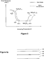
- Figure 2 shows a graph relating the sheet resistance of the three phases of nickel silicide compounds with their formation temperatures.
- nickel monosilicide is best formed between 300 - 600 degrees C, and when formed in that temperature range it provides a sheet resistance of less than three ohms per square.
- the metal-rich di-nickel silicide and the silicon-rich nickel disilicide are formed at temperatures outside of this range, and each produces a significant increase in sheet resistance.
- the high process temperatures typically used in semiconductor processing for purposes such as source/drain implant anneals can promote the conversion of nickel monosilicide into nickel disilicide, and thereby increase the sheet resistance of the silicide. Therefore a design that uses nickel monosilicide is restricted in the thermal budget that is available for further processing.
- US 6406973 relates to manufacturing of a salicide MOSFET employing silicon germanium and titanium.
- the gate of a MOSFET is capped with a layer of polycrystalline polycrystalline silicon germanium.
- Silicidation with nickel is then performed to form a nickel-germanosilicide that preferably comprises the monosilicide phase of nickel silicides.
- the source and drain regions may also employ nickel germanosilicide.
- the incorporation of germanium in the silicide provides a wider temperature range within which the monosilicide may be formed, while essentially preserving the sheet resistance exhibited by nickel monosilicide.
- the nickel germanosilicide is capable of withstanding greater temperatures during subsequent processing than nickel monosilicide, yet provides approximately the same sheet resistance and other beneficial properties as nickel monosilicide.
- a process for forming a metal oxide semiconductor field effect transistor comprising: providing a semiconductor substrate having formed thereon a gate insulating layer, a polysilicon layer formed on the gate insulating layer, and a polycrystalline silicon germanium layer formed on the polysilicon layer, the substrate comprising an epitaxial layer of strained silicon overlying a layer of silicon germanium; patterning the gate insulating layer, the polycrystalline silicon germanium layer and the polysilicon layer to form a gate, the gate comprising a gate insulator, a lower polysilicon portion and an upper polycrystalline silicon germanium portion; etching the epitaxial strained silicon layer from the source and drain regions of the MOSFET to form a strained silicon channel region of the MOSFET; replacing the etched strained silicon with silicon germanium; forming a spacer around the gate; implanting deep source and drain regions; forming a layer of nickel in contact with the upper polycrystalline silicon germanium portion of the gate and in contact with the silicon
- a metal oxide semiconductor field effect transistor (MOSFET) device comprising: a semiconductor substrate comprising a layer of silicon germanium; source and drain regions formed in the silicon germanium layer, a strained silicon channel region formed on the silicon germanium layer, the strained silicon channel regions comprising an epitaxial layer of strained silicon extending between the source and drain regions; a gate insulator overlying the channel region; a polycide gate overlying the gate insulator, the polycide gate comprising a lower polysilicon portion and an upper polycrystalline silicon germanium portion, and a nickel germanosilicide formed on the upper polycrystalline silicon germanium portion of the gate; and nickel germanosilicide contacts formed at the surfaces of the silicon germanium source and drain regions.
- MOSFET metal oxide semiconductor field effect transistor
- Figure 3 shows a graph relating the sheet resistances of nickel silicides and nickel germanosilicides to their formation temperatures.
- the graph of Figure 3 assumes a germanium/silicon composition Si 1x Ge x , where x is .1 - .4.
- the contours of the graph are similar for nickel silicides and nickel germanosilicides, varying between three to ten ohms per square, however the formation temperature range for the silicon-rich phase of nickel germanosilicide is higher than that of the silicon-rich phase of nickel silicide.
- the ideal range for formation of the monosilicide phase of nickel germanosilicide lies in the range of approximately 300 degrees C to 700 degrees C. As a result, this enables the nickel germanosilicide to withstand higher processing temperatures without significant degradation of the monosilicide phase.
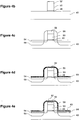
- a first preferred embodiment employs a nickel germanosilicide as a gate contact layer of a MOSFET. Structures formed during fabrication of such a device are illustrated in Figures 4a - 4f .
- Figure 4a shows a structure from which the MOSFET of the first preferred embodiment is formed.
- the structure includes a silicon semiconductor substrate 40 on which is formed a gate insulating layer 42 such as silicon oxide, a polysilicon gate conducting layer 44, and a polycrystalline silicon germanium layer 46.
- the polycrystalline silicon germanium layer 46 preferably has a composition Si 1-x Ge x , where x is typically in the range of .1 to .3, and is preferably approximately .2
- the polysilicon gate conducting layer 44 is preferably 500 - 1000 Angstroms thick
- the silicon germanium layer 46 is preferably 300 - 600 Angstroms thick.
- the polycrystalline silicon germanium layer may be formed by chemical vapor deposition using Si 2 H 6 (disilane) and GeH 4 (germane) as source gasses at a temperature of 600 - 900 degrees C, with a disilane partial pressure of 30 mPa, and a germane partial pressure of 60 mPa. Growth of the polycrystalline silicon germanium material may be initiated using these rations, or alternatively the partial pressure of germane may be gradually increased beginning from a lower pressure or zero pressure to form a gradient composition.
- the polysilicon 44 and polycrystalline silicon germanium 46 layers may be formed in distinct processing steps, however it is preferable to form the layers in situ in a continuous process in which the portion of germanium source gas is gradually introduced so as to form a graded layer. It is noted that polycrystalline silicon germanium can be deposited at lower temperatures than are required for the deposition of polysilicon, and so temperature control may be implemented along with source gas control when forming a graded structure.
- Figure 4b shows the structure of Figure 4a after patterning of the gate insulating layer, gate conducting layer and polycrystalline silicon germanium layer to form a self-aligned gate stack including an oxide gate insulator 48 and a gate comprising a lower polysilicon portion 50 and an upper polycrystalline silicon germanium portion 52.
- Figure 4c shows the structure of Figure 4b after source and drain implantation and formation of gate spacers.
- low energy dopant implantation is performed on the structure of Figure 4b to form shallow source and drain extensions 54.
- Gate spacers 56 are then formed by depositing a conformal layer of a protective material such as silicon oxide, followed by anisotropic etching to remove deposited material from the top of the gate and from the substrate surface.
- high energy dopant implantation is performed to form deep source and drain regions 58.
- the gate spacers 56 serve as an implant mask that protects the underlying shallow source and drain extensions.
- Figure 4d shows the structure of Figure 4c after formation of a conformal layer of nickel 60 over the substrate and gate stack, including the exposed surfaces of the source and drain regions 58 and the exposed surface of the gate stack.
- the nickel layer is preferable formed by physical vapor deposition (sputtering), but other well-known methods of metal layer formation may also be utilized.
- Figure 4e shows the structure of Figure 4d after performing thermal processing on the structure of Figure 4d to promote formation of silicides between the nickel layer 60 and the silicon of the source and drain regions and the polycrystalline silicon germanium of the upper portion 52 of the gate.
- Thermal processing is preferably performed using a temperature range of 350 - 700 degrees C so as to form nickel germanosilicide containing primarily the monosilicide phase. Because the silicide formation process consumes silicon, the thickness of the nickel germanosilicide layer is determined by the amount of time that thermal is performed.
- the resulting structure includes a nickel germanosilicide region 62 formed on the upper polycrystalline silicon germanium portion 52 of the gate, and nickel silicide regions 64 formed at the surfaces of the source and drain regions 56.
- processing described with respect to Figures 4a - 4f represents a preferred manner of fabricating one type of MOSFET including a nickel germanosilicide gate
- other manners of processing may be employed to realize the same structure or other MOSFET structures having a nickel germanosilicide gate.
- the preferred embodiment employs the technique of deposition of a layer of nickel followed by thermal processing
- alternative methods may be employed to form a layer of nickel germanosilicide, such as simultaneous evaporation of nickel, silicon and germanium, or co-sputtering of nickel, silicon and germanium, or sputtering from a nickel silicon germanium target.
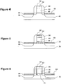
- FIG. 5 A structure in accordance with a second preferred embodiment of the invention is illustrated in Figure 5 .
- the structure of Figure 5 differs from that of Figure 4f in that the substrate includes a layer of silicon germanium 70 on which is formed a thin layer of "strained" silicon 72.
- Strained silicon is a form of silicon in which a tensile strain is applied to the silicon lattice as a result of the difference in the dimensionalities of the silicon lattice and the lattice of the underlying material on which it is formed.
- the silicon germanium lattice is more widely spaced than a pure silicon lattice, with the spacing becoming wider as the percentage of germanium increases.
- the silicon lattice aligns with the larger silicon germanium lattice during formation, a tensile strain is imparted to the silicon layer.
- the silicon atoms are pulled apart from one another.
- Relaxed silicon has a conductive band that contains six equal valence bands.
- the application of tensile strain to the silicon causes four of the six valence bands to increase in energy and two of the valence bands to decrease in energy.
- electrons effectively weigh 30 percent less when passing through the lower energy bands.
- the lower energy bands offer less resistance to electron flow.
- electrons meet with less vibrational energy from the nucleus of the silicon atom, which causes them to scatter at a rate of 500 to 1000 times less than in relaxed silicon.
- carrier mobility is dramatically increased in strained silicon compared to relaxed silicon, providing a potential increase in mobility of 80% or more for electrons and 20% or more for holes.
- the increase in mobility has been found to persist for current fields up to 1.5 megavolts/centimeter.
- the structure of Figure 5 exploits the beneficial features of strained silicon by utilizing an epitaxial layer of strained silicon 72 supported by a silicon germanium layer 70.
- the source and drain regions 58 and the channel region are formed in the strained silicon 72. Therefore, the structure of Figure 5 is formed in a manner similar to that shown in Figures 4a - 4f , with the distinction that the initial layered structure shown in Figure 4a is altered so as to have a silicon germanium layer and a strained silicon layer between the semiconductor substrate 40 and the gate insulating layer 42.
- the silicon germanium layer 70 preferably has a composition Si 1-x Ge x , where x is approximately .2, and is more generally in the range of .1 to .3.
- Silicon germanium may be grown on a silicon wafer substrate, for example, by chemical vapor deposition using Si 2 H 6 (disilane) and GeH 4 (germane) as source gases, with a substrate temperature of 600 to 900 degrees C, a Si 2 H 6 partial pressure of 30 mPa, and a GeH 4 partial pressure of 60 mPa. Growth of the silicon germanium material may be initiated using these ratios, or alternatively the partial pressure of GeH 4 may be gradually increased beginning from a lower pressure or zero pressure to form a gradient composition.
- the strained silicon layer may then be grown on the silicon germanium layer, for example by chemical vapor deposition (CVD) using Si 2 H 6 as a source gas with a partial pressure of 30mPa and a substrate temperature of approximately 600 - 900 degrees C.
- CVD chemical vapor deposition
- Figure 6 shows a structure in accordance with a third preferred embodiment.
- the structure of Figure 6 is similar to that of Figure 5 in that it employs strained silicon formed over a silicon germanium lattice.
- the strained silicon of the structure of Figure 6 is limited to a channel region 74 under the gate insulator 48 and spacer 56.
- Such a structure may be formed by etching an epitaxial strained silicon layer, and replacing the etched strained silicon with silicon germanium prior to formation of the spacer 56 and implantation of the deep source and drain regions 58.
- the strained silicon channel region 74 may be formed in an inlaid manner prior to formation of the gate insulating layer and overlying layers.
- An advantage of structures having silicon germanium source and drain regions such as the structure of Figure 6 is that the advantages of strained silicon are incorporated into the device while also incorporating the benefits of nickel germanosilicide in the source and drain regions.
- such an embodiment may be particularly desirable for providing precise control of source and drain geometry in PMOS implementations because of the reduced diffusion of boron (B) dopant in silicon germanium.
- Figure 7 shows a structure in accordance with a fourth preferred embodiment of the invention.
- the structure of Figure 7 is a silicon on insulator (SOI) structure typically referred to as a vertical double gate MOSFET or FinFET.
- SOI silicon on insulator
- the structure comprises a monolithic semiconductor body 76 formed on an insulating substrate 78.
- the semiconductor body includes source and drain regions 80 and a channel region 82 extending between the source and drain regions.
- a gate 84 is formed over and around the channel region 82 and is separated from the channel region by a gate insulator (not shown) and protected from the source and drain regions by dielectric spacers (not shown).
- the gate includes a lower polysilicon portion 86 and an upper polycrystalline silicon germanium portion 88 on which is formed a nickel germanosilicide 90.
- Nickel silicides 92 may also be formed on the source and drain regions.
- the semiconductor body 76 is formed of silicon.
- the semiconductor body 76 may be formed of silicon germanium and capped with a layer of strained silicon.
- the semiconductor body 76 may be formed of silicon germanium and capped with a layer of strained silicon in only the channel region, thus enabling the formation of nickel germanosilicide on the source and drain regions 80.
- nickel germanosilicides have equal application to other types of MOSFET structures.
- other constructions such as inverted or bottom gate MOSFETS, in which the gate underlies the channel region, may also utilize nickel germanosilicide for providing low contact resistance to source and drain regions and to gates.
- Such alternative constructions may incorporate strained silicon in the channel regions and in the source and drain regions.
- the nickel germanosilicide is comprised as much as possible by the nickel monosilicide phase.
- embodiments within the scope of the invention include a variety of MOSFET structures, each of which is characterized by the use of nickel germanosilicide as a silicide on a gate and in a source or drain region.
- Figure 8 shows a process flow for manufacture of a MOSFET encompassing the aforementioned preferred embodiments and alternatives as well as additional alternative embodiments not expressly described herein.
- a semiconductor substrate is provided (100).
- the substrate has formed thereon a gate insulating layer, a polysilicon layer formed on the gate insulating layer, and a polycrystalline silicon germanium layer formed on the polysilicon layer.
- the polycrystalline silicon germanium layer, the polysilicon layer and the gate insulating layer are then patterned to form a gate insulator and a gate overlying the gate insulator (102).
- the gate thus includes a lower polysilicon portion and an upper polycrystalline silicon germanium portion.
- a layer of nickel is formed over at least the upper polycrystalline silicon germanium portion of the gate (104).
- the substrate referred to herein may comprise a semiconductor substrate, as used in the embodiments of Figures 4f, 5 and 6 , or an insulating substrate having a semiconductor body previously patterned thereon, as used in the embodiment of Figure 8 .
- the nickel layer may be desirable to perform additional types of processing or to form different types of structures.
- the nickel layer may be preferable to alloy the nickel layer with another metal such as vanadium (Va), tantalum (Ta) or tungsten (W) to improve the phase stability of the germanosilicide.
- the additional metal may be implanted into the nickel layer or may be formed as a separate CVD or PVD layer over the nickel layer prior to germanosilicide formation.
- a polycrystalline silicon germanium gate may be employed.
- the polycrystalline silicon germanium portion of the gate may be formed by annealing a polysilicon gate in a germanium atmosphere or by implanting germanium into a polysilicon gate.
Landscapes
- Engineering & Computer Science (AREA)
- Manufacturing & Machinery (AREA)
- Physics & Mathematics (AREA)
- Chemical Kinetics & Catalysis (AREA)
- Condensed Matter Physics & Semiconductors (AREA)
- General Physics & Mathematics (AREA)
- Chemical & Material Sciences (AREA)
- Computer Hardware Design (AREA)
- Microelectronics & Electronic Packaging (AREA)
- Power Engineering (AREA)
- Electrodes Of Semiconductors (AREA)
- Insulated Gate Type Field-Effect Transistor (AREA)
- Thin Film Transistor (AREA)
Applications Claiming Priority (5)
| Application Number | Priority Date | Filing Date | Title |
|---|---|---|---|
| US41517902P | 2002-09-30 | 2002-09-30 | |
| US415179P | 2002-09-30 | ||
| US335492 | 2002-12-31 | ||
| US10/335,492 US6787864B2 (en) | 2002-09-30 | 2002-12-31 | Mosfets incorporating nickel germanosilicided gate and methods for their formation |
| PCT/US2003/028680 WO2004038807A1 (en) | 2002-09-30 | 2003-09-12 | Mosfets incorporating nickel germanosilicided gate and methods of their formation |
Publications (2)
| Publication Number | Publication Date |
|---|---|
| EP1550164A1 EP1550164A1 (en) | 2005-07-06 |
| EP1550164B1 true EP1550164B1 (en) | 2012-04-18 |
Family
ID=32033324
Family Applications (1)
| Application Number | Title | Priority Date | Filing Date |
|---|---|---|---|
| EP03752303A Expired - Lifetime EP1550164B1 (en) | 2002-09-30 | 2003-09-12 | Mosfets incorporating nickel germanosilicided gate and methods of their formation |
Country Status (8)
| Country | Link |
|---|---|
| US (1) | US6787864B2 (enExample) |
| EP (1) | EP1550164B1 (enExample) |
| JP (1) | JP4662772B2 (enExample) |
| KR (1) | KR101054057B1 (enExample) |
| CN (1) | CN100557817C (enExample) |
| AU (1) | AU2003270598A1 (enExample) |
| TW (1) | TWI338367B (enExample) |
| WO (1) | WO2004038807A1 (enExample) |
Families Citing this family (94)
| Publication number | Priority date | Publication date | Assignee | Title |
|---|---|---|---|---|
| US6703688B1 (en) * | 2001-03-02 | 2004-03-09 | Amberwave Systems Corporation | Relaxed silicon germanium platform for high speed CMOS electronics and high speed analog circuits |
| US6830976B2 (en) * | 2001-03-02 | 2004-12-14 | Amberwave Systems Corproation | Relaxed silicon germanium platform for high speed CMOS electronics and high speed analog circuits |
| US7074623B2 (en) | 2002-06-07 | 2006-07-11 | Amberwave Systems Corporation | Methods of forming strained-semiconductor-on-insulator finFET device structures |
| US6995430B2 (en) | 2002-06-07 | 2006-02-07 | Amberwave Systems Corporation | Strained-semiconductor-on-insulator device structures |
| US6946371B2 (en) | 2002-06-10 | 2005-09-20 | Amberwave Systems Corporation | Methods of fabricating semiconductor structures having epitaxially grown source and drain elements |
| US6982474B2 (en) | 2002-06-25 | 2006-01-03 | Amberwave Systems Corporation | Reacted conductive gate electrodes |
| JP3597831B2 (ja) * | 2002-07-01 | 2004-12-08 | 株式会社東芝 | 電界効果トランジスタ及びその製造方法 |
| US6746967B2 (en) * | 2002-09-30 | 2004-06-08 | Intel Corporation | Etching metal using sonication |
| US6867428B1 (en) * | 2002-10-29 | 2005-03-15 | Advanced Micro Devices, Inc. | Strained silicon NMOS having silicon source/drain extensions and method for its fabrication |
| JP4275395B2 (ja) * | 2002-12-11 | 2009-06-10 | 株式会社ルネサステクノロジ | 半導体装置の製造方法 |
| US7304336B2 (en) | 2003-02-13 | 2007-12-04 | Massachusetts Institute Of Technology | FinFET structure and method to make the same |
| JP4585510B2 (ja) | 2003-03-07 | 2010-11-24 | 台湾積體電路製造股▲ふん▼有限公司 | シャロートレンチアイソレーションプロセス |
| TWI231994B (en) * | 2003-04-04 | 2005-05-01 | Univ Nat Taiwan | Strained Si FinFET |
| US6905976B2 (en) * | 2003-05-06 | 2005-06-14 | International Business Machines Corporation | Structure and method of forming a notched gate field effect transistor |
| US7192876B2 (en) * | 2003-05-22 | 2007-03-20 | Freescale Semiconductor, Inc. | Transistor with independent gate structures |
| JP4008860B2 (ja) * | 2003-07-11 | 2007-11-14 | 株式会社東芝 | 半導体装置の製造方法 |
| US6921982B2 (en) * | 2003-07-21 | 2005-07-26 | International Business Machines Corporation | FET channel having a strained lattice structure along multiple surfaces |
| KR100487566B1 (ko) * | 2003-07-23 | 2005-05-03 | 삼성전자주식회사 | 핀 전계 효과 트랜지스터 및 그 형성 방법 |
| JP2005086024A (ja) * | 2003-09-09 | 2005-03-31 | Toshiba Corp | 半導体装置及びその製造方法 |
| US7175966B2 (en) * | 2003-09-19 | 2007-02-13 | International Business Machines Corporation | Water and aqueous base soluble antireflective coating/hardmask materials |
| US20050090082A1 (en) * | 2003-10-28 | 2005-04-28 | Texas Instruments Incorporated | Method and system for improving performance of MOSFETs |
| KR100738066B1 (ko) * | 2003-12-01 | 2007-07-12 | 삼성전자주식회사 | 열적 안정성이 우수한 실리사이드막 형성방법, 이방법으로 형성된 실리사이드막이 구비된 반도체 소자와반도체 메모리 소자 및 이들 소자의 제조 방법 |
| US6949482B2 (en) * | 2003-12-08 | 2005-09-27 | Intel Corporation | Method for improving transistor performance through reducing the salicide interface resistance |
| JP3879003B2 (ja) * | 2004-02-26 | 2007-02-07 | 国立大学法人名古屋大学 | シリサイド膜の作製方法 |
| US7235471B2 (en) * | 2004-05-26 | 2007-06-26 | Freescale Semiconductor, Inc. | Method for forming a semiconductor device having a silicide layer |
| US7009226B1 (en) * | 2004-07-12 | 2006-03-07 | Advanced Micro Devices, Inc. | In-situ nitride/oxynitride processing with reduced deposition surface pattern sensitivity |
| JP2008508713A (ja) * | 2004-07-27 | 2008-03-21 | エージェンシー フォー サイエンス,テクノロジー アンド リサーチ | 高信頼性コンタクト |
| US7435672B2 (en) * | 2004-07-30 | 2008-10-14 | Texas Instruments Incorporated | Metal-germanium physical vapor deposition for semiconductor device defect reduction |
| US7288448B2 (en) * | 2004-08-24 | 2007-10-30 | Orlowski Marius K | Method and apparatus for mobility enhancement in a semiconductor device |
| US7166897B2 (en) * | 2004-08-24 | 2007-01-23 | Freescale Semiconductor, Inc. | Method and apparatus for performance enhancement in an asymmetrical semiconductor device |
| US7348641B2 (en) * | 2004-08-31 | 2008-03-25 | International Business Machines Corporation | Structure and method of making double-gated self-aligned finFET having gates of different lengths |
| US7241649B2 (en) * | 2004-10-29 | 2007-07-10 | International Business Machines Corporation | FinFET body contact structure |
| US7393733B2 (en) | 2004-12-01 | 2008-07-01 | Amberwave Systems Corporation | Methods of forming hybrid fin field-effect transistor structures |
| KR100678314B1 (ko) | 2004-12-15 | 2007-02-02 | 동부일렉트로닉스 주식회사 | 저접촉저항을 갖는 반도체 소자의 제조방법 |
| JP4969779B2 (ja) * | 2004-12-28 | 2012-07-04 | 株式会社東芝 | 半導体装置の製造方法 |
| CN100487879C (zh) * | 2004-12-28 | 2009-05-13 | 松下电器产业株式会社 | 半导体纳米导线及其制法和包括该纳米导线的半导体装置 |
| US20060163670A1 (en) * | 2005-01-27 | 2006-07-27 | International Business Machines Corporation | Dual silicide process to improve device performance |
| US7319063B2 (en) * | 2005-02-02 | 2008-01-15 | United Microelectronics Corp. | Fin field effect transistor and method for manufacturing fin field effect transistor |
| US7348232B2 (en) * | 2005-03-01 | 2008-03-25 | Texas Instruments Incorporated | Highly activated carbon selective epitaxial process for CMOS |
| US8324660B2 (en) | 2005-05-17 | 2012-12-04 | Taiwan Semiconductor Manufacturing Company, Ltd. | Lattice-mismatched semiconductor structures with reduced dislocation defect densities and related methods for device fabrication |
| US9153645B2 (en) | 2005-05-17 | 2015-10-06 | Taiwan Semiconductor Manufacturing Company, Ltd. | Lattice-mismatched semiconductor structures with reduced dislocation defect densities and related methods for device fabrication |
| US7902598B2 (en) | 2005-06-24 | 2011-03-08 | Micron Technology, Inc. | Two-sided surround access transistor for a 4.5F2 DRAM cell |
| US7109116B1 (en) * | 2005-07-21 | 2006-09-19 | International Business Machines Corporation | Method for reducing dendrite formation in nickel silicon salicide processes |
| KR100685898B1 (ko) | 2005-07-27 | 2007-02-26 | 동부일렉트로닉스 주식회사 | 반도체 소자의 제조방법 |
| US7696567B2 (en) | 2005-08-31 | 2010-04-13 | Micron Technology, Inc | Semiconductor memory device |
| US7566609B2 (en) * | 2005-11-29 | 2009-07-28 | International Business Machines Corporation | Method of manufacturing a semiconductor structure |
| US7459382B2 (en) | 2006-03-24 | 2008-12-02 | International Business Machines Corporation | Field effect device with reduced thickness gate |
| US7777250B2 (en) | 2006-03-24 | 2010-08-17 | Taiwan Semiconductor Manufacturing Company, Ltd. | Lattice-mismatched semiconductor structures and related methods for device fabrication |
| US20070238236A1 (en) * | 2006-03-28 | 2007-10-11 | Cook Ted Jr | Structure and fabrication method of a selectively deposited capping layer on an epitaxially grown source drain |
| US7618891B2 (en) * | 2006-05-01 | 2009-11-17 | International Business Machines Corporation | Method for forming self-aligned metal silicide contacts |
| US8173551B2 (en) | 2006-09-07 | 2012-05-08 | Taiwan Semiconductor Manufacturing Co., Ltd. | Defect reduction using aspect ratio trapping |
| KR100798814B1 (ko) * | 2006-09-20 | 2008-01-28 | 삼성전자주식회사 | 전계 효과 트랜지스터를 포함하는 반도체 소자 및 그 형성방법 |
| US7799592B2 (en) | 2006-09-27 | 2010-09-21 | Taiwan Semiconductor Manufacturing Company, Ltd. | Tri-gate field-effect transistors formed by aspect ratio trapping |
| US7875958B2 (en) | 2006-09-27 | 2011-01-25 | Taiwan Semiconductor Manufacturing Company, Ltd. | Quantum tunneling devices and circuits with lattice-mismatched semiconductor structures |
| US20080187018A1 (en) | 2006-10-19 | 2008-08-07 | Amberwave Systems Corporation | Distributed feedback lasers formed via aspect ratio trapping |
| US7550796B2 (en) * | 2006-12-06 | 2009-06-23 | Electronics And Telecommunications Research Institute | Germanium semiconductor device and method of manufacturing the same |
| KR20080062764A (ko) * | 2006-12-29 | 2008-07-03 | 삼성전자주식회사 | 게르마늄실리사이드 형성방법 및 이를 적용하여 게르마늄실리사이드가 형성된 디바이스 |
| US8237151B2 (en) | 2009-01-09 | 2012-08-07 | Taiwan Semiconductor Manufacturing Company, Ltd. | Diode-based devices and methods for making the same |
| US8304805B2 (en) | 2009-01-09 | 2012-11-06 | Taiwan Semiconductor Manufacturing Company, Ltd. | Semiconductor diodes fabricated by aspect ratio trapping with coalesced films |
| US9508890B2 (en) | 2007-04-09 | 2016-11-29 | Taiwan Semiconductor Manufacturing Company, Ltd. | Photovoltaics on silicon |
| US7825328B2 (en) | 2007-04-09 | 2010-11-02 | Taiwan Semiconductor Manufacturing Company, Ltd. | Nitride-based multi-junction solar cell modules and methods for making the same |
| KR100861211B1 (ko) * | 2007-04-12 | 2008-09-30 | 주식회사 하이닉스반도체 | 반도체 소자 및 그 제조 방법 |
| US8329541B2 (en) | 2007-06-15 | 2012-12-11 | Taiwan Semiconductor Manufacturing Company, Ltd. | InP-based transistor fabrication |
| DE112008002387B4 (de) | 2007-09-07 | 2022-04-07 | Taiwan Semiconductor Manufacturing Co., Ltd. | Struktur einer Mehrfachübergangs-Solarzelle, Verfahren zur Bildung einer photonischenVorrichtung, Photovoltaische Mehrfachübergangs-Zelle und Photovoltaische Mehrfachübergangs-Zellenvorrichtung, |
| US20090065804A1 (en) | 2007-09-10 | 2009-03-12 | International Business Machines Corporation | Bipolar transistor with low resistance base contact and method of making the same |
| JP5525127B2 (ja) * | 2007-11-12 | 2014-06-18 | ピーエスフォー ルクスコ エスエイアールエル | 半導体装置及びその製造方法 |
| KR101194843B1 (ko) | 2007-12-07 | 2012-10-25 | 삼성전자주식회사 | Ge 실리사이드층의 형성방법, Ge 실리사이드층을포함하는 반도체 소자 및 그의 제조방법 |
| US20090152590A1 (en) * | 2007-12-13 | 2009-06-18 | International Business Machines Corporation | Method and structure for semiconductor devices with silicon-germanium deposits |
| US8183667B2 (en) | 2008-06-03 | 2012-05-22 | Taiwan Semiconductor Manufacturing Co., Ltd. | Epitaxial growth of crystalline material |
| US8274097B2 (en) | 2008-07-01 | 2012-09-25 | Taiwan Semiconductor Manufacturing Company, Ltd. | Reduction of edge effects from aspect ratio trapping |
| US8981427B2 (en) | 2008-07-15 | 2015-03-17 | Taiwan Semiconductor Manufacturing Company, Ltd. | Polishing of small composite semiconductor materials |
| US20100072515A1 (en) | 2008-09-19 | 2010-03-25 | Amberwave Systems Corporation | Fabrication and structures of crystalline material |
| US8034697B2 (en) | 2008-09-19 | 2011-10-11 | Taiwan Semiconductor Manufacturing Company, Ltd. | Formation of devices by epitaxial layer overgrowth |
| US8253211B2 (en) | 2008-09-24 | 2012-08-28 | Taiwan Semiconductor Manufacturing Company, Ltd. | Semiconductor sensor structures with reduced dislocation defect densities |
| DE102008053955B4 (de) * | 2008-10-31 | 2010-10-21 | Advanced Micro Devices, Inc., Sunnyvale | Verfahren zur Herstellung eines Halbleiterbauelements als Transistor mit Verbesserung der Verspannungsübertragung durch eine späte Gaterekristallisierung und Transistor |
| KR101561059B1 (ko) * | 2008-11-20 | 2015-10-16 | 삼성전자주식회사 | 반도체 소자 및 그 제조 방법 |
| US9379011B2 (en) * | 2008-12-19 | 2016-06-28 | Asm International N.V. | Methods for depositing nickel films and for making nickel silicide and nickel germanide |
| WO2010114956A1 (en) | 2009-04-02 | 2010-10-07 | Taiwan Semiconductor Manufacturing Company, Ltd. | Devices formed from a non-polar plane of a crystalline material and method of making the same |
| FR2953989B1 (fr) * | 2009-12-10 | 2012-05-18 | Commissariat Energie Atomique | Procede de formation de materiaux metalliques comportant des semi-conducteurs |
| EP2519969A4 (en) * | 2009-12-28 | 2016-07-06 | Semiconductor Energy Lab | SEMICONDUCTOR COMPONENT |
| US8729627B2 (en) * | 2010-05-14 | 2014-05-20 | Taiwan Semiconductor Manufacturing Company, Ltd. | Strained channel integrated circuit devices |
| US20120139014A1 (en) * | 2010-12-01 | 2012-06-07 | International Business Machines Corporation | Structure and method for low temperature gate stack for advanced substrates |
| KR20140097244A (ko) | 2011-11-08 | 2014-08-06 | 토소우 에스엠디, 인크 | 특별한 표면 처리를 하고 양호한 입자 성능을 가진 실리콘 스퍼터링 타겟 및 그 제조 방법들 |
| US8580686B1 (en) * | 2012-04-23 | 2013-11-12 | Globalfoundries Inc. | Silicidation and/or germanidation on SiGe or Ge by cosputtering Ni and Ge and using an intralayer for thermal stability |
| US8624324B1 (en) * | 2012-08-10 | 2014-01-07 | Taiwan Semiconductor Manufacturing Company, Ltd. | Connecting through vias to devices |
| US9377394B2 (en) | 2012-10-16 | 2016-06-28 | Seagate Technology Llc | Distinguishing foreign surface features from native surface features |
| CN104425364B (zh) * | 2013-09-09 | 2017-09-29 | 中芯国际集成电路制造(上海)有限公司 | 连接线的形成方法 |
| US10032876B2 (en) * | 2014-03-13 | 2018-07-24 | Taiwan Semiconductor Manufacturing Company, Ltd. | Contact silicide having a non-angular profile |
| US9590105B2 (en) * | 2014-04-07 | 2017-03-07 | National Chiao-Tung University | Semiconductor device with metal alloy over fin, conductive layer over channel region of fin, and semiconductive layer over conductive layer and formation thereof |
| KR20160058499A (ko) | 2014-11-17 | 2016-05-25 | 삼성전자주식회사 | 반도체 소자, 및 그 반도체 소자의 제조방법과 제조장치 |
| US9865466B2 (en) * | 2015-09-25 | 2018-01-09 | Applied Materials, Inc. | Silicide phase control by confinement |
| CN109950151B (zh) * | 2017-12-20 | 2022-02-15 | 中芯国际集成电路制造(上海)有限公司 | Pmos晶体管及其形成方法 |
| US12476144B2 (en) * | 2021-12-07 | 2025-11-18 | International Business Machines Corporation | Etch back and film profile shaping of selective dielectric deposition |
| CN116632062A (zh) * | 2022-02-14 | 2023-08-22 | 联华电子股份有限公司 | 中压晶体管及其制作方法 |
Family Cites Families (13)
| Publication number | Priority date | Publication date | Assignee | Title |
|---|---|---|---|---|
| JPH05183160A (ja) * | 1991-12-26 | 1993-07-23 | Toshiba Corp | 半導体装置及びその製造方法 |
| JPH07202178A (ja) * | 1993-12-28 | 1995-08-04 | Toshiba Corp | 半導体装置およびその製造方法 |
| US5561302A (en) * | 1994-09-26 | 1996-10-01 | Motorola, Inc. | Enhanced mobility MOSFET device and method |
| JP3326427B2 (ja) * | 1996-09-17 | 2002-09-24 | 松下電器産業株式会社 | 半導体装置及びその製造方法 |
| JP4092766B2 (ja) * | 1998-03-27 | 2008-05-28 | 富士通株式会社 | 半導体装置 |
| JP2002530864A (ja) * | 1998-11-12 | 2002-09-17 | インテル・コーポレーション | 階段ソース/ドレイン接合部を有する電界効果トランジスタ構造 |
| KR100332108B1 (ko) * | 1999-06-29 | 2002-04-10 | 박종섭 | 반도체 소자의 트랜지스터 및 그 제조 방법 |
| JP2002110989A (ja) * | 2000-09-27 | 2002-04-12 | Japan Science & Technology Corp | 半導体集積回路装置およびその製造方法 |
| EP1364411A1 (en) * | 2001-03-02 | 2003-11-26 | Amberwave Systems Corporation | Relaxed silicon germanium platform for high speed cmos electronics and high speed analog circuits |
| US6724008B2 (en) * | 2001-03-02 | 2004-04-20 | Amberwave Systems Corporation | Relaxed silicon germanium platform for high speed CMOS electronics and high speed analog circuits |
| JP3547419B2 (ja) * | 2001-03-13 | 2004-07-28 | 株式会社東芝 | 半導体装置及びその製造方法 |
| US6506637B2 (en) * | 2001-03-23 | 2003-01-14 | Sharp Laboratories Of America, Inc. | Method to form thermally stable nickel germanosilicide on SiGe |
| US6974735B2 (en) * | 2001-08-09 | 2005-12-13 | Amberwave Systems Corporation | Dual layer Semiconductor Devices |
-
2002
- 2002-12-31 US US10/335,492 patent/US6787864B2/en not_active Expired - Lifetime
-
2003
- 2003-09-12 CN CN03823253.7A patent/CN100557817C/zh not_active Expired - Lifetime
- 2003-09-12 AU AU2003270598A patent/AU2003270598A1/en not_active Abandoned
- 2003-09-12 KR KR1020057005285A patent/KR101054057B1/ko not_active Expired - Lifetime
- 2003-09-12 WO PCT/US2003/028680 patent/WO2004038807A1/en not_active Ceased
- 2003-09-12 JP JP2004546734A patent/JP4662772B2/ja not_active Expired - Lifetime
- 2003-09-12 EP EP03752303A patent/EP1550164B1/en not_active Expired - Lifetime
- 2003-09-19 TW TW092125871A patent/TWI338367B/zh not_active IP Right Cessation
Also Published As
| Publication number | Publication date |
|---|---|
| JP2006501685A (ja) | 2006-01-12 |
| US6787864B2 (en) | 2004-09-07 |
| KR101054057B1 (ko) | 2011-08-04 |
| CN100557817C (zh) | 2009-11-04 |
| EP1550164A1 (en) | 2005-07-06 |
| AU2003270598A1 (en) | 2004-05-13 |
| US20040061191A1 (en) | 2004-04-01 |
| TW200417029A (en) | 2004-09-01 |
| JP4662772B2 (ja) | 2011-03-30 |
| WO2004038807A1 (en) | 2004-05-06 |
| CN1685520A (zh) | 2005-10-19 |
| TWI338367B (en) | 2011-03-01 |
| KR20050070011A (ko) | 2005-07-05 |
Similar Documents
| Publication | Publication Date | Title |
|---|---|---|
| EP1550164B1 (en) | Mosfets incorporating nickel germanosilicided gate and methods of their formation | |
| US6703648B1 (en) | Strained silicon PMOS having silicon germanium source/drain extensions and method for its fabrication | |
| KR100362751B1 (ko) | 반도체소자의콘택트홀및그형성방법 | |
| US8278718B2 (en) | Stressed barrier plug slot contact structure for transistor performance enhancement | |
| US6657223B1 (en) | Strained silicon MOSFET having silicon source/drain regions and method for its fabrication | |
| US6902991B2 (en) | Semiconductor device having a thick strained silicon layer and method of its formation | |
| TW535260B (en) | Method of manufacturing semiconductor device | |
| US6730576B1 (en) | Method of forming a thick strained silicon layer and semiconductor structures incorporating a thick strained silicon layer | |
| TWI387010B (zh) | 用於製造電晶體之方法 | |
| US20140374844A1 (en) | Method for forming metal semiconductor alloys in contact holes and trenches | |
| US20050054164A1 (en) | Strained silicon MOSFETs having reduced diffusion of n-type dopants | |
| US6849527B1 (en) | Strained silicon MOSFET having improved carrier mobility, strained silicon CMOS device, and methods of their formation | |
| JP2006351581A (ja) | 半導体装置の製造方法 | |
| JP5659416B2 (ja) | 半導体素子の製造方法 | |
| US6756276B1 (en) | Strained silicon MOSFET having improved source/drain extension dopant diffusion resistance and method for its fabrication | |
| US6867428B1 (en) | Strained silicon NMOS having silicon source/drain extensions and method for its fabrication | |
| US8575014B2 (en) | Semiconductor device fabricated using a metal microstructure control process | |
| US7365010B2 (en) | Semiconductor device having carbon-containing metal silicide layer and method of fabricating the same | |
| US6797614B1 (en) | Nickel alloy for SMOS process silicidation | |
| US6924182B1 (en) | Strained silicon MOSFET having reduced leakage and method of its formation | |
| KR100481185B1 (ko) | 완전 게이트 실리사이드화 공정을 사용하여 모스트랜지스터를 제조하는 방법 | |
| JP4533155B2 (ja) | 半導体装置及びその製造方法 | |
| US6893929B1 (en) | Method of forming strained silicon MOSFET having improved threshold voltage under the gate ends | |
| US20060049470A1 (en) | Double layer polysilicon gate electrode |
Legal Events
| Date | Code | Title | Description |
|---|---|---|---|
| PUAI | Public reference made under article 153(3) epc to a published international application that has entered the european phase |
Free format text: ORIGINAL CODE: 0009012 |
|
| 17P | Request for examination filed |
Effective date: 20050311 |
|
| AK | Designated contracting states |
Kind code of ref document: A1 Designated state(s): AT BE BG CH CY CZ DE DK EE ES FI FR GB GR HU IE IT LI LU MC NL PT RO SE SI SK TR |
|
| AX | Request for extension of the european patent |
Extension state: AL LT LV MK |
|
| DAX | Request for extension of the european patent (deleted) | ||
| RBV | Designated contracting states (corrected) |
Designated state(s): DE FR GB |
|
| 17Q | First examination report despatched |
Effective date: 20081128 |
|
| GRAP | Despatch of communication of intention to grant a patent |
Free format text: ORIGINAL CODE: EPIDOSNIGR1 |
|
| GRAS | Grant fee paid |
Free format text: ORIGINAL CODE: EPIDOSNIGR3 |
|
| GRAA | (expected) grant |
Free format text: ORIGINAL CODE: 0009210 |
|
| AK | Designated contracting states |
Kind code of ref document: B1 Designated state(s): DE FR GB |
|
| REG | Reference to a national code |
Ref country code: GB Ref legal event code: FG4D |
|
| REG | Reference to a national code |
Ref country code: DE Ref legal event code: R096 Ref document number: 60340658 Country of ref document: DE Effective date: 20120614 |
|
| PLBE | No opposition filed within time limit |
Free format text: ORIGINAL CODE: 0009261 |
|
| STAA | Information on the status of an ep patent application or granted ep patent |
Free format text: STATUS: NO OPPOSITION FILED WITHIN TIME LIMIT |
|
| 26N | No opposition filed |
Effective date: 20130121 |
|
| REG | Reference to a national code |
Ref country code: DE Ref legal event code: R097 Ref document number: 60340658 Country of ref document: DE Effective date: 20130121 |
|
| REG | Reference to a national code |
Ref country code: FR Ref legal event code: ST Effective date: 20130531 |
|
| PG25 | Lapsed in a contracting state [announced via postgrant information from national office to epo] |
Ref country code: FR Free format text: LAPSE BECAUSE OF NON-PAYMENT OF DUE FEES Effective date: 20121001 |
|
| PGFP | Annual fee paid to national office [announced via postgrant information from national office to epo] |
Ref country code: GB Payment date: 20220923 Year of fee payment: 20 Ref country code: DE Payment date: 20220617 Year of fee payment: 20 |
|
| P01 | Opt-out of the competence of the unified patent court (upc) registered |
Effective date: 20230530 |
|
| REG | Reference to a national code |
Ref country code: DE Ref legal event code: R071 Ref document number: 60340658 Country of ref document: DE |
|
| REG | Reference to a national code |
Ref country code: GB Ref legal event code: PE20 Expiry date: 20230911 |
|
| PG25 | Lapsed in a contracting state [announced via postgrant information from national office to epo] |
Ref country code: GB Free format text: LAPSE BECAUSE OF EXPIRATION OF PROTECTION Effective date: 20230911 |