EP1503216B1 - Sheet-form connector and production method and application therefor - Google Patents
Sheet-form connector and production method and application therefor Download PDFInfo
- Publication number
- EP1503216B1 EP1503216B1 EP03758872A EP03758872A EP1503216B1 EP 1503216 B1 EP1503216 B1 EP 1503216B1 EP 03758872 A EP03758872 A EP 03758872A EP 03758872 A EP03758872 A EP 03758872A EP 1503216 B1 EP1503216 B1 EP 1503216B1
- Authority
- EP
- European Patent Office
- Prior art keywords
- sheet
- insulating sheet
- metal layer
- connector
- front surface
- Prior art date
- Legal status (The legal status is an assumption and is not a legal conclusion. Google has not performed a legal analysis and makes no representation as to the accuracy of the status listed.)
- Expired - Lifetime
Links
- 238000004519 manufacturing process Methods 0.000 title claims abstract description 26
- 229910052751 metal Inorganic materials 0.000 claims description 224
- 239000002184 metal Substances 0.000 claims description 224
- 238000007689 inspection Methods 0.000 claims description 145
- 239000002648 laminated material Substances 0.000 claims description 91
- 238000011282 treatment Methods 0.000 claims description 88
- 238000005530 etching Methods 0.000 claims description 68
- 239000000523 sample Substances 0.000 claims description 46
- 239000000463 material Substances 0.000 claims description 41
- 238000007747 plating Methods 0.000 claims description 35
- 238000000034 method Methods 0.000 claims description 34
- 230000008569 process Effects 0.000 claims description 27
- 238000011049 filling Methods 0.000 claims description 4
- 239000011810 insulating material Substances 0.000 claims 2
- 239000010410 layer Substances 0.000 description 218
- 239000002245 particle Substances 0.000 description 90
- 235000012431 wafers Nutrition 0.000 description 66
- 239000007771 core particle Substances 0.000 description 43
- 230000005291 magnetic effect Effects 0.000 description 43
- 238000012360 testing method Methods 0.000 description 36
- PXHVJJICTQNCMI-UHFFFAOYSA-N Nickel Chemical compound [Ni] PXHVJJICTQNCMI-UHFFFAOYSA-N 0.000 description 30
- 229920002379 silicone rubber Polymers 0.000 description 29
- 239000004020 conductor Substances 0.000 description 28
- 238000010276 construction Methods 0.000 description 20
- HEMHJVSKTPXQMS-UHFFFAOYSA-M Sodium hydroxide Chemical compound [OH-].[Na+] HEMHJVSKTPXQMS-UHFFFAOYSA-M 0.000 description 18
- RYGMFSIKBFXOCR-UHFFFAOYSA-N Copper Chemical compound [Cu] RYGMFSIKBFXOCR-UHFFFAOYSA-N 0.000 description 16
- 239000004944 Liquid Silicone Rubber Substances 0.000 description 16
- 229910052802 copper Inorganic materials 0.000 description 16
- 239000010949 copper Substances 0.000 description 16
- 229920001721 polyimide Polymers 0.000 description 16
- 229910052759 nickel Inorganic materials 0.000 description 15
- 239000004642 Polyimide Substances 0.000 description 14
- 239000004945 silicone rubber Substances 0.000 description 12
- 230000015572 biosynthetic process Effects 0.000 description 11
- 230000000717 retained effect Effects 0.000 description 11
- PCHJSUWPFVWCPO-UHFFFAOYSA-N gold Chemical compound [Au] PCHJSUWPFVWCPO-UHFFFAOYSA-N 0.000 description 10
- 229910052737 gold Inorganic materials 0.000 description 10
- 239000010931 gold Substances 0.000 description 10
- 239000002002 slurry Substances 0.000 description 10
- 229910045601 alloy Inorganic materials 0.000 description 9
- 239000000956 alloy Substances 0.000 description 9
- OAKJQQAXSVQMHS-UHFFFAOYSA-N Hydrazine Chemical compound NN OAKJQQAXSVQMHS-UHFFFAOYSA-N 0.000 description 8
- XEEYBQQBJWHFJM-UHFFFAOYSA-N Iron Chemical compound [Fe] XEEYBQQBJWHFJM-UHFFFAOYSA-N 0.000 description 8
- VYPSYNLAJGMNEJ-UHFFFAOYSA-N Silicium dioxide Chemical compound O=[Si]=O VYPSYNLAJGMNEJ-UHFFFAOYSA-N 0.000 description 8
- 238000009713 electroplating Methods 0.000 description 8
- 230000002093 peripheral effect Effects 0.000 description 8
- BASFCYQUMIYNBI-UHFFFAOYSA-N platinum Chemical compound [Pt] BASFCYQUMIYNBI-UHFFFAOYSA-N 0.000 description 8
- 239000000243 solution Substances 0.000 description 8
- 239000011347 resin Substances 0.000 description 7
- 229920005989 resin Polymers 0.000 description 7
- 239000000126 substance Substances 0.000 description 7
- KDLHZDBZIXYQEI-UHFFFAOYSA-N Palladium Chemical compound [Pd] KDLHZDBZIXYQEI-UHFFFAOYSA-N 0.000 description 6
- 239000003054 catalyst Substances 0.000 description 6
- 230000000052 comparative effect Effects 0.000 description 6
- 230000006835 compression Effects 0.000 description 6
- 238000007906 compression Methods 0.000 description 6
- 238000006073 displacement reaction Methods 0.000 description 6
- 239000011521 glass Substances 0.000 description 6
- 239000000203 mixture Substances 0.000 description 6
- 239000000047 product Substances 0.000 description 6
- XLYOFNOQVPJJNP-UHFFFAOYSA-N water Substances O XLYOFNOQVPJJNP-UHFFFAOYSA-N 0.000 description 6
- 239000007864 aqueous solution Substances 0.000 description 5
- 239000011248 coating agent Substances 0.000 description 5
- 238000000576 coating method Methods 0.000 description 5
- 239000007822 coupling agent Substances 0.000 description 5
- 238000007772 electroless plating Methods 0.000 description 5
- 238000000866 electrolytic etching Methods 0.000 description 5
- 150000002739 metals Chemical class 0.000 description 5
- 239000008213 purified water Substances 0.000 description 5
- 229920006259 thermoplastic polyimide Polymers 0.000 description 5
- VEXZGXHMUGYJMC-UHFFFAOYSA-N Hydrochloric acid Chemical compound Cl VEXZGXHMUGYJMC-UHFFFAOYSA-N 0.000 description 4
- 229910021578 Iron(III) chloride Inorganic materials 0.000 description 4
- BQCADISMDOOEFD-UHFFFAOYSA-N Silver Chemical compound [Ag] BQCADISMDOOEFD-UHFFFAOYSA-N 0.000 description 4
- 238000010306 acid treatment Methods 0.000 description 4
- PNEYBMLMFCGWSK-UHFFFAOYSA-N aluminium oxide Inorganic materials [O-2].[O-2].[O-2].[Al+3].[Al+3] PNEYBMLMFCGWSK-UHFFFAOYSA-N 0.000 description 4
- 238000009826 distribution Methods 0.000 description 4
- 230000001747 exhibiting effect Effects 0.000 description 4
- 229910052742 iron Inorganic materials 0.000 description 4
- RBTARNINKXHZNM-UHFFFAOYSA-K iron trichloride Chemical compound Cl[Fe](Cl)Cl RBTARNINKXHZNM-UHFFFAOYSA-K 0.000 description 4
- 238000010030 laminating Methods 0.000 description 4
- 239000007788 liquid Substances 0.000 description 4
- QSHDDOUJBYECFT-UHFFFAOYSA-N mercury Chemical compound [Hg] QSHDDOUJBYECFT-UHFFFAOYSA-N 0.000 description 4
- 229910052753 mercury Inorganic materials 0.000 description 4
- 239000012778 molding material Substances 0.000 description 4
- 238000000206 photolithography Methods 0.000 description 4
- 229910052697 platinum Inorganic materials 0.000 description 4
- 239000004065 semiconductor Substances 0.000 description 4
- 229910052709 silver Inorganic materials 0.000 description 4
- 239000004332 silver Substances 0.000 description 4
- 238000013112 stability test Methods 0.000 description 4
- 239000006228 supernatant Substances 0.000 description 4
- 238000005406 washing Methods 0.000 description 4
- 239000011247 coating layer Substances 0.000 description 3
- 229910017052 cobalt Inorganic materials 0.000 description 3
- 239000010941 cobalt Substances 0.000 description 3
- GUTLYIVDDKVIGB-UHFFFAOYSA-N cobalt atom Chemical compound [Co] GUTLYIVDDKVIGB-UHFFFAOYSA-N 0.000 description 3
- 230000000694 effects Effects 0.000 description 3
- 230000005415 magnetization Effects 0.000 description 3
- 239000007769 metal material Substances 0.000 description 3
- 229910052763 palladium Inorganic materials 0.000 description 3
- 229920001296 polysiloxane Polymers 0.000 description 3
- -1 polysiloxane Polymers 0.000 description 3
- 238000002360 preparation method Methods 0.000 description 3
- 239000000377 silicon dioxide Substances 0.000 description 3
- 125000000391 vinyl group Chemical group [H]C([*])=C([H])[H] 0.000 description 3
- QGZKDVFQNNGYKY-UHFFFAOYSA-N Ammonia Chemical compound N QGZKDVFQNNGYKY-UHFFFAOYSA-N 0.000 description 2
- LTPBRCUWZOMYOC-UHFFFAOYSA-N Beryllium oxide Chemical compound O=[Be] LTPBRCUWZOMYOC-UHFFFAOYSA-N 0.000 description 2
- VYZAMTAEIAYCRO-UHFFFAOYSA-N Chromium Chemical compound [Cr] VYZAMTAEIAYCRO-UHFFFAOYSA-N 0.000 description 2
- 229910000942 Elinvar Inorganic materials 0.000 description 2
- 229910001374 Invar Inorganic materials 0.000 description 2
- 229920000106 Liquid crystal polymer Polymers 0.000 description 2
- 239000004977 Liquid-crystal polymers (LCPs) Substances 0.000 description 2
- XYFCBTPGUUZFHI-UHFFFAOYSA-N Phosphine Chemical compound P XYFCBTPGUUZFHI-UHFFFAOYSA-N 0.000 description 2
- 229910000831 Steel Inorganic materials 0.000 description 2
- 239000002253 acid Substances 0.000 description 2
- 229910010293 ceramic material Inorganic materials 0.000 description 2
- 229910052804 chromium Inorganic materials 0.000 description 2
- 239000011651 chromium Substances 0.000 description 2
- 239000006185 dispersion Substances 0.000 description 2
- 229920001971 elastomer Polymers 0.000 description 2
- 239000000806 elastomer Substances 0.000 description 2
- 230000005484 gravity Effects 0.000 description 2
- 230000005389 magnetism Effects 0.000 description 2
- 238000012986 modification Methods 0.000 description 2
- 230000004048 modification Effects 0.000 description 2
- 229920002120 photoresistant polymer Polymers 0.000 description 2
- 239000009719 polyimide resin Substances 0.000 description 2
- 239000000843 powder Substances 0.000 description 2
- 230000009467 reduction Effects 0.000 description 2
- 239000011369 resultant mixture Substances 0.000 description 2
- 239000010959 steel Substances 0.000 description 2
- 238000003756 stirring Methods 0.000 description 2
- JYEUMXHLPRZUAT-UHFFFAOYSA-N 1,2,3-triazine Chemical compound C1=CN=NN=C1 JYEUMXHLPRZUAT-UHFFFAOYSA-N 0.000 description 1
- XQUPVDVFXZDTLT-UHFFFAOYSA-N 1-[4-[[4-(2,5-dioxopyrrol-1-yl)phenyl]methyl]phenyl]pyrrole-2,5-dione Chemical compound O=C1C=CC(=O)N1C(C=C1)=CC=C1CC1=CC=C(N2C(C=CC2=O)=O)C=C1 XQUPVDVFXZDTLT-UHFFFAOYSA-N 0.000 description 1
- RZVAJINKPMORJF-UHFFFAOYSA-N Acetaminophen Chemical compound CC(=O)NC1=CC=C(O)C=C1 RZVAJINKPMORJF-UHFFFAOYSA-N 0.000 description 1
- 229910052582 BN Inorganic materials 0.000 description 1
- PZNSFCLAULLKQX-UHFFFAOYSA-N Boron nitride Chemical compound N#B PZNSFCLAULLKQX-UHFFFAOYSA-N 0.000 description 1
- VEXZGXHMUGYJMC-UHFFFAOYSA-M Chloride anion Chemical compound [Cl-] VEXZGXHMUGYJMC-UHFFFAOYSA-M 0.000 description 1
- FYYHWMGAXLPEAU-UHFFFAOYSA-N Magnesium Chemical compound [Mg] FYYHWMGAXLPEAU-UHFFFAOYSA-N 0.000 description 1
- ZOKXTWBITQBERF-UHFFFAOYSA-N Molybdenum Chemical compound [Mo] ZOKXTWBITQBERF-UHFFFAOYSA-N 0.000 description 1
- 239000006087 Silane Coupling Agent Substances 0.000 description 1
- XUIMIQQOPSSXEZ-UHFFFAOYSA-N Silicon Chemical compound [Si] XUIMIQQOPSSXEZ-UHFFFAOYSA-N 0.000 description 1
- RTAQQCXQSZGOHL-UHFFFAOYSA-N Titanium Chemical compound [Ti] RTAQQCXQSZGOHL-UHFFFAOYSA-N 0.000 description 1
- JVHSJHSQGHZSHV-UHFFFAOYSA-N acetyl acetate platinum Chemical compound [Pt].C(C)(=O)OC(C)=O.[Pt] JVHSJHSQGHZSHV-UHFFFAOYSA-N 0.000 description 1
- 239000004964 aerogel Substances 0.000 description 1
- 238000004220 aggregation Methods 0.000 description 1
- 230000002776 aggregation Effects 0.000 description 1
- 229910052782 aluminium Inorganic materials 0.000 description 1
- XAGFODPZIPBFFR-UHFFFAOYSA-N aluminium Chemical compound [Al] XAGFODPZIPBFFR-UHFFFAOYSA-N 0.000 description 1
- 229910021529 ammonia Inorganic materials 0.000 description 1
- 238000003491 array Methods 0.000 description 1
- 230000005587 bubbling Effects 0.000 description 1
- 239000000919 ceramic Substances 0.000 description 1
- 238000006243 chemical reaction Methods 0.000 description 1
- 239000008119 colloidal silica Substances 0.000 description 1
- 238000010960 commercial process Methods 0.000 description 1
- 239000000805 composite resin Substances 0.000 description 1
- 238000009833 condensation Methods 0.000 description 1
- 230000005494 condensation Effects 0.000 description 1
- 229920001940 conductive polymer Polymers 0.000 description 1
- PMHQVHHXPFUNSP-UHFFFAOYSA-M copper(1+);methylsulfanylmethane;bromide Chemical compound Br[Cu].CSC PMHQVHHXPFUNSP-UHFFFAOYSA-M 0.000 description 1
- 125000004122 cyclic group Chemical group 0.000 description 1
- 230000001419 dependent effect Effects 0.000 description 1
- KPUWHANPEXNPJT-UHFFFAOYSA-N disiloxane Chemical class [SiH3]O[SiH3] KPUWHANPEXNPJT-UHFFFAOYSA-N 0.000 description 1
- 238000005516 engineering process Methods 0.000 description 1
- 239000003822 epoxy resin Substances 0.000 description 1
- RCNRJBWHLARWRP-UHFFFAOYSA-N ethenyl-[ethenyl(dimethyl)silyl]oxy-dimethylsilane;platinum Chemical class [Pt].C=C[Si](C)(C)O[Si](C)(C)C=C RCNRJBWHLARWRP-UHFFFAOYSA-N 0.000 description 1
- 239000004744 fabric Substances 0.000 description 1
- 230000005294 ferromagnetic effect Effects 0.000 description 1
- 239000003302 ferromagnetic material Substances 0.000 description 1
- 239000000835 fiber Substances 0.000 description 1
- LNEPOXFFQSENCJ-UHFFFAOYSA-N haloperidol Chemical compound C1CC(O)(C=2C=CC(Cl)=CC=2)CCN1CCCC(=O)C1=CC=C(F)C=C1 LNEPOXFFQSENCJ-UHFFFAOYSA-N 0.000 description 1
- 239000012535 impurity Substances 0.000 description 1
- 229910052738 indium Inorganic materials 0.000 description 1
- APFVFJFRJDLVQX-UHFFFAOYSA-N indium atom Chemical compound [In] APFVFJFRJDLVQX-UHFFFAOYSA-N 0.000 description 1
- 239000011256 inorganic filler Substances 0.000 description 1
- 229910003475 inorganic filler Inorganic materials 0.000 description 1
- 230000010354 integration Effects 0.000 description 1
- 239000011133 lead Substances 0.000 description 1
- 238000003754 machining Methods 0.000 description 1
- 229910052749 magnesium Inorganic materials 0.000 description 1
- 239000011777 magnesium Substances 0.000 description 1
- WPBNNNQJVZRUHP-UHFFFAOYSA-L manganese(2+);methyl n-[[2-(methoxycarbonylcarbamothioylamino)phenyl]carbamothioyl]carbamate;n-[2-(sulfidocarbothioylamino)ethyl]carbamodithioate Chemical compound [Mn+2].[S-]C(=S)NCCNC([S-])=S.COC(=O)NC(=S)NC1=CC=CC=C1NC(=S)NC(=O)OC WPBNNNQJVZRUHP-UHFFFAOYSA-L 0.000 description 1
- 239000002923 metal particle Substances 0.000 description 1
- 229910052750 molybdenum Inorganic materials 0.000 description 1
- 239000011733 molybdenum Substances 0.000 description 1
- KERTUBUCQCSNJU-UHFFFAOYSA-L nickel(2+);disulfamate Chemical compound [Ni+2].NS([O-])(=O)=O.NS([O-])(=O)=O KERTUBUCQCSNJU-UHFFFAOYSA-L 0.000 description 1
- 230000003647 oxidation Effects 0.000 description 1
- 238000007254 oxidation reaction Methods 0.000 description 1
- 239000005011 phenolic resin Substances 0.000 description 1
- 229910000073 phosphorus hydride Inorganic materials 0.000 description 1
- 238000001259 photo etching Methods 0.000 description 1
- 229920003192 poly(bis maleimide) Polymers 0.000 description 1
- 229920006122 polyamide resin Polymers 0.000 description 1
- 229920000647 polyepoxide Polymers 0.000 description 1
- 229920000728 polyester Polymers 0.000 description 1
- 238000011417 postcuring Methods 0.000 description 1
- 239000002244 precipitate Substances 0.000 description 1
- 230000001376 precipitating effect Effects 0.000 description 1
- 238000003825 pressing Methods 0.000 description 1
- 238000004080 punching Methods 0.000 description 1
- 239000005297 pyrex Substances 0.000 description 1
- 230000003252 repetitive effect Effects 0.000 description 1
- 229910052703 rhodium Inorganic materials 0.000 description 1
- 239000010948 rhodium Substances 0.000 description 1
- MHOVAHRLVXNVSD-UHFFFAOYSA-N rhodium atom Chemical compound [Rh] MHOVAHRLVXNVSD-UHFFFAOYSA-N 0.000 description 1
- 150000003839 salts Chemical class 0.000 description 1
- 238000000790 scattering method Methods 0.000 description 1
- 239000011163 secondary particle Substances 0.000 description 1
- 229910052710 silicon Inorganic materials 0.000 description 1
- 239000010703 silicon Substances 0.000 description 1
- 229910010271 silicon carbide Inorganic materials 0.000 description 1
- HBMJWWWQQXIZIP-UHFFFAOYSA-N silicon carbide Chemical compound [Si+]#[C-] HBMJWWWQQXIZIP-UHFFFAOYSA-N 0.000 description 1
- 235000012239 silicon dioxide Nutrition 0.000 description 1
- 230000009974 thixotropic effect Effects 0.000 description 1
- 239000010936 titanium Substances 0.000 description 1
- 229910052719 titanium Inorganic materials 0.000 description 1
- WFKWXMTUELFFGS-UHFFFAOYSA-N tungsten Chemical compound [W] WFKWXMTUELFFGS-UHFFFAOYSA-N 0.000 description 1
- 229910052721 tungsten Inorganic materials 0.000 description 1
- 239000010937 tungsten Substances 0.000 description 1
Images


Classifications
-
- G—PHYSICS
- G01—MEASURING; TESTING
- G01R—MEASURING ELECTRIC VARIABLES; MEASURING MAGNETIC VARIABLES
- G01R1/00—Details of instruments or arrangements of the types included in groups G01R5/00 - G01R13/00 and G01R31/00
- G01R1/02—General constructional details
- G01R1/06—Measuring leads; Measuring probes
- G01R1/067—Measuring probes
- G01R1/073—Multiple probes
- G01R1/07307—Multiple probes with individual probe elements, e.g. needles, cantilever beams or bump contacts, fixed in relation to each other, e.g. bed of nails fixture or probe card
- G01R1/07314—Multiple probes with individual probe elements, e.g. needles, cantilever beams or bump contacts, fixed in relation to each other, e.g. bed of nails fixture or probe card the body of the probe being perpendicular to test object, e.g. bed of nails or probe with bump contacts on a rigid support
-
- H—ELECTRICITY
- H01—ELECTRIC ELEMENTS
- H01R—ELECTRICALLY-CONDUCTIVE CONNECTIONS; STRUCTURAL ASSOCIATIONS OF A PLURALITY OF MUTUALLY-INSULATED ELECTRICAL CONNECTING ELEMENTS; COUPLING DEVICES; CURRENT COLLECTORS
- H01R11/00—Individual connecting elements providing two or more spaced connecting locations for conductive members which are, or may be, thereby interconnected, e.g. end pieces for wires or cables supported by the wire or cable and having means for facilitating electrical connection to some other wire, terminal, or conductive member, blocks of binding posts
- H01R11/01—Individual connecting elements providing two or more spaced connecting locations for conductive members which are, or may be, thereby interconnected, e.g. end pieces for wires or cables supported by the wire or cable and having means for facilitating electrical connection to some other wire, terminal, or conductive member, blocks of binding posts characterised by the form or arrangement of the conductive interconnection between the connecting locations
-
- G—PHYSICS
- G01—MEASURING; TESTING
- G01R—MEASURING ELECTRIC VARIABLES; MEASURING MAGNETIC VARIABLES
- G01R1/00—Details of instruments or arrangements of the types included in groups G01R5/00 - G01R13/00 and G01R31/00
- G01R1/02—General constructional details
- G01R1/06—Measuring leads; Measuring probes
- G01R1/067—Measuring probes
- G01R1/073—Multiple probes
-
- G—PHYSICS
- G01—MEASURING; TESTING
- G01R—MEASURING ELECTRIC VARIABLES; MEASURING MAGNETIC VARIABLES
- G01R31/00—Arrangements for testing electric properties; Arrangements for locating electric faults; Arrangements for electrical testing characterised by what is being tested not provided for elsewhere
- G01R31/28—Testing of electronic circuits, e.g. by signal tracer
-
- H—ELECTRICITY
- H01—ELECTRIC ELEMENTS
- H01L—SEMICONDUCTOR DEVICES NOT COVERED BY CLASS H10
- H01L22/00—Testing or measuring during manufacture or treatment; Reliability measurements, i.e. testing of parts without further processing to modify the parts as such; Structural arrangements therefor
-
- H—ELECTRICITY
- H01—ELECTRIC ELEMENTS
- H01L—SEMICONDUCTOR DEVICES NOT COVERED BY CLASS H10
- H01L23/00—Details of semiconductor or other solid state devices
- H01L23/48—Arrangements for conducting electric current to or from the solid state body in operation, e.g. leads, terminal arrangements ; Selection of materials therefor
- H01L23/488—Arrangements for conducting electric current to or from the solid state body in operation, e.g. leads, terminal arrangements ; Selection of materials therefor consisting of soldered or bonded constructions
- H01L23/498—Leads, i.e. metallisations or lead-frames on insulating substrates, e.g. chip carriers
- H01L23/49811—Additional leads joined to the metallisation on the insulating substrate, e.g. pins, bumps, wires, flat leads
-
- H—ELECTRICITY
- H01—ELECTRIC ELEMENTS
- H01L—SEMICONDUCTOR DEVICES NOT COVERED BY CLASS H10
- H01L23/00—Details of semiconductor or other solid state devices
- H01L23/48—Arrangements for conducting electric current to or from the solid state body in operation, e.g. leads, terminal arrangements ; Selection of materials therefor
- H01L23/488—Arrangements for conducting electric current to or from the solid state body in operation, e.g. leads, terminal arrangements ; Selection of materials therefor consisting of soldered or bonded constructions
- H01L23/498—Leads, i.e. metallisations or lead-frames on insulating substrates, e.g. chip carriers
- H01L23/49827—Via connections through the substrates, e.g. pins going through the substrate, coaxial cables
-
- H—ELECTRICITY
- H05—ELECTRIC TECHNIQUES NOT OTHERWISE PROVIDED FOR
- H05K—PRINTED CIRCUITS; CASINGS OR CONSTRUCTIONAL DETAILS OF ELECTRIC APPARATUS; MANUFACTURE OF ASSEMBLAGES OF ELECTRICAL COMPONENTS
- H05K3/00—Apparatus or processes for manufacturing printed circuits
- H05K3/40—Forming printed elements for providing electric connections to or between printed circuits
- H05K3/4007—Surface contacts, e.g. bumps
-
- G—PHYSICS
- G01—MEASURING; TESTING
- G01R—MEASURING ELECTRIC VARIABLES; MEASURING MAGNETIC VARIABLES
- G01R1/00—Details of instruments or arrangements of the types included in groups G01R5/00 - G01R13/00 and G01R31/00
- G01R1/02—General constructional details
- G01R1/06—Measuring leads; Measuring probes
- G01R1/067—Measuring probes
- G01R1/06711—Probe needles; Cantilever beams; "Bump" contacts; Replaceable probe pins
- G01R1/06733—Geometry aspects
-
- H—ELECTRICITY
- H01—ELECTRIC ELEMENTS
- H01L—SEMICONDUCTOR DEVICES NOT COVERED BY CLASS H10
- H01L2924/00—Indexing scheme for arrangements or methods for connecting or disconnecting semiconductor or solid-state bodies as covered by H01L24/00
- H01L2924/0001—Technical content checked by a classifier
- H01L2924/0002—Not covered by any one of groups H01L24/00, H01L24/00 and H01L2224/00
-
- H—ELECTRICITY
- H01—ELECTRIC ELEMENTS
- H01L—SEMICONDUCTOR DEVICES NOT COVERED BY CLASS H10
- H01L2924/00—Indexing scheme for arrangements or methods for connecting or disconnecting semiconductor or solid-state bodies as covered by H01L24/00
- H01L2924/095—Indexing scheme for arrangements or methods for connecting or disconnecting semiconductor or solid-state bodies as covered by H01L24/00 with a principal constituent of the material being a combination of two or more materials provided in the groups H01L2924/013 - H01L2924/0715
- H01L2924/097—Glass-ceramics, e.g. devitrified glass
- H01L2924/09701—Low temperature co-fired ceramic [LTCC]
-
- H—ELECTRICITY
- H01—ELECTRIC ELEMENTS
- H01R—ELECTRICALLY-CONDUCTIVE CONNECTIONS; STRUCTURAL ASSOCIATIONS OF A PLURALITY OF MUTUALLY-INSULATED ELECTRICAL CONNECTING ELEMENTS; COUPLING DEVICES; CURRENT COLLECTORS
- H01R12/00—Structural associations of a plurality of mutually-insulated electrical connecting elements, specially adapted for printed circuits, e.g. printed circuit boards [PCB], flat or ribbon cables, or like generally planar structures, e.g. terminal strips, terminal blocks; Coupling devices specially adapted for printed circuits, flat or ribbon cables, or like generally planar structures; Terminals specially adapted for contact with, or insertion into, printed circuits, flat or ribbon cables, or like generally planar structures
- H01R12/50—Fixed connections
- H01R12/51—Fixed connections for rigid printed circuits or like structures
- H01R12/52—Fixed connections for rigid printed circuits or like structures connecting to other rigid printed circuits or like structures
- H01R12/523—Fixed connections for rigid printed circuits or like structures connecting to other rigid printed circuits or like structures by an interconnection through aligned holes in the boards or multilayer board
-
- H—ELECTRICITY
- H05—ELECTRIC TECHNIQUES NOT OTHERWISE PROVIDED FOR
- H05K—PRINTED CIRCUITS; CASINGS OR CONSTRUCTIONAL DETAILS OF ELECTRIC APPARATUS; MANUFACTURE OF ASSEMBLAGES OF ELECTRICAL COMPONENTS
- H05K1/00—Printed circuits
- H05K1/02—Details
- H05K1/11—Printed elements for providing electric connections to or between printed circuits
- H05K1/115—Via connections; Lands around holes or via connections
- H05K1/116—Lands, clearance holes or other lay-out details concerning the surrounding of a via
-
- H—ELECTRICITY
- H05—ELECTRIC TECHNIQUES NOT OTHERWISE PROVIDED FOR
- H05K—PRINTED CIRCUITS; CASINGS OR CONSTRUCTIONAL DETAILS OF ELECTRIC APPARATUS; MANUFACTURE OF ASSEMBLAGES OF ELECTRICAL COMPONENTS
- H05K2201/00—Indexing scheme relating to printed circuits covered by H05K1/00
- H05K2201/03—Conductive materials
- H05K2201/0332—Structure of the conductor
- H05K2201/0364—Conductor shape
- H05K2201/0367—Metallic bump or raised conductor not used as solder bump
-
- H—ELECTRICITY
- H05—ELECTRIC TECHNIQUES NOT OTHERWISE PROVIDED FOR
- H05K—PRINTED CIRCUITS; CASINGS OR CONSTRUCTIONAL DETAILS OF ELECTRIC APPARATUS; MANUFACTURE OF ASSEMBLAGES OF ELECTRICAL COMPONENTS
- H05K2201/00—Indexing scheme relating to printed circuits covered by H05K1/00
- H05K2201/03—Conductive materials
- H05K2201/0332—Structure of the conductor
- H05K2201/0388—Other aspects of conductors
- H05K2201/0394—Conductor crossing over a hole in the substrate or a gap between two separate substrate parts
-
- H—ELECTRICITY
- H05—ELECTRIC TECHNIQUES NOT OTHERWISE PROVIDED FOR
- H05K—PRINTED CIRCUITS; CASINGS OR CONSTRUCTIONAL DETAILS OF ELECTRIC APPARATUS; MANUFACTURE OF ASSEMBLAGES OF ELECTRICAL COMPONENTS
- H05K2201/00—Indexing scheme relating to printed circuits covered by H05K1/00
- H05K2201/09—Shape and layout
- H05K2201/09209—Shape and layout details of conductors
- H05K2201/09372—Pads and lands
- H05K2201/09436—Pads or lands on permanent coating which covers the other conductors
-
- H—ELECTRICITY
- H05—ELECTRIC TECHNIQUES NOT OTHERWISE PROVIDED FOR
- H05K—PRINTED CIRCUITS; CASINGS OR CONSTRUCTIONAL DETAILS OF ELECTRIC APPARATUS; MANUFACTURE OF ASSEMBLAGES OF ELECTRICAL COMPONENTS
- H05K2201/00—Indexing scheme relating to printed circuits covered by H05K1/00
- H05K2201/09—Shape and layout
- H05K2201/09209—Shape and layout details of conductors
- H05K2201/09372—Pads and lands
- H05K2201/09481—Via in pad; Pad over filled via
-
- H—ELECTRICITY
- H05—ELECTRIC TECHNIQUES NOT OTHERWISE PROVIDED FOR
- H05K—PRINTED CIRCUITS; CASINGS OR CONSTRUCTIONAL DETAILS OF ELECTRIC APPARATUS; MANUFACTURE OF ASSEMBLAGES OF ELECTRICAL COMPONENTS
- H05K2203/00—Indexing scheme relating to apparatus or processes for manufacturing printed circuits covered by H05K3/00
- H05K2203/07—Treatments involving liquids, e.g. plating, rinsing
- H05K2203/0703—Plating
- H05K2203/0733—Method for plating stud vias, i.e. massive vias formed by plating the bottom of a hole without plating on the walls
-
- H—ELECTRICITY
- H05—ELECTRIC TECHNIQUES NOT OTHERWISE PROVIDED FOR
- H05K—PRINTED CIRCUITS; CASINGS OR CONSTRUCTIONAL DETAILS OF ELECTRIC APPARATUS; MANUFACTURE OF ASSEMBLAGES OF ELECTRICAL COMPONENTS
- H05K3/00—Apparatus or processes for manufacturing printed circuits
- H05K3/40—Forming printed elements for providing electric connections to or between printed circuits
- H05K3/42—Plated through-holes or plated via connections
- H05K3/423—Plated through-holes or plated via connections characterised by electroplating method
Definitions
- the present invention relates to a sheet-like connector suitable for use in a probe device for conducting electric connection to a circuit, for example, an integrated circuit or the like in electrical inspection of the circuit, and a production process and applications thereof.
- document US 2002/0043980 A1 discloses a multiple-chip probe and universal tester contact assemblage
- US patent No. 5,207,585 discloses a thin interface pellicle for dense arrays of electrical interconnects
- document WO 00/11755 discloses a contact device mainly intended for contact between electric components and circuit supports and a method for producing said device
- document EP 1061 608 A2 discloses board to board electrical connectors.
- a probe for inspection having inspection electrodes arranged in accordance with a pattern corresponding to a pattern of electrodes to be inspected of a circuit device to be inspected is used.
- a probe for inspection may be used that, on which inspection electrodes composed of pins or blades are arranged.
- the circuit device to be inspected is a wafer, on which a great number of integrated circuits have been formed, it is however necessary to arrange a very great number of inspection electrodes upon production of a probe for inspection for inspecting the wafer, so that such a probe for inspection becomes extremely expensive.
- the pitch of electrodes to be inspected is small, the production itself of the probe for inspection becomes difficult.
- warpage generally occurs on wafers, and the condition of the warpage varies with individual products (wafers), it is difficult in practice to stably and surely bring each of inspection electrodes of the probe for inspection into contact with a great number of electrodes to be inspected in the wafer.
- a probe comprising a circuit board for inspection, on one surface of which a plurality of inspection electrodes have been formed in accordance with a pattern corresponding to a pattern of electrodes to be inspected, an anisotropically conductive sheet arranged on one surface of the circuit board for inspection and a sheet-like connector which is formed by arranging, in a flexible insulating sheet, a plurality of electrode structures each extending through in a thickness-wise direction of the insulating sheet, and arranged on the anisotropically conductive sheet, has been proposed as a probe for inspection for inspecting integrated circuits formed on a wafer (see, for example, the following Prior Art 1).
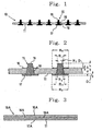
- Fig. 49 is a cross-sectional view illustrating the construction of a conventional exemplary probe for circuit inspection, which is equipped with a circuit board for inspection, an anisotropically conductive sheet and a sheet-like connector.
- the circuit board 85 for inspection having, on one surface thereof, a great number of inspection electrodes 86 formed in accordance with a pattern corresponding to a pattern of electrodes to be inspected of a circuit board to be inspected.
- the sheet-like connector 90 is arranged on one surface of the circuit board 85 for inspection through the anisotropically conductive sheet 80.
- the anisotropically conductive sheet 80 is a sheet exhibiting conductivity only in its thickness-wise direction or having pressure-sensitive conductive conductor parts exhibiting conductivity only in its thickness-wise direction when it is pressurized in the thickness-wise direction.
- anisotropically conductive sheets those of various structures have been known.
- the following Prior Art 2 disclose an anisotropically conductive sheet (hereinafter referred to as "dispersion type anisotropically conductive sheet”) obtained by uniformly dispersing metal particles in an elastomer
- the following Prior Art 3 and the like disclose an anisotropically conductive sheet (hereinafter referred to as “uneven distribution type anisotropically conductive sheet”) obtained by unevenly distributing particles of a conductive magnetic substance in an elastomer to form a great number of conductive parts extending in a thickness-wise direction thereof and insulating parts for mutually insulating them.
- the following Prior Art 4 and the like disclose an uneven distribution type anisotropically conductive sheet with a difference in level defined between the surface of each conductive part and an insulating part.
- the sheet-like connector 90 has a flexible insulating sheet 91 composed of, for example a resin, and is formed by arranging, in this insulating sheet 91, a plurality of electrode structures 95 each extending in a thickness-wise direction of the insulating sheet in accordance with the pattern corresponding to the pattern of the electrodes to be inspected of the circuit board to be inspected.
- Each of the electrode structures 95 is formed by integrally connecting a projected front-surface electrode part 96 exposed to a front surface of the insulating sheet 91 and a plate-like back-surface electrode part 97 exposed to a back surface of the insulating sheet 91 to each other through a short circuit part 98 extending through in the thickness-wise direction of the insulating sheet 91.
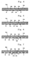
- Such a sheet-like connector 90 is generally produced in the following manner.
- a laminate material 90A obtained by forming a metal layer on one surface of an insulating sheet 91 is first provided, and through-holes 98H each extending through in a thickness-wise direction of the insulating sheet 91 are formed in the insulating sheet 91 as illustrated in Fig. 50(b) .
- a resist film 93 is then formed on the metal layer 92 on the insulating sheet 91, and an electroplating treatment is conducted by using the metal layer 92 as a common electrode, whereby metal deposit is filled into the through-holes 98H in the insulating sheet 91 to form short circuit parts 98 integrally joined to the metal layer 92, and at the same time, projected front-surface electrode parts 96 integrally joined to the respective short circuit parts 98 are formed on the front surface of the insulating sheet 91.
- the resist film 93 is removed from the metal layer 92, and as illustrated in Fig. 50(d) , a resist film 94A is formed on the surface of the insulating sheet 91 including the front-surface electrode parts 96, and moreover resist film portions 94B are formed on the metal layer 92 in accordance with a pattern corresponding to a pattern of back-surface electrode parts to be formed.
- the metal layer 92 is subjected to an etching treatment to remove exposed portions of the metal layer 92, thereby forming back-surface electrode parts 97 as illustrated in Fig. 50(e) , thus resulting in the formation of the electrode structures 95.
- the resist film 94A formed on the insulating sheet 91 and front-surface electrode parts 96 is removed, and at the same time the resist film portions 94B formed on the back-surface electrode parts 97 are removed, thereby obtaining the sheet-like connector 90.
- the front-surface electrode parts 96 of the electrode structures 95 in the sheet-like connector 90 are arranged on the surface of a circuit board to be inspected,for example, a wafer so as to be located on electrodes to be inspected of the wafer.
- the wafer is pressed by the probe for inspection, whereby the anisotropically conductive sheet 80 is pressed by the back-surface electrode parts 97 of the electrode structures 95 in the sheet-like connector 90, and in the anisotropically conductive sheet 80, conductive paths are thereby formed between the back-surface electrode parts 97 and the inspection electrodes 86 of the circuit board 85 for inspection in the thickness-wise direction of the anisotropically conductive sheet 80.
- electrical connection of the electrodes to be inspected of the wafer to the inspection electrodes 86 of the circuit board 85 for inspection is achieved.
- necessary electrical inspection as to the wafer is then performed.
- the anisotropically conductive sheet is deformed according to the degree of warpage of the wafer when the wafer is pressed by the probe for inspection, so that good electrical connection to a great number of the respective electrodes to be inspected in the wafer can be surely achieved.
- the metallic deposit by the electroplating isotropically grows. Therefore, in the resulting front-surface electrode part 96, a distance w from a periphery of the front-surface electrode part 96 to a periphery of the short circuit part 98 becomes equivalent to the projected height h of the front-surface electrode part 96 as illustrated in Fig. 51 . Accordingly, the diameter R of the resulting front-surface electrode part 96 exceeds twice of the projected height h and becomes considerably large.
- the growing rate of the metallic deposit varies with individual through-holes 98H in the insulating sheet 91 due to the unevenness of the current density distribution, so that a wide scatter occurs on the projected height h of the front-surface electrode parts 96 formed and the distance w from the periphery of the front-surface electrode part 96 to the periphery of the short circuit part 98, i.e., the diameter R. If a wide scatter occurs on the projected height h of the front-surface electrode parts 96, stable electrical connection to the circuit board to be inspected becomes difficult. If a wide scatter occurs on the diameter of the front-surface electrode parts 96 on the other hand, there is a possibility that adjacent front-surface electrode parts may short-circuit each other.
- a means of making the projected height h of the front-surface electrode parts 96 small, and a means of making the diameter (smallest length in the case where the sectional form is not circular) r of the short circuit parts 98 small, i.e., making the diameter of the through-holes 98H in the insulating sheet 91 small are considered as means for making the diameter of the resulting front-surface electrode parts 96 small.
- the sheet-like connector obtained by the former means however, it is difficult to surely achieve stable electrical connection to the electrodes to be inspected.
- the latter means the formation itself of the short circuit parts 98 and front-surface electrode parts 96 by the electroplating treatment becomes difficult.
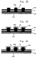
- a laminate material 90B obtained by forming a resist film 93A.and a front surface-side metal layer 92A on a front surface of an insulating sheet 91 in this order, and laminating a back surface-side metal layer 92B on a back surface of the insulating sheet 91 is provided.
- a laminate material 90B obtained by forming a resist film 93A.and a front surface-side metal layer 92A on a front surface of an insulating sheet 91 in this order, and laminating a back surface-side metal layer 92B on a back surface of the insulating sheet 91 is provided.
- Fig. 52(a) a laminate material 90B obtained by forming a resist film 93A.and a front surface-side metal layer 92A on a front surface of an insulating sheet 91 in this order, and laminating a back surface-side metal layer 92B on a back surface of the insulating sheet 91 is provided.
- a plating treatment is then conducted by using the front surface-side metal layer 92A in the laminate material 90B as an electrode, thereby filling a metal into the recesses 90K for forming electrode structures to form front-surface electrode parts 96 and short circuit parts 98.
- the back surface-side metal layer in the laminate material is then subjected to an etching treatment to remove a part thereof, thereby forming back-surface electrode parts 97 as illustrated in Fig. 52(d) , thus resulting in provision of the sheet-like connector.
- a laminate material 90C obtained by forming a front surface-side metal layer 92A on a front surface of an insulating sheet material 91A having a thickness greater than that of an insulating sheet in a sheet-like connector to be formed and laminating a back surface-side metal layer 92B on a back surface of the insulating sheet material 91A is provided.
- a laminate material 90C obtained by forming a front surface-side metal layer 92A on a front surface of an insulating sheet material 91A having a thickness greater than that of an insulating sheet in a sheet-like connector to be formed and laminating a back surface-side metal layer 92B on a back surface of the insulating sheet material 91A is provided.
- Fig. 53(a) a laminate material 90C obtained by forming a front surface-side metal layer 92A on a front surface of an insulating sheet material 91A having a thickness greater than that of an insulating sheet in a sheet-like connector to be formed
- through-holes each linked to each of the back surface-side metal layer 92B and insulating sheet material 91A in the laminate material 90C and extending in a thickness-wise direction of the laminate material are formed, thereby forming, in the back surface of the laminate material 90C, recesses 90K for forming electrode structures, which each have a tapered form fitted to a short circuit part and a front-surface electrode part of an electrode structure to be formed.
- a plating treatment is then conducted by using the front surface-side metal layer 92A in the laminate material 90C as an electrode, thereby filling a metal into the recesses 90K for forming electrode structures as illustrated in Fig. 53(c) to form front-surface electrode parts 96 and short circuit parts 98.
- the front surface-side metal layer 92A in the laminate material 90C is removed, and the insulating sheet material 91A is subjected to an etching treatment to remove the portion on the front surface side of the insulating sheet material, thereby forming an insulating sheet 91 having a necessary thickness and exposing the front-surface electrode parts 96 as illustrated in Fig. 53(d) .
- the back surface-side metal layer 92B is then subjected to an etching treatment, thereby forming back-surface electrode parts, thus resulting in provision of the sheet-like connector.
- the front-surface electrode parts small in diameter and high in projected height can be formed in a state that a clearance between front-surface electrodes of electrode structures adjacent to each other has been sufficiently retained, since the front-surface electrode parts are in a tapered form.
- the front-surface electrode parts of the respective electrode structures are formed by using the recesses for forming the electrode structures formed in the laminate material as cavities, so that the electrode structures narrow in a scatter of projected height of the front-surface electrode parts can be provided.
- the diameter of the front-surface electrode parts in the electrode structures is equivalent to or smaller than the diameter of the short circuit parts, i.e., the diameter of the through-holes formed in the insulating sheet, so that the electrode structures fall off from the back surface of the insulating sheet, resulting in the difficulty of actually using such a sheet-like connector.
- the present invention has been made on the basis of the foregoing circumstances and has as a first object the provision of a sheet-like connector as defined in claim 10 that electrode structures each having a front-surface electrode part small in diameter can be formed, and a stable electrically connected state can be surely achieved even to a circuit device, on which electrodes have been formed at a small pitch, and the electrode structures are prevented from falling off from an insulating sheet to achieve high durability.
- a second object of the present invention is to provide a process as defined in claim 1 or 6 capable of producing a sheet-like connector that electrode structures each having a front-surface electrode part small in diameter and narrow in a scatter of projected height thereof can be formed, and stable electrically connected state can be surely achieved even to a circuit device, on which electrodes have been formed at a small pitch, and the electrode structures are prevented from falling off from an insulating sheet to achieve high durability.
- a third object of the present invention is to provide a probe for circuit inspection as defined in claim 10, which is equipped with the above-described sheet-like connector.
- a fourth object is to provide an inspection apparatus for circuit devices, which is equipped with the above-described probe for circuit inspection.
- the holding part continuously extending from a base end portion of the front-surface electrode part outward along the front surface of the insulating sheet is formed in each of the electrode structure, so that the electrode structures are prevented from falling off from the insulating sheet to achieve high durability even when the diameter of the front-surface electrode parts is small.
- the front-surface electrode parts small in diameter can be formed, whereby a clearance between adjacent front-surface electrodes can be surely retained, and so flexibility by virtue of the insulating sheet can be sufficiently exhibited. As a result, a stable electrically connected state can be surely achieved even to a circuit device, on which electrodes have been formed at a small pitch.
- the recesses for forming the electrode structures are formed in the laminate material having the insulating sheet in advance, and the front-surface electrode parts are formed by using the recesses for forming the electrode structures as cavities, so that the front-surface electrode parts small in diameter and narrow in a scatter of the projected height can be provided.
- the holding parts continuously extending from the base end portion of the front-surface electrode part outward along the front surface of the insulating sheet can be surely formed by subjecting the front surface-side metal layer formed on the front surface of the insulating sheet to an etching treatment, so that a sheet-like connector has a high durability as the electrode structures are prevented from falling off from the insulating sheet can be produced even when the diameter of the front-surface electrode parts is small.
- the above-described sheet-like connector is provided, so that a stable electrically connected state can be surely achieved even to a circuit device, on which electrodes have been formed at a small pitch.
- the electrode structures in the sheet-like connector are prevented from falling off, high durability is achieved.
- the above-described probe for circuit inspection is provided, so that a stable electrically connected state can be surely achieved even to a circuit device, on which electrodes have been formed at a small pitch.
- inspection can be performed with high reliability over a long period of time even when the inspection is conducted as to a great number of circuit devices.
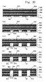
- Fig. 1 is a cross-sectional view illustrating the construction of a first exemplary sheet-like connector according to the present invention
- Fig. 2 is a cross-sectional view illustrating, on an enlarged scale, electrode structures in the first exemplary sheet-like connector.
- the first exemplary sheet-like connector 10 is used in a probe for conducting electrical inspection of circuit devices and has a flexible insulating sheet 11.
- a plurality of electrode structures 15 composed of a metal and extending in a thickness-wise direction of the insulating sheet 11 are arranged in a state separated from one another in a plane direction of the insulating sheet 11 in accordance with a pattern corresponding to a pattern of electrodes to be inspected of a circuit device that is an object of inspection.
- Each of the electrode structures 15 is composed of a protruding front-surface electrode part 16 exposed to a front surface of the insulating sheet 11 and projected from the front surface of the insulating sheet 11, a rectangular flat plate-like back-surface electrode part 17 exposed to a back surface of the insulating sheet 11, a short circuit part 18 continuously extending from the base end of the front-surface electrode part 16 through the insulating sheet 11 in the thickness-wise direction thereof and linked to the back-surface electrode part 17, and a circular ring plate-like holding part 19 continuously extending from a peripheral surface of a base end portion of the front-surface electrode part 16 outward and radially along the front surface of the insulating sheet 11.
- each front-surface electrode part 16 is formed continuously with the short circuit part 18 in a tapered form that the diameter becomes gradually small as it goes toward a tip end from a base end thereof, i.e., formed in a truncated cone form as a whole, and the short circuit part 18 continuous with the base end of the front-surface electrode part 16 is formed in a tapered form that the diameter becomes gradually small as it goes toward one surface from the other surface of the insulating sheet 11, i.e., formed in a truncated cone form as a whole.
- the diameter R 1 of the base end of the front-surface electrode part 16 is the same as the diameter R 3 of an end of the short circuit part 18 continuous with this base end.
- the insulating sheet 11 has insulating property and is flexible.
- a resin sheet formed of a polyamide resin, liquid crystal polymer, polyester, fluororesin or the like, or a sheet obtained by impregnating a cloth woven by fibers with any of the above-described resins may be used.
- the insulating sheet is preferably composed of an etching-capable material in that through-holes for forming the short circuit parts 18 can be easily formed by etching with polyimide being particularly preferred.
- the thickness d of the insulating sheet 11 is flexible. However, it is preferably 10 to 50 ⁇ m, more preferably 10 to 25 ⁇ m.
- the electrode structures 15 may be used nickel, copper, gold, silver, palladium, iron or the like.
- the electrode structures 15 may be any of those formed of a simple metal, those formed of an alloy of at least two metals and those obtained by laminating at least two metals as a whole.
- a film of a chemically stable metal having high conductivity, such as gold, silver or palladium may be formed in order that oxidation of the electrode parts may be prevented, and electrode parts small in contact resistance may be provided.
- a ratio (R 2 /R 1 ) of the diameter R 2 of the tip end of the front-surface electrode part 16 to the diameter R 1 of the base end is preferably 0.11 to 0.55, more preferably 0.15 to 0.4.
- the diameter R 1 of the base end of the front-surface electrode part 16 is preferably 30 to 70%, more preferably 35 to 60% of the pitch of the electrode structures 15.
- a ratio h/R 1 of the projected height h of the front-surface electrode part 16 to the diameter R 1 of the base end thereof is preferably 0.2 to 0.8, more preferably 0.25 to 0.6.
- the diameter R 1 of the base end of the front-surface electrode part 16 is preset in consideration of the above-described conditions, the diameter of its corresponding electrode to be connected, and the like. However, it is, for example, preferably 30 to 80 ⁇ m, more preferably 30 to 50 ⁇ m.
- the projected height h of the front-surface part 16 is preferably 15 to 50 ⁇ m, more preferably 15 to 30 ⁇ m in that stable electrical connection to its corresponding electrode to be connected can be achieved.
- each back-surface electrode part 17 is only required to be greater than the diameter R 4 of the other end of the short circuit part 18 linked to the back-surface electrode part 17 and smaller than the pitch of the electrode structures 15 and is preferably great as much as possible. Stable electrical connection can be thereby achieved with certainty even to, for example, the anisotropically conductive sheet.
- the thickness D 2 of the back-surface electrode part 17 is preferably 10 to 40 ⁇ m, more preferably 15 to 35 ⁇ m in that sufficiently high strength and excellent repetitive durability are achieved.
- a ratio R 3 /R 4 of the diameter R 3 of one end of the short circuit part 18 to the diameter R 4 of the other end thereof is preferably 0.45 to 1, more preferably 0.7 to 0.9.
- the diameter R 3 of one end of the short circuit part 18 is preferably 30 to 70%, more preferably 35 to 60% of the pitch of the electrode structures 15.
- the diameter R 6 of each holding part 19 is preferably 30 to 70%, more preferably 40 to 60% of the pitch of the electrode structures 15.
- the thickness D 1 of the holding part 19 is preferably 3 to 12 ⁇ m, more preferably 5 to 9 ⁇ m.
- the holding part 19 continuously extending from the base end portion of the front-surface electrode part 16 outward along the front surface of the insulating sheet 11 is formed in each of the electrode structures 15, so that the electrode structures 15 are prevented from falling off from the back surface of the insulating sheet 11 to achieve high durability even when the diameter of the front-surface electrode parts 16 is small.
- the electrode structures each have the front-surface electrode part 16 small in diameter, whereby a clearance between adjacent front-surface electrodes 16 can be surely retained, and so flexibility by virtue of the insulating sheet 11 can be sufficiently exhibited. As a result, a stable electrically connected state can be surely achieved even to a circuit device, on which electrodes have been formed at a small pitch.
- the above-described first exemplary sheet-like connector 10 can be produced, for example, in the following manner.
- a laminate material 10A composed of an insulating sheet 11, a first front surface-side metal layer 19A formed on a front surface of the insulating sheet 11, an insulating layer 16B formed on the surface of the first front surface-side metal layer 19A, a second front surface-side metal layer 16A formed on the surface of the insulating layer 16B, and a back surface-side metal layer 17A formed on a back surface of the insulating sheet 11 is first provided.
- the first front surface-side metal layer 19A is formed so as to have a thickness equivalent to the thickness of a holding part 19 in each of electrode structures 15 to be formed
- the insulating layer 16B is formed in such a manner that the total thickness of a thickness of the insulating layer 16B and the thickness of the first front surface-side metal layer 19A is equivalent to the projected height of a front-surface electrode part 16 in the electrode structure 15 to be formed
- the back surface-side metal layer 17A is formed so as to have a thickness smaller than the thickness of a back-surface electrode part 17 in the electrode structure 15 to be formed.
- a polymeric material capable of being etched is preferably used, with polyimide being more preferred.
- a polymeric material capable of being etched is preferably used, with polyimide being more preferred.
- Such a laminate material 10A can be obtained by providing a laminated polyimide sheet with metal layers composed of, for example, copper laminated on both sides thereof and a laminated thermoplastic polyimide sheet with a metal layer composed of, for example, copper laminated on one side thereof, which are both generally marketed, arranging them in such a manner that a surface of the laminated thermoplastic polyimide sheet, on which metal layer is not laminated, faces the surface of one metal layer of the laminated polyimide sheet, and subjecting both sheets to a pressure-bonding treatment under heat.
- a resist film 12A for etching is formed on the whole surface of the second front surface-side metal layer 16A, and a resist film 13 for etching, in which a plurality of patterned holes 13K have been formed in accordance with a pattern corresponding to a pattern of the electrode structures 15 to be formed, is formed on the surface of the back surface-side metal layer 17A.
- materials for forming the resist films 12A and 13 may be used various materials used as photoresists for etching.
- Exposed portions of the back surface-side metal layer 17A are then subjected to an etching treatment through the respective patterned holes 13K in the resist film 13 to remove such portions, thereby forming, in the back surface-side metal layer 17A, a plurality of through-holes 17H linked to the respective patterned holes 13K in the resist film 13 as illustrated in Fig. 5 .
- exposed portions of the insulating sheet 11 are subjected to an etching treatment through the respective patterned holes 13K in the resist film 13 and the respective through-holes 17H in the back surface-side metal layer 17A to remove such portions, thereby forming, in the insulating sheet 11, a plurality of tapered through-holes 11H, the diameter of which becomes gradually small from the back surface of the insulating sheet 11 toward the front surface thereof, and each of which are linked to the through-holes 17K in the back surface-side metal layer 17A as illustrated in Fig. 6 .
- exposed portions of the first front surface-side metal layer 19A are subjected to an etching treatment through the respective patterned holes 13K in the resist film 13, the respective through-holes 17H in the back surface-side metal layer 17A and the respective through-holes 11H in the insulating sheet 11 to remove such portions, thereby forming, in the first front surface-side metal layer 19A, a plurality of through-holes 19H each linked to the through-holes 11H in the insulating sheet 11 as illustrated in Fig. 7 .
- exposed portions of the insulating layer 16B are subjected to an etching treatment through the respective patterned holes 13K in the resist film 13, the respective through-holes 17H in the back surface-side metal layer 17A, the respective through-holes 11H in the insulating sheet 11 and the respective through-holes 19H in the first front surface-side metal layer 19A to remove such portions, thereby forming, in the insulating layer 16B, a plurality of tapered through-holes 16H, the diameter of which becomes gradually small from the back surface of the insulating layer 16B toward the front surface thereof, and each of which are linked to the respective through-holes 19H in the first front surface-side metal layer 19A as illustrated in Fig. 8 .
- a plurality of recesses 10K for forming electrode structures each linked with the respective through-holes 17H in the back surface-side metal layer 17A, the respective through-holes 11H in the insulating sheet 11, the respective through-holes 19H in the first front surface-side metal layer 19A and the respective through-holes 16H in the insulating layer 16B linked to one another are thereby formed in the back surface of the laminate material 10A.
- Etchants for etching the back surface-side metal layer 17A and the first front surface-side metal layer in the above-described process are suitably selected according to the materials forming these metal layers.
- these metal layers are composed of, for example, copper, an aqueous solution of ferric chloride may be used.
- an etchant for etching the insulating sheet 11 and the insulating layer 16B may be used an aqueous hydrazine solution.
- the tapered through-holes 11H and 16H, the diameter of which becomes gradually small from the back surface toward the front surface, can be formed in the insulating sheet 11 and the insulating layer 16B, respectively, by selecting conditions for the etching treatments.
- a resist film 12B for plating is formed on the laminate material 10A so as to cover the whole surface of the second front surface-side metal layer 16A, and a resist film 14A for plating, in which a plurality of patterned holes 14K have been formed in accordance with a pattern corresponding to a pattern of back-surface electrode parts 17 in the electrode structures 15 to be formed, is formed on the surface of the back surface-side metal layer 17A.
- materials for forming the resist films 12B and 14A may be used various materials used as photoresists for plating.
- the laminate material 10A is then subjected to an electroplating treatment by using the second front surface-side metal layer 16A as an electrode to fill a metal into the respective recesses 10K for forming electrode structures and the respective patterned holes 14K in the resist film 14A, thereby forming a plurality of protruding front-surface electrode parts 16 projected from the front surface of the insulating sheet 11, short circuit parts 18 continuously extending from the respective base ends of the front-surface electrode parts 16 through the insulating sheet 11 in a thickness-wise direction thereof, and back-surface electrode parts 17 respectively linked to the other ends of the short circuit parts 18 as illustrated in Fig. 10 .
- the back-surface electrode parts 17 are in a state connected to one another through the back surface-side metal layer 17A.
- a patterned resist film 14B for etching is formed so as to cover the back-surface electrode parts 17 to subject the second front surface-side metal layer 16A and the back surface-side metal layer 17A to an etching treatment, thereby removing the whole of the second front surface-side metal layer 16A and exposed portions of the back surface-side metal layer as illustrated in Fig. 12 to form a plurality of back-surface electrode parts 17 separated from one another.
- the insulating layer 16B is then subjected to an etching treatment to remove the whole thereof, and the resist film 14B is removed, thereby exposing the front-surface electrode parts 16, first front surface-side metal layer 19A and back-surface electrode parts 17 as illustrated in Fig. 13 .
- a patterned resist film 12C for etching is formed so as to cover the front-surface electrode parts 16 and portions to become holding parts 19 in the first front surface-side metal layer 19A, and a resist film 14C for etching is formed so as to cover the back surface of the insulating sheet 11 and all of the back-surface electrode parts 17.
- the first front surface-side metal layer 19A is then subjected to an etching treatment to remove exposed portions, thereby forming holding parts 19 each continuously extending from a peripheral surface of a base end portion of the front-surface electrode part 16 outward and radially along the front surface of the insulating sheet 11, thus resulting in the formation of the electrode structures 15.
- the resist films 12C is then removed from the front-surface electrode parts 16 and holding parts 19, and the resist film 14C is removed from the back surface of the insulating sheet 11 and the back-surface electrode parts 17, thereby obtaining the sheet-like connector 10 shown in Fig. 1 .
- the recesses 10K for forming the electrode structures are formed in the laminate material 10A having the insulating sheet 11 in advance, and the front-surface electrode parts 16 are formed by using the recesses 10K for forming the electrode structures as cavities, so that the front-surface electrode parts 16 small in diameter and narrow in a scatter of the projected height thereof can be provided.
- the holding parts 19 each continuously extending from the base end portion of the front-surface electrode part 16 outward along the front surface of the insulating sheet 11 can be surely formed by subjecting the front surface-side metal layer 19A formed on the front surface of the insulating sheet 11 to an etching treatment, so that the sheet-like connector 10 that has high durability as the electrode structures 15 are prevented from falling off from the insulating sheet 11 can be produced even when the diameter of the front-surface electrode parts 16 is small.
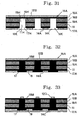
- Fig. 16 is a cross-sectional view illustrating the construction of a second exemplary sheet-like connector according to the present invention.
- the second exemplary sheet-like connector 10 is used in a probe for conducting electrical inspection of circuit devices and has a flexible insulating sheet 11.
- a plurality of electrode structures 15 composed of a metal and extending in a thickness-wise direction of the insulating sheet 11 are arranged in a state separated from one another in a plane direction of the insulating sheet 11 in accordance with a pattern corresponding to a pattern of electrodes to be inspected of a circuit device that is an object of inspection.
- Each of the electrode structures 15 is composed of a protruding front-surface electrode part 16 exposed to a front surface of the insulating sheet 11 and projected from the front surface of the insulating sheet 11, a rectangular flat plate-like back-surface electrode part 17 exposed to a back surface of the insulating sheet 11, a columnar short circuit part 18 continuously extending from the base end of the front-surface electrode part 16 through the insulating sheet 11 in the thickness-wise direction thereof and linked to the back-surface electrode part 17, and a circular ring plate-like holding part 19 continuously extending from a peripheral surface of a base end portion of the front-surface electrode part 16 outward and radially along the front surface of the insulating sheet 11.
- each front-surface electrode part 16 is formed in an almost semi-spherical shape that the diameter becomes small as it goes toward the tip thereof, and the diameter of the base end of the front-surface electrode part 16 is equivalent to the diameter of one end of the short circuit part 18 continuous with the base end.
- the above-described second exemplary sheet-like connector 10 can be produced, for example, in the following manner.
- a laminate material 10B composed of an insulating sheet 11 formed of a polymeric material capable being etched, for example, polyimide, a front surface-side metal layer 19B formed on a front surface of the insulating sheet 11, an insulating layer 16B formed on the surface of the front surface-side metal layer 19B, a back surface-side metal layer 17A formed on a back surface of the insulating sheet 11, and a resist film 13A. formed on the back surface-side metal layer 17A is first provided.
- a polymeric material capable being etched for example, polyimide
- the front surface-side metal layer 19B is formed so as to have a thickness equivalent to the thickness of a holding part 19 in each of electrode structures 15 to be formed
- the insulating layer 16B is formed in such a manner that the total thickness of a thickness of the insulating layer 16B and the thickness of the first front surface-side metal layer 19B is equivalent to the projected height of a front-surface electrode part 16 in the electrode structure 15 to be formed
- the back surface-side metal layer 17A is formed so as to have a thickness equivalent to the thickness of a back-surface electrode part 17 in the electrode structure 15 to be formed.
- the insulating layer 16B is then subjected to photolithography (exposing treatment and developing treatment), thereby forming a plurality of through-holes 16H in the insulating layer 16B in accordance with a pattern corresponding to a pattern of front-surface electrode parts 16 in the electrode structures 15 to be formed as illustrated in Fig. 18 .
- Exposed portions of the front surface-side metal layer 19B are then subjected to an etching treatment through the respective through-holes 16H in the insulating layer 16B to remove such portions, thereby forming, in the front surface-side metal layer 19B, a plurality of through-holes 19H each linked to the respective through-holes 16H in the insulating layer 16B as illustrated in Fig. 19 .
- Exposed portions of the insulating sheet 11 are then subjected to an etching treatment through the respective through-holes 16H in the insulating layer 16B and the respective through-holes 19H in the front surface-side metal layer 19B to remove such portions, thereby forming, in the insulating sheet 11, a plurality of through-holes 11H each linked to the respective through-holes 19H in the front surface-side metal layer 19B as illustrated in Fig. 20 .
- a plurality of recesses 10K for forming electrode structures with the respective through-holes 16H in the insulating layer 16B, the respective through-holes 19H in the front surface-side metal layer 19B and the respective through-holes 11H in the insulating sheet 11 linked to one another are thereby formed in the front surface of the laminate material 10B.
- the laminate material 10B in which the recesses 10K for forming electrode structures have been formed in such a manner, is subjected to an electroplating treatment by using the back surface-side metal layer 17A as an electrode to fill a metal into the respective recesses 10K for forming electrode structures, thereby forming a plurality of columnar conductors 16M for front-surface electrode parts, which are projected from the front surface of the insulating sheet 11, and short circuit parts 18 continuously extending from the respective base ends of the conductors 16M for front-surface electrode parts through the insulating sheet 11 in a thickness-wise direction thereof and linked to the back surface-side metal layer 17A as illustrated in Fig. 21 .
- the insulating layer 16B is removed from the laminate material 10B, in which the conductors 16M for front-surface electrode parts, short circuit parts 18 have been formed in such a manner, thereby exposing the conductors 16M for front-surface electrode parts and front surface-side metal layer 19B as illustrated in Fig. 22 .
- a patterned resist film 13B is then formed so as to cover the conductors 16M for front-surface electrode parts and portions to become holding parts 19 in the front surface-side metal layer 19B as illustrated in Fig. 23 .
- the front surface-side metal layer 19B is then subjected to an etching treatment to remove exposed portions, thereby forming holding parts 19 each continuously extending from a peripheral surface of a base end portion of the conductor 16M for front-surface electrode part outward and radially along the front surface of the insulating sheet 11 as illustrated in Fig. 24 .
- an electrolytic etching treatment is conducted to shape the respective conductors 16M for front-surface electrode parts, thereby forming front-surface electrode parts 16 each having a top portion in an almost semi-spherical form as illustrated in Fig. 25 .
- the resist film 13A on the back surface of the insulating sheet 11 is then subjected to photolithography, thereby forming a patterned resist film 13D so as to cover portions to become back-surface electrode parts in the back surface-side metal layer 17A and forming a resist film 13C so as to cover the front surface of the insulating sheet 11, the front-surface electrode parts 16 and the holding parts 19 as illustrated in Fig. 26 .
- the back surface-side metal layer 17A is then subjected to an etching treatment to remove exposed portions, thereby forming back-surface electrode parts 17 respectively linked to the other ends of the short circuit parts 18 as illustrated in Fig. 27 , thus resulting in the formation of the electrode structures 15.
- the resist film 13C is then removed from the insulating sheet 11, front-surface electrode parts 16 and holding part 19, and the resist film 13D is removed from the back-surface electrode parts 17, thereby obtaining the second exemplary sheet-like connector 10 shown in Fig. 16 .
- Fig. 28 is a cross-sectional view illustrating the construction of a third exemplary sheet-like connector according to the present invention.
- the third exemplary sheet-like connector 10 is used in a probe for conducting electrical inspection of circuit devices and has a flexible insulating sheet 11.
- a plurality of electrode structures 15 composed of a metal and extending in a thickness-wise direction of the insulating sheet 11 are arranged in a state separated from one another in a plane direction of the insulating sheet 11 in accordance with a pattern corresponding to a pattern of electrodes to be inspected of a circuit device that is an object of inspection.
- Each of the electrode structures 15 is composed of a protruding front-surface electrode part 16 exposed to a front surface of the insulating sheet 11 and projected from the front surface of the insulating sheet 11, a back-surface electrode part 17 exposed to a back surface of the insulating sheet 11, a columnar short circuit part 18 continuously extending from the base end of the front-surface electrode part 16 through the insulating sheet 11 in the thickness-wise direction thereof and linked to the back-surface electrode part 17, and a circular ring plate-like holding part 19 continuously extending from a peripheral surface of a base end portion of the front-surface electrode part 16 outward and radially along the front surface of the insulating sheet 11.
- the front-surface electrode part 16 has an almost semi-spherical central portion, the diameter of which becomes small toward the tip end side from the base end side thereof, and an almost semi-spherical tip portion having a diameter smaller than the diameter of the central portion, the diameter of which becomes small toward the tip.
- the diameter of the base end of the front-surface electrode part 16 is equivalent to the diameter of one end of the short circuit part 18 continuous with the base end.
- the back-surface electrode part 17 has a rectangular flat plate-like base portion and a rectangular flat plate-like tip portion projected from this base portion and a size smaller than the base portion.
- the above-described third exemplary sheet-like connector 10 can be produced, for example, in the following manner.
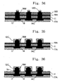
- a laminate material 10A composed of an insulating sheet 11 formed of a polymeric material capable of being etched, for example, polyimide, a first front surface-side metal layer 19A formed on a front surface of the insulating sheet 11, an insulating layer 16B formed on the surface of the first front surface-side metal layer 19A and formed of a polymeric material capable of being etched, for example, polyimide, a second front surface-side metal layer 16A formed on the surface of the insulating layer 16B, and a back surface-side metal layer 17A formed on a back surface of the insulating sheet 11 is first provided.
- a laminate material 10A composed of an insulating sheet 11 formed of a polymeric material capable of being etched, for example, polyimide, a first front surface-side metal layer 19A formed on a front surface of the insulating sheet 11, an insulating layer 16B formed on the surface of the first front surface-side metal layer 19A and formed of a polymeric material capable of being etched, for example, polyimi
- the first front surface-side metal layer 19A is formed so as to have a thickness equivalent to the thickness of a holding part 19 in each of electrode structures 15 to be formed
- the insulating layer 16B is formed so as to have a thickness equivalent to the thickness (height) of the central portion of the front-surface electrode part 19 in the electrode structure 15 to be formed
- the second front surface-side metal layer 16A is formed so as to have a thickness equivalent,to the thickness (height) of the tip portion of the front-surface electrode part 19 in the electrode structure 15 to be formed
- the back surface-side metal layer 17A is formed so as to have a thickness equivalent to a base portion of a back-surface electrode part 17 in the electrode structure 15 to be formed.
- a resist film 12A for etching is formed on the whole surface of the second front surface-side metal layer 16A, and a resist film 13 for etching, in which a plurality of patterned holes 13K have been formed in accordance with a pattern corresponding to a pattern of the electrode structures 15 to be formed, is formed on the surface of the back surface-side metal layer 17A.
- Exposed portions of the back surface-side metal layer 17A are then subjected to an etching treatment through the respective patterned holes 13K in the resist film 13 to remove such portions, thereby forming a plurality of through-holes 17H in the back surface-side metal layer 17A as illustrated in Fig. 30(b) .
- exposed portions of the insulating sheet 11 are subjected to an etching treatment through the respective patterned holes 13K in the resist film 13 and the respective through-holes 17H in the back surface-side metal layer 17A to remove such portions, thereby forming, in the insulating sheet 11, a plurality of through-holes 11H each linked to the respective through-holes 17H in the back surface-side metal layer 17A as illustrated in Fig.
- first front surface-side metal layer 19A is subjected to an etching treatment through the respective patterned holes 13K in the resist film 13, the respective through-holes 17H in the back surface-side metal layer 17A and the respective through-holes 11H in the insulating sheet 11 to remove such portions, thereby forming, in the first front surface-side metal layer 19A, a plurality of through-holes 19H each linked to the respective through-holes 11H in the insulating sheet 11 as illustrated in Fig. 30(d) .
- exposed portions of the insulating layer 16B are subjected to an etching treatment through the respective patterned holes 13K in the resist film 13, the respective through-holes 17H in the back surface-side metal layer 17A, the respective through-holes 11H in the insulating sheet 11 and the respective through-holes 19H in the first front surface-side metal layer 19A to remove such portions, thereby forming, in the insulating layer 16B, a plurality of through-holes 16H each linked to the respective through-holes 19H in the first front surface-side metal layer 19A as illustrated in Fig. 30(e) .
- a plurality of recesses 10K for forming electrode structures with the respective through-holes 17H in the back surface-side metal layer 17A, the respective through-holes 11H in the insulating sheet 11, the respective through-holes 19H in the first front surface-side metal layer 19A and the respective through-holes 16H in the insulating layer 16B linked to one another are thereby formed in the back surface of the laminate material 10A.
- a resist film 12B for plating is formed on the laminate material 10A so as to cover the whole surface of the second front surface-side metal layer 16A, and a resist film 14A for plating, in which a plurality of patterned holes 14K have been formed in accordance with a pattern corresponding to a pattern of back-surface electrode parts 17 in the electrode structures 15 to be formed, is formed on the surface of the back surface-side metal layer 17A.
- the laminate material 10A is then subjected to an electroplating treatment by using the second front surface-side metal layer 16A as an electrode to fill a metal into the respective recesses 10K for forming electrode structures and the respective patterned holes 14K in the resist film 14A, thereby forming a plurality of protruding conductors 16M for front-surface electrode parts projected from the front surface of the insulating sheet 11, short circuit parts 18 continuously extending from the respective base ends of the conductors 16M for front-surface electrode parts through the insulating sheet 11 in a thickness-wise direction thereof, and back-surface electrode parts 17 respectively linked to the other ends of the short circuit parts 18 as illustrated in Fig. 32 .
- each of the conductors 16M for front-surface electrode parts are in a state connected to one another through the second front surface-side metal layer 16A, and each of the back-surface electrode parts 17 are in a state connected to one another through the back surface-side metal layer 17A.
- a resist film 14C for etching is formed so as to cover the back-surface electrode parts 17 and back surface-side metal layer 17A, and a patterned resist film 12D for etching is formed on the surface of the second front surface-side metal layer 16A in accordance with a pattern corresponding to a pattern of the tip portions of the front-surface electrode parts 16 to be formed to subject the second front surface-side metal layer 16A to an etching treatment, thereby removing exposed portions to form a plurality of conductors 16M for front-surface electrode parts, which each have a columnar central portion and a tip portion having a diameter smaller than the diameter of the central portion and are separated from one another, as illustrated in Fig. 34 .
- the resist film 12D is then removed, and the insulating layer 16B is subjected to an etching treatment to remove the whole thereof, thereby exposing the conductors 16M for front-surface electrode parts and the first front surface-side metal layer 19A. Thereafter, as illustrated in Fig. 35 , a patterned resist film 12C for etching is formed so as to cover the conductors 16M for front-surface electrode parts and portions to become holding parts 19 in the first front surface-side metal layer 19A.
- the first front surface-side metal layer 19A is then subjected to an etching treatment to remove exposed portions, thereby forming a plurality of holding parts 19 each continuously extending from a peripheral surface of a base end portion of the conductor 16M for front-surface electrode part outward and radially along the front surface of the insulating sheet 11 as illustrated in Fig. 36 .
- an electrolytic etching treatment is conducted to shape the conductors 16M for front surface electrode parts, thereby forming front surface electrode parts 16 each having an almost semi-spherical central portion and an almost semi-spherical tip portion projected from the central portion as illustrated in Fig. 37 .
- the resist film 14C is then subjected to photolithography, thereby forming a patterned resist film 14B for etching so as to cover the back-surface electrode parts 17 as illustrated in Fig. 38 , and a resist film 12E for etching is formed so as to cover the front surface of the insulating sheet 11, the front-surface electrode parts 16 and the holding parts 19 to subject the back surface-side metal layer 17A to an etching treatment, thereby removing exposed portions to form a plurality of back-surface electrode parts 17 separated from one another as illustrated in Fig. 39 , thus resulting in the formation of the electrode structures 15.
- the resist films 12E and 14B are then removed, thereby obtaining the third exemplary sheet-like connector 10 shown in Fig. 28 .
- Fig. 40 is a cross-sectional view illustrating the construction of a fourth exemplary sheet-like connector according to the present invention.
- the fourth exemplary sheet-like connector 10 has the same construction as that of the second sheet-like connector except that the electrode structures 15 each has a columnar front-surface electrode part 16, and can be produced in the same manner as the production process of the second sheet-like connector except that the conductors for front-surface electrode parts are provided as the front-surface electrode parts 16 without conducting an electrolytic etching treatment to the conductors for front-surface electrode parts as they are.
- Fig. 41 is a cross-sectional view illustrating the construction of an exemplary inspection apparatus for circuit devices.
- This inspection apparatus for circuit devices is suitable for respectively conducting electrical inspection of a plurality of integrated circuits formed on a wafer in a state of the wafer.
- This inspection apparatus for circuit devices has a probe 1 for circuit inspection for conducting electrical connection between respective electrodes 7 to be inspected of a wafer 6, which is a circuit device to be inspected, and a tester.
- this probe 1 for circuit inspection has a circuit board 20 for inspection, on the front surface (lower surface in the drawing) of which a plurality of inspection electrodes 21 have been formed in accordance with a pattern according to a pattern of the electrodes 7 to be inspected in all integrated circuits formed on the wafer 6.
- An anisotropically conductive connector 30 is arranged on the front surface of the circuit board 20 for inspection, and the sheet-like connector 10 of the construction shown in Fig.
- a pressurizing plate 3 for pressurizing the probe 1 for circuit inspection downward.
- a heater 5 is connected to both pressurizing plate 3 and wafer-mounting table 4.
- the circuit board 20 for inspection may be used any of conventionally known various materials for boards, and specific examples thereof include composite resin materials such as glass fiber-reinforced epoxy resins, glass fiber-reinforced phenol resins, glass fiber-reinforced polyimide resins and glass fiber-reinforced bismaleimide triazine resins, and ceramic materials such as glass, silicon dioxide and alumina.
- composite resin materials such as glass fiber-reinforced epoxy resins, glass fiber-reinforced phenol resins, glass fiber-reinforced polyimide resins and glass fiber-reinforced bismaleimide triazine resins, and ceramic materials such as glass, silicon dioxide and alumina.
- Such a board material include Pyrex (trademark) glass, quartz glass, alumina, beryllia, silicon carbide, aluminum nitride and boron nitride.
- the anisotropically conductive connector 30 is formed by a frame plate 31, in which a plurality of openings 32 have been formed correspondingly to electrode regions, in which electrodes to be inspected in the whole of the integrated circuits formed on the wafer, which is a circuit device to be inspected, have been arranged, and a plurality of anisotropically conductive sheets 35 arranged so as to close the respective openings in the frame plate 31 and fixed to and supported by respective opening edges of the frame plate 31.
- a material for forming the frame plate 31 so far as it has such stiffness as the resulting frame plate 31 is hard to be deformed, and the shape thereof is stably retained.
- various kinds of materials such as metallic materials, ceramic materials and resin materials may be used.
- an insulating film may be formed on the surface of the frame plate 31.
- the metallic material for forming the frame plate 31 include metals such as iron, copper, nickel, chromium, cobalt, magnesium, manganese, molybdenum, indium, lead, palladium, titanium, tungsten, aluminum, gold, platinum and silver, and alloys or alloy steels composed of a combination of at least two of these metals.
- resin material forming the frame plate 31 include liquid crystal polymers and polyimide resins.
- the material for forming the frame plate 31 preferably has a coefficient of linear thermal expansion of at most 3 x 10 -5 /K, more preferably -1 x 10 -7 to 1 x 10 -5 /K, particularly preferably 1 x 10 -6 to 8 x 10 -6 /K.
- Such a material include alloys or alloy steels of magnetic metals, such as invar alloys such as invar, Elinvar alloys such as Elinvar, superinvar, covar and 42 alloy.
- the thickness of the frame plate 31 so far as the shape thereof is retained, and the anisotropically conductive sheet 35 can be supported.
- the specific thickness thereof varies depending on the material, it is preferably, for example, 45 to 600 ⁇ m, more preferably 40 to 400 ⁇ m.
- Each of the anisotropically conductive sheets 35 is formed by an elastic polymeric substance and composed of a plurality of conductive parts 36 formed in accordance with a pattern corresponding to a pattern of electrodes 7 to be inspected in an electrode region formed on the wafer 6, which is a circuit board to be inspected, and each extending in a thickness-wise direction of the sheet, and insulating parts 37 mutually insulating these respective conductive parts 36.
- projected portions 38 protruding from other surfaces than portions, at which the conductive parts 36 and peripheral portions thereof are located, are formed at those portions on both sides of the anisotropically conductive sheet 35.
- conductive particles P exhibiting magnetism are contained at a high density in a state oriented so as to align in the thickness-wise direction.
- the insulating parts 37 do not contain the conductive particles P at all or scarcely contain them.
- the overall thickness (thickness of the conductive part 36 in the illustrated embodiment) of the anisotropically conductive sheet 35 is preferably 50 to 2,000 ⁇ m, more preferably 70 to 1,000 ⁇ m, particularly preferably 80 to 500 ⁇ m. When this thickness is 50 ⁇ m or greater, sufficient strength is imparted to such an anisotropically conductive sheet 35. When this thickness is 2,000 ⁇ m or smaller on the other hand, conductive parts 36 having necessary conductive properties are provided with certainty.
- the projected height of the projected portion 38 is preferably at least 10% in total of the thickness of the projected portion 38, more preferably at least 15%. Projected portions 38 having such a projected height are formed, whereby the conductive parts 36 are sufficiently compressed by small pressing force, so that good conductivity is surely achieved.
- the projected height of the projected portion 38 is preferably at most 100%, more preferably at most 70% of the shortest width or diameter of the projected portion 38. Projected portions 38 having such a projected height are formed, whereby the projected portions 38 are not buckled when they are pressurized, so that the prescribed conductivity is surely achieved.
- the elastic polymeric substance forming the anisotropically conductive sheet 35 is preferably a heat-resistant polymeric substance having a crosslinked structure.
- curable polymeric substance-forming materials usable for obtaining such a crosslinked polymeric substance various materials may be used. However, liquid silicone rubber is preferred.
- the liquid silicone rubber may be any of addition type and condensation type. However, addition type liquid silicone rubber is preferred.
- This addition type liquid silicone rubber is that cured by a reaction of a vinyl group with an Si-H bond and includes a one-pack type (one-component type) composed of polysiloxane having both vinyl group and Si-H bond and a two-pack type (two-component type) composed of polysiloxane having a vinyl group and polysiloxane having an Si-H bond.
- addition type liquid silicone rubber of the two-pack type is preferably used.
- the anisotropically conductive sheet 35 is formed by a cured product (hereinafter referred to as "cured silicon rubber") of the liquid silicone rubber
- the cured silicone rubber preferably has a compression set of at most 10%, more preferably at most 8%, still more preferably at most 6% at 150°C. If the compression set exceeds 10%, the conductive parts 36 tend to cause permanent set when the resulting anisotropically conductive connector is used repeatedly over many times or used repeatedly under high-temperature environment, whereby chains of the conductive particles P in the conductive parts 36 are disordered. As a result, it is difficult to retain the necessary conductivity.
- the compression set of the cured silicone rubber can be measured by a method in accordance with JIS K 6249.
- the cured silicone rubber preferably has a durometer A hardness of 10 to 60, more preferably 15 to 55, particularly preferably 20 to 50 at 23°C.
- the insulating parts 37 mutually insulating the conductive parts 36 are easily over-distorted when pressurized, and it may be difficult in some cases to retain the necessary insulating property between the conductive parts 36. If the durometer A hardness exceeds 60 on the other hand, pressurizing force by a considerably heavy load is required for giving proper distortion to the conductive parts 36, so that the wafer, which is a circuit board to be inspected, tends to cause great deformation or breakage.
- the conductive parts 36 tend to cause permanent set when the resulting anisotropically conductive connector is used repeatedly over many times, whereby chains of the conductive particles in the conductive parts 36 are disordered. As a result, it is difficult to retain the necessary conductivity.
- the cured silicone rubber for forming the anisotropically conductive sheet 35 preferably has a durometer A hardness of 25 to 40 at 23°C.
- the conductive parts 36 tend to cause permanent set when the WLBI test is conducted repeatedly, whereby chains of the conductive particles in the conductive parts 36 are disordered. As a result, it is difficult to retain the necessary conductivity.
- the durometer A hardness of the cured silicone rubber can be measured by a method in accordance with JIS K 6249.
- the cured silicone rubber preferably has tear strength of at least 8 kN/m, more preferably at least 10 kN/m, still more preferably at least 15 kN/m, particularly preferably at least 20 kN/m at 23°C. If the tear strength is lower than 8 kN/m, the resulting anisotropically conductive sheet 35 tends to deteriorate durability when it is distorted in excess.
- the tear strength of the cured silicone rubber can be measured by a method in accordance with JIS K 6249.
- a proper curing catalyst may be used for curing the addition type liquid silicone rubber.
- a curing catalyst may be used a platinum-containing catalyst.
- Specific examples thereof include publicly known catalysts such as platinic chloride and salts thereof, platinum-unsaturated group-containing siloxane complexes, vinylsiloxane-platinum complexes, platinum-1,3-divinyltetramethyldisiloxane complexes, complexes of triorganophosphine or phosphine and platinum, acetyl acetate platinum chelates, and cyclic diene-platinum complexes.
- the amount of the curing catalyst used is suitably selected in view of the kind of the curing catalyst and other curing treatment conditions. However, it is generally 3 to 15 parts by weight per 100 parts by weight of the addition type liquid silicone rubber.
- a general inorganic filler such as silica powder, colloidal silica, aerogel silica or alumina may be contained in the addition type liquid silicone rubber as needed.
- the conductive particles P contained in the conductive parts 36 may preferably be used particles obtained by coating the surfaces of core particles (hereinafter also referred to as "magnetic core particles") exhibiting magnetism with high-conductive metal.
- high-conductive metal means a metal having a conductivity of at least 5 x 10 6 ⁇ -1 m -1 at 0°C.
- the magnetic core particles for obtaining the conductive particles P preferably have a number average particle diameter of 3 to 40 ⁇ m.
- the number average particle diameter of the magnetic core particles means a value measured by a laser diffraction scattering method.
- the number average particle diameter is 3 ⁇ m or greater, conductive parts 36 easy to be deformed under pressure, low in resistance value and high in connection reliability can be easily obtained.
- the number average particle diameter is 40 ⁇ m or smaller on the other hand, minute conductive parts 36 can be easily formed, and the resultant conductive parts 36 tend to have stable conductivity.
- the magnetic core particles preferably have a BET specific surface area of 10 to 500 m 2 /kg, more preferably 20 to 500 m 2 /kg, particularly preferably 50 to 400 m 2 /kg.
- the BET specific surface area is 10 m 2 /kg or wider, such magnetic core particles can be surely plated in a required amount because an area capable of being plated in the magnetic core particles is sufficiently wide. Accordingly, conductive particles P high in conductivity can be obtained, and stable and high conductivity is achieved because a contact area between the conductive particles P is sufficiently wide.
- the BET specific surface area is 500 m 2 /kg or smaller on the other hand, such magnetic core particles do not become brittle, so that they are not broken when physical stress is applied, and stable and high conductivity is retained.
- the magnetic core particles preferably have a coefficient of variation of particle diameter of at most 50%, more preferably at most 40%, still more preferably at most 30%, particularly preferably at most 20%.
- the coefficient of variation of particle diameter is a value determined in accordance with the expression: ( ⁇ /Dn) x 100, wherein ⁇ is a standard deviation value of the particle diameter, and Dn is a number average particle diameter of the particles.
- a material for forming the magnetic core particles may be used iron, nickel, cobalt, a material obtained by coating such a metal with copper or a resin, or the like. Those having a saturation magnetization of at least 0.1 Wb/m 2 may be preferably used. The saturation magnetization thereof is more preferably at least 0.3 Wb/m 2 , particularly preferably at least 0.5 Wb/m 2 . Specific examples of the material include iron, nickel, cobalt and alloys thereof.
- the high-conductive metal applied to the surfaces of the magnetic core particles may be used gold, silver, rhodium, platinum, chromium or the like.
- gold is preferably used in that it is chemically stable and has a high electric conductivity.
- a proportion [(mass of high-conductive metal/mass of core particles) x 100] of the high-conductive metal to the core particles is at least 15 % by mass, preferably 25 to 35 % by mass.
- the proportion of the high-conductive metal is lower than 15 % by mass, the conductivity of such conductive particles P is markedly deteriorated when the resulting anisotropically conductive connector is used repeatedly under high-temperature environment. As a result, the necessary conductivity cannot be retained.
- the BET specific surface area of the conductive particles P is preferably 10 to 500 m 2 /kg.
- the BET specific surface area When the BET specific surface area is 10 m 2 /kg or wider, the surface area of the coating layer becomes sufficiently great, so that the coating layer great in the total weight of the high-conductive metal can be formed. Accordingly, particles high in conductivity can be obtained. In addition, stable and high conductivity can be achieved because a contact area among the conductive particles P is sufficiently wide.
- the BET specific surface area is 500 m 2 /kg or smaller on the other hand, such conductive particles do not become brittle, and thus they are not broken when physical stress is applied thereto, and the stable and high conductivity is retained.
- the number average particle diameter of the conductive particles P is preferably 3 to 40 ⁇ m, more preferably 6 to 25 ⁇ m.
- the resulting anisotropically conductive sheet 35 becomes easy to be deformed under pressure.
- sufficient electrical connection is achieved between the conductive particles P in the conductive parts 36.
- the conductive particles P are preferably in the shape of a sphere or star, or a mass of secondary particles obtained by agglomerating these particles in that these particles can be easily dispersed in the polymeric substance-forming material.
- the content of water in the conductive particles P is preferably at most 5 % by mass, more preferably at most 3 % by mass, further preferably at most 2 % by mass, particularly preferably at most 1 % by mass.
- the conductive particles P may be those obtained by treating surfaces thereof with a coupling agent such as a silane coupling agent.
- a coupling agent such as a silane coupling agent.
- the amount of the coupling agent used is suitably selected within limits not affecting the conductivity of the conductive particles P. However, it is preferably such an amount that a coating rate (proportion of an area coated with the coupling agent to the surface area of the conductive particles) of the coupling agent on the surfaces of the conductive particles P amounts to at least 5%, more preferably 7 to 100%, further preferably 10 to 100%, particularly preferably 20 to 100%.
- Such conductive particles P may be obtained in accordance with, for example, the following process.
- Particles are first formed by commercial process from a ferromagnetic material, or commercially available particles of a ferromagnetic substance are provided. The particles are subjected to a classifying treatment to prepare magnetic core particles having a required particle diameter.
- the classification treatment of the particles can be conducted by means of, for example, a classifier such as an air classifier or sonic classifier.
- Specific conditions for the classification treatment are suitably preset according to the intended number average particle diameter of the magnetic core particles, the kind of the classifier, and the like.
- Magnetic core particles are then treated with an acid and further washed with, for example, purified water, thereby removing impurities such as dirt, foreign matter and oxidized films present on the surfaces of the magnetic core particles. Thereafter, the surfaces of the magnetic core particles are coated with a high-conductive metal, thereby obtaining conductive particles.
- hydrochloric acid examples of the acid used for treating the surfaces of the magnetic core particles.
- a method for coating the surfaces of the magnetic core particles with the high-conductive metal may be used electroless plating, displacement plating or the like. However, the method is not limited to these methods.
- a process for producing the conductive particles by the electroless plating or displacement plating will be described.
- the magnetic core particles subjected to the acid treatment and washing treatment are first added to a plating solution to prepare a slurry, and electroless plating or displacement plating on the magnetic core particles is conducted while stirring the slurry.
- the particles in the slurry are then separated from the plating solution. Thereafter, the particles separated are subjected to a washing treatment with, for example, purified water, thereby obtaining conductive particles with the surfaces of the magnetic core particles coated with the high-conductive metal.
- primer plating may be conducted on the surfaces of the magnetic core particles to form a primer plating layer, and a plating layer composed of the high-conductive metal may be then formed on the surface of the primer plating layer.
- a plating layer composed of the high-conductive metal may be then formed on the surface of the primer plating layer.
- No particular limitation is imposed on the process for forming the primer plating layer and the plating layer formed thereon.
- plating solution used in the electroless plating or displacement plating No particular limitation is imposed on the plating solution used in the electroless plating or displacement plating, and various kinds of commercially available plating solutions may be used.
- the resulting conductive particles are preferably classified as needed. By conducting the classification treatment, the conductive particles having the expected particle diameter can be surely obtained.
- classifier used for conducting the classification treatment of the conductive particles may be mentioned those exemplified as the classifier used in the classification treatment of the magnetic core particles.
- the proportion of the conductive particles P contained in the conductive parts 36 is preferably 10 to 60%, more preferably 15 to 50% in terms of volume fraction. If this proportion is lower than 10%, conductive parts 36 sufficiently low in electric resistance value may not be obtained in some cases. If the proportion exceeds 60% on the other hand, the resulting conductive parts 36 are liable to be brittle, so that elasticity required of the conductive parts 36 may not be achieved in some cases.
- Such an anisotropically conductive connector as described above can be produced in accordance with, for example, the process described in Japanese Patent Application Laid-Open No. 2002-324600 .
- a wafer 6, which is an object of inspection is mounted on the wafer-mounting table 4, and the probe 1 for circuit inspection is then pressurized downward by the pressurizing plate 3, whereby the respective front-surface electrode parts 16 in the electrode structures 15 of the sheet-like connector 10 thereof are brought into contact with their corresponding electrodes 7 to be inspected of the wafer 6, and moreover the respective electrodes 7 to be inspected of the wafer 6 are pressurized by the front-surface electrodes parts 16.
- the conductive parts 36 in the anisotropically conductive sheets 35 of the anisotropically conductive connector 30 are respectively held and pressurized by the inspection electrodes 21 of the circuit board 20 for inspection and the back-surface electrode parts 17 in the electrode structures 15 of the sheet-like connector 10 and compressed in the thickness-wise direction of the anisotropically conductive sheets, whereby conductive paths are formed in the respective conductive parts 36 in the thickness-wise direction thereof.
- electrical connection between the electrodes 7 to be inspected of the wafer 6 and the inspection electrodes 21 of the circuit board 20 for inspection is achieved.
- the wafer 6 is heated to a prescribed temperature by the heater 5 through the wafer-mounting table 4 and pressurizing plate 3. In this state, necessary electrical inspection is curried out on each of a plurality of integrated circuits on the wafer 6.
- the sheet-like connector 10 shown in Fig. 1 is provided, so that a stable electrically connected state can be surely achieved even to a wafer 6, on which electrodes 7 to be inspected have been formed at a small pitch.
- the electrode structures 15 in the sheet-like connector 10 are prevented from falling off, high durability is achieved.
- the probe 1 for circuit inspection having the sheet-like connector 10 shown in Fig. 1 is provided, so that a stable electrically connected state can be surely achieved even to a wafer 6, on which electrodes 7 to be inspected have been formed at a small pitch.
- inspection can be performed with high reliability over a long period of time even when the inspection is conducted as to a great number of wafers, since the probe 1 for circuit inspection have high durability.
- the inspection apparatus for circuit devices is not limited to the
- each of the integrated circuits L formed on the wafer 6 has a region A of electrodes to be inspected at its center as illustrated in Fig. 45 .
- 26 rectangular electrodes 7 to be inspected each having dimensions of 200 ⁇ m in a vertical direction (upper and lower direction in Fig. 46 ) and 80 ⁇ m in a lateral direction (left and right direction in Fig.
- a laminated polyimide sheet with copper layers each having a thickness of 5 ⁇ m laminated on both sides of a polyimide sheet having a thickness of 12.5 ⁇ m and a laminated thermoplastic polyimide sheet with a copper layer having a thickness of 5 ⁇ m laminated on one side of a thermoplastic polyimide sheet were provided, they were arranged in such a manner that a surface of the laminated thermoplastic polyimide sheet, on which no copper layer was not laminated, faces the surface of one copper layer of the laminated polyimide sheet, and both sheets were subjected to a pressure-bonding treatment under heat, thereby producing a laminate material (10A) of the construction shown in Fig. 3 .
- the resultant laminated material (10A) is such that a first front surface-side metal layer (19A) composed of copper and having a thickness of 5 ⁇ m, an insulating layer (16B) composed of polyimide and having a thickness of 25 ⁇ m and a second front surface-side metal layer (16A) composed of copper and having a thickness of 5 ⁇ m are laminated on a front surface of an insulating sheet (11) composed of polyimide and having a thickness of 12.5 ⁇ m in this order, and a back surface-side metal layer (17A) composed of copper and having a thickness of 5 ⁇ m is laminated on a back surface of the insulating sheet (11).
- a resist film (12A) was formed on the whole surface of the second front surface-side metal layer (16A) by a dry film resist having a thickness of 25 ⁇ m, and a resist film (13), in which 15,496 patterned circular holes (13K) having a diameter of 60 ⁇ m had been formed in accordance with a pattern corresponding to a pattern of the electrodes to be inspected formed on Wafer W1 for test, was formed on the surface of the back surface-side metal layer (17A) (see Fig. 4 ).
- an exposure treatment was conducted by irradiation of ultraviolet light of 80 mJ by a high-pressure mercury lamp, and a development treatment was conducted by repeating a process of immersing the laminate material for 40 seconds in a developer composed of a 1% aqueous solution of sodium hydroxide twice.
- the back surface-side metal layer (17A) was then subjected to an etching treatment with a ferric chloride etchant under conditions of 50°C for 30 seconds, thereby forming, in the back surface-side metal layer (17A), 15,496 through-holes (17H) linked to the respective patterned holes (13K) in the resist film (13) (see Fig. 5 ).
- the insulating sheet (11) was subjected to an etching treatment with a hydrazine etchant under conditions of 60°C for 120 minutes, thereby forming, in the insulating sheet (11), 15,496 through-holes (11H) linked to the respective through-holes (17K) in the back surface-side metal layer (17A) (see Fig. 6 ).
- Each of the through-holes (11H) was in a tapered form that the diameter becomes gradually small from the back surface of the insulating sheet (11) toward the front surface thereof, an opening diameter on the back surface side was 60 ⁇ m, and an opening diameter on the front surface side was 45 ⁇ m.
- the first front surface-side metal layer (19A) was subjected to an etching treatment with a ferric chloride etchant under conditions of 50°C for 30 seconds, thereby forming, in the first front surface-side metal layer (19A), 15,496 through-holes (19H) linked to the respective through-holes (11K) in the insulating sheet (11) (see Fig. 7 ).
- the insulating layer (16B) was subjected to an etching treatment with a hydrazine etchant under conditions of 60°C for 120 minutes, thereby forming, in the insulating layer (16B), 15,496 through-holes 16H linked to the respective through-holes (19H) in the first front surface-side metal layer (19A) (see Fig. 8 ).
- Each of the through-holes (16H) was in a tapered form that the diameter becomes gradually small from the back surface of the insulating layer (16B) toward the front surface thereof, an opening diameter on the back surface side was 45 ⁇ m, and an opening diameter on the front surface side was 17 ⁇ m.
- 15,496 recesses (10K) for forming electrode structures with the respective through-holes (17H) in the back surface-side metal layer (17A), the respective through-holes (11H) in the insulating sheet (11), the respective through-holes (19H) in the first front surface-side metal layer (19A) and the respective through-holes (16H) in the insulating layer (16B) linked to one another were formed in the back surface of the laminate material (10A).
- a resist film (12B) was formed with a dry film resist having a thickness of 25 ⁇ m on the laminate material (10A) so as to cover the whole surface of the second front surface-side metal layer (16A), and a resist film (14A), in which 15,496 patterned rectangular holes (14K) having dimensions of 150 ⁇ m x 60 ⁇ m and linked to the respective through-holes (17H) in the back surface-side metal layer (17A) had been formed, was formed on the surface of the back surface-side metal layer (17A) (see Fig.
- the laminate material (10A) was then immersed in a plating bath containing nickel sulfamate to subject the laminate material (10A) to an electroplating treatment by using the second front surface-side metal layer (16A) as an electrode to fill a metal into the respective recesses (10K) for forming electrode structures and the respective patterned holes (14K) in the resist film (14A), thereby forming back-surface electrode parts (17) linked to one another through front-surface electrode parts (16), short circuit parts (18) and the back surface-side metal layer (17A) (see Fig. 10 ).
- a patterned resist film (14B) for etching was formed with a dry film resist having a thickness of 25 ⁇ m so as to cover the back-surface electrode parts (17) (see Fig. 11 ).
- the resist film (14B) In the formation of the resist film (14B), an exposure treatment was conducted by irradiation of ultraviolet light of 80 mJ by a high-pressure mercury lamp, and a development treatment was conducted by repeating a process of immersing the laminate material for 40 seconds in a developer composed of a 1% aqueous solution of sodium hydroxide twice. Thereafter, the second front surface-side metal layer (16A) and the back surface-side metal layer (17A) were subjected to an etching treatment with an ammonia etchant under conditions of 50°C for 30 seconds, thereby removing the whole of the second front surface-side metal layer (16A) and moreover exposed portions of the back surface-side metal layer (17A) to separate the back-surface electrode parts (17) from one another (see Fig. 12 )
- the insulating layer (16B) was then subjected to an etching treatment with a hydrazine etchant under conditions of 60°C for 120 minutes to remove the insulating layer (16B) and moreover the resist film (14B), thereby exposing the front-surface electrode parts (16), first front surface-side metal layer (19A) and back-surface electrode parts (17) (see Fig. 13 ).
- a patterned resist film (12C) was formed with a dry film resist having 25 ⁇ m so as to cover the front-surface electrode parts (16) and portions to become holding parts (19) in the first front surface-side metal layer (19A), and a resist film (14C) was formed so as to cover the back surface of the insulating sheet (11) and all of the back-surface electrode parts (17) (see Fig. 14 ).
- an exposure treatment was conducted by irradiation of ultraviolet light of 80 mJ by a high-pressure mercury lamp, and a development treatment was conducted by repeating a process of immersing the laminate material for 40 seconds in a developer composed of a 1% aqueous solution of sodium hydroxide twice.
- the first front surface-side metal layer (19A) was then subjected to an etching treatment with a ferric chloride etchant under conditions of 50°C for 30 seconds, thereby forming disc ring-like holding parts (19) each continuously extending from a peripheral surface of a base end portion of the front-surface electrode part (16) outward and radially along the front surface of the insulating sheet (11), thus resulting in the formation of the electrode structures (15) (see Fig. 15 ).
- the resist films (12C) was then removed from the front-surface electrode parts (16) and holding parts (19), and the resist film (14C) was removed from the back surface of the insulating sheet (11) and the back-surface electrode parts (17), thereby producing a sheet-like connector (10) according to the present invention (see Fig. 1 ).
- the sheet-like connector (10) thus obtained is such that the thickness d of the insulating sheet (11) is 12.5 ⁇ m, the shape of the front-surface electrode part (16) in each of the electrode structures (15) is a truncated cone shape, the diameter R 1 of a base end thereof is 45 ⁇ m, the diameter R 2 of a tip end thereof is 17 ⁇ m, the projected height h thereof is 25 ⁇ m, the shape of the short circuit part (18) is a truncated cone shape, the diameter R 3 of one end on the front surface side thereof is 45 ⁇ m, the diameter R 4 of the other end on the back surface side is 60 ⁇ m, the shape of the back-surface electrode part (17) is a rectangular flat plate shape, the width (diameter R 5 ) thereof is 60 ⁇ m, the length thereof is 150 ⁇ m, the thickness D 2 is 30 ⁇ m, the shape of the holding part (19) is a circular ring plate form, the outer diameter R 6 thereof is 50 ⁇ m, and the thickness D 1 thereof
- FC1000 Commercially available nickel particles (product of Westaim Co., "FC1000”) were used to prepare magnetic core particles in the following manner.
- An air classifier "Turboclassifier TC-15N" manufactured by Nisshin Engineering Co., Ltd. was used to classify 2 kg of nickel particles under conditions of a specific gravity of 8.9, an air flow of 2.5 m 3 /min, a rotor speed of 1,600 rpm, a classification point of 25 ⁇ m and a feed rate of nickel particles of 16 g/min, thereby collecting 1.8 kg of nickel particles, and 1.8 kg of these nickel particles were further classified under conditions of a specific gravity of 8.9, an air flow of 2.5 m 3 /min, a rotor speed of 3,000 rpm, a classification point of 10 ⁇ m and a feed rate of nickel particles of 14 g/min to collect 1.5 kg of nickel particles.
- Each of the sieves was charged with 10 g of ceramic balls having a diameter of 2 mm, and 20 g of the nickel particles were placed on the uppermost sieve (opening diameter: 25 ⁇ m) to classify them under conditions of 55 Hz for 12 minutes and 125 Hz for 15 minutes, thereby collecting nickel particles captured on the lowest sieve (opening diameter: 8 ⁇ m).
- This process was conducted repeatedly 25 times in total, thereby preparing 110 g of magnetic core particles.
- the magnetic core particles thus obtained had a number average particle diameter of 10 ⁇ m, a coefficient of variation of particle diameter of 10%, a BET specific surface area of 0.2 x 10 3 m 2 /kg and a saturation magnetization of 0.6 Wb/m 2 .
- Magnetic Core Particles [A] The magnetic core particles are referred to as Magnetic Core Particles [A]".
- Magnetic Core Particles [A] subjected to the acid treatment and washing treatment were added 2 L of a gold plating solution containing gold in a proportion of 20 g/L.
- the temperature of the treating vessel was raised to 90°C and the contents were stirred, thereby preparing a slurry.
- Magnetic Core Particles [A] were subjected to displacement plating with gold. Thereafter, the slurry was left at rest while allowing it to cool, thereby precipitating particles, and a supernatant was removed to prepare conductive particles.
- the resultant conductive particles had a number average particle diameter of 12 ⁇ m and a BET specific surface area of 0.15 x 10 3 m 2 /kg, and a value of (mass of gold forming a coating layer/total mass of the conductive particles) was 0.3.
- the conductive particles are referred to as "Conductive Particles (a)".
- a frame plate (31) having a diameter of 8 inches and 596 openings (32) formed corresponding to the respective regions of the electrodes to be inspected in Wafer W1 for test described above was produced under the following conditions in accordance with the construction shown in Figs. 47 and 48 .
- a material of this frame plate (31) is covar (coefficient of linear thermal expansion: 5 x 10 -6 /K), and the thickness thereof is 60 ⁇ m.
- the openings (32) each have dimensions of 1,800 ⁇ m in a lateral direction (left and right direction in Figs. 47 and 48 ) and 600 ⁇ m in a vertical direction (upper and lower direction in Figs. 47 and 48 ).
- An air inflow hole (33) is formed at a central position between openings (32) adjoining in the vertical direction, and the diameter thereof is 1,000 ⁇ m.
- the addition type liquid silicone rubber used is of a two-pack type composed of Liquid A and Liquid B each having a viscosity of 250 Pa ⁇ s.
- the cured product thereof has a compression set of 5%, a durometer A hardness of 32 and tear strength of 25 kN/m.
- Liquid A and Liquid B in the two-pack type liquid silicone rubber were stirred and mixed in proportions that that their amounts become equal. After the mixture was then poured into a mold and subjected to a defoaming treatment by pressure reduction, it was subjected to a curing treatment under conditions of 120°C for 30 minutes, thereby forming a columnar body composed of a cured product of the silicone rubber and having a thickness of 12.7 mm and a diameter of 29 mm. This columnar body was post-cured under conditions of 200°C for 4 hours. The columnar body obtained in such a manner was used as a specimen to measure a compression set at 150 ⁇ 2°C in accordance with JIS K 6249.
- the curing treatment and post-curing of the addition type liquid silicone rubber were conducted under the same conditions as those in the item (ii) to form a sheet having a thickness of 2.5 mm.
- a crescent type specimen was produced by punching from this sheet to measure its tear strength at 23 ⁇ 2°C in accordance with JIS K 6249.
- the durometer A hardness was determined by using, as a specimen, a laminate obtained by stacking 5 sheets produced in the same manner as in the item (iii) on one another, and measuring a value at 23 ⁇ 2°C in accordance with JIS K 6249.
- the frame plate (31) produced in the item (1) and the molding material prepared in the item (4) were used to form 596 anisotropically conductive sheets (35) of the construction shown in Fig. 42 , which were arranged so as to close the respective openings in the frame plate (31) and fixed to and supported by respective opening edges of the frame plate (31), in accordance with the process described in Japanese Patent Application Laid-Open No. 2002-324600 , thereby producing an anisotropically conductive connector.
- the curing treatment of the molding material layers was conducted under conditions of 100°C for 1 hour while applying a magnetic field of 2 T by electromagnets.
- Each of the anisotropically conductive sheets (35) has dimensions of 2,500 ⁇ m in a lateral direction and 1,400 ⁇ m in a vertical direction, and 26 conductive parts (36) are arranged at a pitch of 120 ⁇ m in 2 lines (the number of conductive parts in one line: 13; clearance between conductive parts adjoining in the vertical direction: 450 ⁇ m) in the lateral direction.
- the conductive parts (36) With respect to each of the conductive parts (36), its dimensions are 60 ⁇ m in the lateral direction and 200 ⁇ m in the vertical direction, the thickness is 150 ⁇ m, the projected height of the projected portion (38) is 25 ⁇ m, and the thickness of the insulating part (37) is 100 ⁇ m.
- Conductive parts for non-connection are arranged between the conductive part (36) located most outside in the lateral direction and the opening edge of the frame plate.
- Each of the conductive parts for non-connection has dimensions of 80 ⁇ m in the lateral direction and 300 ⁇ m in the vertical direction and a thickness of 150 ⁇ m.
- the content of the conductive particles in the conductive parts (36) in each of the anisotropically conductive sheets (35) was investigated. As a result, the content was about 30% in terms of a volume fraction in all the conductive parts (36).
- the resultant anisotropically conductive connector is referred to as "Anisotropically Conductive Connector C1".
- Alumina ceramic (coefficient of linear thermal expansion: 4.8 x 10 -6 /K) was used as a board material to produce a circuit board (20) for inspection, in which inspection electrodes (21) had been formed in accordance with a pattern corresponding to the pattern of the electrodes to be inspected in Wafer W1 for test.
- This circuit board (20) for inspection has dimensions of 30 cm x 30 cm as a whole and is rectangular.
- the inspection electrodes thereof each have dimensions of 60 ⁇ m in the lateral direction and 200 ⁇ m in the vertical direction.
- the resultant circuit board for inspection is referred to as "Circuit Board T1 for inspection".
- Sheet-like Connector M(1-1) to Sheet-like Connector M(1-5) were respectively subjected to a connection stability test in the following manner.
- Wafer W1 for test was arranged on a test table, a sheet-like connector was arranged on the surface of Wafer W1 for test in alignment in such a manner that the respective front-surface electrode parts thereof are located on electrodes to be inspected of Wafer W1 for test, and Anisotropically Conductive Connector C1 was arranged on this sheet-like connector in alignment in such a manner that the respective conductive parts thereof are located on the back-surface electrode parts of the sheet-like connector.
- Circuit Board T1 for inspection was arranged on this anisotropically conductive connector in alignment in such a manner that the respective inspection electrodes thereof are located on the conductive parts of the anisotropically conductive connector. Further, Circuit Board T1 for inspection was pressurized downward under a load of 12.4 kg (load applied to every conductive part of the anisotropically conductive connector: 0.8 g on the average).
- Sheet-like Connector M(1-1), Sheet-like Connector M(1-2) and Sheet-like Connector M(1-4) were respectively subjected to a durability test in the following manner.
- Wafer W1 for test was arranged on a test table equipped with an electric heater, a sheet-like connector was arranged on the surface of Wafer W1 for test in alignment in such a manner that the respective front-surface electrode parts thereof are located on electrodes to be inspected of Wafer W1 for test, and Anisotropically Conductive Connector C1 was arranged on this sheet-like connector in alignment in such a manner that the respective conductive parts thereof are located on the back-surface electrode parts of the sheet-like connector.
- Circuit Board T1 for inspection was arranged on this anisotropically conductive connector in alignment in such a manner that the respective inspection electrodes thereof are located on the conductive parts of the anisotropically conductive connector.
- Circuit Board T1 for inspection was pressurized downward under a load of 31 kg (load applied to every conductive part of the anisotropically conductive connector: 2 g on the average). After the test table was then heated to 85°C, and the temperature of the test table became stable, an electric resistance between every two inspection electrodes electrically connected to each other through Anisotropically Conductive Connector C1, the sheet-like connector and Wafer W1 for test among 15,496 inspection electrodes in Circuit Board T1 for inspection was measured successively, and a half value of the electric resistance value measured was recorded as an electric resistance (hereinafter referred to as "conduction resistance") between an inspection electrode of Circuit Board T1 for inspection and an electrode to be inspected of Wafer W1 for test to count the number of measuring points, at which the conduction resistance was 1 ⁇ or higher.
- conduction resistance an electric resistance between an inspection electrode of Circuit Board T1 for inspection and an electrode to be inspected of Wafer W1 for test to count the number of measuring points, at which the conduction resistance was 1 ⁇ or higher.
- a sheet-like connector was produced in the same manner as in Example 1 except that the whole of the first front surface-side metal layer was removed by the etching treatment to form no holding part in the production of the sheet-like connector.
- the sheet-like connector thus obtained is such that the thickness d of the insulating sheet is 12.5 ⁇ m, the shape of the front-surface electrode part in each of the electrode structures is a truncated cone shape, the diameter of a base end thereof is 45 ⁇ m, the diameter of a tip end thereof is 17 ⁇ m, the projected height thereof is 25 ⁇ m, the shape of the short circuit part is a truncated cone shape, the diameter of one end on the front surface side thereof is 45 ⁇ m, the diameter of the other end on the back surface side is 60 ⁇ m, the shape of the back-surface electrode part is a rectangular flat plate shape, the width thereof is 60 ⁇ m, the length thereof is 150 ⁇ m, and the thickness is 30 ⁇ m.
- Sheet-like Connector M(2-1) to Sheet-like Connector M(2-5) were subjected to the connection stability test in the same manner as in Example 1. The results are shown in Table 1.
- Sheet-like Connector M(2-1) and Sheet-like Connector M(2-3) were subjected to the durability test in the same manner as in Example 1. The results are shown in Table 2.
- Sheet-like Connector M(2-1) and Sheet-like Connector M(2-3) were respectively observed. As a result, it was found that 52 electrode structures among 15,496 electrode structure in Sheet-like Connector M(2-1) fell off from the insulating sheet, and 16 electrode structures among 15,496 electrode structure in Sheet-like Connector M(2-3) fell off from the insulating sheet.
- a sheet-like connector was produced in the following manner in accordance with the process shown in Fig. 50 .
- a laminate material was provided by laminating a copper layer having a thickness of 5 ⁇ m on one surface of an insulating sheet formed of polyimide and having a thickness of 12.5 ⁇ m, and 15,496 through-holes each extending through in the thickness-wise direction of the insulating sheet and having a diameter of 30 ⁇ m were formed in the insulating sheet of the laminate material in accordance with a pattern corresponding to the pattern of electrodes to be inspected in Wafer W1 for test by subjecting the insulating sheet to laser machining.
- This laminate material was then subjected to photolithography and plating treatment with nickel, whereby short circuit parts integrally linked to the copper layer were formed in the through-holes in the insulating sheet, and at the same time, protruding front-surface electrode parts integrally linked to the respective short circuit parts were formed on the front surface of the insulating sheet.
- the diameter of a base end of each of the front-surface electrode parts was 70 ⁇ m, and the height from the surface of the insulating sheet was 20 ⁇ m.
- the copper layer of the laminate material was subjected to a photo-etching treatment to remove a part thereof, thereby forming rectangular back-surface electrode parts having dimensions of 60 ⁇ m x 150 ⁇ m.
- the front-surface electrode parts and back-surface electrode parts were subjected to a plating treatment with gold, thereby forming electrode structures, thus resulting in the production of a sheet-like connector.
- Sheet-like Connector M(3-1) to Sheet-like Connector M(3-5) were subjected to the connection stability test in the same manner as in Example 1. The results are shown in Table 1.
- Sheet-like Connector M(3-1), Sheet-like Connector M(3-2) and Sheet-like Connector M(3-4) were subjected to the durability test in the same manner as in Example 1.
- the results are shown in Table 2.
- [Table 1] Proportion of measuring points, at which the conduction resistance was lower that 1 ⁇ , to all measuring points (%) Load: 12.4 kg Load: 31 kg
- Example 1 Sheet-like Connector M(1-1) 100 100 Sheet-like Connector M(1-2) 100 100 Sheet-like Connector M(1-3) 100 100 Sheet-like Connector M (1-4) 100 100 sheet-like Connector M (1-5) 100 100 100 Comparative Example 1 Sheet-like Connector M(2-1) 100 100 Sheet-like Connector M(2-2) 96 96 Sheet-like Connector M(2-3) 100 100 sheet-like Connector M(2-4) 99 99 sheet-like Connector M(2-5) 92 95 Comparative Example 2 Sheet-like Connector M(3-1) 89 100 Sheet-like Connector M(3-2) 93 100 Sheet-like Connect
Landscapes
- Engineering & Computer Science (AREA)
- Physics & Mathematics (AREA)
- General Physics & Mathematics (AREA)
- Microelectronics & Electronic Packaging (AREA)
- Computer Hardware Design (AREA)
- Power Engineering (AREA)
- Condensed Matter Physics & Semiconductors (AREA)
- Manufacturing & Machinery (AREA)
- General Engineering & Computer Science (AREA)
- Measuring Leads Or Probes (AREA)
- Testing Or Measuring Of Semiconductors Or The Like (AREA)
- Coupling Device And Connection With Printed Circuit (AREA)
- Connecting Device With Holders (AREA)
- Non-Insulated Conductors (AREA)
- Testing Of Short-Circuits, Discontinuities, Leakage, Or Incorrect Line Connections (AREA)
- Pharmaceuticals Containing Other Organic And Inorganic Compounds (AREA)
- Saccharide Compounds (AREA)
- Multi-Conductor Connections (AREA)
- Adhesive Tapes (AREA)
- Medicinal Preparation (AREA)
- Professional, Industrial, Or Sporting Protective Garments (AREA)
- Tests Of Electronic Circuits (AREA)
Applications Claiming Priority (3)
| Application Number | Priority Date | Filing Date | Title |
|---|---|---|---|
| JP2002313457 | 2002-10-28 | ||
| JP2002313457 | 2002-10-28 | ||
| PCT/JP2003/013618 WO2004038433A1 (ja) | 2002-10-28 | 2003-10-24 | シート状コネクターおよびその製造方法並びにその応用 |
Publications (3)
| Publication Number | Publication Date |
|---|---|
| EP1503216A1 EP1503216A1 (en) | 2005-02-02 |
| EP1503216A4 EP1503216A4 (en) | 2008-03-26 |
| EP1503216B1 true EP1503216B1 (en) | 2010-04-14 |
Family
ID=32171165
Family Applications (1)
| Application Number | Title | Priority Date | Filing Date |
|---|---|---|---|
| EP03758872A Expired - Lifetime EP1503216B1 (en) | 2002-10-28 | 2003-10-24 | Sheet-form connector and production method and application therefor |
Country Status (10)
Families Citing this family (30)
| Publication number | Priority date | Publication date | Assignee | Title |
|---|---|---|---|---|
| EP1686655A4 (en) * | 2003-11-17 | 2008-02-13 | Jsr Corp | ANISOTROPIC CONDUCTIVE SHEET, MANUFACTURING METHOD AND PRODUCT THEREFOR |
| WO2005103730A1 (ja) | 2004-04-27 | 2005-11-03 | Jsr Corporation | シート状プローブおよびその製造方法並びにその応用 |
| WO2005111632A1 (ja) * | 2004-05-19 | 2005-11-24 | Jsr Corporation | シート状プローブおよびその製造方法並びにその応用 |
| JP4618633B2 (ja) * | 2004-09-01 | 2011-01-26 | Hoya株式会社 | プローブ部材及びその製造方法 |
| JP4852236B2 (ja) * | 2004-10-08 | 2012-01-11 | パナソニック株式会社 | バンプ付きメンブレンおよびその製造方法およびウエハの検査方法 |
| TW200624817A (en) * | 2004-11-11 | 2006-07-16 | Jsr Corp | Sheet-form probe, probe card, and wafer inspection method |
| WO2006051878A1 (ja) * | 2004-11-11 | 2006-05-18 | Jsr Corporation | シート状プローブおよびプローブカードならびにウエハの検査方法 |
| FI20041525L (fi) * | 2004-11-26 | 2006-03-17 | Imbera Electronics Oy | Elektroniikkamoduuli ja menetelmä sen valmistamiseksi |
| JP2006194620A (ja) * | 2005-01-11 | 2006-07-27 | Tokyo Electron Ltd | プローブカード及び検査用接触構造体 |
| CN101180545A (zh) * | 2005-05-19 | 2008-05-14 | Jsr株式会社 | 晶片检查用片状探测器及其应用 |
| US7052290B1 (en) * | 2005-08-10 | 2006-05-30 | Sony Ericsson Mobile Communications Ab | Low profile connector for electronic interface modules |
| WO2007043350A1 (ja) * | 2005-10-11 | 2007-04-19 | Jsr Corporation | 異方導電性コネクター装置および回路装置の検査装置 |
| JP4383487B2 (ja) * | 2007-03-19 | 2009-12-16 | 古河電気工業株式会社 | 金属張積層体及び金属張積層体の製造方法 |
| WO2008156162A1 (ja) * | 2007-06-20 | 2008-12-24 | Jsr Corporation | ウエハ検査用プローブ部材およびプローブカード |
| US8097946B2 (en) * | 2007-10-31 | 2012-01-17 | Sanyo Electric Co., Ltd. | Device mounting board, semiconductor module, and mobile device |
| JP5253972B2 (ja) * | 2008-04-28 | 2013-07-31 | 富士フイルム株式会社 | 構造体およびその製造方法 |
| KR101003027B1 (ko) | 2008-10-21 | 2010-12-22 | 가부시키가이샤 아사히 덴카 겐큐쇼 | 암 커넥터, 그에 끼워 맞춰지는 수 커넥터, 이들이 끼워 맞춰져 이루어진 전기 접속구조, 이들을 이용한 전기·전자 부품 및, 반도체 패키지 소켓 또는 반도체 검사용 소켓 |
| JP2010153263A (ja) * | 2008-12-25 | 2010-07-08 | Sumitomo Electric Ind Ltd | 異方性導電シート、その製造方法、基板体、検査装置、部品モジュール、および電子製品 |
| WO2010082616A1 (ja) * | 2009-01-15 | 2010-07-22 | ポリマテック株式会社 | コネクタ |
| JP5435484B2 (ja) * | 2010-03-24 | 2014-03-05 | 富士フイルム株式会社 | 金属充填微細構造体の製造方法 |
| KR101688006B1 (ko) * | 2010-11-26 | 2016-12-20 | 삼성전자주식회사 | 반도체 장치 |
| CN104022378B (zh) * | 2014-04-24 | 2016-04-27 | 东莞市宙辉电子科技有限公司 | 一种灯具连接装置的改良结构 |
| KR102361639B1 (ko) | 2017-07-10 | 2022-02-10 | 삼성전자주식회사 | 유니버설 테스트 소켓, 반도체 테스트 장비, 및 반도체 장치의 테스트 방법 |
| IT201700100522A1 (it) * | 2017-09-07 | 2019-03-07 | Technoprobe Spa | Elemento di interfaccia per un’apparecchiatura di test di dispositivi elettronici e relativo metodo di fabbricazione |
| JP2020027725A (ja) * | 2018-08-10 | 2020-02-20 | 信越ポリマー株式会社 | 電気コネクター及びその製造方法 |
| TWI840452B (zh) | 2018-11-21 | 2024-05-01 | 日商三井化學股份有限公司 | 各向異性導電片、各向異性導電複合片、各向異性導電片組、電檢查裝置及電檢查方法 |
| KR102280651B1 (ko) * | 2018-12-26 | 2021-07-23 | 주식회사 아이에스시 | 전기접속용 커넥터 및 그 제조 방법 |
| US11450626B2 (en) * | 2020-08-25 | 2022-09-20 | Taiwan Semiconductor Manufacturing Company, Ltd. | Semiconductor package |
| US11714105B2 (en) * | 2021-03-30 | 2023-08-01 | Enplas Corporation | Socket and inspection socket |
| TW202413665A (zh) * | 2022-06-02 | 2024-04-01 | 約翰奧瑟尼爾 麥克唐納 | 於維持多層半導體封裝高頻性能之同時減少銅熱膨脹之方法及裝置 |
Family Cites Families (17)
| Publication number | Priority date | Publication date | Assignee | Title |
|---|---|---|---|---|
| US5207585A (en) | 1990-10-31 | 1993-05-04 | International Business Machines Corporation | Thin interface pellicle for dense arrays of electrical interconnects |
| KR0140034B1 (ko) * | 1993-12-16 | 1998-07-15 | 모리시다 요이치 | 반도체 웨이퍼 수납기, 반도체 웨이퍼의 검사용 집적회로 단자와 프로브 단자와의 접속방법 및 그 장치, 반도체 집적회로의 검사방법, 프로브카드 및 그 제조방법 |
| US6064217A (en) * | 1993-12-23 | 2000-05-16 | Epi Technologies, Inc. | Fine pitch contact device employing a compliant conductive polymer bump |
| JPH07288271A (ja) | 1994-04-19 | 1995-10-31 | Aging Tesuta Kaihatsu Kyodo Kumiai | 集積回路用測定電極 |
| US5531021A (en) * | 1994-12-30 | 1996-07-02 | Intel Corporation | Method of making solder shape array package |
| JP2984205B2 (ja) * | 1996-01-10 | 1999-11-29 | 日東電工株式会社 | 異方導電フィルム |
| JPH1123615A (ja) * | 1997-05-09 | 1999-01-29 | Hitachi Ltd | 接続装置および検査システム |
| WO2000011755A1 (de) * | 1998-08-17 | 2000-03-02 | Infineon Technologies Ag | Kontaktiervorrichtung, insbesondere zum ankontaktieren von elektrischen bauelementen und schaltungsträgern, sowie verfahren zu deren herstellung |
| IL128997A (en) * | 1999-03-15 | 2002-12-01 | Aprion Digital Ltd | Install electrical connection |
| US6280207B1 (en) * | 1999-05-10 | 2001-08-28 | Hirose Electric Co., Ltd. | Intermediate electrical connector |
| JP4288814B2 (ja) | 2000-01-28 | 2009-07-01 | 凸版印刷株式会社 | 半導体検査治具及びその製造方法 |
| US6970005B2 (en) * | 2000-08-24 | 2005-11-29 | Texas Instruments Incorporated | Multiple-chip probe and universal tester contact assemblage |
| EP1365479B1 (en) * | 2001-02-09 | 2011-01-05 | JSR Corporation | Anisotropic conductive connector, its manufacture method and probe member |
| JP3788258B2 (ja) | 2001-03-27 | 2006-06-21 | Jsr株式会社 | 異方導電性コネクターおよびその応用製品 |
| US6551112B1 (en) * | 2002-03-18 | 2003-04-22 | High Connection Density, Inc. | Test and burn-in connector |
| JP2004031203A (ja) * | 2002-06-27 | 2004-01-29 | Shin Etsu Polymer Co Ltd | 導電接点素子及び電気コネクタ |
| JP2004259530A (ja) * | 2003-02-25 | 2004-09-16 | Shinko Electric Ind Co Ltd | 外部接触端子を有する半導体装置及びその使用方法 |
-
2003
- 2003-10-17 JP JP2003358105A patent/JP2004172588A/ja not_active Withdrawn
- 2003-10-17 JP JP2003358106A patent/JP3649239B2/ja not_active Expired - Fee Related
- 2003-10-23 TW TW092129467A patent/TWI250600B/zh not_active IP Right Cessation
- 2003-10-24 CN CNA2003801005604A patent/CN1692283A/zh active Pending
- 2003-10-24 AT AT03758872T patent/ATE464569T1/de not_active IP Right Cessation
- 2003-10-24 KR KR1020047018241A patent/KR100595787B1/ko not_active Expired - Fee Related
- 2003-10-24 AU AU2003275649A patent/AU2003275649A1/en not_active Abandoned
- 2003-10-24 US US10/515,062 patent/US7318729B2/en not_active Expired - Lifetime
- 2003-10-24 EP EP03758872A patent/EP1503216B1/en not_active Expired - Lifetime
- 2003-10-24 DE DE60332106T patent/DE60332106D1/de not_active Expired - Lifetime
- 2003-10-24 WO PCT/JP2003/013618 patent/WO2004038433A1/ja active IP Right Grant
-
2004
- 2004-12-15 JP JP2004362950A patent/JP3800235B2/ja not_active Expired - Fee Related
Also Published As
| Publication number | Publication date |
|---|---|
| KR100595787B1 (ko) | 2006-06-30 |
| US20050215086A1 (en) | 2005-09-29 |
| CN1692283A (zh) | 2005-11-02 |
| WO2004038433A1 (ja) | 2004-05-06 |
| AU2003275649A1 (en) | 2004-05-13 |
| DE60332106D1 (de) | 2010-05-27 |
| JP2005108861A (ja) | 2005-04-21 |
| US7318729B2 (en) | 2008-01-15 |
| KR20050040863A (ko) | 2005-05-03 |
| JP3800235B2 (ja) | 2006-07-26 |
| ATE464569T1 (de) | 2010-04-15 |
| JP2004172588A (ja) | 2004-06-17 |
| TWI250600B (en) | 2006-03-01 |
| JP2004172589A (ja) | 2004-06-17 |
| EP1503216A4 (en) | 2008-03-26 |
| JP3649239B2 (ja) | 2005-05-18 |
| EP1503216A1 (en) | 2005-02-02 |
| TW200423275A (en) | 2004-11-01 |
Similar Documents
| Publication | Publication Date | Title |
|---|---|---|
| EP1503216B1 (en) | Sheet-form connector and production method and application therefor | |
| US7131851B2 (en) | Anisotropic conductivity connector, conductive paste composition, probe member, and wafer inspection device, and wafer inspecting method | |
| EP1624309B1 (en) | Sheet-like probe, process for producing the same and its application | |
| EP1553621A1 (en) | Anisotropic conductivity connector, conductive paste composition, probe member, wafer inspecting device, and wafer inspecting method | |
| EP1750136A1 (en) | Sheet-like probe, method of producing the probe, and application of the probe | |
| EP1596429A1 (en) | Anisotropic conductive connector and probe member and wafer inspecting device and wafer inspecting method | |
| KR101167750B1 (ko) | 웨이퍼 검사용 탐침 부재, 웨이퍼 검사용 프로브 카드 및웨이퍼 검사 장치 | |
| JP3649245B2 (ja) | シート状プローブの製造方法 | |
| JP3770126B2 (ja) | 異方導電性シートおよび回路装置の電気的検査装置 | |
| KR101167748B1 (ko) | 웨이퍼 검사용 탐침 부재, 웨이퍼 검사용 프로브 카드 및웨이퍼 검사 장치 | |
| JP3760950B2 (ja) | シート状プローブの製造方法 | |
| JP3781048B2 (ja) | シート状プローブおよびその応用 | |
| JP2006351504A (ja) | ウエハ検査用異方導電性コネクターおよびその製造方法、ウエハ検査用プローブカードおよびその製造方法並びにウエハ検査装置 | |
| TWI388843B (zh) | Flaky probe and its manufacturing method, and its application | |
| JP2006038874A (ja) | シート状プローブおよびその応用 | |
| JP2006138777A (ja) | シート状コネクターおよびその製造方法並びにその応用 | |
| KR20070018064A (ko) | 시트형 프로브, 그의 제조 방법 및 그의 응용 |
Legal Events
| Date | Code | Title | Description |
|---|---|---|---|
| PUAI | Public reference made under article 153(3) epc to a published international application that has entered the european phase |
Free format text: ORIGINAL CODE: 0009012 |
|
| AK | Designated contracting states |
Kind code of ref document: A1 Designated state(s): AT BE BG CH CY CZ DE DK EE ES FI FR GB GR HU IE IT LI LU MC NL PT RO SE SI SK TR |
|
| AX | Request for extension of the european patent |
Extension state: AL LT LV MK |
|
| 17P | Request for examination filed |
Effective date: 20041208 |
|
| DAX | Request for extension of the european patent (deleted) | ||
| A4 | Supplementary search report drawn up and despatched |
Effective date: 20080222 |
|
| 17Q | First examination report despatched |
Effective date: 20080820 |
|
| GRAP | Despatch of communication of intention to grant a patent |
Free format text: ORIGINAL CODE: EPIDOSNIGR1 |
|
| GRAS | Grant fee paid |
Free format text: ORIGINAL CODE: EPIDOSNIGR3 |
|
| GRAA | (expected) grant |
Free format text: ORIGINAL CODE: 0009210 |
|
| AK | Designated contracting states |
Kind code of ref document: B1 Designated state(s): AT BE BG CH CY CZ DE DK EE ES FI FR GB GR HU IE IT LI LU MC NL PT RO SE SI SK TR |
|
| REG | Reference to a national code |
Ref country code: GB Ref legal event code: FG4D |
|
| REG | Reference to a national code |
Ref country code: CH Ref legal event code: EP |
|
| REG | Reference to a national code |
Ref country code: IE Ref legal event code: FG4D |
|
| REF | Corresponds to: |
Ref document number: 60332106 Country of ref document: DE Date of ref document: 20100527 Kind code of ref document: P |
|
| REG | Reference to a national code |
Ref country code: NL Ref legal event code: VDEP Effective date: 20100414 |
|
| PG25 | Lapsed in a contracting state [announced via postgrant information from national office to epo] |
Ref country code: SE Free format text: LAPSE BECAUSE OF FAILURE TO SUBMIT A TRANSLATION OF THE DESCRIPTION OR TO PAY THE FEE WITHIN THE PRESCRIBED TIME-LIMIT Effective date: 20100414 Ref country code: NL Free format text: LAPSE BECAUSE OF FAILURE TO SUBMIT A TRANSLATION OF THE DESCRIPTION OR TO PAY THE FEE WITHIN THE PRESCRIBED TIME-LIMIT Effective date: 20100414 Ref country code: ES Free format text: LAPSE BECAUSE OF FAILURE TO SUBMIT A TRANSLATION OF THE DESCRIPTION OR TO PAY THE FEE WITHIN THE PRESCRIBED TIME-LIMIT Effective date: 20100725 |
|
| PG25 | Lapsed in a contracting state [announced via postgrant information from national office to epo] |
Ref country code: AT Free format text: LAPSE BECAUSE OF FAILURE TO SUBMIT A TRANSLATION OF THE DESCRIPTION OR TO PAY THE FEE WITHIN THE PRESCRIBED TIME-LIMIT Effective date: 20100414 Ref country code: FI Free format text: LAPSE BECAUSE OF FAILURE TO SUBMIT A TRANSLATION OF THE DESCRIPTION OR TO PAY THE FEE WITHIN THE PRESCRIBED TIME-LIMIT Effective date: 20100414 Ref country code: SI Free format text: LAPSE BECAUSE OF FAILURE TO SUBMIT A TRANSLATION OF THE DESCRIPTION OR TO PAY THE FEE WITHIN THE PRESCRIBED TIME-LIMIT Effective date: 20100414 |
|
| PG25 | Lapsed in a contracting state [announced via postgrant information from national office to epo] |
Ref country code: GR Free format text: LAPSE BECAUSE OF FAILURE TO SUBMIT A TRANSLATION OF THE DESCRIPTION OR TO PAY THE FEE WITHIN THE PRESCRIBED TIME-LIMIT Effective date: 20100715 Ref country code: CY Free format text: LAPSE BECAUSE OF FAILURE TO SUBMIT A TRANSLATION OF THE DESCRIPTION OR TO PAY THE FEE WITHIN THE PRESCRIBED TIME-LIMIT Effective date: 20100421 |
|
| PG25 | Lapsed in a contracting state [announced via postgrant information from national office to epo] |
Ref country code: PT Free format text: LAPSE BECAUSE OF FAILURE TO SUBMIT A TRANSLATION OF THE DESCRIPTION OR TO PAY THE FEE WITHIN THE PRESCRIBED TIME-LIMIT Effective date: 20100816 Ref country code: DK Free format text: LAPSE BECAUSE OF FAILURE TO SUBMIT A TRANSLATION OF THE DESCRIPTION OR TO PAY THE FEE WITHIN THE PRESCRIBED TIME-LIMIT Effective date: 20100414 Ref country code: EE Free format text: LAPSE BECAUSE OF FAILURE TO SUBMIT A TRANSLATION OF THE DESCRIPTION OR TO PAY THE FEE WITHIN THE PRESCRIBED TIME-LIMIT Effective date: 20100414 |
|
| PLBE | No opposition filed within time limit |
Free format text: ORIGINAL CODE: 0009261 |
|
| STAA | Information on the status of an ep patent application or granted ep patent |
Free format text: STATUS: NO OPPOSITION FILED WITHIN TIME LIMIT |
|
| PG25 | Lapsed in a contracting state [announced via postgrant information from national office to epo] |
Ref country code: SK Free format text: LAPSE BECAUSE OF FAILURE TO SUBMIT A TRANSLATION OF THE DESCRIPTION OR TO PAY THE FEE WITHIN THE PRESCRIBED TIME-LIMIT Effective date: 20100414 Ref country code: RO Free format text: LAPSE BECAUSE OF FAILURE TO SUBMIT A TRANSLATION OF THE DESCRIPTION OR TO PAY THE FEE WITHIN THE PRESCRIBED TIME-LIMIT Effective date: 20100414 Ref country code: CZ Free format text: LAPSE BECAUSE OF FAILURE TO SUBMIT A TRANSLATION OF THE DESCRIPTION OR TO PAY THE FEE WITHIN THE PRESCRIBED TIME-LIMIT Effective date: 20100414 Ref country code: BE Free format text: LAPSE BECAUSE OF FAILURE TO SUBMIT A TRANSLATION OF THE DESCRIPTION OR TO PAY THE FEE WITHIN THE PRESCRIBED TIME-LIMIT Effective date: 20100414 |
|
| 26N | No opposition filed |
Effective date: 20110117 |
|
| PG25 | Lapsed in a contracting state [announced via postgrant information from national office to epo] |
Ref country code: IT Free format text: LAPSE BECAUSE OF FAILURE TO SUBMIT A TRANSLATION OF THE DESCRIPTION OR TO PAY THE FEE WITHIN THE PRESCRIBED TIME-LIMIT Effective date: 20100414 |
|
| PG25 | Lapsed in a contracting state [announced via postgrant information from national office to epo] |
Ref country code: MC Free format text: LAPSE BECAUSE OF NON-PAYMENT OF DUE FEES Effective date: 20101031 |
|
| REG | Reference to a national code |
Ref country code: CH Ref legal event code: PL |
|
| GBPC | Gb: european patent ceased through non-payment of renewal fee |
Effective date: 20101024 |
|
| PG25 | Lapsed in a contracting state [announced via postgrant information from national office to epo] |
Ref country code: CH Free format text: LAPSE BECAUSE OF NON-PAYMENT OF DUE FEES Effective date: 20101031 Ref country code: FR Free format text: LAPSE BECAUSE OF NON-PAYMENT OF DUE FEES Effective date: 20101102 Ref country code: LI Free format text: LAPSE BECAUSE OF NON-PAYMENT OF DUE FEES Effective date: 20101031 |
|
| REG | Reference to a national code |
Ref country code: FR Ref legal event code: ST Effective date: 20110630 |
|
| PG25 | Lapsed in a contracting state [announced via postgrant information from national office to epo] |
Ref country code: GB Free format text: LAPSE BECAUSE OF NON-PAYMENT OF DUE FEES Effective date: 20101024 |
|
| PG25 | Lapsed in a contracting state [announced via postgrant information from national office to epo] |
Ref country code: IE Free format text: LAPSE BECAUSE OF NON-PAYMENT OF DUE FEES Effective date: 20101024 |
|
| PG25 | Lapsed in a contracting state [announced via postgrant information from national office to epo] |
Ref country code: BG Free format text: LAPSE BECAUSE OF FAILURE TO SUBMIT A TRANSLATION OF THE DESCRIPTION OR TO PAY THE FEE WITHIN THE PRESCRIBED TIME-LIMIT Effective date: 20100414 Ref country code: HU Free format text: LAPSE BECAUSE OF FAILURE TO SUBMIT A TRANSLATION OF THE DESCRIPTION OR TO PAY THE FEE WITHIN THE PRESCRIBED TIME-LIMIT Effective date: 20101015 Ref country code: LU Free format text: LAPSE BECAUSE OF NON-PAYMENT OF DUE FEES Effective date: 20101024 |
|
| PG25 | Lapsed in a contracting state [announced via postgrant information from national office to epo] |
Ref country code: TR Free format text: LAPSE BECAUSE OF FAILURE TO SUBMIT A TRANSLATION OF THE DESCRIPTION OR TO PAY THE FEE WITHIN THE PRESCRIBED TIME-LIMIT Effective date: 20100414 |
|
| PG25 | Lapsed in a contracting state [announced via postgrant information from national office to epo] |
Ref country code: BG Free format text: LAPSE BECAUSE OF FAILURE TO SUBMIT A TRANSLATION OF THE DESCRIPTION OR TO PAY THE FEE WITHIN THE PRESCRIBED TIME-LIMIT Effective date: 20100714 |
|
| REG | Reference to a national code |
Ref country code: DE Ref legal event code: R082 Ref document number: 60332106 Country of ref document: DE Representative=s name: TBK, DE |
|
| REG | Reference to a national code |
Ref country code: DE Ref legal event code: R082 Ref document number: 60332106 Country of ref document: DE Representative=s name: TBK, DE Effective date: 20140910 Ref country code: DE Ref legal event code: R081 Ref document number: 60332106 Country of ref document: DE Owner name: ISC CO., LTD., SEONGNAM-SI, KR Free format text: FORMER OWNER: JSR CORP., TOKIO/TOKYO, JP Effective date: 20140910 Ref country code: DE Ref legal event code: R082 Ref document number: 60332106 Country of ref document: DE Representative=s name: PATENTANWAELTE WEICKMANN & WEICKMANN, DE Effective date: 20140910 Ref country code: DE Ref legal event code: R082 Ref document number: 60332106 Country of ref document: DE Representative=s name: WEICKMANN & WEICKMANN PATENTANWAELTE - RECHTSA, DE Effective date: 20140910 |
|
| REG | Reference to a national code |
Ref country code: DE Ref legal event code: R082 Ref document number: 60332106 Country of ref document: DE Representative=s name: PATENTANWAELTE WEICKMANN & WEICKMANN, DE Ref country code: DE Ref legal event code: R082 Ref document number: 60332106 Country of ref document: DE Representative=s name: WEICKMANN & WEICKMANN PATENTANWAELTE - RECHTSA, DE |
|
| PGFP | Annual fee paid to national office [announced via postgrant information from national office to epo] |
Ref country code: DE Payment date: 20150715 Year of fee payment: 13 |
|
| REG | Reference to a national code |
Ref country code: DE Ref legal event code: R119 Ref document number: 60332106 Country of ref document: DE |
|
| PG25 | Lapsed in a contracting state [announced via postgrant information from national office to epo] |
Ref country code: DE Free format text: LAPSE BECAUSE OF NON-PAYMENT OF DUE FEES Effective date: 20170503 |