EP1501120A1 - Verfahren zum dünnschleifen eines Substrats - Google Patents
Verfahren zum dünnschleifen eines Substrats Download PDFInfo
- Publication number
- EP1501120A1 EP1501120A1 EP04012241A EP04012241A EP1501120A1 EP 1501120 A1 EP1501120 A1 EP 1501120A1 EP 04012241 A EP04012241 A EP 04012241A EP 04012241 A EP04012241 A EP 04012241A EP 1501120 A1 EP1501120 A1 EP 1501120A1
- Authority
- EP
- European Patent Office
- Prior art keywords
- wafer
- thinning
- grinding
- protective tape
- adhesion
- Prior art date
- Legal status (The legal status is an assumption and is not a legal conclusion. Google has not performed a legal analysis and makes no representation as to the accuracy of the status listed.)
- Withdrawn
Links
Images
Classifications
-
- H—ELECTRICITY
- H10—SEMICONDUCTOR DEVICES; ELECTRIC SOLID-STATE DEVICES NOT OTHERWISE PROVIDED FOR
- H10P—GENERIC PROCESSES OR APPARATUS FOR THE MANUFACTURE OR TREATMENT OF DEVICES COVERED BY CLASS H10
- H10P72/00—Handling or holding of wafers, substrates or devices during manufacture or treatment thereof
- H10P72/70—Handling or holding of wafers, substrates or devices during manufacture or treatment thereof for supporting or gripping
- H10P72/74—Handling or holding of wafers, substrates or devices during manufacture or treatment thereof for supporting or gripping using temporarily an auxiliary support
-
- B—PERFORMING OPERATIONS; TRANSPORTING
- B24—GRINDING; POLISHING
- B24B—MACHINES, DEVICES, OR PROCESSES FOR GRINDING OR POLISHING; DRESSING OR CONDITIONING OF ABRADING SURFACES; FEEDING OF GRINDING, POLISHING, OR LAPPING AGENTS
- B24B7/00—Machines or devices designed for grinding plane surfaces on work, including polishing plane glass surfaces; Accessories therefor
- B24B7/20—Machines or devices designed for grinding plane surfaces on work, including polishing plane glass surfaces; Accessories therefor characterised by a special design with respect to properties of the material of non-metallic articles to be ground
- B24B7/22—Machines or devices designed for grinding plane surfaces on work, including polishing plane glass surfaces; Accessories therefor characterised by a special design with respect to properties of the material of non-metallic articles to be ground for grinding inorganic material, e.g. stone, ceramics, porcelain
- B24B7/228—Machines or devices designed for grinding plane surfaces on work, including polishing plane glass surfaces; Accessories therefor characterised by a special design with respect to properties of the material of non-metallic articles to be ground for grinding inorganic material, e.g. stone, ceramics, porcelain for grinding thin, brittle parts, e.g. semiconductors, wafers
-
- H—ELECTRICITY
- H10—SEMICONDUCTOR DEVICES; ELECTRIC SOLID-STATE DEVICES NOT OTHERWISE PROVIDED FOR
- H10P—GENERIC PROCESSES OR APPARATUS FOR THE MANUFACTURE OR TREATMENT OF DEVICES COVERED BY CLASS H10
- H10P52/00—Grinding, lapping or polishing of wafers, substrates or parts of devices
- H10P52/40—Chemomechanical polishing [CMP]
- H10P52/402—Chemomechanical polishing [CMP] of semiconductor materials
-
- H—ELECTRICITY
- H10—SEMICONDUCTOR DEVICES; ELECTRIC SOLID-STATE DEVICES NOT OTHERWISE PROVIDED FOR
- H10P—GENERIC PROCESSES OR APPARATUS FOR THE MANUFACTURE OR TREATMENT OF DEVICES COVERED BY CLASS H10
- H10P72/00—Handling or holding of wafers, substrates or devices during manufacture or treatment thereof
- H10P72/70—Handling or holding of wafers, substrates or devices during manufacture or treatment thereof for supporting or gripping
- H10P72/74—Handling or holding of wafers, substrates or devices during manufacture or treatment thereof for supporting or gripping using temporarily an auxiliary support
- H10P72/7422—Handling or holding of wafers, substrates or devices during manufacture or treatment thereof for supporting or gripping using temporarily an auxiliary support used to protect an active side of a device or wafer
Definitions
- the invention relates to a method for thinning a wafer. More particularly, the invention relates to a method for thinning a wafer, which has had certain chip circuits fabricated therein through processes such as patterning, into a final product thickness, before the wafer is diced into chips.
- the back side grinder is a grinding wheel made of abrasive grain, such as of diamond.
- a wafer is machined to have a predetermined thickness by the rotation of the grinding wheel (which is called back side grinding).
- Back side grinding of a wafer is conventionally carried out as follows.
- a wafer 104 having a protective tape 106 of a pressure sensitive type attached to a side (front side), on which chip circuits have been fabricated is placed on a wafer table 102 having a porous sucking section 102b inside a frame 102a, in such a manner that it is sucked by the sucking section 102b through the protective tape 106.
- the wafer has a peripheral area having a thickness which is generally smaller than that of the other portion due to edge treatment. The peripheral area does not adhere to the protective tape 106, as shown in the drawing.
- a rotational grinding wheel 108 is applied to the back side of the wafer 104 (the upper side when the wafer is sucked to the wafer table 102 with the chip circuits-formed face down, as shown in Fig. 2), for rough grinding.
- rough grinding conditions are: 3 ⁇ m/sec wheel feed rate, 2400 rpm wheel rotational speed, and 200 rpm table rotational speed, for example.
- finish grinding is carried out at the conditions of, for example, 1 ⁇ m/sec wheel feed rate, 2400 rpm wheel rotational speed, and 200 rpm table rotational speed, which is additionally followed by polishing.
- Polishing conditions are: 150 g/cm 2 (14.7 kPa) pressure, 280 rpm buffing wheel rotational sped, and 240 rpm table rotational speed, for example.
- the wafer 104 is then removed from the wafer table, and the protective tape 106 is peeled off.
- JP 2001-93867 A describes a method for grinding a wafer and a protective member at the outer periphery of the wafer, as a relevant technique, and discloses a method for grinding a wafer using a protective member, which is removably fitted to the outer periphery of the wafer for the protection of the outer periphery.
- the protective member has a protective layer and an adhesive layer, and is adhered to the outer periphery (the outer circumference and its proximity) of the wafer and is peelable in the diametral direction.
- JP 2001-189292 A describes, as a method for preventing the thickness of the outer periphery of a wafer after grinding from becoming small ("edge rounding"), a method in which an adhesive is applied to a wafer to be attached to a holding table in such a manner that the applied adhesive has a thickness at the outer periphery of the wafer which is smaller than the thickness at the inside.
- JP 2002-110601 A also describes a method for preventing edge rounding in a wafer after grinding, in which method a wax is applied to a wafer in such a manner that the applied wax has a thickness at the outer periphery which is smaller than the thickness at the inside.
- JP 2002-264008 also describes a technique for preventing the edge rounding in a wafer after grinding, according to which the edge rounding in a wafer is prevented by allowing the outer periphery of the wafer to be warped and deformed depending on the magnitude of a grinding pressure when the outer periphery of the wafer is applied with a grinding pressure no smaller than that applied to the inside thereof during the grinding.
- An object of the invention to provide a method for thinning a wafer, which can prevent warping of the periphery of a wafer during a thinning process even if the wafer to be thinned has a small thickness, to thereby prevent the generation of cracks at the periphery of the wafer.
- the method for thinning a wafer of the invention is a method for thinning a wafer by placing a wafer having a protective tape attached to the front side thereof, on which chip circuits have been fabricated, on a working table and in such a manner that the protective tape is intervened between the wafer and the working table, and grinding the back side of the wafer to thin it, the method being characterized by comprising, prior to the thinning by grinding, adhering the beveled portion (edge portion) at the front side of the wafer to the protective tape.
- the beveled portion at the front side of a wafer, on which chip circuits have been formed is adhered to a protective tape which is attached to the front side, prior to the thinning of the wafer by grinding. From this, the warping of the periphery of the wafer during the grinding by a rotational grinding wheel can be prevented, and cracks at that portion of the wafer can be prevented, even when the wafer to be worked is thin.
- the adhesion of the protective tape to the beveled portion of the wafer can be effected using an adhesive material.
- the adhesive material although any material is usable, it is favorable to use a material exhibiting a modulus of elasticity of the order of 0.1 to 100 MPa, preferably about 10 MPa, at the state of the adhesion of the beveled portion to the protective tape. With a modulus of elasticity of smaller than 0.1 MPa, the wafer becomes mobile during the thinning, causing the wafer to be damaged. A modulus of elasticity of larger than 100 MPa is not preferred, in that stress during the thinning cannot be absorbed, causing the wafer to crack.
- adhesive materials preferably used in the method of the invention include acrylic resinous materials of UV-curing type. Although acrylic adhesive materials of the thermosetting type are also usable, the UV-curing type materials are more readily cured.
- the adhesive material may be applied to either the beveled portion of the wafer or the corresponding portion of the protective tape.
- the adhesive material is generally and preferably applied to the beveled portion of the wafer, because the protective tape can change in size in some cases, providing a possibility of the displacement of the adhesive materials relative to the beveled portion of the wafer.
- the application of the adhesive material can be effected by any usable method.
- an organic adhesive material such as an acrylic material
- ink jet printing an application process using a dispenser, or the like can be used.
- the protective tape is peeled off after the termination of grinding and polishing of a wafer.
- the adhesive material may be removed from the wafer together with the protective tape or part or substantially all thereof may be left at the wafer side.
- a representative of the wafers that can be thinned by a method of the invention is a silicon wafer
- the method is also applicable to the thinning of a wafer of a semiconductor other than silicon.
- the method for thinning a wafer of the invention can be implemented in a similar manner to a conventional method, except for the adhesion of the beveled portion at the front side of a wafer to the protective tape, and it is not necessary to describe such a conventional method in detail here.
- a conventional method except for the adhesion of the beveled portion at the front side of a wafer to the protective tape, and it is not necessary to describe such a conventional method in detail here.
- the following example is provided.
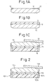
- an acrylic adhesive resinous material 12 of UV-curing type which has a modulus of elasticity after curing of about 10 MPa, is applied to the entire periphery of beveled portion of the side of a silicon wafer 10, on which chip circuits is formed, by ink jet printing, so as to have a width and a height of the order of 40 and 20 micrometers, respectively.
- a protective tape 14 of pressure sensitivity type is attached to the chip circuit-formed side of the wafer 10, during which the resinous material 12 at the beveled portion is spread to be leveled.
- the resinous material 12 is cured by irradiation with UV light having a main wavelength of 365 nanometers at a dose of 1200 mJ/cm 2 .
- the wafer 10, with the side having the protective tape 14 attached down, is then place on a wafer table 16, and the back side of the wafer 10 is roughly ground by a grinding wheel 18, at the conditions of 3 ⁇ m/sec wheel feed rate, 2400 rpm wheel rotational speed, and 200 rpm table rotational speed. Subsequently, finish grinding is carried out at the conditions of 0.5 ⁇ m/sec wheel feed rate, 2400 rpm wheel rotational speed, and 200 rpm table rotational speed. After the completion of grinding, the wafer is polished at the conditions of 150 g/cm 2 (14.7 kPa) pressure, 280 rpm buffing wheel rotational sped, and 240 rpm table rotational speed. The wafer 10 is then removed from the table 16, and the protective tape 14 is peeled off, to obtain a thinned silicon wafer of 10 micrometers thick free of peripheral cracks.
- the invention makes it possible to thin even a wafer having a small thickness without developing peripheral cracks, and can contribute to the improvement in productivity of chips manufactured from a wafer.
Landscapes
- Engineering & Computer Science (AREA)
- Chemical & Material Sciences (AREA)
- Ceramic Engineering (AREA)
- Inorganic Chemistry (AREA)
- Mechanical Engineering (AREA)
- Mechanical Treatment Of Semiconductor (AREA)
Applications Claiming Priority (2)
| Application Number | Priority Date | Filing Date | Title |
|---|---|---|---|
| JP2003148113A JP2004349649A (ja) | 2003-05-26 | 2003-05-26 | ウエハーの薄加工方法 |
| JP2003148113 | 2003-05-26 |
Publications (1)
| Publication Number | Publication Date |
|---|---|
| EP1501120A1 true EP1501120A1 (de) | 2005-01-26 |
Family
ID=33447638
Family Applications (1)
| Application Number | Title | Priority Date | Filing Date |
|---|---|---|---|
| EP04012241A Withdrawn EP1501120A1 (de) | 2003-05-26 | 2004-05-24 | Verfahren zum dünnschleifen eines Substrats |
Country Status (3)
| Country | Link |
|---|---|
| US (1) | US6958298B2 (de) |
| EP (1) | EP1501120A1 (de) |
| JP (1) | JP2004349649A (de) |
Families Citing this family (24)
| Publication number | Priority date | Publication date | Assignee | Title |
|---|---|---|---|---|
| JP3922255B2 (ja) * | 2003-06-30 | 2007-05-30 | ブラザー工業株式会社 | 固体撮像素子及びその製造方法、装着方法 |
| US20060162850A1 (en) * | 2005-01-24 | 2006-07-27 | Micron Technology, Inc. | Methods and apparatus for releasably attaching microfeature workpieces to support members |
| US8124455B2 (en) * | 2005-04-02 | 2012-02-28 | Stats Chippac Ltd. | Wafer strength reinforcement system for ultra thin wafer thinning |
| US7169248B1 (en) * | 2005-07-19 | 2007-01-30 | Micron Technology, Inc. | Methods for releasably attaching support members to microfeature workpieces and microfeature assemblies formed using such methods |
| US7786551B2 (en) * | 2005-09-16 | 2010-08-31 | Stats Chippac Ltd. | Integrated circuit system with wafer trimming |
| JP4395775B2 (ja) | 2005-10-05 | 2010-01-13 | ソニー株式会社 | 半導体装置及びその製造方法 |
| US7749349B2 (en) * | 2006-03-14 | 2010-07-06 | Micron Technology, Inc. | Methods and systems for releasably attaching support members to microfeature workpieces |
| JP5832060B2 (ja) * | 2008-02-18 | 2015-12-16 | デンカ株式会社 | 電子部品集合体の研削方法とこれを用いた電子部品集合体の分割方法 |
| JP5495647B2 (ja) * | 2009-07-17 | 2014-05-21 | 株式会社ディスコ | ウェーハの加工方法 |
| EP2671249A4 (de) | 2011-02-01 | 2015-10-07 | Henkel IP & Holding GmbH | Auf einem vorgeschnittenen wafer angebrachter unterfüllungsfilm |
| EP2671248A4 (de) * | 2011-02-01 | 2015-10-07 | Henkel Corp | Auf einem vorgeschnittenen wafer angebrachter unterfüllungsfilm auf einem dicing-tape |
| JP5841738B2 (ja) * | 2011-04-05 | 2016-01-13 | 株式会社ディスコ | ウェーハの研削方法 |
| JP2013008915A (ja) * | 2011-06-27 | 2013-01-10 | Toshiba Corp | 基板加工方法及び基板加工装置 |
| JP2013243223A (ja) * | 2012-05-18 | 2013-12-05 | Disco Abrasive Syst Ltd | ウエーハ保護部材 |
| DE112012006750B4 (de) * | 2012-07-30 | 2026-01-08 | Erich Thallner | Substratverbund, Verfahren und Vorrichtung zum Bonden von Substraten |
| JP6061557B2 (ja) * | 2012-08-01 | 2017-01-18 | 株式会社ミマキエンジニアリング | 部材付着式装飾方法 |
| EP2752871B1 (de) * | 2013-01-08 | 2015-09-16 | ams AG | Verfahren der Anwendung eines Trägers auf einen Vorrichtungswafer |
| JP5784658B2 (ja) * | 2013-02-28 | 2015-09-24 | 株式会社東芝 | 半導体装置の製造方法及び製造装置 |
| JP6197422B2 (ja) | 2013-07-11 | 2017-09-20 | 富士通セミコンダクター株式会社 | 半導体装置の製造方法および支持基板付きウェハ |
| US9716010B2 (en) * | 2013-11-12 | 2017-07-25 | Globalfoundries Inc. | Handle wafer |
| DE102015002542B4 (de) * | 2015-02-27 | 2023-07-20 | Disco Corporation | Waferteilungsverfahren |
| CN105931997B (zh) * | 2015-02-27 | 2019-02-05 | 胡迪群 | 暂时性复合式载板 |
| CN109877694B (zh) * | 2019-03-04 | 2023-08-08 | 天通日进精密技术有限公司 | 晶圆边缘抛光装置及晶圆边缘抛光方法 |
| CN116110801A (zh) * | 2021-11-11 | 2023-05-12 | 中芯国际集成电路制造(天津)有限公司 | 一种晶圆堆叠结构及其形成方法 |
Citations (8)
| Publication number | Priority date | Publication date | Assignee | Title |
|---|---|---|---|---|
| JPS55164623A (en) * | 1979-06-07 | 1980-12-22 | Toyo Ink Mfg Co Ltd | Preparation of plaster |
| JPH09115863A (ja) * | 1995-10-23 | 1997-05-02 | Oki Electric Ind Co Ltd | 表面保護テープ貼り付け方法およびその装置 |
| JPH1031142A (ja) * | 1996-07-16 | 1998-02-03 | Nikon Corp | 極薄厚板状の光学素子を備えている光学部品、極薄厚板状の光学素子の接合方法 |
| JPH11297719A (ja) * | 1998-04-07 | 1999-10-29 | Matsushita Electric Ind Co Ltd | 電子部品実装装置および電子部品実装方法 |
| EP0981156A2 (de) * | 1998-08-18 | 2000-02-23 | Lintec Corporation | Haftklebefolie zum Oberflächenschutz beim Schleifen der Rückseite eines Halbleiterplättchens und Verfahren zur Verwendung derselben |
| JP2000353682A (ja) * | 1999-06-11 | 2000-12-19 | Tokyo Seimitsu Co Ltd | 半導体保護テープの切断方法 |
| JP2002110601A (ja) | 2000-10-04 | 2002-04-12 | Naoetsu Electronics Co Ltd | ウエハのワックス塗布方法 |
| JP2002264008A (ja) | 2001-03-13 | 2002-09-18 | Naoetsu Electronics Co Ltd | ウエハ保持プレート及びウエハ吸着ホルダー |
Family Cites Families (9)
| Publication number | Priority date | Publication date | Assignee | Title |
|---|---|---|---|---|
| JPS61152358A (ja) * | 1984-12-24 | 1986-07-11 | Toshiba Corp | 半導体ウエハの研削方法 |
| JPS61292922A (ja) * | 1985-06-21 | 1986-12-23 | Hitachi Hokkai Semiconductor Ltd | 半導体装置の製造方法 |
| JPH06252109A (ja) * | 1993-02-26 | 1994-09-09 | Fujitsu Ltd | 半導体装置の製造方法 |
| JP3423245B2 (ja) * | 1999-04-09 | 2003-07-07 | 沖電気工業株式会社 | 半導体装置及びその実装方法 |
| US6338980B1 (en) * | 1999-08-13 | 2002-01-15 | Citizen Watch Co., Ltd. | Method for manufacturing chip-scale package and manufacturing IC chip |
| JP2001093867A (ja) | 1999-09-21 | 2001-04-06 | Rodel Nitta Kk | ウエハ外周部の保護部材及びウエハの研磨方法 |
| JP3282164B2 (ja) | 1999-12-27 | 2002-05-13 | 直江津電子工業株式会社 | ウエハ接着剤塗布方法 |
| JP2003147300A (ja) * | 2001-11-12 | 2003-05-21 | Lintec Corp | ウエハ裏面研削時の表面保護シートおよび半導体チップの製造方法 |
| CN1509495A (zh) * | 2002-03-14 | 2004-06-30 | ������������ʽ���� | 半导体晶片背面研磨方法 |
-
2003
- 2003-05-26 JP JP2003148113A patent/JP2004349649A/ja active Pending
-
2004
- 2004-05-24 EP EP04012241A patent/EP1501120A1/de not_active Withdrawn
- 2004-05-24 US US10/851,191 patent/US6958298B2/en not_active Expired - Fee Related
Patent Citations (8)
| Publication number | Priority date | Publication date | Assignee | Title |
|---|---|---|---|---|
| JPS55164623A (en) * | 1979-06-07 | 1980-12-22 | Toyo Ink Mfg Co Ltd | Preparation of plaster |
| JPH09115863A (ja) * | 1995-10-23 | 1997-05-02 | Oki Electric Ind Co Ltd | 表面保護テープ貼り付け方法およびその装置 |
| JPH1031142A (ja) * | 1996-07-16 | 1998-02-03 | Nikon Corp | 極薄厚板状の光学素子を備えている光学部品、極薄厚板状の光学素子の接合方法 |
| JPH11297719A (ja) * | 1998-04-07 | 1999-10-29 | Matsushita Electric Ind Co Ltd | 電子部品実装装置および電子部品実装方法 |
| EP0981156A2 (de) * | 1998-08-18 | 2000-02-23 | Lintec Corporation | Haftklebefolie zum Oberflächenschutz beim Schleifen der Rückseite eines Halbleiterplättchens und Verfahren zur Verwendung derselben |
| JP2000353682A (ja) * | 1999-06-11 | 2000-12-19 | Tokyo Seimitsu Co Ltd | 半導体保護テープの切断方法 |
| JP2002110601A (ja) | 2000-10-04 | 2002-04-12 | Naoetsu Electronics Co Ltd | ウエハのワックス塗布方法 |
| JP2002264008A (ja) | 2001-03-13 | 2002-09-18 | Naoetsu Electronics Co Ltd | ウエハ保持プレート及びウエハ吸着ホルダー |
Non-Patent Citations (5)
| Title |
|---|
| PATENT ABSTRACTS OF JAPAN vol. 005, no. 041 (C - 047) 18 March 1981 (1981-03-18) * |
| PATENT ABSTRACTS OF JAPAN vol. 1997, no. 09 30 September 1997 (1997-09-30) * |
| PATENT ABSTRACTS OF JAPAN vol. 1998, no. 06 30 April 1998 (1998-04-30) * |
| PATENT ABSTRACTS OF JAPAN vol. 2000, no. 01 31 January 2000 (2000-01-31) * |
| PATENT ABSTRACTS OF JAPAN vol. 2000, no. 15 6 April 2001 (2001-04-06) * |
Also Published As
| Publication number | Publication date |
|---|---|
| US6958298B2 (en) | 2005-10-25 |
| US20040242003A1 (en) | 2004-12-02 |
| JP2004349649A (ja) | 2004-12-09 |
Similar Documents
| Publication | Publication Date | Title |
|---|---|---|
| US6958298B2 (en) | Method for thinning wafer by grinding | |
| US8029335B2 (en) | Wafer processing method | |
| US6910403B1 (en) | Method for cutting semiconductor wafer protecting sheet | |
| TWI686854B (zh) | 晶圓的加工方法 | |
| KR102432506B1 (ko) | 웨이퍼 가공 방법 및 중간 부재 | |
| JP2001044144A (ja) | 半導体チップの製造プロセス | |
| KR102742368B1 (ko) | 피가공물의 가공 방법 | |
| JP4806282B2 (ja) | ウエーハの処理装置 | |
| KR20210052225A (ko) | 웨이퍼의 가공 방법 | |
| CN102848305B (zh) | 被加工物的磨削方法 | |
| CN105097637A (zh) | 支承板、支承板的形成方法和晶片的加工方法 | |
| CN107808898A (zh) | 晶片和晶片的加工方法 | |
| JP2012079910A (ja) | 板状物の加工方法 | |
| JP3216583B2 (ja) | 貼り合わせsoi基板の製造方法 | |
| JP2877997B2 (ja) | 半導体ウエハの処理方法 | |
| KR100816641B1 (ko) | 반도체 웨이퍼 가공방법 및 이것에 사용되는 지지기판 | |
| JP7191467B2 (ja) | 被加工物の研削方法 | |
| JP4681704B2 (ja) | 半導体ウェーハの分割方法 | |
| KR20110055977A (ko) | 반도체 패키지 제조용 장비 및 이를 이용한 반도체 패키지 제조방법 | |
| JP7313775B2 (ja) | ウェーハの加工方法 | |
| JP3982572B2 (ja) | 板状物保護テープ及び半導体ウェーハの研磨方法 | |
| KR20170016284A (ko) | 피가공물의 가공 방법 | |
| US12409527B2 (en) | Grinding method for circular plate-shaped workpiece | |
| US20220274224A1 (en) | Grinding method for workpiece | |
| JP7699451B2 (ja) | 加工方法 |
Legal Events
| Date | Code | Title | Description |
|---|---|---|---|
| PUAI | Public reference made under article 153(3) epc to a published international application that has entered the european phase |
Free format text: ORIGINAL CODE: 0009012 |
|
| AK | Designated contracting states |
Kind code of ref document: A1 Designated state(s): AT BE BG CH CY CZ DE DK EE ES FI FR GB GR HU IE IT LI LU MC NL PL PT RO SE SI SK TR |
|
| AX | Request for extension of the european patent |
Extension state: AL HR LT LV MK |
|
| 17P | Request for examination filed |
Effective date: 20041213 |
|
| AKX | Designation fees paid |
Designated state(s): DE |
|
| 17Q | First examination report despatched |
Effective date: 20101029 |
|
| RAP1 | Party data changed (applicant data changed or rights of an application transferred) |
Owner name: SHINKO ELECTRIC INDUSTRIES CO., LTD. |
|
| STAA | Information on the status of an ep patent application or granted ep patent |
Free format text: STATUS: THE APPLICATION IS DEEMED TO BE WITHDRAWN |
|
| 18D | Application deemed to be withdrawn |
Effective date: 20161201 |