EP1489609B1 - Procede de fabrication d'un support d'enregistrement d'informations optiques a couches multiples - Google Patents
Procede de fabrication d'un support d'enregistrement d'informations optiques a couches multiples Download PDFInfo
- Publication number
- EP1489609B1 EP1489609B1 EP03744978A EP03744978A EP1489609B1 EP 1489609 B1 EP1489609 B1 EP 1489609B1 EP 03744978 A EP03744978 A EP 03744978A EP 03744978 A EP03744978 A EP 03744978A EP 1489609 B1 EP1489609 B1 EP 1489609B1
- Authority
- EP
- European Patent Office
- Prior art keywords
- stamper
- layer
- signal recording
- optical information
- manufacturing
- Prior art date
- Legal status (The legal status is an assumption and is not a legal conclusion. Google has not performed a legal analysis and makes no representation as to the accuracy of the status listed.)
- Expired - Lifetime
Links
- 230000003287 optical effect Effects 0.000 title claims description 133
- 238000004519 manufacturing process Methods 0.000 title claims description 123
- 239000000758 substrate Substances 0.000 claims abstract description 218
- 238000000926 separation method Methods 0.000 claims abstract description 189
- 238000012546 transfer Methods 0.000 claims description 123
- 229910052751 metal Inorganic materials 0.000 claims description 108
- 239000002184 metal Substances 0.000 claims description 108
- 229920005989 resin Polymers 0.000 claims description 105
- 239000011347 resin Substances 0.000 claims description 105
- 239000000463 material Substances 0.000 claims description 77
- 239000004820 Pressure-sensitive adhesive Substances 0.000 claims description 43
- 230000005855 radiation Effects 0.000 claims description 42
- 238000000465 moulding Methods 0.000 claims description 35
- 239000004033 plastic Substances 0.000 claims description 23
- 229920003023 plastic Polymers 0.000 claims description 23
- 238000001746 injection moulding Methods 0.000 claims description 21
- 239000012212 insulator Substances 0.000 claims description 15
- 239000004417 polycarbonate Substances 0.000 claims description 15
- 229920000515 polycarbonate Polymers 0.000 claims description 15
- 239000000853 adhesive Substances 0.000 claims description 12
- 230000001070 adhesive effect Effects 0.000 claims description 12
- 229920000178 Acrylic resin Polymers 0.000 claims description 5
- 239000004925 Acrylic resin Substances 0.000 claims description 5
- 229920005672 polyolefin resin Polymers 0.000 claims description 5
- 238000007493 shaping process Methods 0.000 claims description 4
- 230000007246 mechanism Effects 0.000 claims description 2
- 230000001788 irregular Effects 0.000 abstract 1
- 239000010410 layer Substances 0.000 description 507
- 238000000034 method Methods 0.000 description 76
- 239000010408 film Substances 0.000 description 74
- 239000012790 adhesive layer Substances 0.000 description 49
- PXHVJJICTQNCMI-UHFFFAOYSA-N Nickel Chemical compound [Ni] PXHVJJICTQNCMI-UHFFFAOYSA-N 0.000 description 32
- 229910052759 nickel Inorganic materials 0.000 description 16
- 238000005259 measurement Methods 0.000 description 11
- 239000011521 glass Substances 0.000 description 9
- 238000001723 curing Methods 0.000 description 8
- 238000009826 distribution Methods 0.000 description 8
- 239000000498 cooling water Substances 0.000 description 7
- 238000004528 spin coating Methods 0.000 description 6
- 230000008859 change Effects 0.000 description 5
- 238000007796 conventional method Methods 0.000 description 5
- 230000001678 irradiating effect Effects 0.000 description 5
- 238000009987 spinning Methods 0.000 description 5
- 230000015572 biosynthetic process Effects 0.000 description 4
- 238000013007 heat curing Methods 0.000 description 4
- 229920002120 photoresistant polymer Polymers 0.000 description 4
- 238000004544 sputter deposition Methods 0.000 description 4
- 229910000763 AgInSbTe Inorganic materials 0.000 description 3
- 229910000618 GeSbTe Inorganic materials 0.000 description 3
- HEMHJVSKTPXQMS-UHFFFAOYSA-M Sodium hydroxide Chemical compound [OH-].[Na+] HEMHJVSKTPXQMS-UHFFFAOYSA-M 0.000 description 3
- NIXOWILDQLNWCW-UHFFFAOYSA-N acrylic acid group Chemical group C(C=C)(=O)O NIXOWILDQLNWCW-UHFFFAOYSA-N 0.000 description 3
- QSHDDOUJBYECFT-UHFFFAOYSA-N mercury Chemical compound [Hg] QSHDDOUJBYECFT-UHFFFAOYSA-N 0.000 description 3
- 229910052753 mercury Inorganic materials 0.000 description 3
- 229910001507 metal halide Inorganic materials 0.000 description 3
- 150000005309 metal halides Chemical class 0.000 description 3
- 239000000049 pigment Substances 0.000 description 3
- 229910052724 xenon Inorganic materials 0.000 description 3
- FHNFHKCVQCLJFQ-UHFFFAOYSA-N xenon atom Chemical compound [Xe] FHNFHKCVQCLJFQ-UHFFFAOYSA-N 0.000 description 3
- 230000000694 effects Effects 0.000 description 2
- 239000011344 liquid material Substances 0.000 description 2
- 238000003825 pressing Methods 0.000 description 2
- 239000010409 thin film Substances 0.000 description 2
- 238000007740 vapor deposition Methods 0.000 description 2
- 230000004075 alteration Effects 0.000 description 1
- 229910052782 aluminium Inorganic materials 0.000 description 1
- XAGFODPZIPBFFR-UHFFFAOYSA-N aluminium Chemical compound [Al] XAGFODPZIPBFFR-UHFFFAOYSA-N 0.000 description 1
- 239000007864 aqueous solution Substances 0.000 description 1
- 230000008901 benefit Effects 0.000 description 1
- KGBXLFKZBHKPEV-UHFFFAOYSA-N boric acid Chemical compound OB(O)O KGBXLFKZBHKPEV-UHFFFAOYSA-N 0.000 description 1
- 239000004327 boric acid Substances 0.000 description 1
- 239000011248 coating agent Substances 0.000 description 1
- 238000000576 coating method Methods 0.000 description 1
- 230000008602 contraction Effects 0.000 description 1
- 238000001816 cooling Methods 0.000 description 1
- 238000013036 cure process Methods 0.000 description 1
- 238000005516 engineering process Methods 0.000 description 1
- PCHJSUWPFVWCPO-UHFFFAOYSA-N gold Chemical compound [Au] PCHJSUWPFVWCPO-UHFFFAOYSA-N 0.000 description 1
- 239000010931 gold Substances 0.000 description 1
- 229910052737 gold Inorganic materials 0.000 description 1
- 239000004615 ingredient Substances 0.000 description 1
- KERTUBUCQCSNJU-UHFFFAOYSA-L nickel(2+);disulfamate Chemical compound [Ni+2].NS([O-])(=O)=O.NS([O-])(=O)=O KERTUBUCQCSNJU-UHFFFAOYSA-L 0.000 description 1
- 230000003647 oxidation Effects 0.000 description 1
- 238000007254 oxidation reaction Methods 0.000 description 1
- 230000035699 permeability Effects 0.000 description 1
- 238000004080 punching Methods 0.000 description 1
- 238000004904 shortening Methods 0.000 description 1
- 229910052710 silicon Inorganic materials 0.000 description 1
- 239000010703 silicon Substances 0.000 description 1
- 239000007787 solid Substances 0.000 description 1
- 238000003892 spreading Methods 0.000 description 1
- 230000007480 spreading Effects 0.000 description 1
- 238000010301 surface-oxidation reaction Methods 0.000 description 1
- 230000001131 transforming effect Effects 0.000 description 1
Images


Classifications
-
- G—PHYSICS
- G11—INFORMATION STORAGE
- G11B—INFORMATION STORAGE BASED ON RELATIVE MOVEMENT BETWEEN RECORD CARRIER AND TRANSDUCER
- G11B7/00—Recording or reproducing by optical means, e.g. recording using a thermal beam of optical radiation by modifying optical properties or the physical structure, reproducing using an optical beam at lower power by sensing optical properties; Record carriers therefor
- G11B7/24—Record carriers characterised by shape, structure or physical properties, or by the selection of the material
- G11B7/26—Apparatus or processes specially adapted for the manufacture of record carriers
- G11B7/263—Preparing and using a stamper, e.g. pressing or injection molding substrates
-
- G—PHYSICS
- G11—INFORMATION STORAGE
- G11B—INFORMATION STORAGE BASED ON RELATIVE MOVEMENT BETWEEN RECORD CARRIER AND TRANSDUCER
- G11B7/00—Recording or reproducing by optical means, e.g. recording using a thermal beam of optical radiation by modifying optical properties or the physical structure, reproducing using an optical beam at lower power by sensing optical properties; Record carriers therefor
- G11B7/24—Record carriers characterised by shape, structure or physical properties, or by the selection of the material
- G11B7/2403—Layers; Shape, structure or physical properties thereof
- G11B7/24035—Recording layers
- G11B7/24038—Multiple laminated recording layers
Definitions
- the present invention relates to a method of manufacturing a multilayer optical information recording medium which has n (n: 2 or more) signal recording layers with a separation layer inserted between the respective signal recording layers, one side of which is used to record or reproduce information.
- a DVD provided with two layers for reproduction on one side has a structure with two substrates, one having an information recording surface on which a translucent reflecting layer of gold or silicon, etc., is formed and the other having an information recording surface on which a conventional reflecting layer made of aluminum, etc., is formed and the two substrates are pasted together in such a way that these information recording surfaces come inside facing each other.
- a high density optical information recording medium having a violet laser light source (with a wavelength of approximately 400 nm), a lens of high NA and a 0.1 mm thick low-profile transparent cover layer on the recording/reproducing side.
- This high density optical information recording medium has a structure with signal guide grooves or pits formed on the surface of a thick signal substrate, a rewritable recording multilayer film formed thereon and a transparent cover layer further formed thereon.
- the separation layer lying between the signal recording layers of the multilayer optical information recording medium must be uniform.
- the separation layer influences of reflected light from the other layer during recording or reproduction become constant in the signal recording layers before and after the separation layer.
- the reflected light from the other signal recording layer fluctuates, this becomes a disturbance component of the reproduced signal and deteriorates S/N.
- the separation layer is uniform, disturbance from the other signal recording layer is constant, which stabilizes recording or reproduction and improves the quality of the reproduced signal.
- a stamper is used to transfer the separation layer between the substrate and stamper and the signal guide grooves or pits from the stamper onto the surface.
- EP 1 178 478 relates to a multilayer disc in which each of the plurality of layers exhibits sufficient properties of reading.
- the radial variation of the thickness of the resin layers between the recording layers, which is due to spin coating, is compensated by making the surface of the substrate facing the recording layer thicker at the outer periphery than near the inner periphery.
- a first invention of the present invention is a method of manufacturing a multilayer optical information recording medium having n (n is an integer not smaller than 2) signal recording layers and a separation layer between the respective signal recording layers, assuming that the kth (k is an integer not smaller than 2 and not greater than n) signal recording layer from the recording surface or reproducing surface is a kth signal recording layer, the substrate having said kth signal recording layer on its surface is a kth signal substrate, the stamper having guide grooves and/or pits of the (k-1) th signal recording layer is a (k-1)th stamper and the separation layer between the kth signal recording layer and said (k-1)th signal recording layer is the (k-1)th separation layer, said method of manufacturing the multilayer optical information recording medium comprising:
- the (k-1)th stamper and the kth signal substrate are shaped parallel to each other, and therefore the distance between the two becomes uniform and the thickness of the (k-1)th separation layer created also becomes uniform.
- a second invention of the present invention is the method of manufacturing the multilayer optical information recording medium according to the first invention of the present invention, wherein when said kth signal substrate is warped so as to wrap around said kth signal recording layer, in said signal recording layer forming step, said (k-1)th stamper is warped so as to wrap around the surface opposite to the surface with guide grooves and/or pits of said (k-1)th signal recording layer.
- the distance between the kth signal recording layer and the surface having the guide grooves or pits or the guide grooves and pits of the (k-1)th signal recording layer becomes substantially uniform without changing the warpage of the kth signal substrate, and therefore the thickness of the manufactured (k-1)th separation layer becomes uniform.
- a third invention of the present invention is the method of manufacturing the multilayer optical information recording medium according to the first invention of the present invention, wherein when said kth signal substrate is warped so as to wrap around the opposite surface of the kth signal recording layer, in said signal recording layer forming step, said (k-1)th stamper is warped so as to wrap around the surface with guide grooves and/or pits of said (k-1)th signal recording layer.
- the distance between the kth signal recording layer and the surface having the guide grooves or pits or the guide grooves and pits of the (k-1)th signal recording layer becomes substantially uniform without changing the warpage of the kth signal substrate, and therefore the thickness of the manufactured (k-1)th separation layer becomes uniform.
- a fourth invention of the present invention is the method of manufacturing the multilayer optical information recording medium according to the second or the third invention of the present invention, wherein in said signal recording layer forming step, the kth signal recording layer of said kth signal substrate and the surface with guide grooves and/or pits of said (k-1)th signal recording layer are shaped so as to have substantially the same radius of curvature.
- the distance between the kth signal recording layer and the surface having the guide grooves or pits or the guide grooves and pits of the (k-1)th signal recording layer becomes substantially uniform without changing the warpage of the kth signal substrate, and therefore the thickness of the manufactured (k-1)th separation layer becomes uniform.
- a fifth invention of the present invention is the method of manufacturing the multilayer optical information recording medium according to the first invention of the present invention, wherein said (k-1)th separation layer is radiation cure resin.
- a sixth invention of the present invention is the method of manufacturing the multilayer optical information recording medium according to the fifth invention of the present inveniton, wherein said radiation cure resin is UV cure resin.
- a seventh invention of the present invention is the method of manufacturing the multilayer optical information recording medium according to the first invention of the present invention, wherein said (k-1)th separation layer consists of a plurality of layers.
- the above described configuration it is possible to arrange materials of different characteristics in the thickness direction of the (k-1)th separation layer and stably peel them off, for example, using a material having good adhesiveness with the kth signal recording layer as the material contacting the kth signal recording layer of the (k-1)th separation layer and using a material which can be easily peeled away from the (k-1)th stamper as the material contacting the surface having the guide grooves or pits or the guide grooves and pits of the (k-1)th signal recording layer on the (k-1)th stamper of the (k-1)th separation layer.
- An eighth invention of the present invention is the method of manufacturing the multilayer optical information recording medium according to the seventh invention of the present invention, wherein when a layer of said plurality of (k-1)th separation layers whose guide grooves and/or pits are transferred from said (k-1)th stamper is used as a transfer layer, of a plurality of interfaces including interfaces of the respective layers constituting said (k-1)th separation layer which exists between said (k-1)th stamper and said kth signal recording layer, the interface between said transfer layer and said (k-1)th stamper becomes the interface which is most easily peeled off.
- a ninth invention of the present invention is the method of manufacturing the multilayer optical information recording medium according to the seventh invention of the present invention, wherein when the layer of the plurality of said (k-1)th separation layers whose guide grooves and/or pits are transferred from said (k-1)th stamper is regarded as a transfer layer, at least said transfer layer is a radiation cure material
- the radiation cure material is easily cured with irradiation with radiation rays, and therefore it is possible to reliably copy shapes of grooves or pits from the (k-1)th stamper.
- a tenth invention of the present invention is the method of manufacturing the multilayer optical information recording medium according to the ninth invention of the present invention, wherein said radiation cure material is UV cure resin.
- An eleventh invention of the present invention is the method of manufacturing the multilayer optical information recording medium according to the tenth invention of the present invention, wherein the viscosity of said UV cure resin is 1 to 1000 mPa ⁇ s.
- UV cure resin can sufficiently fit into grooves or pits of the (k-1)th stamper, and therefore it is possible to improve transfers of grooves or pits.
- a twelfth invention of the present invention is the method of manufacturing the multilayer optical information recording medium according to the seventh invention of the present invention, wherein when the layer of the plurality of said (k-1)th separation layers whose guide grooves and/or pits are transferred from said (k-1)th stamper is regarded as a transfer layer, at least one of said (k-1)th separation layers other than the transfer layer is a pressure-sensitive adhesive.
- a thirteenth invention of the present invention is the method of manufacturing the multilayer optical information recording medium according to the seventh invention of the present inveniton, wherein when the layer of the plurality of said (k-1)th separation layers whose guide grooves and/or pits are transferred from said (k-1)th stamper is regarded as a transfer layer, in said signal recording layer forming step, a radiation cure material which becomes said transfer layer is coated on the surface with guide grooves and/or pits of said (k-1)th stamper and cured, and pasted to said kth signal substrate on which said (k-1)th separation layers except said transfer layer are formed.
- a fourteenth invention of the present invention is the method of manufacturing the multilayer optical information recording medium according to the thirteenth invention of the present invention, wherein when said (k-1)th stamper coated with said transfer layer is pasted to said kth signal substrate on which said (k-1)th separation layers except said transfer layer are formed, the surface of said (k-1)th separation layer which contacts said transfer layer coated on said (k-1)th stamper is a radiation cure material.
- a fifteenth invention of the present invention is the method of manufacturing the multilayer optical information recording medium according to the seventh invention of the present inveniton, wherein when the layer of the plurality of said (k-1)th separation layers whose guide grooves and/or pits are transferred from said (k-1)th stamper is regarded as a transfer layer, in said signal recording layer forming step, a radiation cure material which becomes said transfer layer is placed between said (k-1)th stamper and said kth signal substrate on which said (k-1)th separation layers except said transfer layer are formed and then said radiation cure material is cured.
- the radiation-cured resin spreads uniformly through a capillary phenomenon and it is possible to further improve uniformity in the thickness of the separation layer. Furthermore, it is also possible to easily form a transfer layer through irradiation with radiation rays while keeping the uniformity.
- a sixteenth invention ofhte present invention is the method of manufacturing the multilayer optical information recording medium according to the fifteenth invention of the present inveniton, wherein in said signal recording layer forming step, the radiation cure material which becomes said transfer layer is applied to at least one of the surface on which said (k-1)th separation layers except said transfer layer of said kth signal substrate and the surface with guide grooves and/or pits of said (k-1)th stamper and then said kth signal substrate is superimposed on said (k-1)th stamper and said radiation cure material is cured.
- a radiation cure material is applied to the entire surface of the (k-1)th stamper or the kth signal substrate before the two are put together, and therefore it is possible to adhere the surface of the (k-1)th stamper to the surface of the kth signal substrate and unite the separation layer over the entire surface.
- a seventeenth invention of the present invention is the method of manufacturing the multilayer optical information recording medium according to the thirteenth invention of the present invention, wherein in said signal recording layer forming step, when said kth signal substrate and said (k-1)th stamper are arranged with said kth signal recording layer and the surface with guide grooves and/or pits of said (k-1)th signal recording layer facing each other, at least one of said kth signal substrate and said (k-1)th stamper is held in such a way that said (k-1)th stamper is shaped parallel to said kth signal substrate and then said radiation cure material is cured.
- the radiation cure material is cured by holding at least one of the two so that the shapes of the two are parallel to each other, and therefore it is not necessary to control the shapes of the kth signal substrate and the (k-1)th stamper and the margin of creation of the kth signal substrate and the (k-1)th stamper can be widened.
- An eighteenth invention of the present invention is the method of manufacturing the multilayer optical information recordingmedium according to the seventeenth invention of the present invention, wherein in said signal recording layer forming step, at least one of said kth signal substrate and said (k-1)th stamper is fixed onto a support base having a desired surface shape and then said radiation cure material is cured.
- the support member is used and the surface shape thereof is kept to a desired shape, it is possible to easily change the kth signal substrate or the (k-1)th stamper in a shape parallel to each other.
- a nineteenth invention of the present invention is the method of manufacturing the multilayer optical information recording medium according to the first invention of the present inveniton, wherein said (k-1)th stamper is made of plastic.
- the weight of the (k-1)th stamper is reduced and therefore the (k-1)th stamper can be easily handled and can also improve productivity.
- a twentieth invention of the present invention is the method of manufacturing the multilayer optical information recording medium according to the nineteenth invention of the present invention, wherein said plastic is transparent.
- the separation layer is a radiation cure material
- a twenty-first invention of the present invention is the method of manufacturing the multilayer optical information recording medium according to the twentieth invention of the present invention, wherein said (k-1)th stamper is any one of polycarbonate, olefin resin, acrylic resin or norbornen-based resin and is created according to an injection molding method using a metal master stamper.
- stampers can be created at a low cost and in bulk, which improves the capacity of volume production of multilayer optical information recording media.
- a twenty-second invention of the present invention is the method of manufacturing the multilayer optical information recording medium according to the twenty-first invention of the present invention, wherein in said signal recording layer forming step, when said kth signal substrate and said (k-1)th stamper are arranged with the kth signal recording layer and the surface with guide grooves and/or pits of said (k-1)th signal recording layer facing each other according to the conditions of the injection molding method in creating said (k-1)th stamper, said (k-1)th stamper is controlled so as to be shaped parallel to said kth signal substrate.
- the shape of the (k-1)th stamper can be accurately controlled through only injection molding conditions no matter what kind of warpage the kth signal substrate may have.
- a twenty-third invention of the present invention is the method of manufacturing the multilayer optical information recording medium according to the twenty-second invention of the present invention, wherein in said signal recording layer forming step, when said (k-1)th stamper is created according to the injection molding method in order to shape said (k-1)th stamper warped so as to wrap around the surface opposite to the surface with guide grooves and/or pits of said (k-1)th signal recording layer, the temperature of the other metal die mirrored surface is set higher than the temperature of said metal master stamper placed on one of the pair of molding metal dies.
- the surface of the (k-1) th stamper made of plastics formed by an injection molding method is contracted more because immediately after it is removed from the molding die, the temperature of the surface opposite to the surface including the guide grooves or pits or the guide grooves and pits is higher, and it is therefore possible to warp the surface so as to wrap around the surface opposite to the surface including the guide grooves or pits or the guide grooves and pits.
- a twenty-fourth invention of the present invention is the method of manufacturing the multilayer optical information recording medium according to the twenty-third invention of the present inveniton, wherein in said signal recording layer forming step, the temperature of the other metal die mirrored surface is set higher than the temperature of the metal die mirrored surface on which said metal master stamper of the pair of molding metal dies is placed.
- the surface of the (k-1)th stamper made of plastics formed by an injection molding method is contracted more because immediately after it is removed from the molding die, the temperature of the surface opposite to the surface including the guide grooves or pits or the guide grooves and pits is higher, and it is therefore possible to warp the surface so as to wrap around the surface opposite to the surface including the guide grooves or pits or the guide grooves and pits.
- a twenty-fifth invention of the present inevniton is the method of manufacturing the multilayer optical information recording medium according to the twenty-third invention of the present invention, wherein a heat insulator is placed on the back of the metal die mirrored surface opposite to the metal die mirrored surface on which said metal master stamper of the pair of molding metal dies is placed.
- the heat insulator on the back makes it difficult for heat to dissipate, and can thereby effectively keep the temperature high.
- a twenty-sixth invention of the present invention is the method of manufacturing the multilayer optical information recording medium according to the twenty-second invention of the present invention, wherein in said signal recording layer forming step, when said (k-1)th stamper is created according to the injection molding method in order to shape said (k-1)th stamper warped so as to wrap around the surface with guide grooves and/or pits of said (k-1)th signal recording layer, the temperature of said metal master stamper placed on the metal die mirrored surface of the pair of molding metal dies is set higher than the temperature of the other metal die mirrored surface.
- the surface of the (k-1)th stamper made of plastics formed by an injection molding method is more contracted because immediately after it is removed from the molding die, the temperature of the surface including the guide grooves or pits or the guide grooves and pits is higher than the temperature of the opposite surface, and it is therefore possible to warp the surface so as to wrap around the surface including the guide grooves or pits or the guide grooves and pits.
- a twenty-seventh invention of the present invention is the method of manufacturing the multilayer optical information recording medium according to the twenty-sixth invention of the present invention, wherein in said signal recording layer forming step, the temperature of the metal die mirrored surface on which said metal master stamper of the pair of molding metal dies is placed is set higher than the temperature of the other metal die mirrored surface.
- a twenty-eighth invention of the present invention is the method of manufacturing the multilayer optical information recording medium according to the twenty-sixth invention of the present invention, wherein a heat insulator is placed on at least one of the back of said metal master stamper on which the pair of molding metal dies are placed and the back of the metal die mirrored surface on which said metal master stamper is placed.
- This method can also inhibit the heat of high-temperature injected plastics from spreading over the mirrored surface of the metal die and thereby make the temperature of the metal master stamper relatively higher than the temperature of the mirrored surface of the other metal die.
- a twenty-ninth invention of the present invention is the method of manufacturing the multilayer optical information recording medium according to the first invention of the present invention, wherein said (k-1)th stamper is metal.
- metal since metal has a relatively high degree of hardness, it is possible to suppress damage or deformation which may occur to the (k-1)th stamper when the (k-1)th stamper is peeled off the kth signal substrate and thereby improve the productivity of the multilayer optical information recording medium.
- a thirtieth invention of the present invention is the method of manufacturing the multilayer optical information recording medium according to the twenty-ninth invention of the present invention, wherein in said signal recording layer forming step, when said (k-1)th stamper is created by electrocasting and said kth signal substrate and said (k-1)th stamper are arranged with said kth signal recording layer and the surface with guide grooves and/or pits of said (k-1)th signal recording layer facing each other under at least one electrocasting conditions of the pH value, temperature and current density of the electrocasting bath during electrocasting, said (k-1)th stamper is controlled so as to be shaped parallel to said kth signal substrate.
- a thirty-first invention of the present invention is the method of manufacturing the multilayer optical information recording medium according to the first invention of the present invention, further comprising a film forming step after said peeling step, of completing the (k-1)th signal recording layer by forming a recording multilayer film (hereinafter referred to as (k-1)th recording multilayer film) or a reflecting film on the guide grooves and/or pits of said transferred (k-1)th signal recording layer.
- a film forming step after said peeling step of completing the (k-1)th signal recording layer by forming a recording multilayer film (hereinafter referred to as (k-1)th recording multilayer film) or a reflecting film on the guide grooves and/or pits of said transferred (k-1)th signal recording layer.
- a thirty-second invention of the present invention is the method of manufacturing the multilayer optical information recording medium according to the first invention of the present invention, wherein a (k-1)th recording multilayer film or a reflecting film is formed on the guide grooves and/or pits of the (k-1)th signal recording layer on said (k-1)th stamper and in said peeling step, said (k-1)th stamper is peeled off the interface between said (k-1)th recording multilayer film and said (k-1)th stamper and said (k-1)th recording multilayer film or reflecting film is moved onto said (k-1)th separation layer.
- a thirty-third invention of the present invention is the method of manufacturing the multilayer optical information recording medium according to the first invention of the present invention, wherein a transparent cover layer is formed on the first signal recording layer.
- a thirty-fourth invention of the present invention is the method of manufacturing the multilayer optical information recording medium according to the thirty-third invention of the present inveniton, wherein a transparent substrate is adhered to the first signal recording layer with a transparent adhesive as said transparent cover layer.
- a thirty-fifth invention of the present invention is the method of manufacturing the multilayer optical information recording medium according to the thirty-third invention of the present invention, wherein said transparent cover layer is formed of a transparent radiation cure material.
- a thirty-sixth invention of the present invention is the method of manufacturing the multilayer optical information recording medium according to the thirty-third invention of the present invention, wherein at least part of said transparent cover layer is formed of a pressure-sensitive adhesive.
- a thirty-seventh invention of the present invention is the method of manufacturing the multilayer optical information recording medium according to the thirty-third invention of the present invention, wherein the thickness of the transparent cover layer formed on the first signal recording layer is 0.3 mm or less.
- the 38th embodiment is an apparatus of manufacturing a multilayer optical information recording medium comprising n (n is an integer not smaller than 2) signal recording layers and a separation layer between the respective signal recording layers, wherein when it is assumed that the kth (k is an integer not smaller than 2 and not greater than n) signal recording layer from the recording surface or reproducing surface is the kth signal recording layer, the substrate having the kth signal recording layer on its surface is the kth signal substrate, the stamper having guide grooves and/or pits of the (k-1)th signal recording layer is the (k-1)th stamper and the separation layer between the kth signal recording layer and the (k-1)th signal recording layer is the (k-1)th separation layer, the apparatus of manufacturing the multilayer optical information recording medium comprises:
- the method of manufacturing the multilayer optical information recording medium of the above described embodiment it is easy to maintain the (k-1)th stamper and the kth signal substrate in a shape parallel to each other, it is also possible to form a separation layer between the two and peel off the (k-1)th stamper and the kth signal substrate. In this way, it is possible to manufacture a multilayer optical information recording medium with the separation layer having a uniform thickness.
- the 39th embodiment is the apparatus of manufacturing the multilayer optical information recording medium according to the 38th embodiment, wherein the shape maintaining means comprises a mechanism which holds the (k-1)th stamper so that when the kth signal substrate is warped, the guide grooves and/or pits of the (k-1)th signal recording layer and the kth signal recording layer are parallel to each other according to the warpage of the kth signal substrate.
- the present invention may be the 39th embodiment.
- the guide grooves or pits or the guide grooves and pits of the (k-1)th signal recording layer are parallel to the kth signal recording layer according to the warpage of the kth signal substrate, it is possible to keep uniform the thickness of the (k-1)th separation layer formed between the two.
- the 40th embodiment is the apparatus of manufacturing the multilayer optical information recording medium according to the 39th embodiment, wherein the shape maintaining means is table-shaped and has the surface shape that contacts the (k-1)th stamper so that the guide grooves and/or pits of the (k-1)th signal recording layer are parallel to the kth signal recording layer.
- the present invention may be the 40th embodiment.
- the 41st embodiment is the apparatus of manufacturing the multilayer optical information recording medium according to the 38th embodiment, wherein the shape maintaining means supports the surface of at least one of the (k-1)th stamper and the kth signal substrate for which the (k-1)th separation layer is not formed by "vacuum suction".
- the present invention may also be the 41st embodiment.
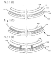
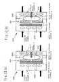
- Figure 1 shows an embodiment of a method of manufacturing a multilayer optical information recording medium according to the present invention.
- Figure 1 is a schematic view of a step of forming a (k-1)th separation layer 107 between a kth signal recording layer 100 and a (k-1)th signal recording layer of a disk type multilayer optical information recording medium having n (n: 2 or more) signal recording layers and a separation layer between the respective signal recording layers recording and reproducing information to/from one side.
- the kth signal recording layer 100 is the kth (k: 2 or above and n or below) signal recording layer from the recording/reproduction surface and a substrate having the kth signal recording layer 100 on the surface is a kth signal substrate 103.
- the stamper having guide grooves and pits 105 of the (k-1)th signal recording layer is a (k-1)th stamper 106.
- the step of forming a (k-1)th separation layer 107 of this embodiment is an example of the step of forming a signal recording layer of the present invention.
- the method of manufacturing the multilayer optical information recording medium of Embodiment 1 is intended to manufacture a high density optical information recording medium having a low-profile recording/reproducing side transparent cover layer of 0.3 mm or less and 2 ⁇ m or above in thickness using a violet laser light source (wavelength of approximately 400 nm) and a high NA lens to improve the surface recording density per one layer.
- the methods of manufacturing multilayer optical information recording media of embodiments other than Embodiment 1 are also intended to manufacture a high density optical information recording medium similar to that of Embodiment 1. It goes without saying that it is possible to apply the method of manufacturing the multilayer optical information recording medium of this embodiment to any media other than such a high density optical information recording medium.
- Both the kth signal substrate 103 and the (k-1)th stamper 106 in Figure 1 are disk-shaped and have a central hole in the center.
- the kth signal substrate 103 is designed to have a warped shape making allowances for warpage that can occur in other steps following the step of forming the (k-1)th separation layer 107 such as the step of forming a signal recording layer or a step of forming a transparent cover layer on the first signal recording layer.
- the kth signal substrate 103 is generally naturally warped due to stress caused in the step of forming the kth recording multilayer film of the kth signal recording layer 100, the step of forming the (k+1)th to nth separation layers and the step of forming the (k+1)th to nth recording multilayer films, etc.
- This Embodiment 1 shows the kth signal substrate 103 warped so as to wrap around the kth signal recording layer 100 as an example.
- the kth signal substrate 103 is prepared as shown in Figure 1(1) .
- the kth signal substrate 103 has a total of (n-k-1) signal recording layers from the (k+1)th signal recording layer 101 up to the nth signal recording layer 102.
- the signal recording layer consists of guide grooves for guiding recording light and reproducing light to record data in and reproduce data from the multilayer optical information recording medium, pits indicating address information, phase variation films such as GeSbTe and AgInSbTe, recording films represented by magnetic films and pigment films and recording multilayer film made of a dielectric film such as ZnS sandwiching them or reflecting film.
- the multilayer optical information recording medium of this embodiment is not limited to the one made up of only guide grooves in which video/audio data is written after manufacturing but can also be the one made up of pits in which video/audio data is written during manufacturing or the one with pits formed inside or outside the guide grooves.
- the (k-1)th stamper 106 having guide grooves and pits 105 of the (k-1)th signal recording layer on its surface is alsoprepared.
- the (k-1) th stamper 106 has been created by measuring the surface shape of one or a plurality of the kth signal substrates 103 which have been created currently or in the past as in the case of warpage measuring means 1401 which will be shown in Figure 14 of Embodiment 5 which will be described later and based on the measurement result, transforming the surface having guide grooves and pits 105 of the (k-1) th signal recording layer of the (k-1)th stamper 106 into the shape corresponding to the surface shape of the kth signal substrate 103. That is, the (k-1)th stamper 106 has been formed so as to conform to the shape of the kth signal substrate 103.
- the surface shape of the kth signal substrate 103 may be measured by measuring the surface shape of the kth signal substrate 103 manufactured first in the morning the day before when the plant operates and determining the shape of the (k-1)th stamper 106 based on the measurement result. Furthermore, it is also possible to measure the shape of the kth signal substrates 103 one by one every time the kth signal substrate 103 is manufactured and determine the shape of the (k-1)th stamper 106 based on the measurement result. Furthermore, it is also possible to determine the shape of the (k-1)th stamper 106 using the measurement result of the shape surface of the kth signal substrate 103 for each lot.
- the (k-1)th stamper 106 and the kth signal substrate 103 come to have shapes parallel to each other as shown in the figure. That is, the guide grooves and pits 105 of the (k-1)th signal recording layer and the kth signal recording layer 100 are arranged parallel to each other and the distance between the two becomes uniform in the radial direction and within the surface. That is, the kth signal recording layer 100 of the kth signal substrate 103 and the surface having guide grooves and/or pits 105 of the (k-1)th signal recording layer are shaped so as to have substantially the same curvature radius.
- a substrate having a plurality of signal recording layers as in the case of the kth signal substrate 103 is warped due to stress of the films such as recording multilayer films and reflecting films.
- the (k-1)th stamper 106 of this embodiment is shaped so as to be parallel to the already warped kth signal substrate 103 and guide grooves and pits 105 of the (k-1)th signal recording layer and the kth signal recording layer 100 are arranged so as to face each other.
- the (k-1)th separation layer 107 is formed between the guide grooves and pits 105 of the (k-1)th signal recording layer and the kth signal recording layer 100.
- the distance between the guide grooves and pits 105 of the (k-1)th signal recording layer and the kth signal recording layer 100 is uniform in the radial direction and within the surface, and therefore the thickness of the (k-1)th separation layer 107 becomes uniform.
- the (k-1)th separation layer 107 need not always be made of one material but may also be made up of a plurality of layers made of different materials.
- the layer contacting the guide grooves and pits 105 of the (k-1)th signal recording layer of the (k-1)th separation layer 107 is used as a transfer layer, if a liquid material having a curing characteristic is used as a transfer layer, it is easily fitted into the guide grooves and pits 105 of the (k-1) th signal recording layer and it is possible to improve transferability. In this case, the transfer layer is cured and the (k-1)th separation layer 107 is completed.
- peeling is performed from the interface between the guide grooves and pits 108 of the transferred (k-1)th signal recording layer on the (k-1)th separation layer 107 and the (k-1)th stamper 106.
- Such peeling can provide the (k-1)th signal substrate.
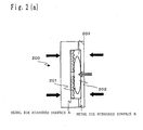
- Figure 2 shows a step of forming the (k-1)th stamper.
- plastic is used as the material of the (k-1)th stamper.
- Plastic is light, has an excellent operability and is convenient because it can be easily created in bulk using an injection molding method. It also has an advantage that a desired shape (warpage) can be provided by controlling molding conditions.
- polycarbonate is used as the material of the (k-1)th stamper. In addition to polycarbonate, olefin resin, acrylic resin and norbornen-based resin, etc., can also be used.
- a master stamper 201 is placed on a metal die mirrored surface A of a pair of molding metal dies 200 and polycarbonate 202 melted at 380°C is molded and charged into the molding metal die 200.
- the master stamper 201 is made of, for example, a material whose principal ingredient is metal such as nickel.
- a cavity 203 formed between the master stamper 201 of the molding metal die 200 and the metal die mirrored surface B is predetermined to have a desired thickness of the (k-1)th stamper.
- the thickness of the cavity 203 for forming the (k-1)th stamper of approximately 1.1 mm in thickness is 1.1 mm.
- the metal die mirrored surface A and the metal die mirrored surface B of the molding metal die 200 are set to their respective temperatures.
- the temperatures of the metal die mirrored surfaces A and B are set to 115°C and 125°C respectively so that (temperatures of metal die mirrored surface A) ⁇ (temperatures of metal die mirrored surface B). These temperatures allow the polycarbonate 202 melted at 380°C to be cooled and calcified.
- a mold pressing force of 20 to 30 t is applied to the molding metal die 200. The mold pressing force causes the melted polycarbonate to fit into the guide grooves and pits formed in the master stamper 201 and to transfer them.
- the (k-1)th stamper 204 is removed from the molding metal die 200.
- (temperature of metal die mirrored surface A) ⁇ (temperature of metal die mirrored surface B) the temperature of the surface 205 on which guide grooves and pits of the (k-1)th stamper 204 are formed is lower than the temperature of the surface 206 on the opposite side. Therefore, the amount of contraction when the temperature is lowered to a room temperature is greater on the surface 206 on the opposite side and as a result, the (k-1)th stamper 204 acquires a shape wrapping around the surface 206 on the opposite side.
- the (k-1)th stamper 106 shown in Figure 1(1) is created in this way.
- Figure 3 shows a step of forming the (k-1)th separation layer.
- the (k-1)th separation layer is made of two materials and a case where both the outside diameter of the kth signal substrate and the outside diameter of the (k-1)th stamper are 120 mm will be explained using an example.
- a (k-1)th stamper 300 is placed on a table 305 with the surface provided with guide grooves and pits of the (k-1)th stamper facing upward.
- the (k-1)th stamper 300 can be created using the method shown in Figure 2 .
- the (k-1)th stamper 300 set is fixed onto the table 305 using a method such as vacuum suction.
- the surface shape of the table 305 is preferably shaped with the same curvature as that of the (k-1)th stamper as shown in the figure. This is because the shape of the (k-1)th stamper 300 itself is controlled in the step shown in Figure 2 .
- transfer layer UV cure resin 301 With transfer layer UV cure resin 301 dribbled onto the surface with the guide grooves and pits of the (k-1) th stamper, the table 305 is turned to throw off extra transfer layer UV cure resin and a layer of the transfer layer UV cure resin of a uniform thickness is obtained.
- the UV cure resin acrylic resin which radically reacts with irradiation of UV rays is preferable.
- acrylic UV cure resin with a viscosity of 200 MPa ⁇ s which can be easily peeled from the polycarbonate (k-1)th stamper 300 is used.
- UV cure resin with a viscosity of 1 to 1000 MPa ⁇ s can well fit into the projections and depressions of guide grooves and pits on the stamper. Through spinning at a speed of 4000 rpm for 5 seconds, a transfer layer of approximately 8 ⁇ m in thickness was obtained.
- UV rays are irradiated using a UV lamp 302.
- a UV lamp 302. a metal halide lamp, high pressure mercury lamp or xenon lamp, etc., is preferably used. Irradiation with UV rays cures the transfer layer UV cure resin 301 and forms a transfer layer 303.
- the (k-1)th stamper 300 on which the transfer layer 303 is formed is pasted to the kth signal substrate 306.
- the kth signal substrate 306 not only the guide grooves and pits of the kth signal recording layer and kth recording multilayer film are formed, but also the (k+1)th to nth signal recording layers (not shown) are included.
- an adhesive layer UV cure resin 307 which becomes an adhesive is dribbled onto the kth signal recording layer and the transfer layer 303 of the (k-1)th stamper 300 is placed so as to contact the adhesive layer UV cure resin 307.
- the table 309 is turned as shown in the figure to throw off extra adhesive layer UV cure resin.
- the table was turned at 5000 rpm for 8 seconds.
- acrylic UV cure resin of 600 mPa ⁇ s with high strength of adhesion to the kth recording multilayer film and transfer layer 303 was used.
- UV rays are irradiated from the UV lamp 302 to cure the adhesive layer UV cure resin 307.
- a metal halide lamp, high pressure mercury lamp or xenon lamp, etc. can be used as in the case of above described Figure 3 (b) .
- the (k-1)th stamper 300 has transparency such as polycarbonate, and therefore can allow UV rays to penetrate to some extent to cure the adhesive layer UV cure resin 307.
- the average thickness of the adhesive layer 308 is 22 ⁇ m and the transfer layer 303 and adhesive layer 308 which have been united by the cure becomes a (k-1)th separation layer 310.
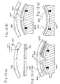
- the thickness of the (k-1)th separation layer 310 was as shown in Figure 4 (a) .
- the thickness of the (k-1)th separation layer in the radial direction was 27 to 31 ⁇ m , which is a variation of 4 ⁇ m, which canbe considered uniform.
- Figure 4(b) shows a thickness variation of the (k-1)th stamper in the radial direction of the (k-1)th separation layer created using a conventional method. The thickness tends to increase toward the inside radius and has a large
- the thickness variation of the (k-1)th separation layer in the radial direction is 4 ⁇ m, which can be considered uniform, but it is possible to maintain the performance of a high density optical information recording medium if the variation is within 6 ⁇ m.
- Figure 5 shows how the (k-1)th separation layer is created when the (k-1)th stamper is created into a flat shape using the injection molding method as in the conventional method. It is substantially the same as the steps shown in Figure 3 except that the shape of the (k-1)th stamper 500 is flat.
- Figures 5(a) and 5 (b) show the step of forming a transfer layer 503
- Figures 5(c) and 5(d) show the step of forming an adhesive layer 508 and completing a (k-1)th separation layer 510. Since the shape of the (k-1)th stamper 500 is flat, it is natural that a table 505 be flat.
- the distance between the surface with guide grooves and pits of the (k-1)th stamper 500 and the kth signal recording layer of the kth signal substrate 306 increases toward the inside radius.
- the thickness of an adhesive layer 508 increases toward the inside radius as shown in Figure 5 (d) and as a result, the thickness of the (k-1)th separation layer 510 consisting of the adhesive layer 508 and transfer layer 503 also increases toward the inside radius.
- FIG. 3 has described the step of forming the (k-1)th separation layer, but steps shown in (A) to (C) below are also effective instead.
- Figure 3 (c) has described the case where with the kth signal substrate 306 fixed on the table 309 by means of vacuum suction, the adhesive layer UV cure resin 307 which becomes an adhesive is dribbled onto the kth signal recording layer and the transfer layer 303 of the (k-1)th stamper 300 is placed from above so as to contact the adhesive layer UV cure resin 307, then the table 309 is turned to throw off extra adhesive layer UV cure resin, but the method is not limited to this.
- Figure 6 shows a peeling step.
- the (k-1)th stamper 300 and the kth signal substrate 306 bonded together in the step shown in Figure 3 are fixed on a peeling table 600.
- the means of fixing can be vacuum suction in Figure 6(a) , but other means include, for example, a machine which holds the circumferential end surface of the kth signal substrate 306.
- a lug 610 is inserted into the central hole of the (k-1)th stamper 300 and the kth signal substrate 306 and the lug 610 is inserted into the interface between the transfer layer 303 which is part of the (k-1)th separation layer 310 and the (k-1)th stamper 300.
- the end of the lug 610 is sharp, the lug 610 can be easily inserted as a wedge into the interface between the transfer layer 303 and the (k-1)th stamper 300.
- pressurized air 615 is introduced from the center of the peeling table 600 into the area between the transfer layer 303 and the (k-1)th stamper 300.
- the (k-1)th stamper 300 is pulled up using the handling means 612. Pulling it up using the handling means 612 facilitates the peeling.
- the (k-1)th stamper 300 is peeled off as shown in Figure 6(d) .
- the (k-1)th recording multilayer film is formed on the guide grooves and pits of the (k-1)th signal recording layer transferred on the (k-1)th separation layer.
- the method of forming the (k-1)th recording multilayer film varies depending on the material, phase variation films such as GeSbTe and AgInSbTe, recording films such as magnetic films, dielectric films such as ZnS sandwiching them and metal reflecting film, etc., are formed by sputtering and vapor deposition. Furthermore, in the case of the pigment film, spin coating is used. It is only after the (k-1)th recordingmultilayer film is formed that the (k-1)th signal recording layer is completed. By repeating the steps shown in Figure 2 , Figure 3 and Figure 6 and formation of the recording multilayer film on the (k-1)th signal recording layer, a first signal substrate having n signal recording layers is created.
- a method shown in Figure 11 can also be used. This is effective when it is difficult to form the (k-1)th recording multilayer film on the guide grooves and pits of the (k-1)th signal recording layer transferred onto the (k-1)th separation layer.
- the (k-1)th recording multilayer film 1101 is formed on the (k-1)th stamper 300 beforehand using a target 1100 and using a sputtering method.
- a target 1100 is shown, but since the (k-1)th recording multilayer film 1101 is actually made of a plurality of materials, a plurality of targets are necessary.
- the (k-1)th separation layer 310 consisting of the transfer layer 303 and adhesive layer 308 is formed.
- the (k-1)th separation layer 310 is fixed on the peeling table 600 and as shown in Figure 11 (c) , the (k-1)th stamper 300 is peeled using the handling means 612.
- the procedure up to the peeling is the same as that shown in Figure 6 , and therefore it is omitted here.
- the (k-1)th stamper 300 is peeled off the (k-1)th recording multilayer film 1101 and the (k-1)th recording multilayer film 1101 is moved onto the (k-1)th separation layer 310.
- Guide grooves and pits are formed on the transfer layer 303 and at the same time the (k-1)th recording multilayer film 1101 is also formed.
- Using this step makes it possible to form the (k-1)th separation layer onto the kth signal substrate and at the same time form the (k-1)th recording multilayer film and there is an expectation of shortening of a tact time.
- Figure 7 shows an example of a step of creating a transparent cover layer on the first signal recording layer.
- the thickness of the transparent cover layer is 100 ⁇ m.
- a film 700 of 90 ⁇ m in thickness is bonded on the table 720 using an adhesive layer 730 of 10 ⁇ m in thickness by spin coating to form the cover layer.
- the material of the film 700 polycarbonate, olefin resin or norbornen-based resin, etc., can be used.
- the adhesive layer 730 UV cure resin, radiation-cured material such as heat-cured resin can be used.
- Figure 7(b) shows a method of bonding the film 700 using a pressure-sensitive adhesive 740 and forming a cover layer.
- the thickness of the pressure-sensitive adhesive 740 is 20 to 30 ⁇ m and the thickness of the film 700 obtained by subtracting the thickness of the pressure-sensitive adhesive 740 from 100 ⁇ m is used.
- the bonding method used is, for example, a method of overlapping the film 700 with the pressure-sensitive adhesive 740 in the chamber 745 with a reduced pressure shown in Figure 7(b) . After overlapping them, the film surface is pressed with a high-pressure compressed air to secure the bonding.
- a method of pasting using a roller in the atmosphere or under a reduced pressure may also be used.
- Figure 7 (c) shows a method whereby a cover material 750 is applied by spin coating without using any film. Optimizing the condition of supplying the cover material 750 and the condition of spin rotation makes it possible to form a uniform transparent cover layer of 100 ⁇ m in thickness. Using the above described methods shown in Figure 7 , the transparent cover layer is formed and a multilayer optical information recording medium is completed.
- the plastic (k-1)th stamper of 1.1 mm in thickness is used, but any plastic stamper that has a thickness of at least 0.5 mm is acceptable. If the stamper has a thickness of 0.5 mm or more, since it also has rigidity, its shape can be easily controlled according to the molding condition using the injection molding method and it can be easily handled, which is suited to improving productivity.
- Embodiment 1 has described the case where the (k-1)th separation layer is made of two materials, but it is also applicable to a case where the (k-1)th separation layer is made of three or more materials. Furthermore, Embodiment 1 has been described using UV cure resin, but it is also possible to use a radiation cure material including a heat cure material.
- Embodiment 2 of the method of manufacturing a multilayer optical information recording medium according to the present invention will be explained.
- Figure 8 shows a case with warpage opposite to that in Embodiment 1, that is, a case where the kth signal substrate is warped so as to wrap around the surface opposite to the kth signal recording layer.
- both the kth signal substrate and the (k-1)th stamper in Figure 8 have a disk shape and have a central hole in the center.
- the kth signal substrate 803 is provided with not only the kth signal recording layer 800 on the surface of the kth separation layer 810 but also a total of (n-k-1) signal recording layers from the (k+1)th signal recording layer 801 to the nth signal recording layer 802.
- the signal recording layer consists of guide grooves for guiding recording light or reproducing light when information is recorded in or reproduced from the multilayer optical information recording medium or pits indicating address information, phase variation film such as GeSbTe or AgInSbTe, recording film represented by magnetic film and pigment film and recording multilayer film made of dielectric films such as ZnS sandwiching them or reflecting film.
- the (k-1)th stamper 806 having the guide grooves and pits 805 of the (k-1)th signal recording layer on the surface is also prepared.
- the (k-1)th stamper 806 is formed by measuring the surface shapes of one or a plurality of kth signal substrates 803 manufactured currently or in the past as in the case of warpage measuring means 1401 which will be shown in Figure 14 of Embodiment 5 as will be described later, shaping the surface with guide grooves and/or pits 805 of the (k-1)th signal recording layer of the (k-1)th stamper 806 to conform to the surface shape of the kth signal substrate 803 based on the measurement result. That is, the (k-1)th stamper 806 is in a shape parallel to the kth signal substrate 803.
- the (k-1)th stamper 806 and the kth signal substrate 803 are shaped parallel to each other as shown in the figure and the (k-1)th stamper 806 is warped so as to wrap around the guide grooves and pits 805 of the (k-1)th signal recording layer. That is, the guide grooves and pits 805 of the (k-1)th signal recording layer and the kth signal recording layer 800 are shaped parallel to each other and the distance is uniform in the radial direction and within the surface. That is, the kth signal recording layer 800 of the kth signal substrate 803 and the surface with the guide grooves and/or pits 805 of the (k-1)th signal recording layer are shaped so as to have substantially the same radius of curvature.
- a (k-1)th separation layer 807 is formed between the guide grooves and pits 805 of the (k-1)th signal recording layer and the kth signal recording layer 800.
- the (k-1)th stamper side of the (k-1)th separation layer 807 needs to be formed so as to fit into the guide grooves and pits 805 of the (k-1)th signal recording layer.
- the thickness of the (k-1)th separation layer is uniform.
- the (k-1)th separation layer 807 need not only be made of one material but also may be made up of a plurality of layers made of different materials.
- the layer of the (k-1)th separation layer 807 which contacts the guide grooves and pits 805 of the (k-1)th signal recording layer is regarded as a transfer layer, if a liquid material with a curing characteristic is used as the transfer layer, it is easily fitted into the guide grooves and pits 805 of the (k-1)th signal recording layer and transferability can be improved. In this case, the transfer layer is cured and the (k-1)th separation layer 807 is completed.
- the (k-1)th stamper can be created using the injection molding method shown in Figure 2 .
- the (k-1)th stamper 204 is shaped so as to wrap around the surface 205 on which the guide grooves and pits are formed after it is removed from the molding metal die 200.
- Figure 9 shows an example of forming the (k-1)th separation layer of 30 ⁇ m in thickness using a pressure-sensitive adhesive and a transfer layer.
- Figure 9 shows a method of using a pressure-sensitive adhesive as part of the (k-1)th separation layer.
- the pressure-sensitive adhesive has excellent thickness accuracy because it has a semi-solid film-like shape.
- having a very high viscosity it is difficult for the pressure-sensitive adhesive to transfer the guide grooves and pits of the (k-1)th stamper.
- This formation method uses a transfer layer with a low viscosity separately.
- a kth signal substrate 900 and a pressure-sensitive adhesive 901 of 25 ⁇ m in thickness are put in a chamber 905 and the chamber 905 is vacuum-sealed.
- the degree of vacuum for example, a range of 1 to 100 hPa is appropriate.
- the pressure-sensitive adhesive 901 is superimposed on the surface of the kth signal recording layer of the kth signal substrate 900.
- the pressure-sensitive adhesive 901 has a central hole having a diameter of D1. D1 is greater than the diameter of the central hole D0 of the kth signal substrate. After the superimposition, the kth signal substrate and the pressure-sensitive adhesive are taken out into the atmosphere and the pressure-sensitive adhesive may be pressed under a high-pressure compressed air to secure the adhesion.
- the (k-1)th stamper 902 is fixed onto a table 904 as shown in Figure 9(b) , a transfer layer UV cure resin 903 is coated over the surface with guide grooves and pits of the (k-1)th signal recording layer.
- a transfer layer UV cure resin 903 is coated over the surface with guide grooves and pits of the (k-1)th signal recording layer.
- the transfer layer UV cure resin 903 acrylic resin which radically reacts with irradiation with UV rays is preferable as in the case of Embodiment 1.
- Acrylic UV cure resin with a viscosity of 20OMPa ⁇ s which can be easily peeled off the plastic (e.g., polycarbonate, olefin resin, etc.) (k-1)th stamper 902 is used.
- the transfer layer having a viscosity of 1 to 1000 MPa ⁇ s can well fit into projections and depressions of guide grooves and pits on the stamper. Furthermore, through spinning at a speed of 4000 rpm for 5 seconds, a transfer layer of approximately 8 ⁇ m in thickness was obtained. Furthermore, the inside diameter of the coated transfer layer UV cure resin 903 is D2 which is smaller than diameter D0 of the central hole of the (k-1)th stamper 902.
- the transfer layer UV cure resin 903 Since the transfer layer UV cure resin 903 has a low viscosity, it spread when superimposed and a total average thickness of the transfer layer UV cure resin 903 and pressure-sensitive adhesive 901 became 30 ⁇ m. After the superimposition, it is also possible to take out the kth signal substrate and the (k-1)th stamper into the atmosphere, crush bubbles produced when the kth signal substrate and the (k-1)th stamper are pressed against each other with a high-pressure compressed air or secure the adhesion.
- the uncured transfer layer UV cure resin 903 is cured by UV rays using a UV lamp 910.
- a (k-1)th separation layer 909 which consists of the pressure-sensitive adhesive 901 and transfer layer UV cure resin 903 is formed. Since UV rays penetrate to a certain degree if the (k-1)th stamper 902 is transparent, the transfer layer UV cure resin 903 can be well cured.
- the UV lamp a metal halide lamp, high pressure mercury lamp or xenon lamp, etc., can be used.
- the pressure-sensitive adhesive needs to have strength of adhesion to the kth signal recording layer and cured UV resin for transfer layer.
- the transfer UV cure resin be easily peeled from the (k-1)th stamper after the cure.
- the transfer layer UV cure resin 903 is applied to the (k-1)th stamper 902, but it is also possible to apply the transfer layer UV cure resin 903 to the pressure-sensitive adhesive 901 superimposed on the kth signal substrate 900. Furthermore, in Figure 9 , the pressure-sensitive adhesive 901 is superimposed on the kth signal substrate 900, but instead of this, it is also possible to apply the transfer layer UV cure resin 903 to the (k-1)th stamper 902 and then superimpose the pressure-sensitive adhesive 901 on the (k-1)th stamper 902 to which the transfer layer UV cure resin 903 is applied and then paste the kth signal substrate 900 to the (k-1)th stamper 902 .
- Figure 10(a) shows a thickness distribution of the (k-1)th separation layer 909 formed using the methods in Figure 8 and Figure 9 .
- Figure 10(b) shows a case where the (k-1)th separation layer is formed using the conventional flat (k-1)th stamper 500 as shown in Figure 5 according to the method in Figure 9 .
- the distance between the kth signal substrate and the (k-1)th stamper is small at the inside radius and large at the outside radius, and therefore the thickness of the (k-1)th separation layer tends to increase from the inside radius to the outside radius and a distribution of 6 ⁇ m between 27 and 33 ⁇ m is produced.
- Figure 8 and Figure 9 are effective for uniformity in the thickness of the (k-1)th separation layer.
- Embodiment 2 it is also possible to create the (k-1)th separation layer of a uniform thickness using the adhesive layer UV cure resin shown in Embodiment 1 according to the method shown in Figure 3 instead of the pressure-sensitive adhesive.
- the kth signal substrate is warped so as to wrap around the kth signal recording layer as in the case of Embodiment 1, it is also possible to apply the pressure-sensitive adhesive shown in Figure 9 .
- the plastic (k-1)th stamper of 1.1 mm in thickness was used, but any plastic stamper that has a thickness of at least 0.5 mm is acceptable. If the stamper has a thickness of 0.5 mm or more, since it also has rigidity, its shape can be easily controlled according to the molding condition using the injection molding method and it can be easily handled, which is suited to improving productivity.
- Embodiment 2 has described the case where the (k-1)th separation layer is made of two materials, but it is also applicable to a case where the (k-1)th separation layer is made of three or more materials. Furthermore, Embodiment 2 has been described using UV cure resin, but it is also possible to use a radiation cure material including a heat cure material.
- Figure 12 is a schematic view of a molding metal die provided with a heat insulator. This is intended to warp the (k-1)th stamper so as to wrap around the surface opposite to the surface on which guide grooves and pits are provided.
- FIG 12 (a) shows a case where a heat insulator 1200 is provided between a master stamper 201 and a metal die mirrored surface A. Cooling water flows through a cooling water channel A and a cooling water channel B to cool melted polycarbonate 202 introduced inside a cavity 203 of a molding metal die 200.
- the metal die mirrored surface B side is cooled according to the temperature of the cooling water that flows through the cooling water channel B, while for the master stamper 201 side, the temperature of the melted polycarbonate 202 is hardly cooled and therefore the master stamper 201 is warped more than the (k-1)th stamper molded with the molding metal die shown in Figure 2 .
- Cooling water can be flown through the cooling water channel A at a temperature necessary and enough to prevent the heat insulator 1200 from being broken by heat.
- Figure 12(b) shows a molding metal die with a heat insulator 1203 incorporated behind the metal die mirrored surface A. With this configuration, it is also possible to achieve the same effect.
- thermoelectric insulator not only on one side of the metal die mirrored surface of the above described pair of molding metal dies but also on both metal die mirrored surfaces.
- the plastic (k-1)th stamper of 1.1 mm in thickness is used, but any plastic stamper that has a thickness of at least 0.5 mm is acceptable. If the stamper has a thickness of 0.5 mm or more, since it also has rigidity, its shape can be easily controlled according to the molding condition using the injection molding method and it can be easily handled, which is suited to improving productivity.
- Embodiment 4 will describe the method of creating a metal (k-1)th stamper. Since metal has a relatively high degree of hardness, it is possible to suppress damage or deformation which may occur to the (k-1)th stamper when the (k-1)th stamper is peeled off the kth signal substrate and is therefore effective. Projections and depressions of guide grooves and pits must be switched round between the master stamper 201 and the (k-1)th stamper also shown in Figure 2 and Figure 12 . Therefore, it is possible to create a metal (k-1)th stamper using the master stamper 201.
- a master stamper is generally created using a glass master original disk having a shape whose projections and depressions are reverse to the guide grooves and pits on the master stamper.
- the surface of the glass master original disk is provided with projections and depressions which are guide grooves and pits formed on its glass surface using a photoresist.
- a photoresist is applied uniformly to the surface of a glass plate and the photoresist is exposed to condensed laser with UV to far-ultraviolet wavelengths and further electronic rays into the shapes of guide grooves and pits.
- the exposed photoresist area is removed in a developing step and projections and depressions such as guide grooves and pits are formed on the glass master original disk.
- a nickel thin film is formed on the surface of guide grooves and pits of the glass master original disk by means of vapor deposition or sputtering and nickel is deposited by electrocasting using the nickel thin film as an electrode.
- nickel is deposited to a thickness of 0.3 mm and a nickel plate is created on the surface of the glass master original disk.
- a master stamper having projections and depressions (guide grooves and pits) which are reversed projections and depressions (guide grooves and pits) on the glass master original disk is formed on the nickel plate.
- the master stamper is immersed in an aqueous solution of sodium hydroxide and used as an anode with a current of 20 A flowing for 60 seconds. In this way, an oxide film with the surface with projections and depressions of the master stamper subjected to oxidation treatment is formed.
- the entire master stamper is immersed in an electrocasting bath and this is used as a negative electrode to perform electrocasting.
- An electrocasting bath of nickel sulfamate (concentration: 550 g/L) and boric acid (concentration: 31 g/L) is used.
- the pH value, temperature and current density during electrocasting of the electrocasting bath are adjusted as required.
- Nickel is formed to a thickness of 0.3 mm on a master stamper by electrocasting and a 0.3 mm nickel (k-1)th stamper is obtained.
- + in the warpage direction means that the (k-1)th stamper is warped opposite to the surface with projections and depressions of the (k-1)th stamper
- - in the warpage direction means that the (k-1)th stamper is warped according to the surface with projections and depressions of the (k-1)th stamper.
- the magnitude of warpage is indicated with an angle formed by a tangential line of the (k-1)th stamper with respect to the radial direction of the (k-1)th stamper.
- the current density changes between + warpage and - warpage with 20 amperes/dm ⁇ 2 as the border.
- warpage is + when the temperature of the electrocasting bath is lower than 45°C
- warpage is - when the temperature of the electrocasting bath is higher than 45°C.
- pH of the electrocasting bath in Figure 13(c) warpage reaches a minimum with pH 4.5, that is, the (k-1)th stamper becomes flat and warpage is + as it goes away from the minimum value.
- the (k-1)th stamper when the (k-1)th stamper is created through electrocasting, if electrocasting is performed by controlling at least one of current density during electrocasting, temperature of the electrocasting bath and pH value, it is possible to control warpage of the (k-1)th stamper. With these parameters, it is possible to create the (k-1)th stamper in a shape parallel to the kth signal substrate.
- the metal (k-1)th stamper created in the above steps it is possible to form a separation layer in a space with the kth signal substrate using the method shown in Figure 3 and Figure 9 .
- the metal (k-1)th stamper is opaque and has no UV permeability, and therefore it is necessary to use radiation rays such as far-infrared rays for curing using a radiation-cured material such as a heat cure material instead of the adhesive layer UV cure resin 307 or transfer layer UV cure resin 903.
- a pressure-sensitive adhesive can also be used instead of the adhesive layer UV cure resin 307.
- nickel is used as metal in Embodiment 4, but any other metal can be used as the material if it allows at least electrocasting.
- the manufacturing apparatus comprises shape maintaining means of arranging the kth signal substrate and the (k-1)th stamper in such a way that the kth signal recording layer and the surface with guide grooves and pits of the (k-1)th signal recording layer facing each other and maintaining the shape so that the (k-1)th stamper and the kth signal substrate are shaped parallel to each other, separation layer forming means of, when at least one of the (k-1)th stamper and the kth signal substrate is maintained by the shape maintaining means in a shape parallel to each other, forming the (k-1)th separation layer between the kth signal recording layer and the guide grooves and pits of the (k-1)th signal recording layer and peeling means of peeling the (k-1)th stamper from the interface between the (k-1)th separation layer and the (k-1)th stamper.
- Figure 14 and Figure 15 show examples of the shape maintaining means and the separation layer forming means.
- the separation layer forming means of this embodiment is an example of the signal recording layer forming means of the present invention.
- Figure 14 is an example of a case where the shape maintaining means is an arm.
- a flat (k-1)th stamper 500 is used with a transfer layer 503 formed on the guide grooves and pits shown in Figure 14 (a) .
- the transfer layer is formed using the method shown in Figures 5 (a) and 5 (b) .
- a kth signal substrate 306 is warped so as to wrap around the kth signal recording layer.
- Warpage measuring means 1401 calculates an angle of inclination of the kth signal recording layer on the kth signal substrate by causing measuring light 1402 to enter the kth signal recording layer on the kth signal substrate 306 and detecting the position of the reflected measuring light 1402.
- the shape maintaining arm 1400 maintains the surface opposite to the surface on which the transfer layer 503 of the (k-1)th stamper 500 is formed to the inside radius side and the outside radius side. At this time, the shape maintaining arm 1400 maintains the (k-1)th stamper 500 in a warped position so that guide grooves and pits of the (k-1)th signal recording layer are kept parallel to the kth signal recording layer according to the angle of inclination of the kth signal recording layer obtained from the warpage measuring means 1401.
- the warpage measuring means 1401 measures the surface shape of the kth signal recording layer of one or a plurality of the kth signal substrates 306 manufactured currently or in the past and the shape maintaining arm 1400 shapes the surface with the guide grooves and/or pits of the (k-1)th signal recording layer of the (k-1)th stamper 500 in such a way as to conform to the surface shape of the kth signal substrate 306 based on the measurement result. That is, the shape maintaining arm 1400 forms the (k-1)th stamper 500 in a shape parallel to the shape of the kth signal substrate 306 based on the measurement result.
- the shape of the kth signal substrate 306 may be measured by measuring the shape of the kth signal substrate 306 manufactured first in the morning the day before when the plant operates and determining the shape of the (k-1)th stamper 500 based on the measurement result. Furthermore, it is also possible to measure the shape of the kth signal substrates 306 one by one every time the kth signal substrate 306 is manufactured and determine the shape of the (k-1)th stamper 500 based on the measurement result. Furthermore, it is also possible to determine the shape of the (k-1)th stamper 500 using the measurement result of the shape of the kth signal substrate 306 for each lot.
- the member which holds the stamper of the shape maintaining arm 1400 has driving means such as an air cylinder, stepping motor and actuator, etc. Furthermore, the holding method includes vacuum suction and a mechanical holding method such as a lug in the case of the outside radius side.
- the table 309 which holds the kth signal substrate 306 is turned.
- the shape maintaining arm 1400 also rotates in synchronization with the table 309 while holding the (k-1) th stamper 500.
- the adhesive layer UV cure resin 307 spreads in the radial direction and forms a uniform adhesive layer between the (k-1)th stamper 500 and the kth signal substrate 306.
- the adhesive layer is cured by UV rays and peeling is performed as shown in Figure 6 .
- the lug 610 in Figure 6 and the handling means 612 constitute part of the peeling means.
- the shape maintaining arm 1400 holds the (k-1)th stamper 500 as shown in Figure 14(d) .
- Figure 15 shows a case where the shape maintaining means has a table shape.
- a flat (k-1)th stamper 500 with a transfer layer 503 formed on guide grooves and pits shown in Figure 15(a) is used.
- the transfer layer is formed using the method shown in Figures 5(a) and 5(b) .
- the kth signal substrate 306 is warped so as to wrap around the kth signal recording layer.
- the warpage measuring means 1401 calculates an angle of inclination of the kth signal recording layer on the kth signal substrate by causing measuring light 1402 to enter the kth signal recording layer on the kth signal substrate 306 and detecting the position of the reflected measuring light 1402.
- the shape maintaining table 1500 holds the surface of the (k-1) th stamper 500 on which the transfer layer 503 is formed. At this time, the shape maintaining table 1500 holds the (k-1)th stamper 500 warped so that guide grooves and pits of the (k-1)th signal recording layer are kept parallel to the kth signal recording layer according to the angle of inclination of the kth signal recording layer obtained from the warpage measuring means 1401.
- a convex shape maintaining table 1500 which shapes the (k-1)th stamper 500 so as to wrap around the surface opposite to the surface provided with guide grooves and pits as shown in Figure 15 (b)
- a concave shape maintaining table 1501 which shapes the (k-1)th stamper 500 so as to wrap around the surface provided with guide grooves and pits as shown in Figure 15(d) is selected and the (k-1)th stamper 500 is held.
- the holding method includes vacuum suction and a mechanical holding method such as a lug in the case of the outside radius side.
- the table is turned. Through this rotation, the adhesive layer UV cure resin 307 spreads in the radial direction and forms a uniform adhesive layer between the (k-1)th stamper 500 and the kth signal substrate 306. With the shape of the (k-1)th stamper maintained by the shape maintaining table 1500, the adhesive layer is cured by UV rays and peeling is performed as shown in Figure 6 .
- the lug 610 in Figure 6 and the handling means 612 constitute part of the peeling means.
- Figure 15(c) has shown the method of inserting the nozzle 1403 between the kth signal substrate 306 and the (k-1)th stamper 500 and dribbling the adhesive layer UV cure resin 307, but it is also possible to dribble the adhesive layer UV cure resin 307 directly onto the (k-1)th stamper using the nozzle and then drop the kth signal substrate on top of it. These two types of dribbling method can also be used in the steps in Figure 3(c) .
- Embodiment 5 has described the method of forming the (k-1)th separation layer from two types of material of the adhesive layer using the transfer layer and UV cure resin, but Embodiment 5 is also applicable when the (k-1)th separation layer other than the transfer layer exists on the kth signal substrate.
- this embodiment is applicable to a method of dribbling a material which becomes a transfer layer on a pressure-sensitive adhesive which exists on the kth signal substrate.
- Embodiment 5 has described the method of changing the shape of the (k-1)th stamper by the shape maintaining means according to the shape (warpage) of the kth signal substrate having a plurality of signal recording layers, but it is also possible to change the shape of kth signal substrate. Changing the shape generally distorts a plurality of signal recording layers, and therefore it is preferable to change the shape of the (k-1)th stamper.
- Embodiment 5 has used the plastic (k-1)th stamper of 1.1 mm in thickness, but any plastic stamper that has a thickness of at least 0.5 mm is acceptable. If the stamper has a thickness of 0.5 mm or more, since it also has rigidity, its shape can be easily controlled according to the molding condition using the injection molding method and it can be easily handled, which is suited to improving productivity. Furthermore, the metal stamper shown in Embodiment 4 can also be used instead of the plastic (k-1)th stamper.
- Embodiment 5 has described the case where the plastic (k-1)th separation layer is made of two materials, but this embodiment is also applicable to a case where the (k-1)th separation layer is made of three or more materials. Furthermore, Embodiment 5 has been described using UV cure resin, but it is also possible to use a radiation cure material including a heat cure material.
- the method of manufacturing the multilayer optical information recording medium of the present invention forms the (k-1)th separation layer by maintaining the kth signal recording layer of the kth signal substrate and the surface provided with guide grooves or pits or guide grooves and pits of the (k-1)th stamper in a shape parallel to each other, and can thereby keep constant the distance between the kth signal recording layer of the kth signal substrate and the surface provided with guide grooves or pits or guide grooves and pits of the (k-1)th stamper and keep uniform the thickness of the (k-1)th separation layer formed.
Landscapes
- Engineering & Computer Science (AREA)
- Manufacturing & Machinery (AREA)
- Manufacturing Optical Record Carriers (AREA)
- Optical Record Carriers And Manufacture Thereof (AREA)
Abstract
Claims (41)
- Procédé de fabrication d'un support d'enregistrement d'information optique multicouche ayant n couches (n étant un entier supérieur ou égal à 2) d'enregistrement de signal (100) et une couche de séparation (107) entre les couches d'enregistrement de signal respectives, en admettant que la ke couche (k étant un entier supérieur ou égal à 2 et inférieur ou égal à n) d'enregistrement de signal de la surface d'enregistrement ou de reproduction est une ke couche d'enregistrement de signal, que le substrat (103) ayant ladite ke couche d'enregistrement de signal sur sa surface est un ke substrat de signal, que la matrice de pressage (106) ayant des rainures et/ou cavités de guidage (108) de la (k-1)e couche d'enregistrement de signal est une (k-1)e matrice de pressage et que la couche de séparation entre la ke couche d'enregistrement de signal et ladite (k-1)e couche d'enregistrement de signal est la (k-1)e couche de séparation, ledit procédé de fabrication du support d'enregistrement d'information optique multicouche comprenant :une étape de mesure de formes de surface d'un ou d'une pluralité desdits ke substrats de signal fabriqués actuellement ou antérieurement ;une étape de formage d'une couche d'enregistrement de signal pour la mise en forme de la surface comportant des rainures et/ou cavités de guidage de ladite (k-1)e couche d'enregistrement de signal de ladite (k-1)e matrice de pressage de manière à correspondre à la forme de surface dudit ke substrat de signal et pour la formation de ladite (k-1)e couche d'enregistrement de signal en utilisant la (k-1)e matrice de pressage ; etune étape de pelage de ladite (k-1)e matrice de pressage de l'interface entre ladite (k-1)e couche de séparation et ladite (k-1)e matrice de pressage,dans laquelle au moins une desdites n couches d'enregistrement de signal est créée au cours de ladite étape de formage d'une couche d'enregistrement de signal.
- Procédé de fabrication du support d'enregistrement d'information optique multicouche selon la revendication 1, dans lequel lorsque ledit ke substrat de signal est déformé de manière à envelopper ladite ke couche d'enregistrement de signal, au cours de ladite étape de formage d'une couche d'enregistrement de signal, ladite (k-1)e matrice de pressage est déformée de manière à envelopper la surface opposée à la surface comportant des rainures et/ou cavités de guidage de ladite (k-1)e couche d'enregistrement de signal.
- Procédé de fabrication du support d'enregistrement d'information optique multicouche selon la revendication 1, dans lequel lorsque ledit ke substrat de signal est déformé de manière à envelopper la surface opposée de la ke couche d'enregistrement de signal, au cours de ladite étape de formage d'une couche d'enregistrement de signal, ladite (k-1)e matrice de pressage est déformée de manière à envelopper la surface comportant des rainures et/ou cavités de guidage de ladite (k-1)e couche d'enregistrement de signal.
- Procédé de fabrication du support d'enregistrement d'information optique multicouche selon la revendication 2 ou 3, dans lequel au cours de ladite étape de formage d'une
couche d'enregistrement de signal, la ke couche d'enregistrement de signal dudit ke substrat de signal et la surface comportant des rainures et/ou cavités de guidage de ladite (k-1)e couche d'enregistrement de signal sont formées de manière à présenter un rayon de courbure sensiblement identique. - Procédé de fabrication du support d'enregistrement d'information optique multicouche selon la revendication 1, dans lequel ladite (k-1)e couche de séparation est constituée d'une résine polymérisant sous rayonnement.
- Procédé de fabrication du support d'enregistrement d'information optique multicouche selon la revendication 5, dans lequel ladite résine polymérisant sous rayonnement est une résine polymérisant sous rayonnement UV.
- Procédé de fabrication du support d'enregistrement d'information optique multicouche selon la revendication 1, dans lequel ladite (k-1)e couche de séparation consiste en une pluralité de couches.
- Procédé de fabrication du support d'enregistrement d'information optique multicouche selon la revendication 7, dans lequel lorsqu'une couche de ladite pluralité de (k-1)e couches de séparation dont les rainures et/ou cavités de guidage sont transférées de ladite (k-1)e matrice de pressage est utilisée comme couche de transfert d'une pluralité d'interfaces comprenant des interfaces des couches respectives constituant ladite (k-1)e couche de séparation qui existe entre ladite (k-1)e matrice de pressage et ladite ke couche d'enregistrement de signal,
l'interface entre ladite couche de transfert et ladite (k-1)e matrice de pressage devient l'interface la plus facile à décoller. - Procédé de fabrication du support d'enregistrement d'information optique multicouche selon la revendication 7, dans lequel lorsque la couche de la pluralité desdites (k-1)e couches de séparation dont les rainures et/ou cavités de guidage sont transférées de ladite (k-1)e matrice de pressage est considérée comme une couche de transfert, au moins ladite couche de transfert est constituée d'un matériau polymérisant sous rayonnement.
- Procédé de fabrication du support d'enregistrement d'information optique multicouche selon la revendication 9, dans lequel ledit matériau polymérisant sous rayonnement est une résine polymérisant sous rayonnement UV.
- Procédé de fabrication du support d'enregistrement d'information optique multicouche selon la revendication 10, dans lequel la viscosité de ladite résine polymérisant sous rayonnement UV est de 1 à 1000 mPa.s.
- Procédé de fabrication du support d'enregistrement d'information optique multicouche selon la revendication 7, dans lequel, lorsque la couche de la pluralité desdites (k-1)e couches de séparation dont les rainures et/ou cavités de guidage sont transférées de ladite (k-1)e matrice de pressage est considérée comme une couche de transfert, au moins une desdites (k-1)e couches de séparation autre que la couche de transfert est un adhésif sensible à la pression.
- Procédé de fabrication du support d'enregistrement d'information optique multicouche selon la revendication 7, dans lequel, lorsque la couche de la pluralité desdites (k-1)e couches de séparation dont les rainures et/ou cavités de guidage sont transférées de ladite (k-1)e matrice de pressage est considérée comme une couche de transfert, au cours de ladite étape de formage d'une couche d'enregistrement de signal, une matériau polymérisant sous rayonnement qui devient ladite couche de transfert est revêtue sur la surface comportant des rainures et/ou cavités de guidage de ladite (k-1)e matrice de pressage, polymérisée et collée sur ledit ke substrat de signal sur lequel lesdites (k-1)e couches de séparation exceptée ladite couche de transfert sont formées.
- Procédé de fabrication du support d'enregistrement d'information optique multicouche selon la revendication 13, dans lequel, lorsque ladite (k-1)e matrice de pressage revêtue de ladite couche de transfert est collée audit ke substrat de signal sur lequel lesdites (k-1)e couches de séparation exceptée ladite couche de transfert sont formées, la surface de ladite (k-1)e couche de séparation qui entre en contact avec ladite couche de transfert revêtue sur ladite (k-1)e matrice de pressage est constituée d'un matériau polymérisant sous rayonnement.
- Procédé de fabrication du support d'enregistrement d'information optique multicouche selon la revendication 7, dans lequel, lorsque la couche de la pluralité desdites (k-1)e couches de séparation dont les rainures et/ou cavités de guidage sont transférées de ladite (k-1)e matrice de pressage est considérée comme une couche de transfert, au
cours de ladite étape de formage d'une couche d'enregistrement de signal, un matériau polymérisant sous rayonnement qui devient ladite couche de transfert est placé entre ladite (k-1)e matrice de pressage et ledit ke substrat de signal sur lequel lesdites (k-1)e couches de séparation exceptée ladite couche de transfert sont formées, et ledit matériau polymérisant sous rayonnement est ensuite polymérisé. - Procédé de fabrication du support d'enregistrement d'information optique multicouche selon la revendication 15, dans lequel, au cours de ladite étape de formage d'une couche d'enregistrement de signal, le matériau polymérisant sous rayonnement qui devient ladite couche de transfert est appliqué sur la surface sur laquelle lesdites (k-1)e couches de séparation exceptée ladite couche de transfert dudit ke substrat de signal et/ou sur la surface comportant des rainures et/ou cavités de guidage de ladite (k-1)e matrice de pressage, et ledit ke substrat de signal est ensuite superposé sur ladite (k-1)e matrice de pressage et ledit matériau polymérisant sous rayonnement est polymérisé.
- Procédé de fabrication du support d'enregistrement d'information optique multicouche selon la revendication 13, dans lequel, au cours de ladite étape de formage d'une couche d'enregistrement de signal, lorsque ledit ke substrat de signal et ladite (k-1)e matrice de pressage sont agencés avec ladite ke couche d'enregistrement de signal et la surface comportant des rainures et/ou cavités de guidage de ladite (k-1)e couche d'enregistrement de signal face à face, au moins un parmi ledit ke substrat de signal et ladite (k-1)e matrice de pressage est maintenu de
telle manière que ladite (k-1)e matrice de pressage est formée parallèlement audit ke substrat de signal, et ledit matériau polymérisant sous rayonnement est ensuite polymérisé. - Procédé de fabrication du support d'enregistrement d'information optique multicouche selon la revendication 17, dans lequel, au cours de ladite étape de formage d'une couche d'enregistrement de signal, ledit ke substrat de signal et/ou ladite (k-1)e matrice de pressage est fixé sur une base de support ayant une forme de surface désirée, et ledit matériau polymérisant sous rayonnement est ensuite polymérisé.
- Procédé de fabrication du support d'enregistrement d'information optique multicouche selon la revendication 1, dans lequel ladite (k-1)e matrice de pressage est réalisée en plastique.
- Procédé de fabrication du support d'enregistrement d'information optique multicouche selon la revendication 19, dans lequel ledit plastique est transparent.
- Procédé de fabrication du support d'enregistrement d'information optique multicouche selon la revendication 20, dans lequel ladite (k-1)e matrice de pressage est réalisée en polycarbonate, en résine polyoléfine, en résine acrylique ou en résine à base de norbornène et est créée selon un procédé de moulage par injection utilisant une matrice de pressage mère métallique.
- Procédé de fabrication du support d'enregistrement d'information optique multicouche selon la revendication 21, dans lequel, au cours de ladite étape de formage d'une couche d'enregistrement de signal, lorsque ledit ke substrat de signal et ladite (k-1)e matrice de pressage sont agencées avec la ke couche d'enregistrement de signal et la surface comportant des rainures et/ou cavités de guidage de ladite (k-1)e couche d'enregistrement de signal face à face, selon les conditions du procédé de moulage par injection en créant ladite (k-1)e matrice de pressage, ladite (k-1)e matrice de pressage est contrôlée de manière à être formée parallèlement audit ke substrat de signal.
- Procédé de fabrication du support d'enregistrement d'information optique multicouche selon la revendication 22, dans lequel, au cours de ladite étape de formage d'une couche d'enregistrement de signal, lorsque ladite (k-1)e matrice de pressage est créée selon le procédé de moulage par injection de manière à déformer ladite (k-1)e matrice de pressage pour envelopper la surface opposée à la surface avec des rainures et/ou cavités de guidage de ladite (k-1)e couche d'enregistrement de signal, la température de l'autre surface de matrice métallique réfléchie en miroir est réglée pour qu'elle soit supérieure à la température de ladite matrice de pressage mère métallique placée sur une des matrices métalliques de moulage de la paire.
- Procédé de fabrication du support d'enregistrement d'information optique multicouche selon la revendication 23, dans lequel, au cours de ladite étape de formage d'une couche d'enregistrement de signal, la température de l'autre surface de matrice métallique réfléchie en miroir est réglée pour qu'elle soit supérieure à la température de
la surface de matrice métallique réfléchie en miroir sur laquelle ladite matrice de pressage mère métallique de la paire de matrices métalliques de moulage est placée. - Procédé de fabrication du support d'enregistrement d'information optique multicouche selon la revendication 23, dans lequel un isolant thermique est placé au dos de la surface de matrice métallique réfléchie en miroir opposée à la surface de matrice métallique réfléchie en miroir sur laquelle ladite matrice de pressage mère métallique de la paire de matrices métalliques de moulage est placée.
- Procédé de fabrication du support d'enregistrement d'information optique multicouche selon la revendication 22, dans lequel, au cours de ladite étape de formage d'une couche d'enregistrement de signal, lorsque ladite (k-1)e matrice de pressage est créée selon le procédé de moulage par injection de manière à déformer ladite (k-1)e matrice de pressage pour envelopper la surface avec des rainures et/ou cavités de guidage de ladite (k-1)e couche d'enregistrement de signal, la température de ladite matrice de pressage mère métallique placée sur la surface de matrice métallique réfléchie en miroir de la paire de matrices métalliques de moulage est réglée pour qu'elle soit supérieure à la température de l'autre surface de matrice métallique réfléchie en miroir.
- Procédé de fabrication du support d'enregistrement d'information optique multicouche selon la revendication 26, dans lequel, au cours de ladite étape de formage d'une couche d'enregistrement de signal, la température de la surface de matrice métallique réfléchie en miroir sur
laquelle ladite matrice de pressage mère métallique de la paire de matrices métalliques de moulage est placée est réglée pour qu'elle soit supérieure à la température de l'autre surface de matrice métallique réfléchie en miroir. - Procédé de fabrication du support d'enregistrement d'information optique multicouche selon la revendication 26, dans lequel un isolant thermique est placé au dos de ladite matrice de pressage mère métallique sur laquelle la paire de matrices métalliques de moulage sont placées et/ou au dos de la surface de matrice métallique réfléchie en miroir sur laquelle ladite matrice de pressage mère métallique est placée.
- Procédé de fabrication du support d'enregistrement d'information optique multicouche selon la revendication 1, dans lequel ladite (k-1)e matrice de pressage est métallique.
- Procédé de fabrication du support d'enregistrement d'information optique multicouche selon la revendication 29, dans lequel, au cours de ladite étape de formage d'une couche d'enregistrement de signal, lorsque ladite (k-1)e matrice de pressage est créée par électromoulage et ledit ke substrat de signal et ladite (k-1)e matrice de pressage sont agencés avec ladite ke couche d'enregistrement de signal et la surface comportant des rainures et/ou cavités de guidage de ladite (k-1)e couche d'enregistrement de signal face à face, sous au moins une des conditions d'électromoulage de valeur de pH, température ou densité de courant du bain d'électromoulage pendant l'électromoulage, ladite (k-1)e matrice de pressage est contrôlée de manière à être formée parallèlement audit ke substrat de signal.
- Procédé de fabrication du support d'enregistrement d'information optique multicouche selon la revendication 1, comprenant en outre une étape de formation d'un film après ladite étape de pelage, d'achèvement de la (k-1)e couche d'enregistrement de signal en formant un film multicouche d'enregistrement (désigné ci-après comme (k-1)e film multicouche d'enregistrement) ou un film réfléchissant sur les rainures et/ou cavités de guidage de ladite (k-1)e couche d'enregistrement de signal transférée.
- Procédé de fabrication du support d'enregistrement d'information optique multicouche selon la revendication 1, dans lequel un (k-1)e film multicouche d'enregistrement ou un film réfléchissant est formé sur les rainures et/ou cavités de guidage de ladite (k-1)e couche d'enregistrement de signal sur ladite (k-1)e matrice de pressage et dans ladite étape de pelage, ladite (k-1)e matrice de pressage est pelée de l'interface entre ledit (k-1)e film multicouche d'enregistrement et ladite (k-1)e matrice de pressage, et ledit (k-1)e film multicouche d'enregistrement ou film réfléchissant est déplacé sur ladite (k-1)e couche de séparation.
- Procédé de fabrication du support d'enregistrement d'information optique multicouche selon la revendication 1, dans lequel une couche de couverture transparente est formée sur la première couche d'enregistrement de signal.
- Procédé de fabrication du support d'enregistrement d'information optique multicouche selon la revendication 33, dans lequel un substrat transparent est collé à la première couche d'enregistrement de signal avec un adhésif transparent constituant ladite couche de couverture transparente.
- Procédé de fabrication du support d'enregistrement d'information optique multicouche selon la revendication 33, dans lequel ladite couche de couverture transparente est formée d'un matériau transparent polymérisant sous rayonnement.
- Procédé de fabrication du support d'enregistrement d'information optique multicouche selon la revendication 33, dans lequel au moins une partie de ladite couche de couverture transparente est constituée d'un adhésif sensible à la pression.
- Procédé de fabrication du support d'enregistrement d'information optique multicouche selon la revendication 33, dans lequel l'épaisseur de la couche de couverture transparente formée sur la première couche d'enregistrement de signal est inférieure ou égale à 0,3 mm.
- Appareil de fabrication d'un support d'enregistrement d'information optique multicouche comprenant n (n étant un entier supérieur ou égal à 2) couches d'enregistrement de signal et une couche de séparation entre les couches d'enregistrement de signal respectives, dans lequel, lorsqu'on considère que la ke (k étant un entier supérieur ou égal à 2 et inférieur ou égal à n) couche
d'enregistrement de signal de la surface d'enregistrement ou de reproduction est la ke couche d'enregistrement de signal, le substrat ayant la ke couche d'enregistrement de signal sur sa surface est le ke substrat de signal, la matrice de pressage ayant des rainures et/ou cavités de guidage de ladite (k-1)e couche d'enregistrement de signal est la (k-1)e matrice de pressage, et la couche de séparation entre la ke couche d'enregistrement de signal et la (k-1)e couche d'enregistrement de signal est la (k-1)e couche de séparation, l'appareil de fabrication d'un support d'enregistrement d'information optique multicouche comprenant :un moyen de mesure (1401) pour mesurer des formes de surface d'un ou d'une pluralité des ke substrats de signal fabriqués actuellement ou antérieurement ;un moyen de conservation de la forme (1400, 1500, 1501) pour maintenir la surface ayant des rainures et/ou cavités de guidage de la (k-1)e couche d'enregistrement de signal de la (k-1)e matrice de pressage sous une forme correspondant à la forme de surface du ke substrat de signal ;un moyen de formage de couche d'enregistrement de signal (200) pour former la (k-1)e couche d'enregistrement de signal utilisant la (k-1)e matrice de pressage ; etun moyen de pelage (600, 612) pour peler la (k-1)e matrice de pressage de l'interface entre la (k-1)e couche de séparation et la (k-1)e matrice de pressage. - Appareil de fabrication du support d'enregistrement d'information optique multicouche selon la revendication 38, dans lequel le moyen de conservation de la forme comprend un mécanisme qui maintient la (k-1)e matrice de
pressage de telle manière que lorsque le ke substrat de signal est déformé, les rainures et/ou cavités de guidage de la (k-1)e couche d'enregistrement de signal et la ke couche d'enregistrement de signal sont parallèles entre elles en fonction de la déformation du ke substrat de signal. - Appareil de fabrication du support d'enregistrement d'information optique multicouche selon la revendication 39, dans lequel le moyen de conservation de la forme est conformé comme une table et sa forme de surface entre en contact avec la (k-1)e matrice de pressage de manière à ce que les rainures et/ou cavités de guidage de la (k-1)e couche d'enregistrement de signal soient parallèles à la ke couche d'enregistrement de signal.
- Appareil de fabrication du support d'enregistrement d'information optique multicouche selon la revendication 38, dans lequel le moyen de conservation de la forme supporte la surface de la (k-1)e matrice de pressage et/ou du ke substrat de signal pour lequel la (k-1)e couche de séparation n'est pas formée par « aspiration sous vide ».
Applications Claiming Priority (3)
| Application Number | Priority Date | Filing Date | Title |
|---|---|---|---|
| JP2002087841 | 2002-03-27 | ||
| JP2002087841 | 2002-03-27 | ||
| PCT/JP2003/002098 WO2003081584A1 (fr) | 2002-03-27 | 2003-02-26 | Procede de fabrication d'un support d'enregistrement d'informations optiques a couches multiples |
Publications (3)
| Publication Number | Publication Date |
|---|---|
| EP1489609A1 EP1489609A1 (fr) | 2004-12-22 |
| EP1489609A4 EP1489609A4 (fr) | 2009-12-23 |
| EP1489609B1 true EP1489609B1 (fr) | 2011-02-16 |
Family
ID=28449406
Family Applications (1)
| Application Number | Title | Priority Date | Filing Date |
|---|---|---|---|
| EP03744978A Expired - Lifetime EP1489609B1 (fr) | 2002-03-27 | 2003-02-26 | Procede de fabrication d'un support d'enregistrement d'informations optiques a couches multiples |
Country Status (10)
| Country | Link |
|---|---|
| US (1) | US7497916B2 (fr) |
| EP (1) | EP1489609B1 (fr) |
| JP (1) | JPWO2003081584A1 (fr) |
| KR (1) | KR20040090946A (fr) |
| CN (1) | CN1269119C (fr) |
| AU (1) | AU2003211304A1 (fr) |
| DE (1) | DE60336050D1 (fr) |
| MX (1) | MXPA04001781A (fr) |
| TW (1) | TWI265515B (fr) |
| WO (1) | WO2003081584A1 (fr) |
Families Citing this family (12)
| Publication number | Priority date | Publication date | Assignee | Title |
|---|---|---|---|---|
| EP1628298B1 (fr) * | 2003-05-29 | 2009-07-22 | Sumitomo Metal Industries, Ltd. | Substrat d'estampeur et son procede de fabrication |
| US20060027036A1 (en) * | 2004-08-05 | 2006-02-09 | Biggs Todd L | Methods and apparatuses for imprinting substrates |
| KR100950873B1 (ko) * | 2005-11-15 | 2010-04-06 | 니혼 렉스 가부시키가이샤 | 수지 성형 방법 및 수지 성형 장치 |
| DE102006000687B4 (de) | 2006-01-03 | 2010-09-09 | Thallner, Erich, Dipl.-Ing. | Kombination aus einem Träger und einem Wafer, Vorrichtung zum Trennen der Kombination und Verfahren zur Handhabung eines Trägers und eines Wafers |
| US20090020910A1 (en) * | 2007-02-27 | 2009-01-22 | Stephen Forrest | System and method for depositing thin layers on non-planar substrates by stamping |
| US7678423B2 (en) * | 2007-02-27 | 2010-03-16 | The Regents Of The University Of Michigan | System and method for depositing thin layers on non-planar substrates by stamping |
| JP4271246B2 (ja) * | 2007-04-09 | 2009-06-03 | 株式会社デンソー | 成形品の収縮による変形量を予測する方法およびその装置 |
| JPWO2009157203A1 (ja) * | 2008-06-26 | 2011-12-08 | パナソニック株式会社 | 多層情報記録媒体の製造方法 |
| US9793481B2 (en) * | 2008-10-01 | 2017-10-17 | The Regents Of The University Of Michigan | Patterning by stamped metal resist |
| EP2230683B1 (fr) | 2009-03-18 | 2016-03-16 | EV Group GmbH | Dispositif et procédé de séparation d'une tranche de silicium à partir d'un support |
| EP2667407B1 (fr) | 2009-09-01 | 2019-01-23 | EV Group GmbH | Procédé de séparation d'un substrat de produit (par exemple, d'une tranche semi-conductrice) d'un substrat de support au moyen d'un solvant et d'ondes acoustiques par déformation d'un film flexible monté sur un cadre |
| EP2523209B1 (fr) | 2010-04-23 | 2017-03-08 | EV Group GmbH | Dispositif et procédé de séparation d'un substrat de produit et d'un substrat de support |
Family Cites Families (38)
| Publication number | Priority date | Publication date | Assignee | Title |
|---|---|---|---|---|
| JP2517341B2 (ja) | 1988-01-14 | 1996-07-24 | 三洋電機株式会社 | 光学式情報記録ディスクの製造方法 |
| JP2570402B2 (ja) * | 1988-09-30 | 1997-01-08 | 日本ビクター株式会社 | 光学式情報記録媒体成型装置 |
| JPH0823941B2 (ja) * | 1988-11-08 | 1996-03-06 | パイオニア株式会社 | 光学式情報記録担体及びその製造方法 |
| JPH03237636A (ja) | 1990-02-14 | 1991-10-23 | Fujitsu Ltd | 光磁気ディスク基板の製造方法 |
| JP2904316B2 (ja) | 1991-08-26 | 1999-06-14 | 帝人株式会社 | 極細繊維の製造方法 |
| JPH0559615U (ja) * | 1992-01-14 | 1993-08-06 | 日本電信電話株式会社 | 透明スタンパ |
| JP2883791B2 (ja) * | 1993-08-26 | 1999-04-19 | 富士通株式会社 | 記憶媒体とその制御方法 |
| JPH08115537A (ja) | 1994-10-17 | 1996-05-07 | Sanyo Electric Co Ltd | ディスクの製造方法 |
| US5708652A (en) * | 1995-02-28 | 1998-01-13 | Sony Corporation | Multi-layer recording medium and method for producing same |
| JP3460402B2 (ja) | 1995-08-29 | 2003-10-27 | ソニー株式会社 | 多層光学記録媒体とその製造方法 |
| JPH08235644A (ja) | 1995-02-28 | 1996-09-13 | Sony Corp | 多層記録媒体の製造方法及び多層記録媒体 |
| JP3351164B2 (ja) * | 1995-03-24 | 2002-11-25 | 日本ビクター株式会社 | 光学的情報記録媒体の製造方法 |
| JPH0927149A (ja) | 1995-07-06 | 1997-01-28 | Canon Inc | スタンパーの製造方法 |
| JPH0963134A (ja) | 1995-08-24 | 1997-03-07 | Sony Corp | 光学記録媒体の製造方法 |
| JPH09115191A (ja) | 1995-10-13 | 1997-05-02 | Victor Co Of Japan Ltd | 光学的情報記録媒体及びその製造方法 |
| JPH10106049A (ja) * | 1996-09-27 | 1998-04-24 | Sony Corp | 光学記録媒体の製造方法 |
| JPH10172186A (ja) | 1996-12-11 | 1998-06-26 | Sony Corp | 光学記録媒体の製造方法 |
| JPH10222870A (ja) * | 1997-02-05 | 1998-08-21 | Sony Corp | 光記録媒体 |
| JPH10326435A (ja) * | 1997-03-25 | 1998-12-08 | Sony Corp | 光学記録媒体及び光学ディスク装置 |
| JP2001357571A (ja) | 1997-03-25 | 2001-12-26 | Sony Corp | 光学記録媒体の製造方法 |
| JPH10283682A (ja) | 1997-04-01 | 1998-10-23 | Nippon Columbia Co Ltd | 光ディスク及び光ディスク製造方法 |
| JPH10320839A (ja) * | 1997-05-14 | 1998-12-04 | Nippon Columbia Co Ltd | 光ディスク記録層間測定装置 |
| JP4099549B2 (ja) * | 1997-05-16 | 2008-06-11 | ソニー株式会社 | 光記録媒体及び光学ディスク装置 |
| US5932042A (en) * | 1997-06-19 | 1999-08-03 | Gensel; Lewis | Compact disc curing assembly line with deforming to a predetermined curvature prior to complete cure |
| JP3411530B2 (ja) | 1999-05-31 | 2003-06-03 | オリジン電気株式会社 | 情報ディスクの製作方法及び装置 |
| TW468181B (en) * | 1999-02-03 | 2001-12-11 | Origin Electric | Manufacturing method and apparatus for optical disc |
| JP4085503B2 (ja) | 1999-02-12 | 2008-05-14 | ソニー株式会社 | 多層光ディスク |
| JP2000268417A (ja) | 1999-03-18 | 2000-09-29 | Pioneer Electronic Corp | 光ディスクの製造方法 |
| JP3377183B2 (ja) | 1999-04-09 | 2003-02-17 | セントラル硝子株式会社 | Nf3の処理方法 |
| JP2003091868A (ja) | 1999-05-24 | 2003-03-28 | Sony Corp | 光ディスク及びその製造方法。 |
| JP2000353338A (ja) | 1999-06-10 | 2000-12-19 | Sony Corp | 光ディスク及び光ディスク再生装置 |
| JP2001189034A (ja) * | 1999-12-28 | 2001-07-10 | Sony Corp | 光記録媒体及びその製造方法 |
| JP4081962B2 (ja) | 2000-05-30 | 2008-04-30 | 株式会社リコー | 断熱金型製造方法と装置および断熱金型 |
| JP2002025111A (ja) * | 2000-06-30 | 2002-01-25 | Sony Corp | 光ディスク並びにこの光ディスクの製造装置及び製造方法 |
| JP2002042379A (ja) | 2000-07-19 | 2002-02-08 | Sony Corp | 多層光学記録媒体およびその製造方法 |
| JP2002050080A (ja) * | 2000-08-01 | 2002-02-15 | Tdk Corp | 光情報媒体 |
| JP2002056574A (ja) * | 2000-08-04 | 2002-02-22 | Pioneer Electronic Corp | 光記録媒体 |
| TWI256045B (en) | 2000-09-12 | 2006-06-01 | Matsushita Electric Ind Co Ltd | Optical information recording medium |
-
2003
- 2003-02-26 MX MXPA04001781A patent/MXPA04001781A/es unknown
- 2003-02-26 DE DE60336050T patent/DE60336050D1/de not_active Expired - Lifetime
- 2003-02-26 WO PCT/JP2003/002098 patent/WO2003081584A1/fr active Application Filing
- 2003-02-26 US US10/486,764 patent/US7497916B2/en not_active Expired - Fee Related
- 2003-02-26 CN CNB038008823A patent/CN1269119C/zh not_active Expired - Fee Related
- 2003-02-26 EP EP03744978A patent/EP1489609B1/fr not_active Expired - Lifetime
- 2003-02-26 KR KR10-2004-7002695A patent/KR20040090946A/ko not_active Application Discontinuation
- 2003-02-26 AU AU2003211304A patent/AU2003211304A1/en not_active Abandoned
- 2003-02-26 JP JP2003579217A patent/JPWO2003081584A1/ja not_active Withdrawn
- 2003-03-05 TW TW092104681A patent/TWI265515B/zh not_active IP Right Cessation
Also Published As
| Publication number | Publication date |
|---|---|
| JPWO2003081584A1 (ja) | 2005-07-28 |
| MXPA04001781A (es) | 2004-06-24 |
| US7497916B2 (en) | 2009-03-03 |
| US20040264359A1 (en) | 2004-12-30 |
| CN1269119C (zh) | 2006-08-09 |
| TWI265515B (en) | 2006-11-01 |
| KR20040090946A (ko) | 2004-10-27 |
| EP1489609A4 (fr) | 2009-12-23 |
| TW200307940A (en) | 2003-12-16 |
| EP1489609A1 (fr) | 2004-12-22 |
| CN1545703A (zh) | 2004-11-10 |
| AU2003211304A1 (en) | 2003-10-08 |
| DE60336050D1 (de) | 2011-03-31 |
| WO2003081584A1 (fr) | 2003-10-02 |
Similar Documents
| Publication | Publication Date | Title |
|---|---|---|
| EP1489609B1 (fr) | Procede de fabrication d'un support d'enregistrement d'informations optiques a couches multiples | |
| US20040152501A1 (en) | Gaming machine and display device therefor | |
| KR100284728B1 (ko) | 광 디스크 제조방법 및 이 제조방법에 의한 광 디스크 | |
| KR20020093960A (ko) | 디스크상 기판의 제조방법 및 광디스크의 제조방법 및광디스크의 제조장치 | |
| EP1202265A1 (fr) | Milieu d' enregistrement optique et système pour sa fabrication | |
| EP1816643B1 (fr) | Disque optique et son procede de fabrication | |
| JP2003022586A (ja) | 光情報媒体の製造方法 | |
| JP3883538B2 (ja) | 光記録媒体の製造方法 | |
| KR20030087983A (ko) | 다층 광정보 기록매체의 제조방법 및 장치 | |
| JP2009043330A (ja) | 光ディスクの製造方法 | |
| JP2003016702A (ja) | 光情報媒体の製造方法 | |
| JPH0482036A (ja) | 光ディスクの製造方法および該製造方法に用いる製造装置 | |
| US6692246B1 (en) | Apparatus for uninterrupted multi-layer disc manufacturing | |
| JP4112423B2 (ja) | 多層光情報記録媒体の製造方法 | |
| JP2007265515A (ja) | 光記録媒体及びその製造方法 | |
| US20040158848A1 (en) | Optical disk and method for manufacturing the same | |
| JP2008217932A (ja) | 光ディスクの製造方法 | |
| JP3181558B2 (ja) | 光情報記録媒体 | |
| JPH02312024A (ja) | 光ディスク基板製造用スタンパの裏打ち補強方法および光ディスク基板の製造方法 | |
| JP2003016701A (ja) | 光情報媒体の製造方法 | |
| JP2001357561A (ja) | 光ディスク及びその製造方法 | |
| JP2007323769A (ja) | 光記録媒体の製造方法 | |
| JPS61214156A (ja) | 光デイスク | |
| JP2004063034A (ja) | 光記録媒体の製造方法及び光記録媒体 | |
| JP2004178774A (ja) | 光ディスクの製造方法 |
Legal Events
| Date | Code | Title | Description |
|---|---|---|---|
| PUAI | Public reference made under article 153(3) epc to a published international application that has entered the european phase |
Free format text: ORIGINAL CODE: 0009012 |
|
| 17P | Request for examination filed |
Effective date: 20040526 |
|
| AK | Designated contracting states |
Kind code of ref document: A1 Designated state(s): AT BE BG CH CY CZ DE DK EE ES FI FR GB GR HU IE IT LI LU MC NL PT SE SI SK TR |
|
| AX | Request for extension of the european patent |
Extension state: AL LT LV MK RO |
|
| RAP1 | Party data changed (applicant data changed or rights of an application transferred) |
Owner name: PANASONIC CORPORATION |
|
| A4 | Supplementary search report drawn up and despatched |
Effective date: 20091120 |
|
| GRAP | Despatch of communication of intention to grant a patent |
Free format text: ORIGINAL CODE: EPIDOSNIGR1 |
|
| RBV | Designated contracting states (corrected) |
Designated state(s): DE FR GB |
|
| GRAS | Grant fee paid |
Free format text: ORIGINAL CODE: EPIDOSNIGR3 |
|
| GRAA | (expected) grant |
Free format text: ORIGINAL CODE: 0009210 |
|
| AK | Designated contracting states |
Kind code of ref document: B1 Designated state(s): DE FR GB |
|
| REG | Reference to a national code |
Ref country code: GB Ref legal event code: FG4D |
|
| REF | Corresponds to: |
Ref document number: 60336050 Country of ref document: DE Date of ref document: 20110331 Kind code of ref document: P |
|
| REG | Reference to a national code |
Ref country code: DE Ref legal event code: R096 Ref document number: 60336050 Country of ref document: DE Effective date: 20110331 |
|
| PLBE | No opposition filed within time limit |
Free format text: ORIGINAL CODE: 0009261 |
|
| STAA | Information on the status of an ep patent application or granted ep patent |
Free format text: STATUS: NO OPPOSITION FILED WITHIN TIME LIMIT |
|
| 26N | No opposition filed |
Effective date: 20111117 |
|
| REG | Reference to a national code |
Ref country code: DE Ref legal event code: R097 Ref document number: 60336050 Country of ref document: DE Effective date: 20111117 |
|
| PGFP | Annual fee paid to national office [announced via postgrant information from national office to epo] |
Ref country code: GB Payment date: 20130220 Year of fee payment: 11 Ref country code: FR Payment date: 20130301 Year of fee payment: 11 Ref country code: DE Payment date: 20130220 Year of fee payment: 11 |
|
| REG | Reference to a national code |
Ref country code: DE Ref legal event code: R119 Ref document number: 60336050 Country of ref document: DE |
|
| GBPC | Gb: european patent ceased through non-payment of renewal fee |
Effective date: 20140226 |
|
| REG | Reference to a national code |
Ref country code: FR Ref legal event code: ST Effective date: 20141031 |
|
| REG | Reference to a national code |
Ref country code: DE Ref legal event code: R119 Ref document number: 60336050 Country of ref document: DE Effective date: 20140902 |
|
| PG25 | Lapsed in a contracting state [announced via postgrant information from national office to epo] |
Ref country code: FR Free format text: LAPSE BECAUSE OF NON-PAYMENT OF DUE FEES Effective date: 20140228 Ref country code: GB Free format text: LAPSE BECAUSE OF NON-PAYMENT OF DUE FEES Effective date: 20140226 Ref country code: DE Free format text: LAPSE BECAUSE OF NON-PAYMENT OF DUE FEES Effective date: 20140902 |