EP2523209B1 - Dispositif et procédé de séparation d'un substrat de produit et d'un substrat de support - Google Patents
Dispositif et procédé de séparation d'un substrat de produit et d'un substrat de support Download PDFInfo
- Publication number
- EP2523209B1 EP2523209B1 EP12179539.7A EP12179539A EP2523209B1 EP 2523209 B1 EP2523209 B1 EP 2523209B1 EP 12179539 A EP12179539 A EP 12179539A EP 2523209 B1 EP2523209 B1 EP 2523209B1
- Authority
- EP
- European Patent Office
- Prior art keywords
- product substrate
- film
- substrate
- product
- solvent
- Prior art date
- Legal status (The legal status is an assumption and is not a legal conclusion. Google has not performed a legal analysis and makes no representation as to the accuracy of the status listed.)
- Active
Links
- 239000000758 substrate Substances 0.000 title claims description 96
- 238000000034 method Methods 0.000 title claims description 21
- 239000010410 layer Substances 0.000 claims description 20
- 239000000853 adhesive Substances 0.000 claims description 7
- 230000001070 adhesive effect Effects 0.000 claims description 7
- 239000012790 adhesive layer Substances 0.000 claims description 6
- 239000000047 product Substances 0.000 description 44
- 239000002904 solvent Substances 0.000 description 40
- 238000004090 dissolution Methods 0.000 description 7
- 239000002131 composite material Substances 0.000 description 5
- 235000012431 wafers Nutrition 0.000 description 5
- 239000012876 carrier material Substances 0.000 description 2
- 239000012530 fluid Substances 0.000 description 2
- 238000010438 heat treatment Methods 0.000 description 2
- 239000000463 material Substances 0.000 description 2
- 239000004065 semiconductor Substances 0.000 description 2
- 239000000126 substance Substances 0.000 description 2
- XUIMIQQOPSSXEZ-UHFFFAOYSA-N Silicon Chemical compound [Si] XUIMIQQOPSSXEZ-UHFFFAOYSA-N 0.000 description 1
- 239000004809 Teflon Substances 0.000 description 1
- 229920006362 Teflon® Polymers 0.000 description 1
- 239000006227 byproduct Substances 0.000 description 1
- 238000011161 development Methods 0.000 description 1
- 230000018109 developmental process Effects 0.000 description 1
- 229920002313 fluoropolymer Polymers 0.000 description 1
- 239000004811 fluoropolymer Substances 0.000 description 1
- 239000011521 glass Substances 0.000 description 1
- 238000007654 immersion Methods 0.000 description 1
- 238000003780 insertion Methods 0.000 description 1
- 230000037431 insertion Effects 0.000 description 1
- 238000000926 separation method Methods 0.000 description 1
- 229910052710 silicon Inorganic materials 0.000 description 1
- 239000010703 silicon Substances 0.000 description 1
- 229920001169 thermoplastic Polymers 0.000 description 1
- 239000004416 thermosoftening plastic Substances 0.000 description 1
Images
Classifications
-
- H—ELECTRICITY
- H01—ELECTRIC ELEMENTS
- H01L—SEMICONDUCTOR DEVICES NOT COVERED BY CLASS H10
- H01L21/00—Processes or apparatus adapted for the manufacture or treatment of semiconductor or solid state devices or of parts thereof
- H01L21/67—Apparatus specially adapted for handling semiconductor or electric solid state devices during manufacture or treatment thereof; Apparatus specially adapted for handling wafers during manufacture or treatment of semiconductor or electric solid state devices or components ; Apparatus not specifically provided for elsewhere
- H01L21/67005—Apparatus not specifically provided for elsewhere
- H01L21/67011—Apparatus for manufacture or treatment
- H01L21/67092—Apparatus for mechanical treatment
-
- B—PERFORMING OPERATIONS; TRANSPORTING
- B32—LAYERED PRODUCTS
- B32B—LAYERED PRODUCTS, i.e. PRODUCTS BUILT-UP OF STRATA OF FLAT OR NON-FLAT, e.g. CELLULAR OR HONEYCOMB, FORM
- B32B38/00—Ancillary operations in connection with laminating processes
- B32B38/10—Removing layers, or parts of layers, mechanically or chemically
-
- H—ELECTRICITY
- H01—ELECTRIC ELEMENTS
- H01L—SEMICONDUCTOR DEVICES NOT COVERED BY CLASS H10
- H01L21/00—Processes or apparatus adapted for the manufacture or treatment of semiconductor or solid state devices or of parts thereof
- H01L21/02—Manufacture or treatment of semiconductor devices or of parts thereof
-
- B—PERFORMING OPERATIONS; TRANSPORTING
- B32—LAYERED PRODUCTS
- B32B—LAYERED PRODUCTS, i.e. PRODUCTS BUILT-UP OF STRATA OF FLAT OR NON-FLAT, e.g. CELLULAR OR HONEYCOMB, FORM
- B32B37/00—Methods or apparatus for laminating, e.g. by curing or by ultrasonic bonding
- B32B37/02—Methods or apparatus for laminating, e.g. by curing or by ultrasonic bonding characterised by a sequence of laminating steps, e.g. by adding new layers at consecutive laminating stations
- B32B37/025—Transfer laminating
-
- H—ELECTRICITY
- H01—ELECTRIC ELEMENTS
- H01L—SEMICONDUCTOR DEVICES NOT COVERED BY CLASS H10
- H01L21/00—Processes or apparatus adapted for the manufacture or treatment of semiconductor or solid state devices or of parts thereof
- H01L21/67—Apparatus specially adapted for handling semiconductor or electric solid state devices during manufacture or treatment thereof; Apparatus specially adapted for handling wafers during manufacture or treatment of semiconductor or electric solid state devices or components ; Apparatus not specifically provided for elsewhere
- H01L21/67005—Apparatus not specifically provided for elsewhere
- H01L21/67011—Apparatus for manufacture or treatment
- H01L21/67132—Apparatus for placing on an insulating substrate, e.g. tape
-
- H—ELECTRICITY
- H01—ELECTRIC ELEMENTS
- H01L—SEMICONDUCTOR DEVICES NOT COVERED BY CLASS H10
- H01L21/00—Processes or apparatus adapted for the manufacture or treatment of semiconductor or solid state devices or of parts thereof
- H01L21/67—Apparatus specially adapted for handling semiconductor or electric solid state devices during manufacture or treatment thereof; Apparatus specially adapted for handling wafers during manufacture or treatment of semiconductor or electric solid state devices or components ; Apparatus not specifically provided for elsewhere
- H01L21/67005—Apparatus not specifically provided for elsewhere
- H01L21/67011—Apparatus for manufacture or treatment
- H01L21/6715—Apparatus for applying a liquid, a resin, an ink or the like
-
- H—ELECTRICITY
- H01—ELECTRIC ELEMENTS
- H01L—SEMICONDUCTOR DEVICES NOT COVERED BY CLASS H10
- H01L21/00—Processes or apparatus adapted for the manufacture or treatment of semiconductor or solid state devices or of parts thereof
- H01L21/67—Apparatus specially adapted for handling semiconductor or electric solid state devices during manufacture or treatment thereof; Apparatus specially adapted for handling wafers during manufacture or treatment of semiconductor or electric solid state devices or components ; Apparatus not specifically provided for elsewhere
- H01L21/677—Apparatus specially adapted for handling semiconductor or electric solid state devices during manufacture or treatment thereof; Apparatus specially adapted for handling wafers during manufacture or treatment of semiconductor or electric solid state devices or components ; Apparatus not specifically provided for elsewhere for conveying, e.g. between different workstations
-
- B—PERFORMING OPERATIONS; TRANSPORTING
- B32—LAYERED PRODUCTS
- B32B—LAYERED PRODUCTS, i.e. PRODUCTS BUILT-UP OF STRATA OF FLAT OR NON-FLAT, e.g. CELLULAR OR HONEYCOMB, FORM
- B32B38/00—Ancillary operations in connection with laminating processes
- B32B2038/0052—Other operations not otherwise provided for
-
- B—PERFORMING OPERATIONS; TRANSPORTING
- B32—LAYERED PRODUCTS
- B32B—LAYERED PRODUCTS, i.e. PRODUCTS BUILT-UP OF STRATA OF FLAT OR NON-FLAT, e.g. CELLULAR OR HONEYCOMB, FORM
- B32B2307/00—Properties of the layers or laminate
- B32B2307/50—Properties of the layers or laminate having particular mechanical properties
- B32B2307/546—Flexural strength; Flexion stiffness
-
- B—PERFORMING OPERATIONS; TRANSPORTING
- B32—LAYERED PRODUCTS
- B32B—LAYERED PRODUCTS, i.e. PRODUCTS BUILT-UP OF STRATA OF FLAT OR NON-FLAT, e.g. CELLULAR OR HONEYCOMB, FORM
- B32B2310/00—Treatment by energy or chemical effects
- B32B2310/04—Treatment by energy or chemical effects using liquids, gas or steam
- B32B2310/0409—Treatment by energy or chemical effects using liquids, gas or steam using liquids
- B32B2310/0418—Treatment by energy or chemical effects using liquids, gas or steam using liquids other than water
-
- B—PERFORMING OPERATIONS; TRANSPORTING
- B32—LAYERED PRODUCTS
- B32B—LAYERED PRODUCTS, i.e. PRODUCTS BUILT-UP OF STRATA OF FLAT OR NON-FLAT, e.g. CELLULAR OR HONEYCOMB, FORM
- B32B43/00—Operations specially adapted for layered products and not otherwise provided for, e.g. repairing; Apparatus therefor
- B32B43/006—Delaminating
-
- H—ELECTRICITY
- H01—ELECTRIC ELEMENTS
- H01L—SEMICONDUCTOR DEVICES NOT COVERED BY CLASS H10
- H01L21/00—Processes or apparatus adapted for the manufacture or treatment of semiconductor or solid state devices or of parts thereof
- H01L21/67—Apparatus specially adapted for handling semiconductor or electric solid state devices during manufacture or treatment thereof; Apparatus specially adapted for handling wafers during manufacture or treatment of semiconductor or electric solid state devices or components ; Apparatus not specifically provided for elsewhere
- H01L21/673—Apparatus specially adapted for handling semiconductor or electric solid state devices during manufacture or treatment thereof; Apparatus specially adapted for handling wafers during manufacture or treatment of semiconductor or electric solid state devices or components ; Apparatus not specifically provided for elsewhere using specially adapted carriers or holders; Fixing the workpieces on such carriers or holders
- H01L21/67346—Apparatus specially adapted for handling semiconductor or electric solid state devices during manufacture or treatment thereof; Apparatus specially adapted for handling wafers during manufacture or treatment of semiconductor or electric solid state devices or components ; Apparatus not specifically provided for elsewhere using specially adapted carriers or holders; Fixing the workpieces on such carriers or holders characterized by being specially adapted for supporting a single substrate or by comprising a stack of such individual supports
-
- H—ELECTRICITY
- H01—ELECTRIC ELEMENTS
- H01L—SEMICONDUCTOR DEVICES NOT COVERED BY CLASS H10
- H01L21/00—Processes or apparatus adapted for the manufacture or treatment of semiconductor or solid state devices or of parts thereof
- H01L21/67—Apparatus specially adapted for handling semiconductor or electric solid state devices during manufacture or treatment thereof; Apparatus specially adapted for handling wafers during manufacture or treatment of semiconductor or electric solid state devices or components ; Apparatus not specifically provided for elsewhere
- H01L21/683—Apparatus specially adapted for handling semiconductor or electric solid state devices during manufacture or treatment thereof; Apparatus specially adapted for handling wafers during manufacture or treatment of semiconductor or electric solid state devices or components ; Apparatus not specifically provided for elsewhere for supporting or gripping
- H01L21/687—Apparatus specially adapted for handling semiconductor or electric solid state devices during manufacture or treatment thereof; Apparatus specially adapted for handling wafers during manufacture or treatment of semiconductor or electric solid state devices or components ; Apparatus not specifically provided for elsewhere for supporting or gripping using mechanical means, e.g. chucks, clamps or pinches
- H01L21/68714—Apparatus specially adapted for handling semiconductor or electric solid state devices during manufacture or treatment thereof; Apparatus specially adapted for handling wafers during manufacture or treatment of semiconductor or electric solid state devices or components ; Apparatus not specifically provided for elsewhere for supporting or gripping using mechanical means, e.g. chucks, clamps or pinches the wafers being placed on a susceptor, stage or support
- H01L21/68721—Apparatus specially adapted for handling semiconductor or electric solid state devices during manufacture or treatment thereof; Apparatus specially adapted for handling wafers during manufacture or treatment of semiconductor or electric solid state devices or components ; Apparatus not specifically provided for elsewhere for supporting or gripping using mechanical means, e.g. chucks, clamps or pinches the wafers being placed on a susceptor, stage or support characterised by edge clamping, e.g. clamping ring
-
- H—ELECTRICITY
- H01—ELECTRIC ELEMENTS
- H01L—SEMICONDUCTOR DEVICES NOT COVERED BY CLASS H10
- H01L21/00—Processes or apparatus adapted for the manufacture or treatment of semiconductor or solid state devices or of parts thereof
- H01L21/67—Apparatus specially adapted for handling semiconductor or electric solid state devices during manufacture or treatment thereof; Apparatus specially adapted for handling wafers during manufacture or treatment of semiconductor or electric solid state devices or components ; Apparatus not specifically provided for elsewhere
- H01L21/683—Apparatus specially adapted for handling semiconductor or electric solid state devices during manufacture or treatment thereof; Apparatus specially adapted for handling wafers during manufacture or treatment of semiconductor or electric solid state devices or components ; Apparatus not specifically provided for elsewhere for supporting or gripping
- H01L21/687—Apparatus specially adapted for handling semiconductor or electric solid state devices during manufacture or treatment thereof; Apparatus specially adapted for handling wafers during manufacture or treatment of semiconductor or electric solid state devices or components ; Apparatus not specifically provided for elsewhere for supporting or gripping using mechanical means, e.g. chucks, clamps or pinches
- H01L21/68714—Apparatus specially adapted for handling semiconductor or electric solid state devices during manufacture or treatment thereof; Apparatus specially adapted for handling wafers during manufacture or treatment of semiconductor or electric solid state devices or components ; Apparatus not specifically provided for elsewhere for supporting or gripping using mechanical means, e.g. chucks, clamps or pinches the wafers being placed on a susceptor, stage or support
- H01L21/68771—Apparatus specially adapted for handling semiconductor or electric solid state devices during manufacture or treatment thereof; Apparatus specially adapted for handling wafers during manufacture or treatment of semiconductor or electric solid state devices or components ; Apparatus not specifically provided for elsewhere for supporting or gripping using mechanical means, e.g. chucks, clamps or pinches the wafers being placed on a susceptor, stage or support characterised by supporting more than one semiconductor substrate
-
- H—ELECTRICITY
- H01—ELECTRIC ELEMENTS
- H01L—SEMICONDUCTOR DEVICES NOT COVERED BY CLASS H10
- H01L2221/00—Processes or apparatus adapted for the manufacture or treatment of semiconductor or solid state devices or of parts thereof covered by H01L21/00
- H01L2221/67—Apparatus for handling semiconductor or electric solid state devices during manufacture or treatment thereof; Apparatus for handling wafers during manufacture or treatment of semiconductor or electric solid state devices or components; Apparatus not specifically provided for elsewhere
- H01L2221/683—Apparatus for handling semiconductor or electric solid state devices during manufacture or treatment thereof; Apparatus for handling wafers during manufacture or treatment of semiconductor or electric solid state devices or components; Apparatus not specifically provided for elsewhere for supporting or gripping
- H01L2221/68304—Apparatus for handling semiconductor or electric solid state devices during manufacture or treatment thereof; Apparatus for handling wafers during manufacture or treatment of semiconductor or electric solid state devices or components; Apparatus not specifically provided for elsewhere for supporting or gripping using temporarily an auxiliary support
- H01L2221/68381—Details of chemical or physical process used for separating the auxiliary support from a device or wafer
- H01L2221/68386—Separation by peeling
-
- Y—GENERAL TAGGING OF NEW TECHNOLOGICAL DEVELOPMENTS; GENERAL TAGGING OF CROSS-SECTIONAL TECHNOLOGIES SPANNING OVER SEVERAL SECTIONS OF THE IPC; TECHNICAL SUBJECTS COVERED BY FORMER USPC CROSS-REFERENCE ART COLLECTIONS [XRACs] AND DIGESTS
- Y10—TECHNICAL SUBJECTS COVERED BY FORMER USPC
- Y10T—TECHNICAL SUBJECTS COVERED BY FORMER US CLASSIFICATION
- Y10T156/00—Adhesive bonding and miscellaneous chemical manufacture
- Y10T156/11—Methods of delaminating, per se; i.e., separating at bonding face
- Y10T156/1111—Using solvent during delaminating [e.g., water dissolving adhesive at bonding face during delamination, etc.]
-
- Y—GENERAL TAGGING OF NEW TECHNOLOGICAL DEVELOPMENTS; GENERAL TAGGING OF CROSS-SECTIONAL TECHNOLOGIES SPANNING OVER SEVERAL SECTIONS OF THE IPC; TECHNICAL SUBJECTS COVERED BY FORMER USPC CROSS-REFERENCE ART COLLECTIONS [XRACs] AND DIGESTS
- Y10—TECHNICAL SUBJECTS COVERED BY FORMER USPC
- Y10T—TECHNICAL SUBJECTS COVERED BY FORMER US CLASSIFICATION
- Y10T156/00—Adhesive bonding and miscellaneous chemical manufacture
- Y10T156/11—Methods of delaminating, per se; i.e., separating at bonding face
- Y10T156/1168—Gripping and pulling work apart during delaminating
- Y10T156/1179—Gripping and pulling work apart during delaminating with poking during delaminating [e.g., jabbing, etc.]
-
- Y—GENERAL TAGGING OF NEW TECHNOLOGICAL DEVELOPMENTS; GENERAL TAGGING OF CROSS-SECTIONAL TECHNOLOGIES SPANNING OVER SEVERAL SECTIONS OF THE IPC; TECHNICAL SUBJECTS COVERED BY FORMER USPC CROSS-REFERENCE ART COLLECTIONS [XRACs] AND DIGESTS
- Y10—TECHNICAL SUBJECTS COVERED BY FORMER USPC
- Y10T—TECHNICAL SUBJECTS COVERED BY FORMER US CLASSIFICATION
- Y10T156/00—Adhesive bonding and miscellaneous chemical manufacture
- Y10T156/19—Delaminating means
- Y10T156/1922—Vibrating delaminating means
-
- Y—GENERAL TAGGING OF NEW TECHNOLOGICAL DEVELOPMENTS; GENERAL TAGGING OF CROSS-SECTIONAL TECHNOLOGIES SPANNING OVER SEVERAL SECTIONS OF THE IPC; TECHNICAL SUBJECTS COVERED BY FORMER USPC CROSS-REFERENCE ART COLLECTIONS [XRACs] AND DIGESTS
- Y10—TECHNICAL SUBJECTS COVERED BY FORMER USPC
- Y10T—TECHNICAL SUBJECTS COVERED BY FORMER US CLASSIFICATION
- Y10T156/00—Adhesive bonding and miscellaneous chemical manufacture
- Y10T156/19—Delaminating means
- Y10T156/1928—Differential fluid pressure delaminating means
-
- Y—GENERAL TAGGING OF NEW TECHNOLOGICAL DEVELOPMENTS; GENERAL TAGGING OF CROSS-SECTIONAL TECHNOLOGIES SPANNING OVER SEVERAL SECTIONS OF THE IPC; TECHNICAL SUBJECTS COVERED BY FORMER USPC CROSS-REFERENCE ART COLLECTIONS [XRACs] AND DIGESTS
- Y10—TECHNICAL SUBJECTS COVERED BY FORMER USPC
- Y10T—TECHNICAL SUBJECTS COVERED BY FORMER US CLASSIFICATION
- Y10T156/00—Adhesive bonding and miscellaneous chemical manufacture
- Y10T156/19—Delaminating means
- Y10T156/1978—Delaminating bending means
- Y10T156/1983—Poking delaminating means
Claims (6)
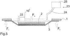
- Dispositif pour séparer un substrat de produit (4) d'un substrat porteur (2) relié au substrat de produit (4) par une couche de liaison (6), dans lequel le substrat de produit (4) est reçu sur un film flexible (3) qui présente une couche adhésive (3s) pour recevoir le substrat de produit (4) dans un tronçon de surface de contact (3k) du film (3), et dans lequel le film (3) est relié à un cadre de film (1) dans un tronçon de fixation (3b) du film (3) entourant le tronçon de surface de contact (3k), comprenant :- des décapants pour séparer le substrat de produit (4) du substrat porteur (2) par une force Fs agissant sur le substrat porteur (2), caractérisé en ce qu'au moins deux forces Ff1 et Ff2 pouvant être commandées de façon différente, réparties sur le pourtour, agissant sur le cadre de film (1) sur son pourtour, peuvent être appliquées en étant dirigées de façon opposée à la force Fs.
- Dispositif selon la revendication 1,
caractérisé en ce que
le film (3), en particulier par la force Fs et la force Ff, peut être tendu dans un tronçon de séparation (3a) situé entre le tronçon de surface de contact (3k) et le tronçon de fixation (3b). - Dispositif selon l'une des revendications précédentes, caractérisé en ce que
les décapants sont conçus pour agir de façon concentrique à partir du pourtour (4u) du substrat de produit (4) vers le centre (4z) du substrat de produit (4). - Procédé pour séparer un substrat de produit (4) d'un substrat porteur (2) relié au substrat de produit (4) par une couche de liaison (6), dans lequel le substrat de produit (4) est reçu sur un film flexible (3) qui présente une couche adhésive (3s) pour recevoir le substrat de produit (4) dans un tronçon de surface de contact (3k) du film (3), et dans lequel le film (3) est relié à un cadre de film (1) dans un tronçon de fixation (3b) du film (3) entourant le tronçon de surface de contact (3k), comprenant l'étape suivante :- séparation du substrat de produit (4) du substrat porteur (2) par une force Fs agissant sur le substrat porteur (2), caractérisé en ce qu'au moins deux forces Ff1 et Ff2 de la force Fs pouvant être commandées de façon différente, réparties sur le pourtour, agissant sur le cadre de film (1), agissent en étant dirigées de façon opposée à la force Fs.
- Procédé selon la revendication 4,
caractérisé en ce que
la séparation du substrat de produit (4) est effectuée de façon concentrique à partir du pourtour (4u) du substrat de produit (4) vers le centre (4z) du substrat de produit (4). - Procédé selon la revendication 4 ou 5,
caractérisé en ce que
le substrat de produit (4) est relié au substrat porteur (2) par une couche de liaison comprenant différentes colles.
Priority Applications (1)
| Application Number | Priority Date | Filing Date | Title |
|---|---|---|---|
| EP12179539.7A EP2523209B1 (fr) | 2010-04-23 | 2010-04-23 | Dispositif et procédé de séparation d'un substrat de produit et d'un substrat de support |
Applications Claiming Priority (2)
| Application Number | Priority Date | Filing Date | Title |
|---|---|---|---|
| EP10004313A EP2381464B1 (fr) | 2010-04-23 | 2010-04-23 | Dispositif et procédé de séparation d'un substrat de produit et d'un substrat de support |
| EP12179539.7A EP2523209B1 (fr) | 2010-04-23 | 2010-04-23 | Dispositif et procédé de séparation d'un substrat de produit et d'un substrat de support |
Related Parent Applications (2)
| Application Number | Title | Priority Date | Filing Date |
|---|---|---|---|
| EP10004313A Division EP2381464B1 (fr) | 2010-04-23 | 2010-04-23 | Dispositif et procédé de séparation d'un substrat de produit et d'un substrat de support |
| EP10004313.2 Division | 2010-04-23 |
Publications (2)
| Publication Number | Publication Date |
|---|---|
| EP2523209A1 EP2523209A1 (fr) | 2012-11-14 |
| EP2523209B1 true EP2523209B1 (fr) | 2017-03-08 |
Family
ID=42356878
Family Applications (3)
| Application Number | Title | Priority Date | Filing Date |
|---|---|---|---|
| EP10004313A Active EP2381464B1 (fr) | 2010-04-23 | 2010-04-23 | Dispositif et procédé de séparation d'un substrat de produit et d'un substrat de support |
| EP12179539.7A Active EP2523209B1 (fr) | 2010-04-23 | 2010-04-23 | Dispositif et procédé de séparation d'un substrat de produit et d'un substrat de support |
| EP12179537.1A Active EP2523208B1 (fr) | 2010-04-23 | 2010-04-23 | Dispositif et procédé de séparation d'un substrat de produit et d'un substrat de support |
Family Applications Before (1)
| Application Number | Title | Priority Date | Filing Date |
|---|---|---|---|
| EP10004313A Active EP2381464B1 (fr) | 2010-04-23 | 2010-04-23 | Dispositif et procédé de séparation d'un substrat de produit et d'un substrat de support |
Family Applications After (1)
| Application Number | Title | Priority Date | Filing Date |
|---|---|---|---|
| EP12179537.1A Active EP2523208B1 (fr) | 2010-04-23 | 2010-04-23 | Dispositif et procédé de séparation d'un substrat de produit et d'un substrat de support |
Country Status (8)
| Country | Link |
|---|---|
| US (3) | US9272501B2 (fr) |
| EP (3) | EP2381464B1 (fr) |
| JP (4) | JP5623623B2 (fr) |
| KR (3) | KR101476516B1 (fr) |
| CN (2) | CN103219265B (fr) |
| SG (1) | SG183305A1 (fr) |
| TW (3) | TWI520198B (fr) |
| WO (1) | WO2011131283A1 (fr) |
Families Citing this family (19)
| Publication number | Priority date | Publication date | Assignee | Title |
|---|---|---|---|---|
| EP2381464B1 (fr) * | 2010-04-23 | 2012-09-05 | EV Group GmbH | Dispositif et procédé de séparation d'un substrat de produit et d'un substrat de support |
| JP5558191B2 (ja) * | 2010-04-27 | 2014-07-23 | 東京応化工業株式会社 | 剥離装置及び剥離方法 |
| KR102064405B1 (ko) | 2014-02-04 | 2020-01-10 | 삼성디스플레이 주식회사 | 기판 박리 장치 및 그것을 이용한 기판 박리 방법 |
| KR102165162B1 (ko) | 2014-03-12 | 2020-10-14 | 삼성디스플레이 주식회사 | 기판 박리 장치 및 이를 이용한 소자 제조 방법 |
| JP6216727B2 (ja) * | 2014-05-08 | 2017-10-18 | 東京応化工業株式会社 | 支持体分離方法 |
| JP6268483B2 (ja) * | 2014-06-03 | 2018-01-31 | 旭硝子株式会社 | 積層体の剥離装置及び剥離方法並びに電子デバイスの製造方法 |
| SG11201603148VA (en) * | 2014-12-18 | 2016-07-28 | Ev Group E Thallner Gmbh | Method for bonding substrates |
| JP2016146429A (ja) * | 2015-02-09 | 2016-08-12 | トヨタ自動車株式会社 | 半導体装置の製造方法 |
| US10343417B2 (en) * | 2015-07-15 | 2019-07-09 | Hewlett-Packard Development Company, L.P. | Diagnostic plot for printing system |
| CN106053505A (zh) * | 2016-05-17 | 2016-10-26 | 深圳市宁深检验检测技术有限公司 | 一种表面覆膜金片金含量及金质量的快速测定方法 |
| JP7000129B2 (ja) * | 2017-11-15 | 2022-01-19 | 芝浦メカトロニクス株式会社 | 成膜装置 |
| JP6935306B2 (ja) * | 2017-11-16 | 2021-09-15 | 芝浦メカトロニクス株式会社 | 成膜装置 |
| HUE054704T2 (hu) * | 2018-12-06 | 2021-09-28 | Heraeus Deutschland Gmbh & Co Kg | Csomagolási egység szubsztrátok számára |
| JP7146354B2 (ja) | 2019-01-22 | 2022-10-04 | 株式会社ディスコ | キャリア板の除去方法 |
| KR102191204B1 (ko) * | 2019-07-31 | 2020-12-15 | 삼영공업 주식회사 | 접합판 분리 장치 및 접합판 분리 방법 |
| JP7262903B2 (ja) * | 2019-08-26 | 2023-04-24 | 株式会社ディスコ | キャリア板の除去方法 |
| JP7262904B2 (ja) * | 2019-08-26 | 2023-04-24 | 株式会社ディスコ | キャリア板の除去方法 |
| KR102298227B1 (ko) * | 2019-08-30 | 2021-09-06 | 주식회사 엘트린 | 디본딩 장치. |
| JP2022020952A (ja) * | 2020-07-21 | 2022-02-02 | 株式会社ディスコ | キャリア板の除去方法 |
Citations (1)
| Publication number | Priority date | Publication date | Assignee | Title |
|---|---|---|---|---|
| US20040166653A1 (en) * | 2002-12-16 | 2004-08-26 | Sebastien Kerdiles | Tools and methods for disuniting semiconductor wafers |
Family Cites Families (59)
| Publication number | Priority date | Publication date | Assignee | Title |
|---|---|---|---|---|
| US3988196A (en) | 1967-10-09 | 1976-10-26 | Western Electric Company, Inc. | Apparatus for transferring an oriented array of articles |
| US4826553A (en) * | 1987-06-18 | 1989-05-02 | The United States Of America As Represented By The Secretary Of The Air Force | Method for replicating an optical element |
| US5273615A (en) | 1992-04-06 | 1993-12-28 | Motorola, Inc. | Apparatus and method for handling fragile semiconductor wafers |
| JPH06275717A (ja) * | 1993-01-22 | 1994-09-30 | Mitsubishi Electric Corp | ウエハはがし方法 |
| JPH06268051A (ja) | 1993-03-10 | 1994-09-22 | Mitsubishi Electric Corp | ウエハ剥し装置 |
| JP4220580B2 (ja) | 1995-02-10 | 2009-02-04 | 三菱電機株式会社 | 半導体装置の製造装置 |
| JP3407835B2 (ja) | 1995-03-09 | 2003-05-19 | 東京応化工業株式会社 | 基板端縁部被膜の除去方法及び除去装置 |
| JP2004119975A (ja) | 1995-12-04 | 2004-04-15 | Renesas Technology Corp | Icカードの製造方法 |
| US6342434B1 (en) * | 1995-12-04 | 2002-01-29 | Hitachi, Ltd. | Methods of processing semiconductor wafer, and producing IC card, and carrier |
| DE19734635A1 (de) | 1997-08-11 | 1999-02-18 | Gen Semiconductor Ireland Macr | Verfahren und Vorrichtung zum Ablösen von Bauelementen von einer Folie |
| US6090687A (en) | 1998-07-29 | 2000-07-18 | Agilent Technolgies, Inc. | System and method for bonding and sealing microfabricated wafers to form a single structure having a vacuum chamber therein |
| JP2001196404A (ja) | 2000-01-11 | 2001-07-19 | Fujitsu Ltd | 半導体装置及びその製造方法 |
| JP3768069B2 (ja) | 2000-05-16 | 2006-04-19 | 信越半導体株式会社 | 半導体ウエーハの薄型化方法 |
| DE10048881A1 (de) | 2000-09-29 | 2002-03-07 | Infineon Technologies Ag | Vorrichtung und Verfahren zum planen Verbinden zweier Wafer für ein Dünnschleifen und ein Trennen eines Produkt-Wafers |
| JP2002237515A (ja) | 2001-02-07 | 2002-08-23 | Mitsubishi Gas Chem Co Inc | 薄葉化半導体基板の剥離装置および剥離法 |
| US6713880B2 (en) | 2001-02-07 | 2004-03-30 | Matsushita Electric Industrial Co., Ltd. | Semiconductor device and method for producing the same, and method for mounting semiconductor device |
| DE10108369A1 (de) | 2001-02-21 | 2002-08-29 | B L E Lab Equipment Gmbh | Verfahren und Vorrichtung zum Ablösen eines Halbleiterwafers von einem Träger |
| AT502233B1 (de) | 2001-06-07 | 2007-04-15 | Thallner Erich | Vorrichtung zum lösen eines trägers von einer halbleiterscheibe |
| DE60336050D1 (de) | 2002-03-27 | 2011-03-31 | Panasonic Corp | Herstellungsverfahren für ein mehrschichtiges optisches informationsaufzeichnungsmedium |
| JP4271409B2 (ja) * | 2002-05-22 | 2009-06-03 | リンテック株式会社 | 脆質材料の加工方法 |
| TWI258316B (en) | 2002-10-25 | 2006-07-11 | Ritdisplay Corp | FPD encapsulation apparatus and method for encapsulating ehereof |
| JP2004193237A (ja) | 2002-12-10 | 2004-07-08 | Disco Abrasive Syst Ltd | 粘着シートを具備するウェハー保持部材,及び粘着シートの剥離方法 |
| JP4364535B2 (ja) * | 2003-03-27 | 2009-11-18 | シャープ株式会社 | 半導体装置の製造方法 |
| JP4474854B2 (ja) * | 2003-07-02 | 2010-06-09 | Jsr株式会社 | 感放射線性接着剤組成物およびこれを用いたウェハーの加工方法 |
| DE10340409B4 (de) | 2003-09-02 | 2007-05-24 | Fraunhofer-Gesellschaft zur Förderung der angewandten Forschung e.V. | Trägerwafer und Verfahren zum Bearbeiten eines Halbleiterwafers unter Verwendung eines Trägerwafers |
| JP3912350B2 (ja) | 2003-09-22 | 2007-05-09 | 住友電気工業株式会社 | 半導体装置の製造方法 |
| JP4447280B2 (ja) | 2003-10-16 | 2010-04-07 | リンテック株式会社 | 表面保護用シートおよび半導体ウエハの研削方法 |
| JP2006135272A (ja) * | 2003-12-01 | 2006-05-25 | Tokyo Ohka Kogyo Co Ltd | 基板のサポートプレート及びサポートプレートの剥離方法 |
| JP2005191535A (ja) * | 2003-12-01 | 2005-07-14 | Tokyo Ohka Kogyo Co Ltd | 貼り付け装置および貼り付け方法 |
| DE102004018250A1 (de) | 2004-04-15 | 2005-11-03 | Infineon Technologies Ag | Wafer-Stabilisierungsvorrichtung und Verfahren zu dessen Herstellung |
| JP2005353859A (ja) | 2004-06-11 | 2005-12-22 | Taiyo Yuden Co Ltd | 半導体ウェハの剥離方法 |
| US7829152B2 (en) | 2006-10-05 | 2010-11-09 | Lam Research Corporation | Electroless plating method and apparatus |
| JP2006032506A (ja) | 2004-07-14 | 2006-02-02 | Taiyo Yuden Co Ltd | 半導体ウェハの剥離方法および剥離装置 |
| JP2006059861A (ja) * | 2004-08-17 | 2006-03-02 | Lintec Corp | 脆質部材の転着装置 |
| JP4679890B2 (ja) | 2004-11-29 | 2011-05-11 | 東京応化工業株式会社 | サポートプレートの貼り付け装置 |
| US9040420B2 (en) * | 2005-03-01 | 2015-05-26 | Semiconductor Energy Laboratory Co., Ltd. | Manufacturing method of semiconductor device including peeling layers from substrates by etching |
| JP4748518B2 (ja) * | 2005-07-20 | 2011-08-17 | 古河電気工業株式会社 | ダイシングダイボンドテープおよびダイシングテープ |
| JP4848153B2 (ja) | 2005-08-10 | 2011-12-28 | ルネサスエレクトロニクス株式会社 | 半導体装置の製造方法 |
| JP4721828B2 (ja) | 2005-08-31 | 2011-07-13 | 東京応化工業株式会社 | サポートプレートの剥離方法 |
| TW200730414A (en) * | 2005-11-18 | 2007-08-16 | Advanced Tech Materials | Material storage and dispensing containers and systems comprising same |
| JP4668052B2 (ja) | 2005-12-06 | 2011-04-13 | 東京応化工業株式会社 | 剥離装置 |
| DE102006000687B4 (de) | 2006-01-03 | 2010-09-09 | Thallner, Erich, Dipl.-Ing. | Kombination aus einem Träger und einem Wafer, Vorrichtung zum Trennen der Kombination und Verfahren zur Handhabung eines Trägers und eines Wafers |
| JP2008021929A (ja) * | 2006-07-14 | 2008-01-31 | Tokyo Ohka Kogyo Co Ltd | サポートプレート、搬送装置、剥離装置及び剥離方法 |
| JP5027460B2 (ja) * | 2006-07-28 | 2012-09-19 | 東京応化工業株式会社 | ウエハの接着方法、薄板化方法、及び剥離方法 |
| JP4847255B2 (ja) | 2006-08-30 | 2011-12-28 | 株式会社テオス | 半導体ウエーハの加工方法 |
| JP4402144B2 (ja) | 2006-09-29 | 2010-01-20 | 株式会社半導体エネルギー研究所 | 半導体装置の作製方法 |
| JP5238927B2 (ja) * | 2007-03-14 | 2013-07-17 | セミコンダクター・コンポーネンツ・インダストリーズ・リミテッド・ライアビリティ・カンパニー | 半導体装置の製造方法 |
| JP5090789B2 (ja) | 2007-05-30 | 2012-12-05 | 東京応化工業株式会社 | 貼り合わせ装置、接着剤の溶解を防ぐ方法、及び貼り合わせ方法 |
| JP4958287B2 (ja) | 2007-05-30 | 2012-06-20 | 東京応化工業株式会社 | 剥がし装置における剥離方法 |
| US20090017323A1 (en) * | 2007-07-13 | 2009-01-15 | 3M Innovative Properties Company | Layered body and method for manufacturing thin substrate using the layered body |
| JP5074940B2 (ja) | 2008-01-30 | 2012-11-14 | 東京応化工業株式会社 | 基板の処理方法 |
| JP2009182256A (ja) | 2008-01-31 | 2009-08-13 | Tokyo Ohka Kogyo Co Ltd | 基板の処理装置および基板の処理方法 |
| JP4965485B2 (ja) | 2008-02-29 | 2012-07-04 | 東京応化工業株式会社 | 処理液浸透ユニットおよび処理装置 |
| JP2010027720A (ja) | 2008-07-16 | 2010-02-04 | Shin Etsu Polymer Co Ltd | リングフレーム |
| WO2010023935A1 (fr) * | 2008-08-29 | 2010-03-04 | 株式会社ニコン | Dispositif et procédé d'alignement de substrats, et procédé de fabrication de semi-conducteur multicouche |
| TWM355799U (en) * | 2008-09-16 | 2009-05-01 | Ye Siang Entpr Co Ltd | Disassembling and assembling jig |
| EP2402981B1 (fr) | 2009-03-18 | 2013-07-10 | EV Group GmbH | Dispositif et procédé de séparation d'une tranche de silicium à partir d'un support |
| EP2381464B1 (fr) * | 2010-04-23 | 2012-09-05 | EV Group GmbH | Dispositif et procédé de séparation d'un substrat de produit et d'un substrat de support |
| SG11201405352PA (en) * | 2012-04-23 | 2014-09-26 | Univ Nanyang Tech | Apparatus and method for separating a stacked arrangement |
-
2010
- 2010-04-23 EP EP10004313A patent/EP2381464B1/fr active Active
- 2010-04-23 EP EP12179539.7A patent/EP2523209B1/fr active Active
- 2010-04-23 EP EP12179537.1A patent/EP2523208B1/fr active Active
-
2011
- 2011-03-29 CN CN201310126332.XA patent/CN103219265B/zh active Active
- 2011-03-29 WO PCT/EP2011/001556 patent/WO2011131283A1/fr active Application Filing
- 2011-03-29 KR KR1020127022017A patent/KR101476516B1/ko active IP Right Grant
- 2011-03-29 KR KR1020127032468A patent/KR101454985B1/ko active IP Right Grant
- 2011-03-29 CN CN201180011757.5A patent/CN103620732B/zh active Active
- 2011-03-29 JP JP2013504150A patent/JP5623623B2/ja active Active
- 2011-03-29 KR KR1020127032469A patent/KR101742347B1/ko active IP Right Grant
- 2011-03-29 SG SG2012060018A patent/SG183305A1/en unknown
- 2011-03-29 US US13/641,479 patent/US9272501B2/en active Active
- 2011-04-22 TW TW101145174A patent/TWI520198B/zh active
- 2011-04-22 TW TW100114153A patent/TWI421929B/zh active
- 2011-04-22 TW TW101145179A patent/TWI447793B/zh active
-
2013
- 2013-05-10 JP JP2013099954A patent/JP5714053B2/ja active Active
- 2013-06-18 US US13/920,458 patent/US9381729B2/en active Active
-
2014
- 2014-07-28 JP JP2014152881A patent/JP5997732B2/ja active Active
-
2015
- 2015-04-13 JP JP2015081502A patent/JP6099688B2/ja active Active
- 2015-05-19 US US14/715,691 patent/US9457552B2/en active Active
Patent Citations (1)
| Publication number | Priority date | Publication date | Assignee | Title |
|---|---|---|---|---|
| US20040166653A1 (en) * | 2002-12-16 | 2004-08-26 | Sebastien Kerdiles | Tools and methods for disuniting semiconductor wafers |
Also Published As
Similar Documents
| Publication | Publication Date | Title |
|---|---|---|
| EP2523209B1 (fr) | Dispositif et procédé de séparation d'un substrat de produit et d'un substrat de support | |
| EP2290679B1 (fr) | Dispositif et procédé de séparation d'un substrat de produit (par exemple, d'une tranche semi-conductrice) d'un substrat de support par déformation d'un film flexible monté sur un cadre | |
| EP2230683B1 (fr) | Dispositif et procédé de séparation d'une tranche de silicium à partir d'un support | |
| EP2382656B1 (fr) | Procédé de séparation pour système stratifié comprenant une tranche | |
| DE10260233B4 (de) | Verfahren zum Befestigen eines Werkstücks mit einem Feststoff an einem Werkstückträger und Werkstückträger | |
| DE112013000980B4 (de) | Verfahren zum temporären Verbinden eines Produktsubstrats mit einem Trägersubstrat sowie ein entsprechender Verbund | |
| DE112009000140T5 (de) | Verfahren zum reversiblen Anbringen eines Vorrichtungswafers an einem Trägersubstrat | |
| DE102010027703A1 (de) | Verfahren und Vorrichtung zum Entfernen eines reversibel angebrachten Vorrichtungswafers von einem Trägersubstrat | |
| WO2012097830A1 (fr) | Procédé servant à détacher un substrat produit d'un substrat support | |
| DE112016005452B4 (de) | Umgebungsschutzbarriere für einen Chip | |
| EP2553719B1 (fr) | Procédé de fabrication d'une tranche pourvue de puces à l'aide de deux tranches de support séparémment détachables avec des couches annulaires d'adhésion à différentes largeurs d'anneau | |
| DE10256247A1 (de) | Schichtverbund aus einer Trennschicht und einer Schutzschicht zum Schutze und zum Handling eines Wafers beim Dünnen, bei der Rückseitenbeschichtung und beim Vereinzeln | |
| WO2004032593A2 (fr) | Porte-substrat mince | |
| DE102004004476B3 (de) | Verfahren zum Aufbringen von Deckelstrukturen mittels eines biegsamen Trägers | |
| DE102019202564A1 (de) | Ablöseverfahren zum Ablösen eines Substrats von einer Trägerplatte | |
| DE4223215A1 (de) | Verfahren zur Bearbeitung von Siliziumwafern | |
| DE102006048800B4 (de) | Mehrlagenschichtsystem mit hartem Träger zum Trägern von dünnen Wafern bei der Halbleiterherstellung | |
| DE102006004834B4 (de) | Verfahren zum Behandeln von Wafern beim Abdünnen | |
| AT517638B1 (de) | Aufnahmeeinrichtung zur Handhabung strukturierter Substrate | |
| DE102020210751A1 (de) | Verfahren zum entfernen einer trägerplatte | |
| DE10262317B4 (de) | Verfahren zum Trennen eines Werkstücks von einem Werkstückträger |
Legal Events
| Date | Code | Title | Description |
|---|---|---|---|
| PUAI | Public reference made under article 153(3) epc to a published international application that has entered the european phase |
Free format text: ORIGINAL CODE: 0009012 |
|
| AC | Divisional application: reference to earlier application |
Ref document number: 2381464 Country of ref document: EP Kind code of ref document: P |
|
| AK | Designated contracting states |
Kind code of ref document: A1 Designated state(s): AT BE BG CH CY CZ DE DK EE ES FI FR GB GR HR HU IE IS IT LI LT LU LV MC MK MT NL NO PL PT RO SE SI SK SM TR |
|
| 17P | Request for examination filed |
Effective date: 20130307 |
|
| 17Q | First examination report despatched |
Effective date: 20141212 |
|
| REG | Reference to a national code |
Ref country code: DE Ref legal event code: R079 Ref document number: 502010013291 Country of ref document: DE Free format text: PREVIOUS MAIN CLASS: H01L0021000000 Ipc: H01L0021670000 |
|
| GRAP | Despatch of communication of intention to grant a patent |
Free format text: ORIGINAL CODE: EPIDOSNIGR1 |
|
| RIC1 | Information provided on ipc code assigned before grant |
Ipc: B32B 43/00 20060101ALN20160912BHEP Ipc: H01L 21/673 20060101ALI20160912BHEP Ipc: H01L 21/00 20060101ALI20160912BHEP Ipc: B32B 37/00 20060101ALI20160912BHEP Ipc: H01L 21/67 20060101AFI20160912BHEP Ipc: B32B 38/00 20060101ALN20160912BHEP Ipc: H01L 21/687 20060101ALI20160912BHEP Ipc: B32B 38/10 20060101ALI20160912BHEP |
|
| RIC1 | Information provided on ipc code assigned before grant |
Ipc: B32B 43/00 20060101ALN20160923BHEP Ipc: H01L 21/687 20060101ALI20160923BHEP Ipc: H01L 21/00 20060101ALI20160923BHEP Ipc: B32B 38/10 20060101ALI20160923BHEP Ipc: H01L 21/67 20060101AFI20160923BHEP Ipc: B32B 37/00 20060101ALI20160923BHEP Ipc: H01L 21/673 20060101ALI20160923BHEP Ipc: B32B 38/00 20060101ALN20160923BHEP |
|
| INTG | Intention to grant announced |
Effective date: 20161011 |
|
| STAA | Information on the status of an ep patent application or granted ep patent |
Free format text: STATUS: GRANT OF PATENT IS INTENDED |
|
| GRAS | Grant fee paid |
Free format text: ORIGINAL CODE: EPIDOSNIGR3 |
|
| GRAA | (expected) grant |
Free format text: ORIGINAL CODE: 0009210 |
|
| STAA | Information on the status of an ep patent application or granted ep patent |
Free format text: STATUS: THE PATENT HAS BEEN GRANTED |
|
| AC | Divisional application: reference to earlier application |
Ref document number: 2381464 Country of ref document: EP Kind code of ref document: P |
|
| AK | Designated contracting states |
Kind code of ref document: B1 Designated state(s): AT BE BG CH CY CZ DE DK EE ES FI FR GB GR HR HU IE IS IT LI LT LU LV MC MK MT NL NO PL PT RO SE SI SK SM TR |
|
| REG | Reference to a national code |
Ref country code: GB Ref legal event code: FG4D Free format text: NOT ENGLISH |
|
| REG | Reference to a national code |
Ref country code: CH Ref legal event code: EP Ref country code: AT Ref legal event code: REF Ref document number: 874228 Country of ref document: AT Kind code of ref document: T Effective date: 20170315 |
|
| REG | Reference to a national code |
Ref country code: IE Ref legal event code: FG4D Free format text: LANGUAGE OF EP DOCUMENT: GERMAN |
|
| REG | Reference to a national code |
Ref country code: DE Ref legal event code: R096 Ref document number: 502010013291 Country of ref document: DE |
|
| REG | Reference to a national code |
Ref country code: FR Ref legal event code: PLFP Year of fee payment: 8 |
|
| REG | Reference to a national code |
Ref country code: LT Ref legal event code: MG4D |
|
| REG | Reference to a national code |
Ref country code: NL Ref legal event code: MP Effective date: 20170308 |
|
| PG25 | Lapsed in a contracting state [announced via postgrant information from national office to epo] |
Ref country code: NO Free format text: LAPSE BECAUSE OF FAILURE TO SUBMIT A TRANSLATION OF THE DESCRIPTION OR TO PAY THE FEE WITHIN THE PRESCRIBED TIME-LIMIT Effective date: 20170608 Ref country code: GR Free format text: LAPSE BECAUSE OF FAILURE TO SUBMIT A TRANSLATION OF THE DESCRIPTION OR TO PAY THE FEE WITHIN THE PRESCRIBED TIME-LIMIT Effective date: 20170609 Ref country code: LT Free format text: LAPSE BECAUSE OF FAILURE TO SUBMIT A TRANSLATION OF THE DESCRIPTION OR TO PAY THE FEE WITHIN THE PRESCRIBED TIME-LIMIT Effective date: 20170308 Ref country code: HR Free format text: LAPSE BECAUSE OF FAILURE TO SUBMIT A TRANSLATION OF THE DESCRIPTION OR TO PAY THE FEE WITHIN THE PRESCRIBED TIME-LIMIT Effective date: 20170308 Ref country code: FI Free format text: LAPSE BECAUSE OF FAILURE TO SUBMIT A TRANSLATION OF THE DESCRIPTION OR TO PAY THE FEE WITHIN THE PRESCRIBED TIME-LIMIT Effective date: 20170308 |
|
| PG25 | Lapsed in a contracting state [announced via postgrant information from national office to epo] |
Ref country code: SE Free format text: LAPSE BECAUSE OF FAILURE TO SUBMIT A TRANSLATION OF THE DESCRIPTION OR TO PAY THE FEE WITHIN THE PRESCRIBED TIME-LIMIT Effective date: 20170308 Ref country code: LV Free format text: LAPSE BECAUSE OF FAILURE TO SUBMIT A TRANSLATION OF THE DESCRIPTION OR TO PAY THE FEE WITHIN THE PRESCRIBED TIME-LIMIT Effective date: 20170308 Ref country code: BG Free format text: LAPSE BECAUSE OF FAILURE TO SUBMIT A TRANSLATION OF THE DESCRIPTION OR TO PAY THE FEE WITHIN THE PRESCRIBED TIME-LIMIT Effective date: 20170608 Ref country code: ES Free format text: LAPSE BECAUSE OF FAILURE TO SUBMIT A TRANSLATION OF THE DESCRIPTION OR TO PAY THE FEE WITHIN THE PRESCRIBED TIME-LIMIT Effective date: 20170308 |
|
| PG25 | Lapsed in a contracting state [announced via postgrant information from national office to epo] |
Ref country code: NL Free format text: LAPSE BECAUSE OF FAILURE TO SUBMIT A TRANSLATION OF THE DESCRIPTION OR TO PAY THE FEE WITHIN THE PRESCRIBED TIME-LIMIT Effective date: 20170308 |
|
| PG25 | Lapsed in a contracting state [announced via postgrant information from national office to epo] |
Ref country code: CZ Free format text: LAPSE BECAUSE OF FAILURE TO SUBMIT A TRANSLATION OF THE DESCRIPTION OR TO PAY THE FEE WITHIN THE PRESCRIBED TIME-LIMIT Effective date: 20170308 Ref country code: RO Free format text: LAPSE BECAUSE OF FAILURE TO SUBMIT A TRANSLATION OF THE DESCRIPTION OR TO PAY THE FEE WITHIN THE PRESCRIBED TIME-LIMIT Effective date: 20170308 Ref country code: SK Free format text: LAPSE BECAUSE OF FAILURE TO SUBMIT A TRANSLATION OF THE DESCRIPTION OR TO PAY THE FEE WITHIN THE PRESCRIBED TIME-LIMIT Effective date: 20170308 Ref country code: EE Free format text: LAPSE BECAUSE OF FAILURE TO SUBMIT A TRANSLATION OF THE DESCRIPTION OR TO PAY THE FEE WITHIN THE PRESCRIBED TIME-LIMIT Effective date: 20170308 Ref country code: IT Free format text: LAPSE BECAUSE OF FAILURE TO SUBMIT A TRANSLATION OF THE DESCRIPTION OR TO PAY THE FEE WITHIN THE PRESCRIBED TIME-LIMIT Effective date: 20170308 |
|
| PG25 | Lapsed in a contracting state [announced via postgrant information from national office to epo] |
Ref country code: PL Free format text: LAPSE BECAUSE OF FAILURE TO SUBMIT A TRANSLATION OF THE DESCRIPTION OR TO PAY THE FEE WITHIN THE PRESCRIBED TIME-LIMIT Effective date: 20170308 Ref country code: IS Free format text: LAPSE BECAUSE OF FAILURE TO SUBMIT A TRANSLATION OF THE DESCRIPTION OR TO PAY THE FEE WITHIN THE PRESCRIBED TIME-LIMIT Effective date: 20170708 Ref country code: SM Free format text: LAPSE BECAUSE OF FAILURE TO SUBMIT A TRANSLATION OF THE DESCRIPTION OR TO PAY THE FEE WITHIN THE PRESCRIBED TIME-LIMIT Effective date: 20170308 Ref country code: PT Free format text: LAPSE BECAUSE OF FAILURE TO SUBMIT A TRANSLATION OF THE DESCRIPTION OR TO PAY THE FEE WITHIN THE PRESCRIBED TIME-LIMIT Effective date: 20170710 |
|
| REG | Reference to a national code |
Ref country code: CH Ref legal event code: PL |
|
| REG | Reference to a national code |
Ref country code: DE Ref legal event code: R097 Ref document number: 502010013291 Country of ref document: DE |
|
| PLBE | No opposition filed within time limit |
Free format text: ORIGINAL CODE: 0009261 |
|
| STAA | Information on the status of an ep patent application or granted ep patent |
Free format text: STATUS: NO OPPOSITION FILED WITHIN TIME LIMIT |
|
| REG | Reference to a national code |
Ref country code: IE Ref legal event code: MM4A |
|
| PG25 | Lapsed in a contracting state [announced via postgrant information from national office to epo] |
Ref country code: MC Free format text: LAPSE BECAUSE OF FAILURE TO SUBMIT A TRANSLATION OF THE DESCRIPTION OR TO PAY THE FEE WITHIN THE PRESCRIBED TIME-LIMIT Effective date: 20170308 Ref country code: DK Free format text: LAPSE BECAUSE OF FAILURE TO SUBMIT A TRANSLATION OF THE DESCRIPTION OR TO PAY THE FEE WITHIN THE PRESCRIBED TIME-LIMIT Effective date: 20170308 |
|
| 26N | No opposition filed |
Effective date: 20171211 |
|
| PG25 | Lapsed in a contracting state [announced via postgrant information from national office to epo] |
Ref country code: SI Free format text: LAPSE BECAUSE OF FAILURE TO SUBMIT A TRANSLATION OF THE DESCRIPTION OR TO PAY THE FEE WITHIN THE PRESCRIBED TIME-LIMIT Effective date: 20170308 Ref country code: CH Free format text: LAPSE BECAUSE OF NON-PAYMENT OF DUE FEES Effective date: 20170430 Ref country code: LU Free format text: LAPSE BECAUSE OF NON-PAYMENT OF DUE FEES Effective date: 20170423 Ref country code: LI Free format text: LAPSE BECAUSE OF NON-PAYMENT OF DUE FEES Effective date: 20170430 |
|
| REG | Reference to a national code |
Ref country code: BE Ref legal event code: MM Effective date: 20170430 |
|
| REG | Reference to a national code |
Ref country code: FR Ref legal event code: PLFP Year of fee payment: 9 |
|
| PG25 | Lapsed in a contracting state [announced via postgrant information from national office to epo] |
Ref country code: IE Free format text: LAPSE BECAUSE OF NON-PAYMENT OF DUE FEES Effective date: 20170423 |
|
| PG25 | Lapsed in a contracting state [announced via postgrant information from national office to epo] |
Ref country code: BE Free format text: LAPSE BECAUSE OF NON-PAYMENT OF DUE FEES Effective date: 20170430 |
|
| PG25 | Lapsed in a contracting state [announced via postgrant information from national office to epo] |
Ref country code: MT Free format text: LAPSE BECAUSE OF FAILURE TO SUBMIT A TRANSLATION OF THE DESCRIPTION OR TO PAY THE FEE WITHIN THE PRESCRIBED TIME-LIMIT Effective date: 20170308 |
|
| PG25 | Lapsed in a contracting state [announced via postgrant information from national office to epo] |
Ref country code: HU Free format text: LAPSE BECAUSE OF FAILURE TO SUBMIT A TRANSLATION OF THE DESCRIPTION OR TO PAY THE FEE WITHIN THE PRESCRIBED TIME-LIMIT; INVALID AB INITIO Effective date: 20100423 |
|
| PG25 | Lapsed in a contracting state [announced via postgrant information from national office to epo] |
Ref country code: CY Free format text: LAPSE BECAUSE OF NON-PAYMENT OF DUE FEES Effective date: 20170308 |
|
| PG25 | Lapsed in a contracting state [announced via postgrant information from national office to epo] |
Ref country code: MK Free format text: LAPSE BECAUSE OF FAILURE TO SUBMIT A TRANSLATION OF THE DESCRIPTION OR TO PAY THE FEE WITHIN THE PRESCRIBED TIME-LIMIT Effective date: 20170308 |
|
| PG25 | Lapsed in a contracting state [announced via postgrant information from national office to epo] |
Ref country code: TR Free format text: LAPSE BECAUSE OF FAILURE TO SUBMIT A TRANSLATION OF THE DESCRIPTION OR TO PAY THE FEE WITHIN THE PRESCRIBED TIME-LIMIT Effective date: 20170308 |
|
| PGFP | Annual fee paid to national office [announced via postgrant information from national office to epo] |
Ref country code: FR Payment date: 20230417 Year of fee payment: 14 Ref country code: DE Payment date: 20230427 Year of fee payment: 14 |
|
| PGFP | Annual fee paid to national office [announced via postgrant information from national office to epo] |
Ref country code: AT Payment date: 20230414 Year of fee payment: 14 |
|
| PGFP | Annual fee paid to national office [announced via postgrant information from national office to epo] |
Ref country code: GB Payment date: 20230404 Year of fee payment: 14 |