EP2523208B1 - Dispositif et procédé de séparation d'un substrat de produit et d'un substrat de support - Google Patents
Dispositif et procédé de séparation d'un substrat de produit et d'un substrat de support Download PDFInfo
- Publication number
- EP2523208B1 EP2523208B1 EP12179537.1A EP12179537A EP2523208B1 EP 2523208 B1 EP2523208 B1 EP 2523208B1 EP 12179537 A EP12179537 A EP 12179537A EP 2523208 B1 EP2523208 B1 EP 2523208B1
- Authority
- EP
- European Patent Office
- Prior art keywords
- solvent
- product substrate
- bonding layer
- film
- substrate
- Prior art date
- Legal status (The legal status is an assumption and is not a legal conclusion. Google has not performed a legal analysis and makes no representation as to the accuracy of the status listed.)
- Active
Links
- 239000000758 substrate Substances 0.000 title claims description 94
- 238000000034 method Methods 0.000 title claims description 27
- 239000002904 solvent Substances 0.000 claims description 61
- 239000010410 layer Substances 0.000 claims description 34
- 239000000853 adhesive Substances 0.000 claims description 7
- 230000001070 adhesive effect Effects 0.000 claims description 7
- 239000012790 adhesive layer Substances 0.000 claims description 5
- 239000012530 fluid Substances 0.000 claims description 3
- 239000000047 product Substances 0.000 description 43
- 238000004090 dissolution Methods 0.000 description 7
- 239000002131 composite material Substances 0.000 description 5
- 235000012431 wafers Nutrition 0.000 description 5
- 239000012876 carrier material Substances 0.000 description 2
- 238000010438 heat treatment Methods 0.000 description 2
- 239000000463 material Substances 0.000 description 2
- 239000004065 semiconductor Substances 0.000 description 2
- 239000000126 substance Substances 0.000 description 2
- XUIMIQQOPSSXEZ-UHFFFAOYSA-N Silicon Chemical compound [Si] XUIMIQQOPSSXEZ-UHFFFAOYSA-N 0.000 description 1
- 239000004809 Teflon Substances 0.000 description 1
- 229920006362 Teflon® Polymers 0.000 description 1
- 239000006227 byproduct Substances 0.000 description 1
- 238000011161 development Methods 0.000 description 1
- 230000018109 developmental process Effects 0.000 description 1
- 230000000694 effects Effects 0.000 description 1
- 229920002313 fluoropolymer Polymers 0.000 description 1
- 239000004811 fluoropolymer Substances 0.000 description 1
- 239000011521 glass Substances 0.000 description 1
- 238000007654 immersion Methods 0.000 description 1
- 238000003780 insertion Methods 0.000 description 1
- 230000037431 insertion Effects 0.000 description 1
- 238000000926 separation method Methods 0.000 description 1
- 229910052710 silicon Inorganic materials 0.000 description 1
- 239000010703 silicon Substances 0.000 description 1
- 229920001169 thermoplastic Polymers 0.000 description 1
- 239000004416 thermosoftening plastic Substances 0.000 description 1
Images
Classifications
-
- H—ELECTRICITY
- H01—ELECTRIC ELEMENTS
- H01L—SEMICONDUCTOR DEVICES NOT COVERED BY CLASS H10
- H01L21/00—Processes or apparatus adapted for the manufacture or treatment of semiconductor or solid state devices or of parts thereof
- H01L21/67—Apparatus specially adapted for handling semiconductor or electric solid state devices during manufacture or treatment thereof; Apparatus specially adapted for handling wafers during manufacture or treatment of semiconductor or electric solid state devices or components ; Apparatus not specifically provided for elsewhere
- H01L21/67005—Apparatus not specifically provided for elsewhere
- H01L21/67011—Apparatus for manufacture or treatment
- H01L21/67092—Apparatus for mechanical treatment
-
- B—PERFORMING OPERATIONS; TRANSPORTING
- B32—LAYERED PRODUCTS
- B32B—LAYERED PRODUCTS, i.e. PRODUCTS BUILT-UP OF STRATA OF FLAT OR NON-FLAT, e.g. CELLULAR OR HONEYCOMB, FORM
- B32B38/00—Ancillary operations in connection with laminating processes
- B32B38/10—Removing layers, or parts of layers, mechanically or chemically
-
- H—ELECTRICITY
- H01—ELECTRIC ELEMENTS
- H01L—SEMICONDUCTOR DEVICES NOT COVERED BY CLASS H10
- H01L21/00—Processes or apparatus adapted for the manufacture or treatment of semiconductor or solid state devices or of parts thereof
- H01L21/02—Manufacture or treatment of semiconductor devices or of parts thereof
-
- B—PERFORMING OPERATIONS; TRANSPORTING
- B32—LAYERED PRODUCTS
- B32B—LAYERED PRODUCTS, i.e. PRODUCTS BUILT-UP OF STRATA OF FLAT OR NON-FLAT, e.g. CELLULAR OR HONEYCOMB, FORM
- B32B37/00—Methods or apparatus for laminating, e.g. by curing or by ultrasonic bonding
- B32B37/02—Methods or apparatus for laminating, e.g. by curing or by ultrasonic bonding characterised by a sequence of laminating steps, e.g. by adding new layers at consecutive laminating stations
- B32B37/025—Transfer laminating
-
- H—ELECTRICITY
- H01—ELECTRIC ELEMENTS
- H01L—SEMICONDUCTOR DEVICES NOT COVERED BY CLASS H10
- H01L21/00—Processes or apparatus adapted for the manufacture or treatment of semiconductor or solid state devices or of parts thereof
- H01L21/67—Apparatus specially adapted for handling semiconductor or electric solid state devices during manufacture or treatment thereof; Apparatus specially adapted for handling wafers during manufacture or treatment of semiconductor or electric solid state devices or components ; Apparatus not specifically provided for elsewhere
- H01L21/67005—Apparatus not specifically provided for elsewhere
- H01L21/67011—Apparatus for manufacture or treatment
- H01L21/67132—Apparatus for placing on an insulating substrate, e.g. tape
-
- H—ELECTRICITY
- H01—ELECTRIC ELEMENTS
- H01L—SEMICONDUCTOR DEVICES NOT COVERED BY CLASS H10
- H01L21/00—Processes or apparatus adapted for the manufacture or treatment of semiconductor or solid state devices or of parts thereof
- H01L21/67—Apparatus specially adapted for handling semiconductor or electric solid state devices during manufacture or treatment thereof; Apparatus specially adapted for handling wafers during manufacture or treatment of semiconductor or electric solid state devices or components ; Apparatus not specifically provided for elsewhere
- H01L21/67005—Apparatus not specifically provided for elsewhere
- H01L21/67011—Apparatus for manufacture or treatment
- H01L21/6715—Apparatus for applying a liquid, a resin, an ink or the like
-
- H—ELECTRICITY
- H01—ELECTRIC ELEMENTS
- H01L—SEMICONDUCTOR DEVICES NOT COVERED BY CLASS H10
- H01L21/00—Processes or apparatus adapted for the manufacture or treatment of semiconductor or solid state devices or of parts thereof
- H01L21/67—Apparatus specially adapted for handling semiconductor or electric solid state devices during manufacture or treatment thereof; Apparatus specially adapted for handling wafers during manufacture or treatment of semiconductor or electric solid state devices or components ; Apparatus not specifically provided for elsewhere
- H01L21/677—Apparatus specially adapted for handling semiconductor or electric solid state devices during manufacture or treatment thereof; Apparatus specially adapted for handling wafers during manufacture or treatment of semiconductor or electric solid state devices or components ; Apparatus not specifically provided for elsewhere for conveying, e.g. between different workstations
-
- B—PERFORMING OPERATIONS; TRANSPORTING
- B32—LAYERED PRODUCTS
- B32B—LAYERED PRODUCTS, i.e. PRODUCTS BUILT-UP OF STRATA OF FLAT OR NON-FLAT, e.g. CELLULAR OR HONEYCOMB, FORM
- B32B38/00—Ancillary operations in connection with laminating processes
- B32B2038/0052—Other operations not otherwise provided for
-
- B—PERFORMING OPERATIONS; TRANSPORTING
- B32—LAYERED PRODUCTS
- B32B—LAYERED PRODUCTS, i.e. PRODUCTS BUILT-UP OF STRATA OF FLAT OR NON-FLAT, e.g. CELLULAR OR HONEYCOMB, FORM
- B32B2307/00—Properties of the layers or laminate
- B32B2307/50—Properties of the layers or laminate having particular mechanical properties
- B32B2307/546—Flexural strength; Flexion stiffness
-
- B—PERFORMING OPERATIONS; TRANSPORTING
- B32—LAYERED PRODUCTS
- B32B—LAYERED PRODUCTS, i.e. PRODUCTS BUILT-UP OF STRATA OF FLAT OR NON-FLAT, e.g. CELLULAR OR HONEYCOMB, FORM
- B32B2310/00—Treatment by energy or chemical effects
- B32B2310/04—Treatment by energy or chemical effects using liquids, gas or steam
- B32B2310/0409—Treatment by energy or chemical effects using liquids, gas or steam using liquids
- B32B2310/0418—Treatment by energy or chemical effects using liquids, gas or steam using liquids other than water
-
- B—PERFORMING OPERATIONS; TRANSPORTING
- B32—LAYERED PRODUCTS
- B32B—LAYERED PRODUCTS, i.e. PRODUCTS BUILT-UP OF STRATA OF FLAT OR NON-FLAT, e.g. CELLULAR OR HONEYCOMB, FORM
- B32B43/00—Operations specially adapted for layered products and not otherwise provided for, e.g. repairing; Apparatus therefor
- B32B43/006—Delaminating
-
- H—ELECTRICITY
- H01—ELECTRIC ELEMENTS
- H01L—SEMICONDUCTOR DEVICES NOT COVERED BY CLASS H10
- H01L21/00—Processes or apparatus adapted for the manufacture or treatment of semiconductor or solid state devices or of parts thereof
- H01L21/67—Apparatus specially adapted for handling semiconductor or electric solid state devices during manufacture or treatment thereof; Apparatus specially adapted for handling wafers during manufacture or treatment of semiconductor or electric solid state devices or components ; Apparatus not specifically provided for elsewhere
- H01L21/673—Apparatus specially adapted for handling semiconductor or electric solid state devices during manufacture or treatment thereof; Apparatus specially adapted for handling wafers during manufacture or treatment of semiconductor or electric solid state devices or components ; Apparatus not specifically provided for elsewhere using specially adapted carriers or holders; Fixing the workpieces on such carriers or holders
- H01L21/67346—Apparatus specially adapted for handling semiconductor or electric solid state devices during manufacture or treatment thereof; Apparatus specially adapted for handling wafers during manufacture or treatment of semiconductor or electric solid state devices or components ; Apparatus not specifically provided for elsewhere using specially adapted carriers or holders; Fixing the workpieces on such carriers or holders characterized by being specially adapted for supporting a single substrate or by comprising a stack of such individual supports
-
- H—ELECTRICITY
- H01—ELECTRIC ELEMENTS
- H01L—SEMICONDUCTOR DEVICES NOT COVERED BY CLASS H10
- H01L21/00—Processes or apparatus adapted for the manufacture or treatment of semiconductor or solid state devices or of parts thereof
- H01L21/67—Apparatus specially adapted for handling semiconductor or electric solid state devices during manufacture or treatment thereof; Apparatus specially adapted for handling wafers during manufacture or treatment of semiconductor or electric solid state devices or components ; Apparatus not specifically provided for elsewhere
- H01L21/683—Apparatus specially adapted for handling semiconductor or electric solid state devices during manufacture or treatment thereof; Apparatus specially adapted for handling wafers during manufacture or treatment of semiconductor or electric solid state devices or components ; Apparatus not specifically provided for elsewhere for supporting or gripping
- H01L21/687—Apparatus specially adapted for handling semiconductor or electric solid state devices during manufacture or treatment thereof; Apparatus specially adapted for handling wafers during manufacture or treatment of semiconductor or electric solid state devices or components ; Apparatus not specifically provided for elsewhere for supporting or gripping using mechanical means, e.g. chucks, clamps or pinches
- H01L21/68714—Apparatus specially adapted for handling semiconductor or electric solid state devices during manufacture or treatment thereof; Apparatus specially adapted for handling wafers during manufacture or treatment of semiconductor or electric solid state devices or components ; Apparatus not specifically provided for elsewhere for supporting or gripping using mechanical means, e.g. chucks, clamps or pinches the wafers being placed on a susceptor, stage or support
- H01L21/68721—Apparatus specially adapted for handling semiconductor or electric solid state devices during manufacture or treatment thereof; Apparatus specially adapted for handling wafers during manufacture or treatment of semiconductor or electric solid state devices or components ; Apparatus not specifically provided for elsewhere for supporting or gripping using mechanical means, e.g. chucks, clamps or pinches the wafers being placed on a susceptor, stage or support characterised by edge clamping, e.g. clamping ring
-
- H—ELECTRICITY
- H01—ELECTRIC ELEMENTS
- H01L—SEMICONDUCTOR DEVICES NOT COVERED BY CLASS H10
- H01L21/00—Processes or apparatus adapted for the manufacture or treatment of semiconductor or solid state devices or of parts thereof
- H01L21/67—Apparatus specially adapted for handling semiconductor or electric solid state devices during manufacture or treatment thereof; Apparatus specially adapted for handling wafers during manufacture or treatment of semiconductor or electric solid state devices or components ; Apparatus not specifically provided for elsewhere
- H01L21/683—Apparatus specially adapted for handling semiconductor or electric solid state devices during manufacture or treatment thereof; Apparatus specially adapted for handling wafers during manufacture or treatment of semiconductor or electric solid state devices or components ; Apparatus not specifically provided for elsewhere for supporting or gripping
- H01L21/687—Apparatus specially adapted for handling semiconductor or electric solid state devices during manufacture or treatment thereof; Apparatus specially adapted for handling wafers during manufacture or treatment of semiconductor or electric solid state devices or components ; Apparatus not specifically provided for elsewhere for supporting or gripping using mechanical means, e.g. chucks, clamps or pinches
- H01L21/68714—Apparatus specially adapted for handling semiconductor or electric solid state devices during manufacture or treatment thereof; Apparatus specially adapted for handling wafers during manufacture or treatment of semiconductor or electric solid state devices or components ; Apparatus not specifically provided for elsewhere for supporting or gripping using mechanical means, e.g. chucks, clamps or pinches the wafers being placed on a susceptor, stage or support
- H01L21/68771—Apparatus specially adapted for handling semiconductor or electric solid state devices during manufacture or treatment thereof; Apparatus specially adapted for handling wafers during manufacture or treatment of semiconductor or electric solid state devices or components ; Apparatus not specifically provided for elsewhere for supporting or gripping using mechanical means, e.g. chucks, clamps or pinches the wafers being placed on a susceptor, stage or support characterised by supporting more than one semiconductor substrate
-
- H—ELECTRICITY
- H01—ELECTRIC ELEMENTS
- H01L—SEMICONDUCTOR DEVICES NOT COVERED BY CLASS H10
- H01L2221/00—Processes or apparatus adapted for the manufacture or treatment of semiconductor or solid state devices or of parts thereof covered by H01L21/00
- H01L2221/67—Apparatus for handling semiconductor or electric solid state devices during manufacture or treatment thereof; Apparatus for handling wafers during manufacture or treatment of semiconductor or electric solid state devices or components; Apparatus not specifically provided for elsewhere
- H01L2221/683—Apparatus for handling semiconductor or electric solid state devices during manufacture or treatment thereof; Apparatus for handling wafers during manufacture or treatment of semiconductor or electric solid state devices or components; Apparatus not specifically provided for elsewhere for supporting or gripping
- H01L2221/68304—Apparatus for handling semiconductor or electric solid state devices during manufacture or treatment thereof; Apparatus for handling wafers during manufacture or treatment of semiconductor or electric solid state devices or components; Apparatus not specifically provided for elsewhere for supporting or gripping using temporarily an auxiliary support
- H01L2221/68381—Details of chemical or physical process used for separating the auxiliary support from a device or wafer
- H01L2221/68386—Separation by peeling
-
- Y—GENERAL TAGGING OF NEW TECHNOLOGICAL DEVELOPMENTS; GENERAL TAGGING OF CROSS-SECTIONAL TECHNOLOGIES SPANNING OVER SEVERAL SECTIONS OF THE IPC; TECHNICAL SUBJECTS COVERED BY FORMER USPC CROSS-REFERENCE ART COLLECTIONS [XRACs] AND DIGESTS
- Y10—TECHNICAL SUBJECTS COVERED BY FORMER USPC
- Y10T—TECHNICAL SUBJECTS COVERED BY FORMER US CLASSIFICATION
- Y10T156/00—Adhesive bonding and miscellaneous chemical manufacture
- Y10T156/11—Methods of delaminating, per se; i.e., separating at bonding face
- Y10T156/1111—Using solvent during delaminating [e.g., water dissolving adhesive at bonding face during delamination, etc.]
-
- Y—GENERAL TAGGING OF NEW TECHNOLOGICAL DEVELOPMENTS; GENERAL TAGGING OF CROSS-SECTIONAL TECHNOLOGIES SPANNING OVER SEVERAL SECTIONS OF THE IPC; TECHNICAL SUBJECTS COVERED BY FORMER USPC CROSS-REFERENCE ART COLLECTIONS [XRACs] AND DIGESTS
- Y10—TECHNICAL SUBJECTS COVERED BY FORMER USPC
- Y10T—TECHNICAL SUBJECTS COVERED BY FORMER US CLASSIFICATION
- Y10T156/00—Adhesive bonding and miscellaneous chemical manufacture
- Y10T156/11—Methods of delaminating, per se; i.e., separating at bonding face
- Y10T156/1168—Gripping and pulling work apart during delaminating
- Y10T156/1179—Gripping and pulling work apart during delaminating with poking during delaminating [e.g., jabbing, etc.]
-
- Y—GENERAL TAGGING OF NEW TECHNOLOGICAL DEVELOPMENTS; GENERAL TAGGING OF CROSS-SECTIONAL TECHNOLOGIES SPANNING OVER SEVERAL SECTIONS OF THE IPC; TECHNICAL SUBJECTS COVERED BY FORMER USPC CROSS-REFERENCE ART COLLECTIONS [XRACs] AND DIGESTS
- Y10—TECHNICAL SUBJECTS COVERED BY FORMER USPC
- Y10T—TECHNICAL SUBJECTS COVERED BY FORMER US CLASSIFICATION
- Y10T156/00—Adhesive bonding and miscellaneous chemical manufacture
- Y10T156/19—Delaminating means
- Y10T156/1922—Vibrating delaminating means
-
- Y—GENERAL TAGGING OF NEW TECHNOLOGICAL DEVELOPMENTS; GENERAL TAGGING OF CROSS-SECTIONAL TECHNOLOGIES SPANNING OVER SEVERAL SECTIONS OF THE IPC; TECHNICAL SUBJECTS COVERED BY FORMER USPC CROSS-REFERENCE ART COLLECTIONS [XRACs] AND DIGESTS
- Y10—TECHNICAL SUBJECTS COVERED BY FORMER USPC
- Y10T—TECHNICAL SUBJECTS COVERED BY FORMER US CLASSIFICATION
- Y10T156/00—Adhesive bonding and miscellaneous chemical manufacture
- Y10T156/19—Delaminating means
- Y10T156/1928—Differential fluid pressure delaminating means
-
- Y—GENERAL TAGGING OF NEW TECHNOLOGICAL DEVELOPMENTS; GENERAL TAGGING OF CROSS-SECTIONAL TECHNOLOGIES SPANNING OVER SEVERAL SECTIONS OF THE IPC; TECHNICAL SUBJECTS COVERED BY FORMER USPC CROSS-REFERENCE ART COLLECTIONS [XRACs] AND DIGESTS
- Y10—TECHNICAL SUBJECTS COVERED BY FORMER USPC
- Y10T—TECHNICAL SUBJECTS COVERED BY FORMER US CLASSIFICATION
- Y10T156/00—Adhesive bonding and miscellaneous chemical manufacture
- Y10T156/19—Delaminating means
- Y10T156/1978—Delaminating bending means
- Y10T156/1983—Poking delaminating means
Definitions
- the invention relates to a solvent container for releasing a connecting layer according to claim 1, a corresponding method according to claim 6.
- the thinning of product substrates is often required in the semiconductor industry and can be mechanical and / or chemical.
- the product substrates are usually temporarily fixed to a carrier, with different methods of fixation.
- the carrier material used is, for example, films, glass substrates or silicon wafers.
- the publication US 2009/305617 A1 shows a carrier device for receiving wafers with a supply chamber for solvent to reduce the bond strength.
- Other devices are in the US 2007/295458 A1 and the DE 197 34 635 A1 shown.
- the detachment is increasingly considered to be one of the most critical process steps, since the thin substrates with substrate thicknesses of a few microns easily break during peeling / peeling or suffer from the necessary forces for the process of detachment forces.
- the thin substrates have little to no dimensional stability and typically curl without support material.
- fixing and supporting the wafers is practically unavoidable.
- the invention is based on the idea to further develop a generic device or a generic method by solvent in a through the film frame and the solvent container formed thereon is introduced.
- the elasticity or flexibility of the film mounted on the film frame also makes it possible to make the solvent container variable in volume, and the elasticity or flexibility of the film is also used to gently strip the product substrate from the edge of the product substrate. In this way, the product substrate is immediately after separation available for further process steps and is protected by the film and the film frame. Many process steps can be performed directly on the film frame mounted product substrate.
- product substrate is meant a product substrate, for example a semiconductor wafer, which is usually thinned to a thickness of between 0.5 ⁇ m and 250 ⁇ m, with the tendency for ever thinner product substrates.
- the present invention operates with product substrates that themselves have similar flexibility to the film frame mounted film.
- the product substrate is peeled off the carrier substrate in the device according to the invention or the method according to the invention, in particular starting concentrically from the circumference of the product substrate.
- the carrier used is, for example, a carrier substrate having a thickness of between 50 ⁇ m and 5,000 ⁇ m, in particular between 500 ⁇ m and 1000 ⁇ m.
- an adhesive for example a releasable adhesive, in particular a thermoplastic in question, for example, selectively in an edge region of the carrier-product substrate composite, in particular in an edge zone of 0.1 to 20 mm applied.
- the adhesive can be applied over the entire surface, wherein the Adhesive force in the center by an adhesion-reducing layer, such as a fluoropolymer, preferably Teflon, can be reduced.
- a receiving device is a chuck, in particular a spinner chuck for receiving the carrier substrate, in particular by means of negative pressure, for example on suction paths, holes or suction cups.
- a mechanical recording for example by lateral brackets, conceivable.
- the recording takes place electrostatically.
- the release means comprises the film mounted on the film frame and a film frame receiving and force loading film frame receiver.
- the solvent is designed to operate substantially free of heating.
- the solvent is preferably used at ambient temperature. In this way it is possible to dispense with any heating device.
- the solvent in particular a fluid medium which selectively dissolves the connecting layer, comprises at least partial dissolution of the connecting layer
- connecting layers comprising different adhesives are made possible Link layer to dissolve targeted or in defined regions.
- the chemical dissolution of the bonding view is particularly gentle for the product substrate and with a suitable choice of material, the dissolution can also be very fast, especially if only edge regions of the product substrate are provided with a bonding layer, so that the solvent can act quickly from the side. In this way it is possible to dispense with perforations in the carrier substrate and / or product substrate.
- the solvent container is formed such that the solvent acts at least at the beginning of the release of the bonding layer, in particular exclusively, in the region of a circumference of the product substrate, may be on an action of the product substrate and / or carrier substrate from the top and / or bottom, in particular one Within the side edge lying inside area of the product substrate can be dispensed with.
- the detachment means are designed to effect a force F s acting on the carrier substrate and a force F f directed against the force F s and acting on the film frame.
- the force F f acts on the circumference of the film frame, in particular on at least two circumferentially spaced locations of the film frame, where the forces F f1 and F f2 can be differently controlled in an advantageous embodiment to make the product substrate from the side with the larger one To replace force F f .
- the film in particular by the force Fs and the force Ff, can be tensioned in a detachment section lying between the contacting surface section and the fastening section.
- the detachment is effected gently on the circumference of the product substrate. The release by the solvent and the detachment by the forces F s and F f supports each other.
- a vibration generator acting on the solvent and / or the bonding layer, in particular on the film and / or insertable into the solvent in the solvent container is provided.
- Applicable includes both surface contact and at least partial immersion. This supports the dissolution by the solvent and accelerates the dissolution process by at least a factor of 2, with an optimized embodiment by a factor of 5, more preferably by a factor of 10 to 50.
- the vibration generator by ultrasonic waves, in particular in the region of Jardintechnischs vomabêts.
- the solvent container is trough-shaped, whereby the detachment of the product substrate can be achieved with a minimum solvent consumption.
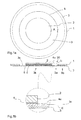
- FIG. 1a is a film frame 1 in this embodiment, at least on an inner circumference 1i circular film frame 1 shown on its underside according to the in FIG. 1b shown sectional view of a film 3 with its adhesive layer 3s is glued concentrically to the film frame 1.
- a product substrate-carrier substrate composite With a radial distance A to the inner periphery 1i of the film frame 1, within the film frame 1, a product substrate-carrier substrate composite is adhered to the adhesive layer 3s of the film 3 concentrically with the film frame 1.
- the product substrate-carrier substrate composite consists of a product substrate 4 adhering to the film 3, a carrier substrate 2, and a bonding layer 6 connecting the product substrate 4 and the carrier substrate 2.
- the diameters of the product substrate 4 and the carrier substrate 2 are substantially identical, while the thickness of the product substrate 4 Product substrate 4 is less than the thickness of the carrier substrate. 2
- the film 3 consists of a ring-shaped fastening section 3b in the present case, in which the film 3 is fixed to the film frame 1. Furthermore, the film 3 consists of a contacting surface portion 3k in which the product substrate 4 is fixable to the adhesive layer 3s of the film 3. Between the attachment portion 3b and the contacting surface portion 3k is a detachment portion 3a arranged, in particular concentric with the attachment portion 3b and the contacting surface portion 3k, which does not have to have an adhesive function, but which has a decisive function according to the invention.
- the detaching portion 3a thus extends from a periphery 4u of the product substrate 4 to the inner periphery 1i of the film frame 1, herein referred to as a radial distance A.
- the ratio between a thickness D of the film frame 1 and the distance A is advantageously at least 1: 2 to 1:50, in particular 1: 5 to 1:25.
- FIG. 1b As shown starting position are the film 3 contacting side of the product substrate 4 and the film. 3 contacting side of the film frame 1 in alignment and arranged in a plane E.
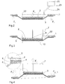
- the in the FIGS. 1a and 1b parts shown are assembled on a known film frame mounter.
- the film 3 and the inner periphery 1i of the film frame 1 form a trough-shaped solvent container 20 in which the product substrate-carrier substrate composite can be arranged as described above.
- solvent shown 22 by introduction means 23 in the solvent container 20 can be introduced.
- the introduction means 23 in the present case consist of a line 24 and a solvent reservoir 25 which can be controlled by a central unit in order to introduce solvent 22 into the solvent container 20.
- the solvent container 20 is variable in volume by the elastic film 3, which is elastic at least in the detachment section 3a, in that a force F s acts on the carrier substrate 2 downward and a force F f acts on the film frame 1.
- the introduction of force is also controlled by a central unit.
- Enlarging the storage tank volume prevents solvent 22 from passing over the edge of the film frame 1, and at the same time, allows rapid distribution or introduction of the solvent 22.
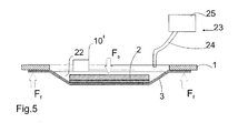
- the force F s is according to FIG. 3 transmitted via a carrier substrate receptacle 7 for receiving the carrier substrate 2, wherein the fixing of the carrier substrate 2 on the carrier substrate receptacle 7 by in the surface of the carrier substrate receptacle 7 incorporated vacuum webs 8th and an attached, not dargschreib vacuum device takes place.
- an acoustic wave generator 10 in particular for generating ultrasonic waves, can be arranged, by which ultrasonic waves can be transmitted to the product substrate 4, but in particular to the bonding layer 6 and the solvent 22, as a result of the process of L Kunststoffs is greatly accelerated, in particular by a factor of 2, preferably by a factor of 5, more preferably by a factor of 10 to 50.
- the sound wave generator 10 is in contact at least with the surface of the fluid solvent 22, but is preferably at least partially immersed therein.
- the sound waves can be transmitted directly to the solvent 22 and from the solvent 22 to the bonding layer 6.
- the force F f acting on the film frame 1 can - as in FIG. 3 shown - evenly distributed as a surface force acting on the film frame 1, so that on the deformation of the film 3 in the detachment section 3a, the change in volume of the solvent container 20 can be effected.
- the force F f1 or a plurality of forces F f1 , F f2 to F fn can / may be introduced at points distributed on the circumference of the film frame 1 or distributed by a film frame recording introduced.
- the receiving device for introducing the force into the film frame 1 a tilting of the film frame 1 must be permitting.
- FIG. 3 illustrated method step of dissolution by the solvent 22 and in FIG. 4 illustrated step of detachment by opposing forces F s , F f1 , F f2 , F fn may be provided a method step by which the solvent 22 is removed from the solvent container 20, in particular by suction.
Landscapes
- Engineering & Computer Science (AREA)
- Computer Hardware Design (AREA)
- Physics & Mathematics (AREA)
- Condensed Matter Physics & Semiconductors (AREA)
- General Physics & Mathematics (AREA)
- Manufacturing & Machinery (AREA)
- Microelectronics & Electronic Packaging (AREA)
- Power Engineering (AREA)
- Mechanical Engineering (AREA)
- Container, Conveyance, Adherence, Positioning, Of Wafer (AREA)
- Laminated Bodies (AREA)
- Application Of Or Painting With Fluid Materials (AREA)
- Mechanical Treatment Of Semiconductor (AREA)
- Adhesives Or Adhesive Processes (AREA)
Claims (14)
- Réservoir à solvant pour dissoudre une couche d'assemblage (6) entre un substrat de produit (4) et un substrat porteur (2) assemblé avec ce dernier, avec les attributs suivants :- un cadre pour un film (1),- un film (3) flexible, relié avec le cadre pour film (1) qui comporte une couche collante (3s) destinée à recevoir le substrat de produit (4), dans une partie de surface de contact (3k) du film (3), le film (3) étant relié avec le cadre pour film (1) dans une partie de fixation (3b) du film (3) entourant la partie de surface de contact (3k), caractérisé en ce que le réservoir à solvant (20) pour recevoir le solvant (22) destiné à dissoudre la couche d'assemblage (6) est formé par le cadre pour film (1) et par le film (3) et en ce que le substrat de produit (4) et la couche d'assemblage (6) peuvent être réceptionnés dans le réservoir à solvant (20).
- Réservoir à solvant (20) selon la revendication 1, qui est conçu avec un volume variable.
- Réservoir à solvant (20) selon l'une quelconque des revendications précédentes qui est conçu de telle sorte qu'au moins au début de l'opération consistant à dissoudre la couche d'assemblage (6), notamment uniquement dans la zone d'une périphérie (4u) du substrat de produit (4), le solvant (22) est conçu en version active.
- Réservoir à solvant (20) selon l'une quelconque des revendications précédentes, caractérisé en ce que le film (3) peut se tendre dans une partie de décollement (3a) située entre la partie de surface de contact (3k) et la partie de fixation (3b), notamment par une force Fs agissant sur le substrat porteur et une force Ff orientée à l'encontre de la force Fs, agissant sur le cadre pour film (1).
- Réservoir à solvant (20) selon l'une quelconque des revendications précédentes lequel est conçu en forme de cuve.
- Procédé destiné à dissoudre une couche d'assemblage (6) entre un substrat de produit (4) et un substrat porteur (2) assemblé avec ce dernier, avec les étapes suivantes :- création d'un réservoir à solvant (20) formé par un cadre pour film (1) et un film (3) flexible relié avec le cadre pour film, destiné à recevoir un solvant (22) pour dissoudre la couche d'assemblage (6),- réception du substrat de produit (4) et de la couche d'assemblage (6) dans le réservoir à solvant (20) et- introduction de solvant (22) dans le réservoir à solvant (20) et décollement de la couche d'assemblage (6).
- Procédé selon la revendication 6, caractérisé en ce qu'après l'introduction du solvant (22) et dissolution au moins partielle de la couche d'assemblage (6), il s'effectue un décollement du substrat de produit (4) du substrat porteur (2) par solvant.
- Procédé selon la revendication 6 ou la revendication 7, caractérisé en ce qu'au moins au début de la dissolution de la couche d'assemblage (6), le solvant (22) agit notamment uniquement dans la zone d'une périphérie (4u) du substrat de produit (4).
- Procédé selon l'une quelconque des revendications 6 à 8, caractérisé en ce que le décollement est provoqué par une force Fs agissant sur le substrat porteur (2) et par une force Ff dirigée à l'encontre de la force Fs et agissant sur le cadre pour film (1).
- Procédé selon l'une quelconque des revendications 6 à 9, caractérisé en ce que le décollement du substrat de produit (4) s'effectue de manière concentrique à partir de la périphérie (4u) du substrat de produit (4) vers le centre (4z) du substrat de produit (4).
- Procédé selon l'une quelconque des revendications 6 à 10, caractérisé en ce qu'on assemble le substrat de produit (4) avec le substrat porteur (2) par l'intermédiaire d'une couche d'assemblage comprenant différentes colles.
- Procédé selon l'une quelconque des revendications 6 à 11, caractérisé en ce que le solvant (22), comprend un produit fluide, dissolvant notamment de manière sélective la couche d'assemblage (6) pour décoller au moins partiellement la couche d'assemblage.
- Procédé selon l'une quelconque des revendications 6 à 12, caractérisé en ce qu'on dissout la couche d'assemblage dans des régions définies.
- Procédé selon l'une quelconque des revendications 6 à 13, caractérisé en ce qu'on dissout l'une des couches précise parmi plusieurs couches d'assemblage.
Priority Applications (1)
| Application Number | Priority Date | Filing Date | Title |
|---|---|---|---|
| EP12179537.1A EP2523208B1 (fr) | 2010-04-23 | 2010-04-23 | Dispositif et procédé de séparation d'un substrat de produit et d'un substrat de support |
Applications Claiming Priority (2)
| Application Number | Priority Date | Filing Date | Title |
|---|---|---|---|
| EP10004313A EP2381464B1 (fr) | 2010-04-23 | 2010-04-23 | Dispositif et procédé de séparation d'un substrat de produit et d'un substrat de support |
| EP12179537.1A EP2523208B1 (fr) | 2010-04-23 | 2010-04-23 | Dispositif et procédé de séparation d'un substrat de produit et d'un substrat de support |
Related Parent Applications (1)
| Application Number | Title | Priority Date | Filing Date |
|---|---|---|---|
| EP10004313.2 Division | 2010-04-23 |
Publications (2)
| Publication Number | Publication Date |
|---|---|
| EP2523208A1 EP2523208A1 (fr) | 2012-11-14 |
| EP2523208B1 true EP2523208B1 (fr) | 2013-06-12 |
Family
ID=42356878
Family Applications (3)
| Application Number | Title | Priority Date | Filing Date |
|---|---|---|---|
| EP12179539.7A Active EP2523209B1 (fr) | 2010-04-23 | 2010-04-23 | Dispositif et procédé de séparation d'un substrat de produit et d'un substrat de support |
| EP12179537.1A Active EP2523208B1 (fr) | 2010-04-23 | 2010-04-23 | Dispositif et procédé de séparation d'un substrat de produit et d'un substrat de support |
| EP10004313A Active EP2381464B1 (fr) | 2010-04-23 | 2010-04-23 | Dispositif et procédé de séparation d'un substrat de produit et d'un substrat de support |
Family Applications Before (1)
| Application Number | Title | Priority Date | Filing Date |
|---|---|---|---|
| EP12179539.7A Active EP2523209B1 (fr) | 2010-04-23 | 2010-04-23 | Dispositif et procédé de séparation d'un substrat de produit et d'un substrat de support |
Family Applications After (1)
| Application Number | Title | Priority Date | Filing Date |
|---|---|---|---|
| EP10004313A Active EP2381464B1 (fr) | 2010-04-23 | 2010-04-23 | Dispositif et procédé de séparation d'un substrat de produit et d'un substrat de support |
Country Status (8)
| Country | Link |
|---|---|
| US (3) | US9272501B2 (fr) |
| EP (3) | EP2523209B1 (fr) |
| JP (4) | JP5623623B2 (fr) |
| KR (3) | KR101454985B1 (fr) |
| CN (2) | CN103219265B (fr) |
| SG (1) | SG183305A1 (fr) |
| TW (3) | TWI421929B (fr) |
| WO (1) | WO2011131283A1 (fr) |
Families Citing this family (19)
| Publication number | Priority date | Publication date | Assignee | Title |
|---|---|---|---|---|
| EP2523209B1 (fr) * | 2010-04-23 | 2017-03-08 | EV Group GmbH | Dispositif et procédé de séparation d'un substrat de produit et d'un substrat de support |
| JP5558191B2 (ja) * | 2010-04-27 | 2014-07-23 | 東京応化工業株式会社 | 剥離装置及び剥離方法 |
| KR102064405B1 (ko) | 2014-02-04 | 2020-01-10 | 삼성디스플레이 주식회사 | 기판 박리 장치 및 그것을 이용한 기판 박리 방법 |
| KR102165162B1 (ko) | 2014-03-12 | 2020-10-14 | 삼성디스플레이 주식회사 | 기판 박리 장치 및 이를 이용한 소자 제조 방법 |
| JP6216727B2 (ja) * | 2014-05-08 | 2017-10-18 | 東京応化工業株式会社 | 支持体分離方法 |
| JP6268483B2 (ja) * | 2014-06-03 | 2018-01-31 | 旭硝子株式会社 | 積層体の剥離装置及び剥離方法並びに電子デバイスの製造方法 |
| SG11201603148VA (en) * | 2014-12-18 | 2016-07-28 | Ev Group E Thallner Gmbh | Method for bonding substrates |
| JP2016146429A (ja) * | 2015-02-09 | 2016-08-12 | トヨタ自動車株式会社 | 半導体装置の製造方法 |
| US10343417B2 (en) * | 2015-07-15 | 2019-07-09 | Hewlett-Packard Development Company, L.P. | Diagnostic plot for printing system |
| CN106053505A (zh) * | 2016-05-17 | 2016-10-26 | 深圳市宁深检验检测技术有限公司 | 一种表面覆膜金片金含量及金质量的快速测定方法 |
| JP7000129B2 (ja) * | 2017-11-15 | 2022-01-19 | 芝浦メカトロニクス株式会社 | 成膜装置 |
| JP6935306B2 (ja) * | 2017-11-16 | 2021-09-15 | 芝浦メカトロニクス株式会社 | 成膜装置 |
| EP3664128B1 (fr) * | 2018-12-06 | 2021-03-31 | Heraeus Deutschland GmbH & Co. KG | Unité d'emballage pour substrats |
| JP7146354B2 (ja) | 2019-01-22 | 2022-10-04 | 株式会社ディスコ | キャリア板の除去方法 |
| KR102191204B1 (ko) * | 2019-07-31 | 2020-12-15 | 삼영공업 주식회사 | 접합판 분리 장치 및 접합판 분리 방법 |
| JP7262903B2 (ja) * | 2019-08-26 | 2023-04-24 | 株式会社ディスコ | キャリア板の除去方法 |
| JP7262904B2 (ja) * | 2019-08-26 | 2023-04-24 | 株式会社ディスコ | キャリア板の除去方法 |
| KR102298227B1 (ko) * | 2019-08-30 | 2021-09-06 | 주식회사 엘트린 | 디본딩 장치. |
| JP7511980B2 (ja) * | 2020-07-21 | 2024-07-08 | 株式会社ディスコ | キャリア板の除去方法 |
Family Cites Families (60)
| Publication number | Priority date | Publication date | Assignee | Title |
|---|---|---|---|---|
| US3988196A (en) | 1967-10-09 | 1976-10-26 | Western Electric Company, Inc. | Apparatus for transferring an oriented array of articles |
| US4826553A (en) * | 1987-06-18 | 1989-05-02 | The United States Of America As Represented By The Secretary Of The Air Force | Method for replicating an optical element |
| US5273615A (en) | 1992-04-06 | 1993-12-28 | Motorola, Inc. | Apparatus and method for handling fragile semiconductor wafers |
| JPH06275717A (ja) * | 1993-01-22 | 1994-09-30 | Mitsubishi Electric Corp | ウエハはがし方法 |
| JPH06268051A (ja) | 1993-03-10 | 1994-09-22 | Mitsubishi Electric Corp | ウエハ剥し装置 |
| JP4220580B2 (ja) | 1995-02-10 | 2009-02-04 | 三菱電機株式会社 | 半導体装置の製造装置 |
| JP3407835B2 (ja) | 1995-03-09 | 2003-05-19 | 東京応化工業株式会社 | 基板端縁部被膜の除去方法及び除去装置 |
| US6342434B1 (en) * | 1995-12-04 | 2002-01-29 | Hitachi, Ltd. | Methods of processing semiconductor wafer, and producing IC card, and carrier |
| JP2004119975A (ja) * | 1995-12-04 | 2004-04-15 | Renesas Technology Corp | Icカードの製造方法 |
| DE19734635A1 (de) | 1997-08-11 | 1999-02-18 | Gen Semiconductor Ireland Macr | Verfahren und Vorrichtung zum Ablösen von Bauelementen von einer Folie |
| US6090687A (en) | 1998-07-29 | 2000-07-18 | Agilent Technolgies, Inc. | System and method for bonding and sealing microfabricated wafers to form a single structure having a vacuum chamber therein |
| JP2001196404A (ja) | 2000-01-11 | 2001-07-19 | Fujitsu Ltd | 半導体装置及びその製造方法 |
| JP3768069B2 (ja) | 2000-05-16 | 2006-04-19 | 信越半導体株式会社 | 半導体ウエーハの薄型化方法 |
| DE10048881A1 (de) | 2000-09-29 | 2002-03-07 | Infineon Technologies Ag | Vorrichtung und Verfahren zum planen Verbinden zweier Wafer für ein Dünnschleifen und ein Trennen eines Produkt-Wafers |
| US6713880B2 (en) | 2001-02-07 | 2004-03-30 | Matsushita Electric Industrial Co., Ltd. | Semiconductor device and method for producing the same, and method for mounting semiconductor device |
| JP2002237515A (ja) | 2001-02-07 | 2002-08-23 | Mitsubishi Gas Chem Co Inc | 薄葉化半導体基板の剥離装置および剥離法 |
| DE10108369A1 (de) | 2001-02-21 | 2002-08-29 | B L E Lab Equipment Gmbh | Verfahren und Vorrichtung zum Ablösen eines Halbleiterwafers von einem Träger |
| AT502233B1 (de) | 2001-06-07 | 2007-04-15 | Thallner Erich | Vorrichtung zum lösen eines trägers von einer halbleiterscheibe |
| MXPA04001781A (es) | 2002-03-27 | 2004-06-24 | Matsushita Electric Ind Co Ltd | Metodo para fabricacion de medio de grabacion optica de informacion en capas multiples. |
| JP4271409B2 (ja) * | 2002-05-22 | 2009-06-03 | リンテック株式会社 | 脆質材料の加工方法 |
| TWI258316B (en) | 2002-10-25 | 2006-07-11 | Ritdisplay Corp | FPD encapsulation apparatus and method for encapsulating ehereof |
| JP2004193237A (ja) | 2002-12-10 | 2004-07-08 | Disco Abrasive Syst Ltd | 粘着シートを具備するウェハー保持部材,及び粘着シートの剥離方法 |
| US7187162B2 (en) * | 2002-12-16 | 2007-03-06 | S.O.I.Tec Silicon On Insulator Technologies S.A. | Tools and methods for disuniting semiconductor wafers |
| JP4364535B2 (ja) | 2003-03-27 | 2009-11-18 | シャープ株式会社 | 半導体装置の製造方法 |
| JP4474854B2 (ja) | 2003-07-02 | 2010-06-09 | Jsr株式会社 | 感放射線性接着剤組成物およびこれを用いたウェハーの加工方法 |
| DE10340409B4 (de) | 2003-09-02 | 2007-05-24 | Fraunhofer-Gesellschaft zur Förderung der angewandten Forschung e.V. | Trägerwafer und Verfahren zum Bearbeiten eines Halbleiterwafers unter Verwendung eines Trägerwafers |
| JP3912350B2 (ja) * | 2003-09-22 | 2007-05-09 | 住友電気工業株式会社 | 半導体装置の製造方法 |
| JP4447280B2 (ja) | 2003-10-16 | 2010-04-07 | リンテック株式会社 | 表面保護用シートおよび半導体ウエハの研削方法 |
| JP2005191535A (ja) * | 2003-12-01 | 2005-07-14 | Tokyo Ohka Kogyo Co Ltd | 貼り付け装置および貼り付け方法 |
| JP2006135272A (ja) * | 2003-12-01 | 2006-05-25 | Tokyo Ohka Kogyo Co Ltd | 基板のサポートプレート及びサポートプレートの剥離方法 |
| DE102004018250A1 (de) | 2004-04-15 | 2005-11-03 | Infineon Technologies Ag | Wafer-Stabilisierungsvorrichtung und Verfahren zu dessen Herstellung |
| JP2005353859A (ja) | 2004-06-11 | 2005-12-22 | Taiyo Yuden Co Ltd | 半導体ウェハの剥離方法 |
| US7829152B2 (en) | 2006-10-05 | 2010-11-09 | Lam Research Corporation | Electroless plating method and apparatus |
| JP2006032506A (ja) | 2004-07-14 | 2006-02-02 | Taiyo Yuden Co Ltd | 半導体ウェハの剥離方法および剥離装置 |
| JP2006059861A (ja) * | 2004-08-17 | 2006-03-02 | Lintec Corp | 脆質部材の転着装置 |
| JP4679890B2 (ja) | 2004-11-29 | 2011-05-11 | 東京応化工業株式会社 | サポートプレートの貼り付け装置 |
| TWI413152B (zh) * | 2005-03-01 | 2013-10-21 | Semiconductor Energy Lab | 半導體裝置製造方法 |
| JP4748518B2 (ja) * | 2005-07-20 | 2011-08-17 | 古河電気工業株式会社 | ダイシングダイボンドテープおよびダイシングテープ |
| JP4848153B2 (ja) | 2005-08-10 | 2011-12-28 | ルネサスエレクトロニクス株式会社 | 半導体装置の製造方法 |
| JP4721828B2 (ja) * | 2005-08-31 | 2011-07-13 | 東京応化工業株式会社 | サポートプレートの剥離方法 |
| TW200730414A (en) * | 2005-11-18 | 2007-08-16 | Advanced Tech Materials | Material storage and dispensing containers and systems comprising same |
| JP4668052B2 (ja) | 2005-12-06 | 2011-04-13 | 東京応化工業株式会社 | 剥離装置 |
| DE102006000687B4 (de) | 2006-01-03 | 2010-09-09 | Thallner, Erich, Dipl.-Ing. | Kombination aus einem Träger und einem Wafer, Vorrichtung zum Trennen der Kombination und Verfahren zur Handhabung eines Trägers und eines Wafers |
| JP2008021929A (ja) * | 2006-07-14 | 2008-01-31 | Tokyo Ohka Kogyo Co Ltd | サポートプレート、搬送装置、剥離装置及び剥離方法 |
| JP5027460B2 (ja) * | 2006-07-28 | 2012-09-19 | 東京応化工業株式会社 | ウエハの接着方法、薄板化方法、及び剥離方法 |
| JP4847255B2 (ja) | 2006-08-30 | 2011-12-28 | 株式会社テオス | 半導体ウエーハの加工方法 |
| JP4402144B2 (ja) | 2006-09-29 | 2010-01-20 | 株式会社半導体エネルギー研究所 | 半導体装置の作製方法 |
| JP5238927B2 (ja) * | 2007-03-14 | 2013-07-17 | セミコンダクター・コンポーネンツ・インダストリーズ・リミテッド・ライアビリティ・カンパニー | 半導体装置の製造方法 |
| JP4958287B2 (ja) | 2007-05-30 | 2012-06-20 | 東京応化工業株式会社 | 剥がし装置における剥離方法 |
| JP5090789B2 (ja) | 2007-05-30 | 2012-12-05 | 東京応化工業株式会社 | 貼り合わせ装置、接着剤の溶解を防ぐ方法、及び貼り合わせ方法 |
| US20090017323A1 (en) | 2007-07-13 | 2009-01-15 | 3M Innovative Properties Company | Layered body and method for manufacturing thin substrate using the layered body |
| JP5074940B2 (ja) * | 2008-01-30 | 2012-11-14 | 東京応化工業株式会社 | 基板の処理方法 |
| JP2009182256A (ja) | 2008-01-31 | 2009-08-13 | Tokyo Ohka Kogyo Co Ltd | 基板の処理装置および基板の処理方法 |
| JP4965485B2 (ja) | 2008-02-29 | 2012-07-04 | 東京応化工業株式会社 | 処理液浸透ユニットおよび処理装置 |
| JP2010027720A (ja) | 2008-07-16 | 2010-02-04 | Shin Etsu Polymer Co Ltd | リングフレーム |
| WO2010023935A1 (fr) * | 2008-08-29 | 2010-03-04 | 株式会社ニコン | Dispositif et procédé d'alignement de substrats, et procédé de fabrication de semi-conducteur multicouche |
| TWM355799U (en) * | 2008-09-16 | 2009-05-01 | Ye Siang Entpr Co Ltd | Disassembling and assembling jig |
| EP2230683B1 (fr) | 2009-03-18 | 2016-03-16 | EV Group GmbH | Dispositif et procédé de séparation d'une tranche de silicium à partir d'un support |
| EP2523209B1 (fr) * | 2010-04-23 | 2017-03-08 | EV Group GmbH | Dispositif et procédé de séparation d'un substrat de produit et d'un substrat de support |
| CN104247068B (zh) * | 2012-04-23 | 2017-12-05 | 南洋理工大学 | 用于分离多层结构的装置和方法 |
-
2010
- 2010-04-23 EP EP12179539.7A patent/EP2523209B1/fr active Active
- 2010-04-23 EP EP12179537.1A patent/EP2523208B1/fr active Active
- 2010-04-23 EP EP10004313A patent/EP2381464B1/fr active Active
-
2011
- 2011-03-29 CN CN201310126332.XA patent/CN103219265B/zh active Active
- 2011-03-29 US US13/641,479 patent/US9272501B2/en active Active
- 2011-03-29 SG SG2012060018A patent/SG183305A1/en unknown
- 2011-03-29 WO PCT/EP2011/001556 patent/WO2011131283A1/fr active Application Filing
- 2011-03-29 JP JP2013504150A patent/JP5623623B2/ja active Active
- 2011-03-29 KR KR1020127032468A patent/KR101454985B1/ko active IP Right Grant
- 2011-03-29 KR KR1020127032469A patent/KR101742347B1/ko active IP Right Grant
- 2011-03-29 KR KR1020127022017A patent/KR101476516B1/ko active IP Right Grant
- 2011-03-29 CN CN201180011757.5A patent/CN103620732B/zh active Active
- 2011-04-22 TW TW100114153A patent/TWI421929B/zh active
- 2011-04-22 TW TW101145179A patent/TWI447793B/zh active
- 2011-04-22 TW TW101145174A patent/TWI520198B/zh active
-
2013
- 2013-05-10 JP JP2013099954A patent/JP5714053B2/ja active Active
- 2013-06-18 US US13/920,458 patent/US9381729B2/en active Active
-
2014
- 2014-07-28 JP JP2014152881A patent/JP5997732B2/ja active Active
-
2015
- 2015-04-13 JP JP2015081502A patent/JP6099688B2/ja active Active
- 2015-05-19 US US14/715,691 patent/US9457552B2/en active Active
Also Published As
Similar Documents
| Publication | Publication Date | Title |
|---|---|---|
| EP2523208B1 (fr) | Dispositif et procédé de séparation d'un substrat de produit et d'un substrat de support | |
| EP2290679B1 (fr) | Dispositif et procédé de séparation d'un substrat de produit (par exemple, d'une tranche semi-conductrice) d'un substrat de support par déformation d'un film flexible monté sur un cadre | |
| EP2382656B1 (fr) | Procédé de séparation pour système stratifié comprenant une tranche | |
| EP2230683B1 (fr) | Dispositif et procédé de séparation d'une tranche de silicium à partir d'un support | |
| DE112013000980B4 (de) | Verfahren zum temporären Verbinden eines Produktsubstrats mit einem Trägersubstrat sowie ein entsprechender Verbund | |
| DE10260233B4 (de) | Verfahren zum Befestigen eines Werkstücks mit einem Feststoff an einem Werkstückträger und Werkstückträger | |
| DE112009000140T5 (de) | Verfahren zum reversiblen Anbringen eines Vorrichtungswafers an einem Trägersubstrat | |
| DE102009018156B4 (de) | Vorrichtung und Verfahren zum Trennen eines Substrats von einem Trägersubstrat | |
| AT502233A1 (de) | Vorrichtung zum lösen eines trägers von einer halbleiterscheibe | |
| WO2012097830A1 (fr) | Procédé servant à détacher un substrat produit d'un substrat support | |
| EP2553719B1 (fr) | Procédé de fabrication d'une tranche pourvue de puces à l'aide de deux tranches de support séparémment détachables avec des couches annulaires d'adhésion à différentes largeurs d'anneau | |
| DE102014202842B4 (de) | Verfahren zum Herstellen eines mikromechanischen Bauteils | |
| WO2004032593A2 (fr) | Porte-substrat mince | |
| DE102004004476B3 (de) | Verfahren zum Aufbringen von Deckelstrukturen mittels eines biegsamen Trägers | |
| DE4223215C2 (de) | Verfahren zur Bearbeitung von Siliziumwafern | |
| DE102006048800B4 (de) | Mehrlagenschichtsystem mit hartem Träger zum Trägern von dünnen Wafern bei der Halbleiterherstellung | |
| DE10337920A1 (de) | Verfahren zur Herstellung von Bauteilen | |
| DE102006004834B4 (de) | Verfahren zum Behandeln von Wafern beim Abdünnen | |
| AT517638B1 (de) | Aufnahmeeinrichtung zur Handhabung strukturierter Substrate | |
| DE102020210751A1 (de) | Verfahren zum entfernen einer trägerplatte | |
| AT411197B (de) | Verfahren zum montieren, haltern oder abmontieren eines wafers sowie einrichtung zur durchführung des verfahrens | |
| DE10262317B4 (de) | Verfahren zum Trennen eines Werkstücks von einem Werkstückträger |
Legal Events
| Date | Code | Title | Description |
|---|---|---|---|
| PUAI | Public reference made under article 153(3) epc to a published international application that has entered the european phase |
Free format text: ORIGINAL CODE: 0009012 |
|
| 17P | Request for examination filed |
Effective date: 20121001 |
|
| AC | Divisional application: reference to earlier application |
Ref document number: 2381464 Country of ref document: EP Kind code of ref document: P |
|
| AK | Designated contracting states |
Kind code of ref document: A1 Designated state(s): AT BE BG CH CY CZ DE DK EE ES FI FR GB GR HR HU IE IS IT LI LT LU LV MC MK MT NL NO PL PT RO SE SI SK SM TR |
|
| GRAP | Despatch of communication of intention to grant a patent |
Free format text: ORIGINAL CODE: EPIDOSNIGR1 |
|
| GRAS | Grant fee paid |
Free format text: ORIGINAL CODE: EPIDOSNIGR3 |
|
| GRAA | (expected) grant |
Free format text: ORIGINAL CODE: 0009210 |
|
| AC | Divisional application: reference to earlier application |
Ref document number: 2381464 Country of ref document: EP Kind code of ref document: P |
|
| AK | Designated contracting states |
Kind code of ref document: B1 Designated state(s): AT BE BG CH CY CZ DE DK EE ES FI FR GB GR HR HU IE IS IT LI LT LU LV MC MK MT NL NO PL PT RO SE SI SK SM TR |
|
| REG | Reference to a national code |
Ref country code: GB Ref legal event code: FG4D Free format text: NOT ENGLISH |
|
| REG | Reference to a national code |
Ref country code: CH Ref legal event code: EP |
|
| REG | Reference to a national code |
Ref country code: AT Ref legal event code: REF Ref document number: 616960 Country of ref document: AT Kind code of ref document: T Effective date: 20130615 |
|
| REG | Reference to a national code |
Ref country code: IE Ref legal event code: FG4D Free format text: LANGUAGE OF EP DOCUMENT: GERMAN |
|
| REG | Reference to a national code |
Ref country code: DE Ref legal event code: R096 Ref document number: 502010003679 Country of ref document: DE Effective date: 20130808 |
|
| PG25 | Lapsed in a contracting state [announced via postgrant information from national office to epo] |
Ref country code: SI Free format text: LAPSE BECAUSE OF FAILURE TO SUBMIT A TRANSLATION OF THE DESCRIPTION OR TO PAY THE FEE WITHIN THE PRESCRIBED TIME-LIMIT Effective date: 20130612 Ref country code: LT Free format text: LAPSE BECAUSE OF FAILURE TO SUBMIT A TRANSLATION OF THE DESCRIPTION OR TO PAY THE FEE WITHIN THE PRESCRIBED TIME-LIMIT Effective date: 20130612 Ref country code: ES Free format text: LAPSE BECAUSE OF FAILURE TO SUBMIT A TRANSLATION OF THE DESCRIPTION OR TO PAY THE FEE WITHIN THE PRESCRIBED TIME-LIMIT Effective date: 20130923 Ref country code: FI Free format text: LAPSE BECAUSE OF FAILURE TO SUBMIT A TRANSLATION OF THE DESCRIPTION OR TO PAY THE FEE WITHIN THE PRESCRIBED TIME-LIMIT Effective date: 20130612 Ref country code: SE Free format text: LAPSE BECAUSE OF FAILURE TO SUBMIT A TRANSLATION OF THE DESCRIPTION OR TO PAY THE FEE WITHIN THE PRESCRIBED TIME-LIMIT Effective date: 20130612 Ref country code: GR Free format text: LAPSE BECAUSE OF FAILURE TO SUBMIT A TRANSLATION OF THE DESCRIPTION OR TO PAY THE FEE WITHIN THE PRESCRIBED TIME-LIMIT Effective date: 20130913 Ref country code: NO Free format text: LAPSE BECAUSE OF FAILURE TO SUBMIT A TRANSLATION OF THE DESCRIPTION OR TO PAY THE FEE WITHIN THE PRESCRIBED TIME-LIMIT Effective date: 20130912 |
|
| REG | Reference to a national code |
Ref country code: NL Ref legal event code: VDEP Effective date: 20130612 |
|
| REG | Reference to a national code |
Ref country code: LT Ref legal event code: MG4D |
|
| PG25 | Lapsed in a contracting state [announced via postgrant information from national office to epo] |
Ref country code: HR Free format text: LAPSE BECAUSE OF FAILURE TO SUBMIT A TRANSLATION OF THE DESCRIPTION OR TO PAY THE FEE WITHIN THE PRESCRIBED TIME-LIMIT Effective date: 20130612 Ref country code: BG Free format text: LAPSE BECAUSE OF FAILURE TO SUBMIT A TRANSLATION OF THE DESCRIPTION OR TO PAY THE FEE WITHIN THE PRESCRIBED TIME-LIMIT Effective date: 20130912 |
|
| PG25 | Lapsed in a contracting state [announced via postgrant information from national office to epo] |
Ref country code: LV Free format text: LAPSE BECAUSE OF FAILURE TO SUBMIT A TRANSLATION OF THE DESCRIPTION OR TO PAY THE FEE WITHIN THE PRESCRIBED TIME-LIMIT Effective date: 20130612 |
|
| PG25 | Lapsed in a contracting state [announced via postgrant information from national office to epo] |
Ref country code: IS Free format text: LAPSE BECAUSE OF FAILURE TO SUBMIT A TRANSLATION OF THE DESCRIPTION OR TO PAY THE FEE WITHIN THE PRESCRIBED TIME-LIMIT Effective date: 20131012 Ref country code: CZ Free format text: LAPSE BECAUSE OF FAILURE TO SUBMIT A TRANSLATION OF THE DESCRIPTION OR TO PAY THE FEE WITHIN THE PRESCRIBED TIME-LIMIT Effective date: 20130612 Ref country code: PT Free format text: LAPSE BECAUSE OF FAILURE TO SUBMIT A TRANSLATION OF THE DESCRIPTION OR TO PAY THE FEE WITHIN THE PRESCRIBED TIME-LIMIT Effective date: 20131014 Ref country code: EE Free format text: LAPSE BECAUSE OF FAILURE TO SUBMIT A TRANSLATION OF THE DESCRIPTION OR TO PAY THE FEE WITHIN THE PRESCRIBED TIME-LIMIT Effective date: 20130612 Ref country code: SK Free format text: LAPSE BECAUSE OF FAILURE TO SUBMIT A TRANSLATION OF THE DESCRIPTION OR TO PAY THE FEE WITHIN THE PRESCRIBED TIME-LIMIT Effective date: 20130612 |
|
| PG25 | Lapsed in a contracting state [announced via postgrant information from national office to epo] |
Ref country code: NL Free format text: LAPSE BECAUSE OF FAILURE TO SUBMIT A TRANSLATION OF THE DESCRIPTION OR TO PAY THE FEE WITHIN THE PRESCRIBED TIME-LIMIT Effective date: 20130612 Ref country code: PL Free format text: LAPSE BECAUSE OF FAILURE TO SUBMIT A TRANSLATION OF THE DESCRIPTION OR TO PAY THE FEE WITHIN THE PRESCRIBED TIME-LIMIT Effective date: 20130612 Ref country code: RO Free format text: LAPSE BECAUSE OF FAILURE TO SUBMIT A TRANSLATION OF THE DESCRIPTION OR TO PAY THE FEE WITHIN THE PRESCRIBED TIME-LIMIT Effective date: 20130612 |
|
| PLBE | No opposition filed within time limit |
Free format text: ORIGINAL CODE: 0009261 |
|
| STAA | Information on the status of an ep patent application or granted ep patent |
Free format text: STATUS: NO OPPOSITION FILED WITHIN TIME LIMIT |
|
| PG25 | Lapsed in a contracting state [announced via postgrant information from national office to epo] |
Ref country code: DK Free format text: LAPSE BECAUSE OF FAILURE TO SUBMIT A TRANSLATION OF THE DESCRIPTION OR TO PAY THE FEE WITHIN THE PRESCRIBED TIME-LIMIT Effective date: 20130612 |
|
| 26N | No opposition filed |
Effective date: 20140313 |
|
| PG25 | Lapsed in a contracting state [announced via postgrant information from national office to epo] |
Ref country code: IT Free format text: LAPSE BECAUSE OF FAILURE TO SUBMIT A TRANSLATION OF THE DESCRIPTION OR TO PAY THE FEE WITHIN THE PRESCRIBED TIME-LIMIT Effective date: 20130612 |
|
| REG | Reference to a national code |
Ref country code: DE Ref legal event code: R097 Ref document number: 502010003679 Country of ref document: DE Effective date: 20140313 |
|
| PG25 | Lapsed in a contracting state [announced via postgrant information from national office to epo] |
Ref country code: MC Free format text: LAPSE BECAUSE OF FAILURE TO SUBMIT A TRANSLATION OF THE DESCRIPTION OR TO PAY THE FEE WITHIN THE PRESCRIBED TIME-LIMIT Effective date: 20130612 Ref country code: LU Free format text: LAPSE BECAUSE OF FAILURE TO SUBMIT A TRANSLATION OF THE DESCRIPTION OR TO PAY THE FEE WITHIN THE PRESCRIBED TIME-LIMIT Effective date: 20140423 |
|
| REG | Reference to a national code |
Ref country code: CH Ref legal event code: PL |
|
| REG | Reference to a national code |
Ref country code: IE Ref legal event code: MM4A |
|
| PG25 | Lapsed in a contracting state [announced via postgrant information from national office to epo] |
Ref country code: CH Free format text: LAPSE BECAUSE OF NON-PAYMENT OF DUE FEES Effective date: 20140430 Ref country code: LI Free format text: LAPSE BECAUSE OF NON-PAYMENT OF DUE FEES Effective date: 20140430 |
|
| PG25 | Lapsed in a contracting state [announced via postgrant information from national office to epo] |
Ref country code: IE Free format text: LAPSE BECAUSE OF NON-PAYMENT OF DUE FEES Effective date: 20140423 |
|
| PG25 | Lapsed in a contracting state [announced via postgrant information from national office to epo] |
Ref country code: MT Free format text: LAPSE BECAUSE OF FAILURE TO SUBMIT A TRANSLATION OF THE DESCRIPTION OR TO PAY THE FEE WITHIN THE PRESCRIBED TIME-LIMIT Effective date: 20130612 |
|
| REG | Reference to a national code |
Ref country code: FR Ref legal event code: PLFP Year of fee payment: 7 |
|
| PG25 | Lapsed in a contracting state [announced via postgrant information from national office to epo] |
Ref country code: SM Free format text: LAPSE BECAUSE OF FAILURE TO SUBMIT A TRANSLATION OF THE DESCRIPTION OR TO PAY THE FEE WITHIN THE PRESCRIBED TIME-LIMIT Effective date: 20130612 |
|
| PG25 | Lapsed in a contracting state [announced via postgrant information from national office to epo] |
Ref country code: CY Free format text: LAPSE BECAUSE OF FAILURE TO SUBMIT A TRANSLATION OF THE DESCRIPTION OR TO PAY THE FEE WITHIN THE PRESCRIBED TIME-LIMIT Effective date: 20130612 |
|
| PG25 | Lapsed in a contracting state [announced via postgrant information from national office to epo] |
Ref country code: HU Free format text: LAPSE BECAUSE OF FAILURE TO SUBMIT A TRANSLATION OF THE DESCRIPTION OR TO PAY THE FEE WITHIN THE PRESCRIBED TIME-LIMIT; INVALID AB INITIO Effective date: 20100423 Ref country code: BE Free format text: LAPSE BECAUSE OF FAILURE TO SUBMIT A TRANSLATION OF THE DESCRIPTION OR TO PAY THE FEE WITHIN THE PRESCRIBED TIME-LIMIT Effective date: 20140430 Ref country code: TR Free format text: LAPSE BECAUSE OF FAILURE TO SUBMIT A TRANSLATION OF THE DESCRIPTION OR TO PAY THE FEE WITHIN THE PRESCRIBED TIME-LIMIT Effective date: 20130612 |
|
| REG | Reference to a national code |
Ref country code: FR Ref legal event code: PLFP Year of fee payment: 8 |
|
| REG | Reference to a national code |
Ref country code: FR Ref legal event code: PLFP Year of fee payment: 9 |
|
| PG25 | Lapsed in a contracting state [announced via postgrant information from national office to epo] |
Ref country code: MK Free format text: LAPSE BECAUSE OF FAILURE TO SUBMIT A TRANSLATION OF THE DESCRIPTION OR TO PAY THE FEE WITHIN THE PRESCRIBED TIME-LIMIT Effective date: 20130612 |
|
| PGFP | Annual fee paid to national office [announced via postgrant information from national office to epo] |
Ref country code: GB Payment date: 20240423 Year of fee payment: 15 |
|
| PGFP | Annual fee paid to national office [announced via postgrant information from national office to epo] |
Ref country code: DE Payment date: 20240418 Year of fee payment: 15 |
|
| PGFP | Annual fee paid to national office [announced via postgrant information from national office to epo] |
Ref country code: AT Payment date: 20240417 Year of fee payment: 15 |
|
| PGFP | Annual fee paid to national office [announced via postgrant information from national office to epo] |
Ref country code: FR Payment date: 20240422 Year of fee payment: 15 |