EP2523209B1 - Device and method for releasing a product substrate from a holder substrate - Google Patents
Device and method for releasing a product substrate from a holder substrate Download PDFInfo
- Publication number
- EP2523209B1 EP2523209B1 EP12179539.7A EP12179539A EP2523209B1 EP 2523209 B1 EP2523209 B1 EP 2523209B1 EP 12179539 A EP12179539 A EP 12179539A EP 2523209 B1 EP2523209 B1 EP 2523209B1
- Authority
- EP
- European Patent Office
- Prior art keywords
- product substrate
- film
- substrate
- product
- solvent
- Prior art date
- Legal status (The legal status is an assumption and is not a legal conclusion. Google has not performed a legal analysis and makes no representation as to the accuracy of the status listed.)
- Active
Links
- 239000000758 substrate Substances 0.000 title claims description 96
- 238000000034 method Methods 0.000 title claims description 21
- 239000010410 layer Substances 0.000 claims description 20
- 239000000853 adhesive Substances 0.000 claims description 7
- 230000001070 adhesive effect Effects 0.000 claims description 7
- 239000012790 adhesive layer Substances 0.000 claims description 6
- 239000000047 product Substances 0.000 description 44
- 239000002904 solvent Substances 0.000 description 40
- 238000004090 dissolution Methods 0.000 description 7
- 239000002131 composite material Substances 0.000 description 5
- 235000012431 wafers Nutrition 0.000 description 5
- 239000012876 carrier material Substances 0.000 description 2
- 239000012530 fluid Substances 0.000 description 2
- 238000010438 heat treatment Methods 0.000 description 2
- 239000000463 material Substances 0.000 description 2
- 239000004065 semiconductor Substances 0.000 description 2
- 239000000126 substance Substances 0.000 description 2
- XUIMIQQOPSSXEZ-UHFFFAOYSA-N Silicon Chemical compound [Si] XUIMIQQOPSSXEZ-UHFFFAOYSA-N 0.000 description 1
- 239000004809 Teflon Substances 0.000 description 1
- 229920006362 Teflon® Polymers 0.000 description 1
- 239000006227 byproduct Substances 0.000 description 1
- 238000011161 development Methods 0.000 description 1
- 230000018109 developmental process Effects 0.000 description 1
- 229920002313 fluoropolymer Polymers 0.000 description 1
- 239000004811 fluoropolymer Substances 0.000 description 1
- 239000011521 glass Substances 0.000 description 1
- 238000007654 immersion Methods 0.000 description 1
- 238000003780 insertion Methods 0.000 description 1
- 230000037431 insertion Effects 0.000 description 1
- 238000000926 separation method Methods 0.000 description 1
- 229910052710 silicon Inorganic materials 0.000 description 1
- 239000010703 silicon Substances 0.000 description 1
- 229920001169 thermoplastic Polymers 0.000 description 1
- 239000004416 thermosoftening plastic Substances 0.000 description 1
Images
Classifications
-
- H—ELECTRICITY
- H01—ELECTRIC ELEMENTS
- H01L—SEMICONDUCTOR DEVICES NOT COVERED BY CLASS H10
- H01L21/00—Processes or apparatus adapted for the manufacture or treatment of semiconductor or solid state devices or of parts thereof
- H01L21/67—Apparatus specially adapted for handling semiconductor or electric solid state devices during manufacture or treatment thereof; Apparatus specially adapted for handling wafers during manufacture or treatment of semiconductor or electric solid state devices or components ; Apparatus not specifically provided for elsewhere
- H01L21/67005—Apparatus not specifically provided for elsewhere
- H01L21/67011—Apparatus for manufacture or treatment
- H01L21/67092—Apparatus for mechanical treatment
-
- B—PERFORMING OPERATIONS; TRANSPORTING
- B32—LAYERED PRODUCTS
- B32B—LAYERED PRODUCTS, i.e. PRODUCTS BUILT-UP OF STRATA OF FLAT OR NON-FLAT, e.g. CELLULAR OR HONEYCOMB, FORM
- B32B38/00—Ancillary operations in connection with laminating processes
- B32B38/10—Removing layers, or parts of layers, mechanically or chemically
-
- H—ELECTRICITY
- H01—ELECTRIC ELEMENTS
- H01L—SEMICONDUCTOR DEVICES NOT COVERED BY CLASS H10
- H01L21/00—Processes or apparatus adapted for the manufacture or treatment of semiconductor or solid state devices or of parts thereof
- H01L21/02—Manufacture or treatment of semiconductor devices or of parts thereof
-
- B—PERFORMING OPERATIONS; TRANSPORTING
- B32—LAYERED PRODUCTS
- B32B—LAYERED PRODUCTS, i.e. PRODUCTS BUILT-UP OF STRATA OF FLAT OR NON-FLAT, e.g. CELLULAR OR HONEYCOMB, FORM
- B32B37/00—Methods or apparatus for laminating, e.g. by curing or by ultrasonic bonding
- B32B37/02—Methods or apparatus for laminating, e.g. by curing or by ultrasonic bonding characterised by a sequence of laminating steps, e.g. by adding new layers at consecutive laminating stations
- B32B37/025—Transfer laminating
-
- H—ELECTRICITY
- H01—ELECTRIC ELEMENTS
- H01L—SEMICONDUCTOR DEVICES NOT COVERED BY CLASS H10
- H01L21/00—Processes or apparatus adapted for the manufacture or treatment of semiconductor or solid state devices or of parts thereof
- H01L21/67—Apparatus specially adapted for handling semiconductor or electric solid state devices during manufacture or treatment thereof; Apparatus specially adapted for handling wafers during manufacture or treatment of semiconductor or electric solid state devices or components ; Apparatus not specifically provided for elsewhere
- H01L21/67005—Apparatus not specifically provided for elsewhere
- H01L21/67011—Apparatus for manufacture or treatment
- H01L21/67132—Apparatus for placing on an insulating substrate, e.g. tape
-
- H—ELECTRICITY
- H01—ELECTRIC ELEMENTS
- H01L—SEMICONDUCTOR DEVICES NOT COVERED BY CLASS H10
- H01L21/00—Processes or apparatus adapted for the manufacture or treatment of semiconductor or solid state devices or of parts thereof
- H01L21/67—Apparatus specially adapted for handling semiconductor or electric solid state devices during manufacture or treatment thereof; Apparatus specially adapted for handling wafers during manufacture or treatment of semiconductor or electric solid state devices or components ; Apparatus not specifically provided for elsewhere
- H01L21/67005—Apparatus not specifically provided for elsewhere
- H01L21/67011—Apparatus for manufacture or treatment
- H01L21/6715—Apparatus for applying a liquid, a resin, an ink or the like
-
- H—ELECTRICITY
- H01—ELECTRIC ELEMENTS
- H01L—SEMICONDUCTOR DEVICES NOT COVERED BY CLASS H10
- H01L21/00—Processes or apparatus adapted for the manufacture or treatment of semiconductor or solid state devices or of parts thereof
- H01L21/67—Apparatus specially adapted for handling semiconductor or electric solid state devices during manufacture or treatment thereof; Apparatus specially adapted for handling wafers during manufacture or treatment of semiconductor or electric solid state devices or components ; Apparatus not specifically provided for elsewhere
- H01L21/677—Apparatus specially adapted for handling semiconductor or electric solid state devices during manufacture or treatment thereof; Apparatus specially adapted for handling wafers during manufacture or treatment of semiconductor or electric solid state devices or components ; Apparatus not specifically provided for elsewhere for conveying, e.g. between different workstations
-
- B—PERFORMING OPERATIONS; TRANSPORTING
- B32—LAYERED PRODUCTS
- B32B—LAYERED PRODUCTS, i.e. PRODUCTS BUILT-UP OF STRATA OF FLAT OR NON-FLAT, e.g. CELLULAR OR HONEYCOMB, FORM
- B32B38/00—Ancillary operations in connection with laminating processes
- B32B2038/0052—Other operations not otherwise provided for
-
- B—PERFORMING OPERATIONS; TRANSPORTING
- B32—LAYERED PRODUCTS
- B32B—LAYERED PRODUCTS, i.e. PRODUCTS BUILT-UP OF STRATA OF FLAT OR NON-FLAT, e.g. CELLULAR OR HONEYCOMB, FORM
- B32B2307/00—Properties of the layers or laminate
- B32B2307/50—Properties of the layers or laminate having particular mechanical properties
- B32B2307/546—Flexural strength; Flexion stiffness
-
- B—PERFORMING OPERATIONS; TRANSPORTING
- B32—LAYERED PRODUCTS
- B32B—LAYERED PRODUCTS, i.e. PRODUCTS BUILT-UP OF STRATA OF FLAT OR NON-FLAT, e.g. CELLULAR OR HONEYCOMB, FORM
- B32B2310/00—Treatment by energy or chemical effects
- B32B2310/04—Treatment by energy or chemical effects using liquids, gas or steam
- B32B2310/0409—Treatment by energy or chemical effects using liquids, gas or steam using liquids
- B32B2310/0418—Treatment by energy or chemical effects using liquids, gas or steam using liquids other than water
-
- B—PERFORMING OPERATIONS; TRANSPORTING
- B32—LAYERED PRODUCTS
- B32B—LAYERED PRODUCTS, i.e. PRODUCTS BUILT-UP OF STRATA OF FLAT OR NON-FLAT, e.g. CELLULAR OR HONEYCOMB, FORM
- B32B43/00—Operations specially adapted for layered products and not otherwise provided for, e.g. repairing; Apparatus therefor
- B32B43/006—Delaminating
-
- H—ELECTRICITY
- H01—ELECTRIC ELEMENTS
- H01L—SEMICONDUCTOR DEVICES NOT COVERED BY CLASS H10
- H01L21/00—Processes or apparatus adapted for the manufacture or treatment of semiconductor or solid state devices or of parts thereof
- H01L21/67—Apparatus specially adapted for handling semiconductor or electric solid state devices during manufacture or treatment thereof; Apparatus specially adapted for handling wafers during manufacture or treatment of semiconductor or electric solid state devices or components ; Apparatus not specifically provided for elsewhere
- H01L21/673—Apparatus specially adapted for handling semiconductor or electric solid state devices during manufacture or treatment thereof; Apparatus specially adapted for handling wafers during manufacture or treatment of semiconductor or electric solid state devices or components ; Apparatus not specifically provided for elsewhere using specially adapted carriers or holders; Fixing the workpieces on such carriers or holders
- H01L21/67346—Apparatus specially adapted for handling semiconductor or electric solid state devices during manufacture or treatment thereof; Apparatus specially adapted for handling wafers during manufacture or treatment of semiconductor or electric solid state devices or components ; Apparatus not specifically provided for elsewhere using specially adapted carriers or holders; Fixing the workpieces on such carriers or holders characterized by being specially adapted for supporting a single substrate or by comprising a stack of such individual supports
-
- H—ELECTRICITY
- H01—ELECTRIC ELEMENTS
- H01L—SEMICONDUCTOR DEVICES NOT COVERED BY CLASS H10
- H01L21/00—Processes or apparatus adapted for the manufacture or treatment of semiconductor or solid state devices or of parts thereof
- H01L21/67—Apparatus specially adapted for handling semiconductor or electric solid state devices during manufacture or treatment thereof; Apparatus specially adapted for handling wafers during manufacture or treatment of semiconductor or electric solid state devices or components ; Apparatus not specifically provided for elsewhere
- H01L21/683—Apparatus specially adapted for handling semiconductor or electric solid state devices during manufacture or treatment thereof; Apparatus specially adapted for handling wafers during manufacture or treatment of semiconductor or electric solid state devices or components ; Apparatus not specifically provided for elsewhere for supporting or gripping
- H01L21/687—Apparatus specially adapted for handling semiconductor or electric solid state devices during manufacture or treatment thereof; Apparatus specially adapted for handling wafers during manufacture or treatment of semiconductor or electric solid state devices or components ; Apparatus not specifically provided for elsewhere for supporting or gripping using mechanical means, e.g. chucks, clamps or pinches
- H01L21/68714—Apparatus specially adapted for handling semiconductor or electric solid state devices during manufacture or treatment thereof; Apparatus specially adapted for handling wafers during manufacture or treatment of semiconductor or electric solid state devices or components ; Apparatus not specifically provided for elsewhere for supporting or gripping using mechanical means, e.g. chucks, clamps or pinches the wafers being placed on a susceptor, stage or support
- H01L21/68721—Apparatus specially adapted for handling semiconductor or electric solid state devices during manufacture or treatment thereof; Apparatus specially adapted for handling wafers during manufacture or treatment of semiconductor or electric solid state devices or components ; Apparatus not specifically provided for elsewhere for supporting or gripping using mechanical means, e.g. chucks, clamps or pinches the wafers being placed on a susceptor, stage or support characterised by edge clamping, e.g. clamping ring
-
- H—ELECTRICITY
- H01—ELECTRIC ELEMENTS
- H01L—SEMICONDUCTOR DEVICES NOT COVERED BY CLASS H10
- H01L21/00—Processes or apparatus adapted for the manufacture or treatment of semiconductor or solid state devices or of parts thereof
- H01L21/67—Apparatus specially adapted for handling semiconductor or electric solid state devices during manufacture or treatment thereof; Apparatus specially adapted for handling wafers during manufacture or treatment of semiconductor or electric solid state devices or components ; Apparatus not specifically provided for elsewhere
- H01L21/683—Apparatus specially adapted for handling semiconductor or electric solid state devices during manufacture or treatment thereof; Apparatus specially adapted for handling wafers during manufacture or treatment of semiconductor or electric solid state devices or components ; Apparatus not specifically provided for elsewhere for supporting or gripping
- H01L21/687—Apparatus specially adapted for handling semiconductor or electric solid state devices during manufacture or treatment thereof; Apparatus specially adapted for handling wafers during manufacture or treatment of semiconductor or electric solid state devices or components ; Apparatus not specifically provided for elsewhere for supporting or gripping using mechanical means, e.g. chucks, clamps or pinches
- H01L21/68714—Apparatus specially adapted for handling semiconductor or electric solid state devices during manufacture or treatment thereof; Apparatus specially adapted for handling wafers during manufacture or treatment of semiconductor or electric solid state devices or components ; Apparatus not specifically provided for elsewhere for supporting or gripping using mechanical means, e.g. chucks, clamps or pinches the wafers being placed on a susceptor, stage or support
- H01L21/68771—Apparatus specially adapted for handling semiconductor or electric solid state devices during manufacture or treatment thereof; Apparatus specially adapted for handling wafers during manufacture or treatment of semiconductor or electric solid state devices or components ; Apparatus not specifically provided for elsewhere for supporting or gripping using mechanical means, e.g. chucks, clamps or pinches the wafers being placed on a susceptor, stage or support characterised by supporting more than one semiconductor substrate
-
- H—ELECTRICITY
- H01—ELECTRIC ELEMENTS
- H01L—SEMICONDUCTOR DEVICES NOT COVERED BY CLASS H10
- H01L2221/00—Processes or apparatus adapted for the manufacture or treatment of semiconductor or solid state devices or of parts thereof covered by H01L21/00
- H01L2221/67—Apparatus for handling semiconductor or electric solid state devices during manufacture or treatment thereof; Apparatus for handling wafers during manufacture or treatment of semiconductor or electric solid state devices or components; Apparatus not specifically provided for elsewhere
- H01L2221/683—Apparatus for handling semiconductor or electric solid state devices during manufacture or treatment thereof; Apparatus for handling wafers during manufacture or treatment of semiconductor or electric solid state devices or components; Apparatus not specifically provided for elsewhere for supporting or gripping
- H01L2221/68304—Apparatus for handling semiconductor or electric solid state devices during manufacture or treatment thereof; Apparatus for handling wafers during manufacture or treatment of semiconductor or electric solid state devices or components; Apparatus not specifically provided for elsewhere for supporting or gripping using temporarily an auxiliary support
- H01L2221/68381—Details of chemical or physical process used for separating the auxiliary support from a device or wafer
- H01L2221/68386—Separation by peeling
-
- Y—GENERAL TAGGING OF NEW TECHNOLOGICAL DEVELOPMENTS; GENERAL TAGGING OF CROSS-SECTIONAL TECHNOLOGIES SPANNING OVER SEVERAL SECTIONS OF THE IPC; TECHNICAL SUBJECTS COVERED BY FORMER USPC CROSS-REFERENCE ART COLLECTIONS [XRACs] AND DIGESTS
- Y10—TECHNICAL SUBJECTS COVERED BY FORMER USPC
- Y10T—TECHNICAL SUBJECTS COVERED BY FORMER US CLASSIFICATION
- Y10T156/00—Adhesive bonding and miscellaneous chemical manufacture
- Y10T156/11—Methods of delaminating, per se; i.e., separating at bonding face
- Y10T156/1111—Using solvent during delaminating [e.g., water dissolving adhesive at bonding face during delamination, etc.]
-
- Y—GENERAL TAGGING OF NEW TECHNOLOGICAL DEVELOPMENTS; GENERAL TAGGING OF CROSS-SECTIONAL TECHNOLOGIES SPANNING OVER SEVERAL SECTIONS OF THE IPC; TECHNICAL SUBJECTS COVERED BY FORMER USPC CROSS-REFERENCE ART COLLECTIONS [XRACs] AND DIGESTS
- Y10—TECHNICAL SUBJECTS COVERED BY FORMER USPC
- Y10T—TECHNICAL SUBJECTS COVERED BY FORMER US CLASSIFICATION
- Y10T156/00—Adhesive bonding and miscellaneous chemical manufacture
- Y10T156/11—Methods of delaminating, per se; i.e., separating at bonding face
- Y10T156/1168—Gripping and pulling work apart during delaminating
- Y10T156/1179—Gripping and pulling work apart during delaminating with poking during delaminating [e.g., jabbing, etc.]
-
- Y—GENERAL TAGGING OF NEW TECHNOLOGICAL DEVELOPMENTS; GENERAL TAGGING OF CROSS-SECTIONAL TECHNOLOGIES SPANNING OVER SEVERAL SECTIONS OF THE IPC; TECHNICAL SUBJECTS COVERED BY FORMER USPC CROSS-REFERENCE ART COLLECTIONS [XRACs] AND DIGESTS
- Y10—TECHNICAL SUBJECTS COVERED BY FORMER USPC
- Y10T—TECHNICAL SUBJECTS COVERED BY FORMER US CLASSIFICATION
- Y10T156/00—Adhesive bonding and miscellaneous chemical manufacture
- Y10T156/19—Delaminating means
- Y10T156/1922—Vibrating delaminating means
-
- Y—GENERAL TAGGING OF NEW TECHNOLOGICAL DEVELOPMENTS; GENERAL TAGGING OF CROSS-SECTIONAL TECHNOLOGIES SPANNING OVER SEVERAL SECTIONS OF THE IPC; TECHNICAL SUBJECTS COVERED BY FORMER USPC CROSS-REFERENCE ART COLLECTIONS [XRACs] AND DIGESTS
- Y10—TECHNICAL SUBJECTS COVERED BY FORMER USPC
- Y10T—TECHNICAL SUBJECTS COVERED BY FORMER US CLASSIFICATION
- Y10T156/00—Adhesive bonding and miscellaneous chemical manufacture
- Y10T156/19—Delaminating means
- Y10T156/1928—Differential fluid pressure delaminating means
-
- Y—GENERAL TAGGING OF NEW TECHNOLOGICAL DEVELOPMENTS; GENERAL TAGGING OF CROSS-SECTIONAL TECHNOLOGIES SPANNING OVER SEVERAL SECTIONS OF THE IPC; TECHNICAL SUBJECTS COVERED BY FORMER USPC CROSS-REFERENCE ART COLLECTIONS [XRACs] AND DIGESTS
- Y10—TECHNICAL SUBJECTS COVERED BY FORMER USPC
- Y10T—TECHNICAL SUBJECTS COVERED BY FORMER US CLASSIFICATION
- Y10T156/00—Adhesive bonding and miscellaneous chemical manufacture
- Y10T156/19—Delaminating means
- Y10T156/1978—Delaminating bending means
- Y10T156/1983—Poking delaminating means
Definitions
- the invention relates to a device according to claim 1 and a method according to claim 4 for detaching a product substrate from a carrier substrate.
- the thinning of product substrates is often required in the semiconductor industry and can be mechanical and / or chemical.
- the product substrates are usually temporarily fixed to a carrier, with different methods of fixation.
- the carrier material used is, for example, films, glass substrates or silicon wafers.
- the publication US 2009/305617 A1 shows a carrier device for receiving wafers with a supply chamber for solvent to reduce the bond strength.
- Other devices are in the US 2007/295458 A1 and the DE 197 34 635 A1 shown.
- the detachment is increasingly considered to be one of the most critical process steps, since the thin substrates with substrate thicknesses of a few microns easily break during peeling / peeling or suffer from the necessary forces for the process of detachment forces.
- the thin substrates have little to no dimensional stability and typically curl without support material. Thus, during the handling of the back-thinned wafers, fixing and supporting the wafers is practically unavoidable.
- the exemplary embodiments are based on the idea of developing a generic device or a generic method by introducing solvents into a solvent container formed by the film frame and the film attached thereto becomes. Due to the elasticity or flexibility of the film mounted on the film frame, it is simultaneously possible to make the solvent container volume variable and the elasticity or flexibility of the film is also used according to the invention to gently strip the product substrate and detach it from the edge of the product substrate. In this way, the product substrate is immediately after separation available for further process steps and is protected by the film and the film frame. Many process steps can be performed directly on the film frame mounted product substrate.
- product substrate is meant a product substrate, for example a semiconductor wafer, which is usually thinned to a thickness of between 0.5 ⁇ m and 250 ⁇ m, with the tendency for ever thinner product substrates.
- the present invention operates with product substrates that themselves have similar flexibility to the film frame mounted film.
- the product substrate is peeled off the carrier substrate in the device according to the invention or the method according to the invention, in particular starting concentrically from the circumference of the product substrate.
- the carrier used is, for example, a carrier substrate having a thickness of between 50 ⁇ m and 5,000 ⁇ m, in particular between 500 ⁇ m and 1000 ⁇ m.
- an adhesive for example a releasable adhesive, in particular a thermoplastic in question, for example, selectively in an edge region of the carrier-product substrate composite, in particular in an edge zone of 0.1 to 20 mm applied.
- the adhesive can be applied over the entire surface, with the adhesive force in the center being reduced by an adhesion-reducing layer,
- a fluoropolymer preferably Teflon, can be reduced.
- a receiving device is a chuck, in particular a spinner chuck for receiving the carrier substrate, in particular by means of negative pressure, for example on suction paths, holes or suction cups.
- a mechanical recording for example by lateral brackets, conceivable.
- the recording takes place electrostatically.
- the release means comprises the film mounted on the film frame and a film frame receiving and force loading film frame receiver.
- the solvent is formed substantially free of heating working.
- the solvent is preferably used at ambient temperature. In this way it is possible to dispense with any heating device.
- connection layers comprising different adhesives make it possible to dissolve a specific connecting layer selectively or in defined regions.
- the chemical dissolution of the bonding view is particularly gentle for the product substrate and with appropriate choice of material, the dissolution can also be very fast, especially if only edge regions of the product substrate are provided with a bonding layer, so that the solvent can act quickly from the side. In this way it is possible to dispense with perforations in the carrier substrate and / or product substrate.
- the solvent container is formed such that the solvent acts at least at the beginning of the release of the bonding layer, in particular exclusively, in the region of a circumference of the product substrate, may be on an action of the product substrate and / or carrier substrate from the top and / or bottom, in particular one Within the side edge lying inside area of the product substrate can be dispensed with.
- the release means have a force F s acting on the carrier substrate and a force F f directed against the force F s and acting on the film frame.
- the force F f acts on the circumference of the film frame, at least two circumferentially distributed locations of the film frame, wherein the forces F f1 and F f2 can be controlled differently according to the invention to detach the product substrate from the side with the larger force F f ,
- the film in particular by the force Fs and the force Ff, in a between the Contacting surface portion and the attachment portion lying release portion is tensioned.
- the detachment is effected gently on the circumference of the product substrate.
- the release by the solvent and the detachment by the forces F s and F f supports each other.
- a vibration generator acting on the solvent and / or the bonding layer, in particular on the film and / or insertable into the solvent in the solvent container is provided.
- Applicable includes both surface contact and at least partial immersion. This supports the dissolution by the solvent and accelerates the dissolution process by at least a factor of 2, with an optimized embodiment by a factor of 5, more preferably by a factor of 10 to 50.
- the vibration generator by ultrasonic waves, in particular in the region of Jardintechnischs vomabêts.
- the solvent container is trough-shaped, whereby the detachment of the product substrate can be achieved with a minimum solvent consumption.
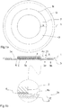
- FIG. 1a is shown in this embodiment, at least on an inner circumference 1i circular film frame 1, at its bottom in accordance with the in FIG. 1b shown sectional view of a film 3 with its adhesive layer 3s is glued concentrically to the film frame 1.
- a product substrate-carrier substrate composite adhered to the adhesive layer 3s of the film 3 concentrically with the film frame 1.
- the product substrate-carrier substrate composite consists of a product substrate 4 adhering to the film 3, a carrier substrate 2, and a bonding layer 6 connecting the product substrate 4 and the carrier substrate 2.
- the diameters of the product substrate 4 and the carrier substrate 2 are substantially identical, while the thickness of the product substrate 4 Product substrate 4 is less than the thickness of the carrier substrate. 2
- the film 3 consists of a ring-shaped fastening section 3b in the present case, in which the film 3 is fixed to the film frame 1. Furthermore, the film 3 consists of a contacting surface portion 3k in which the product substrate 4 is fixable to the adhesive layer 3s of the film 3. Between the attachment portion 3b and the contacting surface portion 3k is a detachment portion 3a arranged, in particular concentric with the attachment portion 3b and the contacting surface portion 3k, which does not have to have an adhesive function, but which has a decisive function according to the invention.
- the detaching portion 3a thus extends from a periphery 4u of the product substrate 4 to the inner periphery 1i of the film frame 1, herein referred to as a radial distance A.
- the ratio between a thickness D of the film frame 1 and the distance A is advantageously at least 1: 2 to 1:50, in particular 1: 5 to 1:25.
- FIG. 1b As shown starting position, the film 3 contacting side of the product substrate 4 and the film 3 contacting side of the film frame 1 are arranged in alignment and in a plane E.
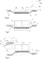
- the in the FIGS. 1a and 1b parts shown are assembled on a known film frame mounter.
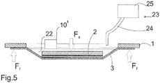
- the film 3 and the inner periphery 1i of the film frame 1 form a trough-shaped solvent container 20 in which the product substrate-carrier substrate composite can be arranged as described above.
- solvent shown 22 by introduction means 23 in the solvent container 20 can be introduced.
- the introduction means 23 in the present case consist of a line 24 and a solvent reservoir 25 which can be controlled by a central unit in order to introduce solvent 22 into the solvent container 20.
- the solvent container 20 is variable in volume by the elastic film 3, which is elastic at least in the detachment section 3a, in that a force F s acts on the carrier substrate 2 downward and a force F f acts on the film frame 1.
- the introduction of force is also controlled by a central unit.
- Enlarging the storage tank volume prevents solvent 22 from passing over the edge of the film frame 1, and at the same time, allows rapid distribution or introduction of the solvent 22.
- the force F s is according to FIG. 3 transmitted via a carrier substrate receptacle 7 for receiving the carrier substrate 2, wherein the fixing of the carrier substrate 2 takes place on the carrier substrate receptacle 7 by incorporated into the surface of the carrier substrate receptacle 7 vacuum webs 8 and connected thereto, not dargschreib vacuum device.
- an acoustic wave generator 10 in particular for generating ultrasonic waves, can be arranged, by which ultrasonic waves can be transmitted to the product substrate 4, but in particular to the bonding layer 6 and the solvent 22, as a result of the process of L Kunststoffs is greatly accelerated, in particular by a factor of 2, preferably by a factor of 5, more preferably by a factor of 10 to 50.
- the sound wave generator 10 is in contact at least with the surface of the fluid solvent 22, but is preferably at least partially immersed therein.
- the sound waves can be transmitted directly to the solvent 22 and from the solvent 22 to the bonding layer 6.
- the force F f acting on the film frame 1 can - as in FIG. 3 shown - evenly distributed as a surface force acting on the film frame 1, so that on the deformation of the film 3 in the detachment section 3a, the change in volume of the solvent container 20 can be effected.
- the force F f1 or a plurality of forces F f1 , F f2 to F fn can / may be introduced at points distributed on the circumference of the film frame 1 or distributed by a film frame recording introduced.
- the receiving device for introducing the force into the film frame 1 a tilting of the film frame 1 must be permitting.
- FIG. 3 illustrated method step of dissolution by the solvent 22 and in FIG. 4 illustrated step of detachment by opposing forces F s , F f1 , F f2 , F fn may be provided a method step by which the solvent 22 is removed from the solvent container 20, in particular by suction.
Landscapes
- Engineering & Computer Science (AREA)
- Computer Hardware Design (AREA)
- Physics & Mathematics (AREA)
- Condensed Matter Physics & Semiconductors (AREA)
- General Physics & Mathematics (AREA)
- Manufacturing & Machinery (AREA)
- Microelectronics & Electronic Packaging (AREA)
- Power Engineering (AREA)
- Mechanical Engineering (AREA)
- Container, Conveyance, Adherence, Positioning, Of Wafer (AREA)
- Laminated Bodies (AREA)
- Application Of Or Painting With Fluid Materials (AREA)
- Mechanical Treatment Of Semiconductor (AREA)
- Adhesives Or Adhesive Processes (AREA)
Description
Die Erfindung betrifft eine Vorrichtung gemäß Anspruch 1 und ein Verfahren gemäß Anspruch 4 zum Ablösen eines Produktsubstrats von einem Trägersubstrat.The invention relates to a device according to
Das Rückdünnen von Produktsubstraten ist in der Halbleiterindustrie häufig erforderlich und kann mechanisch und/oder chemisch erfolgen. Zum Rückdünnen werden die Produktsubstrat in der Regel auf einen Träger vorübergehend fixiert, wobei es für die Fixierung verschiedene Methoden gibt. Als Trägermaterial werden beispielsweise Folien, Glassubstrate oder Siliziumwafer verwendet.The thinning of product substrates is often required in the semiconductor industry and can be mechanical and / or chemical. For re-thinning, the product substrates are usually temporarily fixed to a carrier, with different methods of fixation. The carrier material used is, for example, films, glass substrates or silicon wafers.
Die Druckschrift
In Abhängigkeit von den verwendeten Trägermaterialien und der verwendeten Verbindungsschicht zwischen Träger und Produktsubstrat sind verschiedene Verfahren zur Auflösung oder Zerstörung der Verbindungsschicht bekannt, wie beispielsweise die Verwendung von UV-Licht, Laserstrahlen, Temperatureinwirkung oder Lösungsmittel. Das Ablösen stellt sich zunehmend als einer der kritischsten Prozessschritte dar, da die dünnen Substrate mit Substratdicken von wenigen µm beim Ablösen/Abziehen leicht brechen oder durch die für den Vorgang des Ablösens notwendigen Kräfte Schaden erleiden. Darüber hinaus haben die dünnen Substrate kaum bis keine Formstabilität und rollen sich typischerweise ohne Stützmaterial ein. Während der Handhabung der rückgedünnten Wafer ist mithin eine Fixierung und Unterstützung der Wafer praktisch unumgänglich.Depending on the carrier materials used and the bonding layer used between the carrier and the product substrate, various methods for dissolving or destroying the Bonding known, such as the use of UV light, laser beams, temperature or solvent. The detachment is increasingly considered to be one of the most critical process steps, since the thin substrates with substrate thicknesses of a few microns easily break during peeling / peeling or suffer from the necessary forces for the process of detachment forces. In addition, the thin substrates have little to no dimensional stability and typically curl without support material. Thus, during the handling of the back-thinned wafers, fixing and supporting the wafers is practically unavoidable.
Es ist daher die Aufgabe der vorliegenden Erfindung, eine Vorrichtung und ein Verfahren anzugeben, um ein Produktsubstrat möglichst zerstörungsfrei und einfach von einem Träger zu lösen.It is therefore an object of the present invention to provide an apparatus and a method for releasing a product substrate as non-destructively and easily as possible from a carrier.
Diese Aufgabe wird mit den Merkmalen der Ansprüche 1 und 4 gelöst. Vorteilhafte Weiterbildungen der Erfindung sind in den Unteransprüchen angegeben.This object is achieved with the features of
Den Ausführungsbeispielen liegt der Gedanke zugrunde, eine gattungsgemäße Vorrichtung beziehungsweise ein gattungsgemäßes Verfahren dadurch weiterzubilden, indem Lösungsmittel in einen durch den Filmrahmen und den daran befestigten Film gebildeten Lösungsmittelbehälter eingebracht wird. Durch die Elastizität oder Flexibilität des auf dem Filmrahmen montierten Films ist es gleichzeitig möglich, den Lösungsmittelbehälter volumenveränderlich zu gestalten und die Elastizität oder Flexibilität des Films wird erfindungsgemäß außerdem genutzt, um das Produktsubstrat schonend und vom Rand des Produktsubstrats her abzulösen. Auf diese Weise steht das Produktsubstrat unmittelbar nach dem Abtrennen für weitere Prozessschritte zur Verfügung und ist durch den Film und den Filmrahmen geschützt. Viele Prozessschritte können direkt an dem filmrahmenmontierten Produktsubstrat durchgeführt werden.The exemplary embodiments are based on the idea of developing a generic device or a generic method by introducing solvents into a solvent container formed by the film frame and the film attached thereto becomes. Due to the elasticity or flexibility of the film mounted on the film frame, it is simultaneously possible to make the solvent container volume variable and the elasticity or flexibility of the film is also used according to the invention to gently strip the product substrate and detach it from the edge of the product substrate. In this way, the product substrate is immediately after separation available for further process steps and is protected by the film and the film frame. Many process steps can be performed directly on the film frame mounted product substrate.
Mit Produktsubstrat ist ein Produktsubstrat, beispielsweise ein Halbleiterwafer, gemeint, das üblicherweise auf eine Dicke zwischen 0,5 µm und 250 µm gedünnt ist, wobei die Tendenz zu immer dünneren Produktsubstraten geht. Besonders effektiv arbeitet die vorliegende Erfindung mit Produktsubstraten, die selbst eine ähnliche Flexibilität wie der am Filmrahmen montierte Film aufweisen. Das Produktsubstrat wird bei der erfindungsgemäßen Vorrichtung beziehungsweise dem erfindungsgemäßen Verfahren von dem Trägersubstrat abgeschält, insbesondere konzentrisch vom Umfang des Produktsubstrats ausgehend.By product substrate is meant a product substrate, for example a semiconductor wafer, which is usually thinned to a thickness of between 0.5 μm and 250 μm, with the tendency for ever thinner product substrates. Particularly effectively, the present invention operates with product substrates that themselves have similar flexibility to the film frame mounted film. The product substrate is peeled off the carrier substrate in the device according to the invention or the method according to the invention, in particular starting concentrically from the circumference of the product substrate.
Als Träger wird beispielsweise ein Trägersubstrat mit einer Dicke zwischen 50 µm und 5.000 µm, insbesondere zwischen 500 µm und 1000 µm verwendet.The carrier used is, for example, a carrier substrate having a thickness of between 50 μm and 5,000 μm, in particular between 500 μm and 1000 μm.
Als Verbindungsschicht kommt ein Kleber, beispielsweise ein lösbarer Kleber, insbesondere ein Thermoplast in Frage, der beispielsweise selektiv in einem Randbereich des Träger-Produktsubstrat-Verbundes, insbesondere in einer Randzone von 0,1 bis 20 mm, aufgebracht wird. Alternativ kann der Kleber vollflächig aufgebracht werden, wobei die Klebekraft im Zentrum durch eine haftreduzierende Schicht, beispielsweise ein Fluorpolymer, vorzugsweise Teflon, reduziert sein kann.As a bonding layer, an adhesive, for example a releasable adhesive, in particular a thermoplastic in question, for example, selectively in an edge region of the carrier-product substrate composite, in particular in an edge zone of 0.1 to 20 mm applied. Alternatively, the adhesive can be applied over the entire surface, with the adhesive force in the center being reduced by an adhesion-reducing layer, For example, a fluoropolymer, preferably Teflon, can be reduced.
Als Aufnahmeeinrichtung eignet sich besonders ein Chuck, insbesondere ein Spinner Chuck zur Aufnahme des Trägersubstrats, insbesondere mittels Unterdruck, beispielsweise an Saugbahnen, Bohrungen oder Saugnäpfen. Alternativ ist eine mechanische Aufnahme, beispielsweise durch seitliche Klammern, denkbar. In einer weiteren, alternativen Ausgestaltung erfolgt die Aufnahme elektrostatisch.Particularly suitable as a receiving device is a chuck, in particular a spinner chuck for receiving the carrier substrate, in particular by means of negative pressure, for example on suction paths, holes or suction cups. Alternatively, a mechanical recording, for example by lateral brackets, conceivable. In a further, alternative embodiment, the recording takes place electrostatically.
Die Ablösungsmittel umfassen den auf den Filmrahmen montierten Film und eine den Filmrahmen aufnehmende und kraftbeaufschlagende Filmrahmenaufnahme.The release means comprises the film mounted on the film frame and a film frame receiving and force loading film frame receiver.
In einer vorteilhaften Ausführungsform ist vorgesehen, dass das Lösungsmittel im Wesentlichen erhitzungsfrei arbeitend ausgebildet ist. Das Lösungsmittel wird vorzugsweise bei Umgebungstemperatur eingesetzt. Auf diese Weise ist es möglich, auf jegliche Heizeinrichtung zu verzichten.In an advantageous embodiment, it is provided that the solvent is formed substantially free of heating working. The solvent is preferably used at ambient temperature. In this way it is possible to dispense with any heating device.
Indem das Lösungsmittel zur zumindest partiellen Lösung der durch die Verbindungsschicht bewirkten Verbindung zwischen dem Trägersubstrat und dem Produktsubstrat vorgesehen ist, wird das Ablösen durch die Ablösemittel mit Vorteil deutlich erleichtert.By providing the solvent for the at least partial dissolution of the connection layer between the carrier substrate and the product substrate, peel-off is advantageously facilitated by the release means.
Dadurch, dass das Lösungsmittel, insbesondere ein die Verbindungsschicht selektiv auflösendes, Fluidmittel zur zumindest partiellen Lösung der Verbindungsschicht umfasst, wird bei verschiedene Kleber umfassenden Verbindungsschichten ermöglicht, eine bestimmte Verbindungsschicht gezielt oder in definierten Regionen aufzulösen. Die chemische Auflösung der Verbindungssicht ist für das Produktsubstrat dabei besonders schonend und bei entsprechender Materialwahl kann die Auflösung auch sehr schnell erfolgen, insbesondere wenn nur Randbereiche des Produktsubstrats mit einer Verbindungsschicht versehen sind, so dass das Lösungsmittel von der Seite her schnell wirken kann. Auf diese Weise kann auf Perforierungen im Trägersubstrat und/oder Produktsubstrat verzichtet werden.By virtue of the fact that the solvent, in particular a fluid medium which selectively dissolves the connecting layer, comprises at least partial dissolution of the connecting layer, connection layers comprising different adhesives make it possible to dissolve a specific connecting layer selectively or in defined regions. The chemical dissolution of the bonding view is particularly gentle for the product substrate and with appropriate choice of material, the dissolution can also be very fast, especially if only edge regions of the product substrate are provided with a bonding layer, so that the solvent can act quickly from the side. In this way it is possible to dispense with perforations in the carrier substrate and / or product substrate.
Soweit der Lösungsmittelbehälter derart ausgebildet ist, dass das Lösungsmittel zumindest am Beginn des Lösens der Verbindungsschicht, insbesondere ausschließlich, im Bereich eines Umfangs des Produktsubstrats wirkt, kann auf eine Einwirkung des Produktsubstrats und/oder Trägersubstrats von der Oberseite und/oder der Unterseite, insbesondere einem innerhalb des Seitenrandes liegenden Innenbereich des Produktsubstrats, verzichtet werden.As far as the solvent container is formed such that the solvent acts at least at the beginning of the release of the bonding layer, in particular exclusively, in the region of a circumference of the product substrate, may be on an action of the product substrate and / or carrier substrate from the top and / or bottom, in particular one Within the side edge lying inside area of the product substrate can be dispensed with.
Erfindungsgemäß ist vorgesehen, dass die Ablösungsmittel eine auf das Trägersubstrat wirkende Kraft Fs und eine entgegen der Kraft Fs gerichtete, auf den Filmrahmen wirkenden Kraft Ff bewirkend ausgebildet sind. Hierdurch wird auf einfache und durch den Film besonders schonende Art und Weise das Ablösen bewerkstelligt. Die Kraft Ff wirkt am Umfang des Filmrahmens, an mindestens zwei, über den Umfang verteilten Stellen des Filmrahmens, wobei die Kräfte Ff1 und Ff2 erfindungsgemäß unterschiedlich gesteuert werden können, um das Produktsubstrat von der Seite her mit der größeren Kraft Ff abzulösen.According to the invention, it is provided that the release means have a force F s acting on the carrier substrate and a force F f directed against the force F s and acting on the film frame. As a result, in a simple and particularly gentle way through the film, the detachment accomplished. The force F f acts on the circumference of the film frame, at least two circumferentially distributed locations of the film frame, wherein the forces F f1 and F f2 can be controlled differently according to the invention to detach the product substrate from the side with the larger force F f ,
Dabei ist es von besonderem Vorteil, wenn der Film, insbesondere durch die Kraft Fs und die Kraft Ff, in einem zwischen dem Kontaktierungsflächenabschnitt und dem Befestigungsabschnitt liegenden Ablöseabschnitt spannbar ist. Hierdurch wird das Ablösen schonend am Umfang des Produktsubstrats bewirkt. Das Lösen durch das Lösungsmittel und das Ablösen durch die Kräfte Fs und Ff unterstützt sich dabei gegenseitig.It is particularly advantageous if the film, in particular by the force Fs and the force Ff, in a between the Contacting surface portion and the attachment portion lying release portion is tensioned. As a result, the detachment is effected gently on the circumference of the product substrate. The release by the solvent and the detachment by the forces F s and F f supports each other.
Gemäß einer vorteilhaften Ausführungsform ist vorgesehen, dass ein auf das Lösungsmittel und/oder die Verbindungsschicht einwirkender, insbesondere am Film anliegender und/oder in das Lösungsmittel im Lösungsmittelbehälter einbringbarer, Schwingungserzeuger vorgesehen ist. Einbringbar umfasst sowohl einen Oberflächenkontakt als auch ein zumindest teilweises Eintauchen. Dieser unterstützt das Lösen durch das Lösungsmittel und beschleunigt den Lösungsvorgang mindestens um den Faktor 2, bei optimierter Ausgestaltung um den Faktor 5, noch bevorzugter um den Faktor 10 bis 50. Vorzugsweise wirkt der Schwingungserzeuger durch Ultraschallwellen, insbesondere im Bereich des Kontaktierungsflächenabschnitts.According to an advantageous embodiment, it is provided that a vibration generator acting on the solvent and / or the bonding layer, in particular on the film and / or insertable into the solvent in the solvent container, is provided. Applicable includes both surface contact and at least partial immersion. This supports the dissolution by the solvent and accelerates the dissolution process by at least a factor of 2, with an optimized embodiment by a factor of 5, more preferably by a factor of 10 to 50. Preferably, the vibration generator by ultrasonic waves, in particular in the region of Kontaktierungsflächenabschnitts.
In einer weiteren vorteilhaften Ausführungsform ist der Lösungsmittelbehälter wannenförmig ausgebildet, wodurch mit einem minimalen Lösungsmittelverbrauch die Ablösung des Produktsubstrats erreicht werden kann.In a further advantageous embodiment, the solvent container is trough-shaped, whereby the detachment of the product substrate can be achieved with a minimum solvent consumption.
Weitere Vorteile, Merkmale und Einzelheiten der Erfindung ergeben sich aus der nachfolgenden Beschreibung bevorzugter Ausführungsbeispiele sowie anhand der Zeichnungen; diese zeigen in:
- Fig. 1a:
- Eine schematische Aufsicht auf einen aus Produktsubstrat, Trägersubstrat und Verbindungsschicht bestehenden Substratverbund auf einem Filmrahmen,
- Fig. 1b:
- eine schematische Seitenansicht zu
Figur 1a mit einer Detailansicht, - Figur 2:
- eine schematische Darstellung gemäß
Figur 2 Figur 3- eine schematische Darstellung eines Verfahrensausschnitts des Lösens der Verbindungsschicht,
- Figur 4:
- eine schematische Darstellung eines erfindungsgemäßen Verfahrensschritts des Ablösens des Produktsubstrats vom Trägersubstrat.
- Figur 5:
- eine schematische Darstellung eines alternativen erfindungsgemäßen Verfahrensschritts des Ablösens des Produktsubstrats vom Trägersubstrat.
- Fig. 1a:
- A schematic plan view of a substrate composite consisting of product substrate, carrier substrate and connecting layer on a film frame,
- Fig. 1b:
- a schematic side view to
FIG. 1a with a detailed view, - FIG. 2:
- a schematic representation according to
FIG. 2 when introducing the solvent, - FIG. 3
- a schematic representation of a process section of the release of the bonding layer,
- FIG. 4:
- a schematic representation of a method step according to the invention of the detachment of the product substrate from the carrier substrate.
- FIG. 5:
- a schematic representation of an alternative method step according to the invention of the detachment of the product substrate from the carrier substrate.
In den Figuren sind gleiche Bauteile und Bauteile mit der gleichen Funktion mit den gleichen Bezugszeichen gekennzeichnet.In the figures, the same components and components with the same function with the same reference numerals.
In
Der Film 3 besteht aus einem im vorliegenden Fall kreisringförmigen Befestigungsabschnitt 3b, in welchem der Film 3 mit dem Filmrahmen 1 fixiert ist. Weiterhin besteht der Film 3 aus einem Kontaktierungsflächenabschnitt 3k, in welchem das Produktsubstrat 4 an der Klebeschicht 3s des Films 3 fixierbar ist. Zwischen dem Befestigungsabschnitt 3b und dem Kontaktierungsflächenabschnitt 3k liegt ein, insbesondere konzentrisch zu dem Befestigungsabschnitt 3b und dem Kontaktierungsflächenabschnitt 3k angeordneter Ablöseabschnitt 3a, der keine Klebefunktion aufweisen muss, dem aber eine erfindungsgemäß entscheidende Funktion zukommt. Der Ablöseabschnitt 3a erstreckt sich damit von einem Umfang 4u des Produktsubstrats 4 bis zu dem Innenumfang 1i des Filmrahmens 1, vorliegend als Radialabstand A bezeichnet. Das Verhältnis zwischen einer Dicke D des Filmrahmens 1 und des Abstands A beträgt im Vorteil mindestens 1:2 bis 1:50, insbesondere 1:5 bis 1:25.The
In der in
Der Film 3 und der Innenumfang 1i des Filmrahmens 1 bilden einen wannenförmigen Lösungsmittelbehälter 20, in welchem wie vorbeschrieben der Produktsubstrat-Trägersubstrat-Verbund anordenbar ist.The
Gemäß dem in
Wie in
Durch die Vergrößerung des Vorratsmittelbehältervolumens wird verhindert, dass Lösungsmittel 22 über den Rand des Filmrahmens 1 läuft und gleichzeitig wird eine schnelle Verteilung oder Einbringung des Lösungsmittels 22 ermöglicht.Enlarging the storage tank volume prevents solvent 22 from passing over the edge of the
Die Kraft Fs wird gemäß
Auf der gegenüberliegenden Seite des Films 3 zum Produktsubstrat 4 ist ein Schallwellenerzeuger 10, insbesondere zur Erzeugung von Ultraschallwellen, anordenbar, durch welchen Ultraschallwellen auf das Produktsubstrat 4, insbesondere jedoch auf die Verbindungsschicht 6 und das Lösungsmittel 22 übertragen werden können, da hierdurch der Vorgang des Lösens stark beschleunigt wird, insbesondere um eine Faktor 2, vorzugsweise um eine Faktor 5, noch bevorzugter um einen Faktor 10 bis 50.On the opposite side of the
Gemäß einer alternativen, in
Die auf den Filmrahmen 1 wirkende Kraft Ff kann - wie in
Umgekehrt erfolgt gemäß
Die Kraft Ff1 beziehungsweise mehrere Kräfte Ff1, Ff2 bis Ffn kann/können punktuell verteilt am Umfang des Filmrahmens 1 eingeleitet werden oder durch eine Filmrahmenaufnahme verteilt eingebracht werden.The force F f1 or a plurality of forces F f1 , F f2 to F fn can / may be introduced at points distributed on the circumference of the
Soweit die Kräfte Ff1, Ff2 und/oder Ffn unterschiedlich ausgebildet sind, muss die Aufnahmeeinrichtung zur Einleitung der Kraft in den Filmrahmen 1 ein Kippen des Filmrahmens 1 zulassend ausgebildet sein.As far as the forces F f1 , F f2 and / or F fn are formed differently, the receiving device for introducing the force into the
Zwischen dem in
- 11
- Filmrahmenfilm frame
- 22
- Trägersubstratcarrier substrate
- 33
- FilmMovie
- 3a3a
- Ablöseabschnitttransfer section
- 3b3b
- Befestigungsabschnittattachment section
- 3k3k
- KontaktierungsflächenabschnittKontaktierungsflächenabschnitt
- 3s3s
- Klebeschichtadhesive layer
- 44
- Produktsubstratproduct substrate
- 4u4u
- Umfangscope
- 66
- Verbindungsschichtlink layer
- 77
- TrägersubstrataufnahmeCarrier substrate uptake
- 88th
- Vakuumbahnenvacuum tracks
- 10, 10'10, 10 '
- SchallwellenerzeugerSound wave generator
- 2020
- LösungsmittelbehälterSolvent containers
- 2222
- Lösungsmittelsolvent
- 2323
- Einbringmittelinsertion means
- 2424
- Leitungmanagement
- 2525
- LösungsmittelvorratSolvent reservoir
- Ff, Ff1, Ff2 ... Ffn F f , F f1, F f2 ... F fn
- Kraftforce
- Fsfs
- Kraftforce
Claims (6)
- Device for stripping a product substrate (4) off a carrier substrate (2) connected to the product substrate (4) by a bonding layer (6), wherein the product substrate (4) is received on with a flexible film (3) which has an adhesive layer (3s) for holding the product substrate (4) in a contacting surface section (3k) of the film (3), and wherein the film (3) being connected to a film frame (1) in an attachment section (3b) of the film (3) which surrounds the contacting surface section (3k), with the following features:- stripping means for stripping the product substrate (4) off the carrier substrate (2) by means of a force Fs,characterized in that at least two differently controllable forces FF1 and FF2 acting on the periphery of film frame (1) and distributed over the periphery are applicable in opposed directions.
- Device as claimed in claim 1, wherein the film (3) can be clamped, especially by the force Fs and force Ff, in a stripping section (3a) which lies between the contacting surface section (3k) and the attachment section (3b).
- Device as claimed in one of the preceding claims, wherein the stripping means are made to act concentrically from the periphery (4u) of the product substrate (4) to the center (4z) of the product substrate (4).
- Method for stripping a product substrate (4) off a carrier substrate (2) connected with the product substrate (4) by means of a bonding layer (6), wherein the product substrate (4) is received on with a flexible film (3) which has an adhesive layer (3s) for holding the product substrate (4) in a contacting surface section (3k) of the film (3), and wherein the film (3) being connected to a film frame (1) in an attachment section (3b) of the film (3) which surrounds the contacting surface section (3k), with the following steps:- detaching the product substrate (4) from the carrier substrate (2) by means of a force Fs, characterized in that at least two differently controllable forces FF1 and FF2 acting on the periphery of film frame (1) and distributed over the periphery are applied in opposed directions.
- Method as claimed in Claim 4, wherein the stripping means is effected concentrically from the periphery (4u) of the product substrate (4) to the center (4z) of the product substrate (4).
- Method as claimed in Claim 4 or 5, wherein the product substrate (4) is bonded to the carrier substrate (2) by means of a bonding layer containing different adhesives.
Priority Applications (1)
| Application Number | Priority Date | Filing Date | Title |
|---|---|---|---|
| EP12179539.7A EP2523209B1 (en) | 2010-04-23 | 2010-04-23 | Device and method for releasing a product substrate from a holder substrate |
Applications Claiming Priority (2)
| Application Number | Priority Date | Filing Date | Title |
|---|---|---|---|
| EP10004313A EP2381464B1 (en) | 2010-04-23 | 2010-04-23 | Device and method for releasing a product substrate from a holder substrate |
| EP12179539.7A EP2523209B1 (en) | 2010-04-23 | 2010-04-23 | Device and method for releasing a product substrate from a holder substrate |
Related Parent Applications (2)
| Application Number | Title | Priority Date | Filing Date |
|---|---|---|---|
| EP10004313.2 Division | 2010-04-23 | ||
| EP10004313A Division EP2381464B1 (en) | 2010-04-23 | 2010-04-23 | Device and method for releasing a product substrate from a holder substrate |
Publications (2)
| Publication Number | Publication Date |
|---|---|
| EP2523209A1 EP2523209A1 (en) | 2012-11-14 |
| EP2523209B1 true EP2523209B1 (en) | 2017-03-08 |
Family
ID=42356878
Family Applications (3)
| Application Number | Title | Priority Date | Filing Date |
|---|---|---|---|
| EP10004313A Active EP2381464B1 (en) | 2010-04-23 | 2010-04-23 | Device and method for releasing a product substrate from a holder substrate |
| EP12179539.7A Active EP2523209B1 (en) | 2010-04-23 | 2010-04-23 | Device and method for releasing a product substrate from a holder substrate |
| EP12179537.1A Active EP2523208B1 (en) | 2010-04-23 | 2010-04-23 | Device and method for releasing a product substrate from a holder substrate |
Family Applications Before (1)
| Application Number | Title | Priority Date | Filing Date |
|---|---|---|---|
| EP10004313A Active EP2381464B1 (en) | 2010-04-23 | 2010-04-23 | Device and method for releasing a product substrate from a holder substrate |
Family Applications After (1)
| Application Number | Title | Priority Date | Filing Date |
|---|---|---|---|
| EP12179537.1A Active EP2523208B1 (en) | 2010-04-23 | 2010-04-23 | Device and method for releasing a product substrate from a holder substrate |
Country Status (8)
| Country | Link |
|---|---|
| US (3) | US9272501B2 (en) |
| EP (3) | EP2381464B1 (en) |
| JP (4) | JP5623623B2 (en) |
| KR (3) | KR101476516B1 (en) |
| CN (2) | CN103219265B (en) |
| SG (1) | SG183305A1 (en) |
| TW (3) | TWI421929B (en) |
| WO (1) | WO2011131283A1 (en) |
Families Citing this family (19)
| Publication number | Priority date | Publication date | Assignee | Title |
|---|---|---|---|---|
| EP2381464B1 (en) * | 2010-04-23 | 2012-09-05 | EV Group GmbH | Device and method for releasing a product substrate from a holder substrate |
| JP5558191B2 (en) * | 2010-04-27 | 2014-07-23 | 東京応化工業株式会社 | Peeling apparatus and peeling method |
| KR102064405B1 (en) | 2014-02-04 | 2020-01-10 | 삼성디스플레이 주식회사 | Substrate peeling apparatus and substrate peeling method using the same |
| KR102165162B1 (en) | 2014-03-12 | 2020-10-14 | 삼성디스플레이 주식회사 | Substrate peeling apparatus and method of manufacturing device using the same |
| JP6216727B2 (en) * | 2014-05-08 | 2017-10-18 | 東京応化工業株式会社 | Support separation method |
| JP6268483B2 (en) * | 2014-06-03 | 2018-01-31 | 旭硝子株式会社 | Laminate peeling apparatus, peeling method, and electronic device manufacturing method |
| SG11201603148VA (en) * | 2014-12-18 | 2016-07-28 | Ev Group E Thallner Gmbh | Method for bonding substrates |
| JP2016146429A (en) * | 2015-02-09 | 2016-08-12 | トヨタ自動車株式会社 | Semiconductor device manufacturing method |
| US10343417B2 (en) * | 2015-07-15 | 2019-07-09 | Hewlett-Packard Development Company, L.P. | Diagnostic plot for printing system |
| CN106053505A (en) * | 2016-05-17 | 2016-10-26 | 深圳市宁深检验检测技术有限公司 | Method for rapidly measuring gold content and gold quality of gold sheet with film coated surface |
| JP7000129B2 (en) * | 2017-11-15 | 2022-01-19 | 芝浦メカトロニクス株式会社 | Film forming equipment |
| JP6935306B2 (en) * | 2017-11-16 | 2021-09-15 | 芝浦メカトロニクス株式会社 | Film deposition equipment |
| HUE054704T2 (en) * | 2018-12-06 | 2021-09-28 | Heraeus Deutschland Gmbh & Co Kg | Packaging unit for substrates |
| JP7146354B2 (en) * | 2019-01-22 | 2022-10-04 | 株式会社ディスコ | Carrier plate removal method |
| KR102191204B1 (en) * | 2019-07-31 | 2020-12-15 | 삼영공업 주식회사 | Apparatus for separating connected plates and method for separating the same |
| JP7262903B2 (en) * | 2019-08-26 | 2023-04-24 | 株式会社ディスコ | Carrier plate removal method |
| JP7262904B2 (en) * | 2019-08-26 | 2023-04-24 | 株式会社ディスコ | Carrier plate removal method |
| KR102298227B1 (en) * | 2019-08-30 | 2021-09-06 | 주식회사 엘트린 | The debonding apparatus for the bonded substrates |
| JP2022020952A (en) * | 2020-07-21 | 2022-02-02 | 株式会社ディスコ | Carrier plate removal method |
Citations (1)
| Publication number | Priority date | Publication date | Assignee | Title |
|---|---|---|---|---|
| US20040166653A1 (en) * | 2002-12-16 | 2004-08-26 | Sebastien Kerdiles | Tools and methods for disuniting semiconductor wafers |
Family Cites Families (59)
| Publication number | Priority date | Publication date | Assignee | Title |
|---|---|---|---|---|
| US3988196A (en) | 1967-10-09 | 1976-10-26 | Western Electric Company, Inc. | Apparatus for transferring an oriented array of articles |
| US4826553A (en) * | 1987-06-18 | 1989-05-02 | The United States Of America As Represented By The Secretary Of The Air Force | Method for replicating an optical element |
| US5273615A (en) | 1992-04-06 | 1993-12-28 | Motorola, Inc. | Apparatus and method for handling fragile semiconductor wafers |
| JPH06275717A (en) * | 1993-01-22 | 1994-09-30 | Mitsubishi Electric Corp | Wafer peeling method |
| JPH06268051A (en) | 1993-03-10 | 1994-09-22 | Mitsubishi Electric Corp | Wafer stripper |
| JP4220580B2 (en) | 1995-02-10 | 2009-02-04 | 三菱電機株式会社 | Semiconductor device manufacturing equipment |
| JP3407835B2 (en) | 1995-03-09 | 2003-05-19 | 東京応化工業株式会社 | Method and apparatus for removing edge coating on substrate |
| US6342434B1 (en) * | 1995-12-04 | 2002-01-29 | Hitachi, Ltd. | Methods of processing semiconductor wafer, and producing IC card, and carrier |
| JP2004119975A (en) * | 1995-12-04 | 2004-04-15 | Renesas Technology Corp | Method of manufacturing ic card |
| DE19734635A1 (en) | 1997-08-11 | 1999-02-18 | Gen Semiconductor Ireland Macr | Component separation method for removal from foil |
| US6090687A (en) | 1998-07-29 | 2000-07-18 | Agilent Technolgies, Inc. | System and method for bonding and sealing microfabricated wafers to form a single structure having a vacuum chamber therein |
| JP2001196404A (en) | 2000-01-11 | 2001-07-19 | Fujitsu Ltd | Semiconductor device and method of manufacturing the same |
| JP3768069B2 (en) | 2000-05-16 | 2006-04-19 | 信越半導体株式会社 | Thinning method of semiconductor wafer |
| DE10048881A1 (en) | 2000-09-29 | 2002-03-07 | Infineon Technologies Ag | Device for planar joining of two wafers e.g. for thin grinding and separation of product-wafer, has product wafer arranged surface-congruently over carrier wafer |
| JP2002237515A (en) | 2001-02-07 | 2002-08-23 | Mitsubishi Gas Chem Co Inc | Peeling device and peeling method for making semiconductor substrate into thin sheet |
| US6713880B2 (en) | 2001-02-07 | 2004-03-30 | Matsushita Electric Industrial Co., Ltd. | Semiconductor device and method for producing the same, and method for mounting semiconductor device |
| DE10108369A1 (en) | 2001-02-21 | 2002-08-29 | B L E Lab Equipment Gmbh | Method and device for detaching a semiconductor wafer from a carrier |
| AT502233B1 (en) | 2001-06-07 | 2007-04-15 | Thallner Erich | Carrier detachment device aligns inner, near-edge surface of frame with semiconductor disk and bonds them to foil, before detaching disk from carrier |
| JPWO2003081584A1 (en) | 2002-03-27 | 2005-07-28 | 松下電器産業株式会社 | Method for producing multilayer optical information recording medium |
| JP4271409B2 (en) * | 2002-05-22 | 2009-06-03 | リンテック株式会社 | Processing method for brittle materials |
| TWI258316B (en) | 2002-10-25 | 2006-07-11 | Ritdisplay Corp | FPD encapsulation apparatus and method for encapsulating ehereof |
| JP2004193237A (en) | 2002-12-10 | 2004-07-08 | Disco Abrasive Syst Ltd | Wafer retaining member equipped with pressure sensitive adhesive sheet and peeling method of pressure sensitive adhesive sheet |
| JP4364535B2 (en) | 2003-03-27 | 2009-11-18 | シャープ株式会社 | Manufacturing method of semiconductor device |
| JP4474854B2 (en) | 2003-07-02 | 2010-06-09 | Jsr株式会社 | Radiation-sensitive adhesive composition and wafer processing method using the same |
| DE10340409B4 (en) | 2003-09-02 | 2007-05-24 | Fraunhofer-Gesellschaft zur Förderung der angewandten Forschung e.V. | Carrier wafer and method for processing a semiconductor wafer using a carrier wafer |
| JP3912350B2 (en) * | 2003-09-22 | 2007-05-09 | 住友電気工業株式会社 | Manufacturing method of semiconductor device |
| JP4447280B2 (en) | 2003-10-16 | 2010-04-07 | リンテック株式会社 | Surface protection sheet and semiconductor wafer grinding method |
| JP2005191535A (en) * | 2003-12-01 | 2005-07-14 | Tokyo Ohka Kogyo Co Ltd | Sticking device and sticking method |
| JP2006135272A (en) | 2003-12-01 | 2006-05-25 | Tokyo Ohka Kogyo Co Ltd | Substrate support plate and peeling method of support plate |
| DE102004018250A1 (en) | 2004-04-15 | 2005-11-03 | Infineon Technologies Ag | Wafer stabilization device and method for its production |
| JP2005353859A (en) | 2004-06-11 | 2005-12-22 | Taiyo Yuden Co Ltd | Exfoliation method of semiconductor wafer |
| US7829152B2 (en) | 2006-10-05 | 2010-11-09 | Lam Research Corporation | Electroless plating method and apparatus |
| JP2006032506A (en) | 2004-07-14 | 2006-02-02 | Taiyo Yuden Co Ltd | Method and device for peeling semiconductor wafer |
| JP2006059861A (en) * | 2004-08-17 | 2006-03-02 | Lintec Corp | Transferring and bonding device of brittle member |
| JP4679890B2 (en) | 2004-11-29 | 2011-05-11 | 東京応化工業株式会社 | Support plate pasting device |
| US9040420B2 (en) * | 2005-03-01 | 2015-05-26 | Semiconductor Energy Laboratory Co., Ltd. | Manufacturing method of semiconductor device including peeling layers from substrates by etching |
| JP4748518B2 (en) | 2005-07-20 | 2011-08-17 | 古河電気工業株式会社 | Dicing die bond tape and dicing tape |
| JP4848153B2 (en) | 2005-08-10 | 2011-12-28 | ルネサスエレクトロニクス株式会社 | Manufacturing method of semiconductor device |
| JP4721828B2 (en) * | 2005-08-31 | 2011-07-13 | 東京応化工業株式会社 | Support plate peeling method |
| TW200730414A (en) * | 2005-11-18 | 2007-08-16 | Advanced Tech Materials | Material storage and dispensing containers and systems comprising same |
| JP4668052B2 (en) | 2005-12-06 | 2011-04-13 | 東京応化工業株式会社 | Peeling device |
| DE102006000687B4 (en) | 2006-01-03 | 2010-09-09 | Thallner, Erich, Dipl.-Ing. | Combination of a carrier and a wafer, device for separating the combination and methods for handling a carrier and a wafer |
| JP2008021929A (en) * | 2006-07-14 | 2008-01-31 | Tokyo Ohka Kogyo Co Ltd | Support plate, carrying device, and peeling device and peeling method |
| JP5027460B2 (en) * | 2006-07-28 | 2012-09-19 | 東京応化工業株式会社 | Wafer bonding method, thinning method, and peeling method |
| JP4847255B2 (en) * | 2006-08-30 | 2011-12-28 | 株式会社テオス | Processing method of semiconductor wafer |
| JP4402144B2 (en) | 2006-09-29 | 2010-01-20 | 株式会社半導体エネルギー研究所 | Method for manufacturing semiconductor device |
| JP5238927B2 (en) * | 2007-03-14 | 2013-07-17 | セミコンダクター・コンポーネンツ・インダストリーズ・リミテッド・ライアビリティ・カンパニー | Manufacturing method of semiconductor device |
| JP4958287B2 (en) | 2007-05-30 | 2012-06-20 | 東京応化工業株式会社 | Peeling method in peeling device |
| JP5090789B2 (en) | 2007-05-30 | 2012-12-05 | 東京応化工業株式会社 | Bonding apparatus, method for preventing dissolution of adhesive, and bonding method |
| US20090017323A1 (en) * | 2007-07-13 | 2009-01-15 | 3M Innovative Properties Company | Layered body and method for manufacturing thin substrate using the layered body |
| JP5074940B2 (en) * | 2008-01-30 | 2012-11-14 | 東京応化工業株式会社 | Substrate processing method |
| JP2009182256A (en) | 2008-01-31 | 2009-08-13 | Tokyo Ohka Kogyo Co Ltd | Processing device for substrate and processing method for substrate |
| JP4965485B2 (en) | 2008-02-29 | 2012-07-04 | 東京応化工業株式会社 | Treatment liquid permeation unit and treatment apparatus |
| JP2010027720A (en) | 2008-07-16 | 2010-02-04 | Shin Etsu Polymer Co Ltd | Ring frame |
| WO2010023935A1 (en) * | 2008-08-29 | 2010-03-04 | 株式会社ニコン | Substrate aligning apparatus, substrate aligning method and method for manufacturing multilayer semiconductor |
| TWM355799U (en) * | 2008-09-16 | 2009-05-01 | Ye Siang Entpr Co Ltd | Disassembling and assembling jig |
| EP2660851B1 (en) | 2009-03-18 | 2020-10-14 | EV Group GmbH | Device and method for releasing a wafer from a holder |
| EP2381464B1 (en) * | 2010-04-23 | 2012-09-05 | EV Group GmbH | Device and method for releasing a product substrate from a holder substrate |
| CN104247068B (en) * | 2012-04-23 | 2017-12-05 | 南洋理工大学 | Apparatus and method for separating sandwich construction |
-
2010
- 2010-04-23 EP EP10004313A patent/EP2381464B1/en active Active
- 2010-04-23 EP EP12179539.7A patent/EP2523209B1/en active Active
- 2010-04-23 EP EP12179537.1A patent/EP2523208B1/en active Active
-
2011
- 2011-03-29 CN CN201310126332.XA patent/CN103219265B/en active Active
- 2011-03-29 WO PCT/EP2011/001556 patent/WO2011131283A1/en active Application Filing
- 2011-03-29 KR KR1020127022017A patent/KR101476516B1/en active IP Right Grant
- 2011-03-29 KR KR1020127032469A patent/KR101742347B1/en active IP Right Grant
- 2011-03-29 JP JP2013504150A patent/JP5623623B2/en active Active
- 2011-03-29 KR KR1020127032468A patent/KR101454985B1/en active IP Right Grant
- 2011-03-29 SG SG2012060018A patent/SG183305A1/en unknown
- 2011-03-29 US US13/641,479 patent/US9272501B2/en active Active
- 2011-03-29 CN CN201180011757.5A patent/CN103620732B/en active Active
- 2011-04-22 TW TW100114153A patent/TWI421929B/en active
- 2011-04-22 TW TW101145179A patent/TWI447793B/en active
- 2011-04-22 TW TW101145174A patent/TWI520198B/en active
-
2013
- 2013-05-10 JP JP2013099954A patent/JP5714053B2/en active Active
- 2013-06-18 US US13/920,458 patent/US9381729B2/en active Active
-
2014
- 2014-07-28 JP JP2014152881A patent/JP5997732B2/en active Active
-
2015
- 2015-04-13 JP JP2015081502A patent/JP6099688B2/en active Active
- 2015-05-19 US US14/715,691 patent/US9457552B2/en active Active
Patent Citations (1)
| Publication number | Priority date | Publication date | Assignee | Title |
|---|---|---|---|---|
| US20040166653A1 (en) * | 2002-12-16 | 2004-08-26 | Sebastien Kerdiles | Tools and methods for disuniting semiconductor wafers |
Also Published As
Similar Documents
| Publication | Publication Date | Title |
|---|---|---|
| EP2523209B1 (en) | Device and method for releasing a product substrate from a holder substrate | |
| EP2290679B1 (en) | Device and method for releasing a product substrate (e.g., a semiconductor wafer) from a support substrate by deformation of a flexible film mounted on a frame | |
| EP2230683B1 (en) | Device and method for releasing a wafer from a holder | |
| EP2382656B1 (en) | Method for separating a layer system comprising a wafer | |
| DE10260233B4 (en) | Method of attaching a workpiece to a solid on a workpiece carrier and workpiece carrier | |
| DE112013000980B4 (en) | Method for temporarily connecting a product substrate to a carrier substrate and a corresponding composite | |
| DE112009000140T5 (en) | A method of reversibly attaching a device wafer to a carrier substrate | |
| DE102010027703A1 (en) | Method and apparatus for removing a reversibly mounted device wafer from a carrier substrate | |
| DE2504944A1 (en) | SYSTEM FOR SEPARATING A SEMICONDUCTOR PLATE INTO INDIVIDUAL PELLETS | |
| WO2012097830A1 (en) | Method for separating a product substrate from a carrier substrate | |
| DE112016005452B4 (en) | Environmental protection barrier for a chip | |
| EP2553719B1 (en) | Method for producing a wafer provided with chips using two separately detachable carrier wafers with ring-shaped adhesive layers of different ring widths | |
| DE10256247A1 (en) | Process for treating wafers comprises covering the front side of the wafer having components with a layer system consisting of a separating layer and a protective layer before the rear side of the wafer is coated | |
| WO2004032593A2 (en) | Extremely thin substrate support | |
| DE4223215C2 (en) | Process for processing silicon wafers | |
| DE102004004476B3 (en) | Resin cover application to a system wafer, comprises applying a cover to a carrier via a connection layer, and then mechanically removing the carrier and connection layer | |
| DE102019202564A1 (en) | Stripping method for detaching a substrate from a carrier plate | |
| DE102006048800B4 (en) | Hard carrier multilayer system for supporting thin wafers in semiconductor fabrication | |
| DE102006004834B4 (en) | Process for treating wafers during thinning | |
| AT517638B1 (en) | Pick-up device for handling structured substrates | |
| DE102020210751A1 (en) | METHOD OF REMOVING A CARRIER PLATE | |
| DE10262317B4 (en) | Method for separating a workpiece from a workpiece carrier |
Legal Events
| Date | Code | Title | Description |
|---|---|---|---|
| PUAI | Public reference made under article 153(3) epc to a published international application that has entered the european phase |
Free format text: ORIGINAL CODE: 0009012 |
|
| AC | Divisional application: reference to earlier application |
Ref document number: 2381464 Country of ref document: EP Kind code of ref document: P |
|
| AK | Designated contracting states |
Kind code of ref document: A1 Designated state(s): AT BE BG CH CY CZ DE DK EE ES FI FR GB GR HR HU IE IS IT LI LT LU LV MC MK MT NL NO PL PT RO SE SI SK SM TR |
|
| 17P | Request for examination filed |
Effective date: 20130307 |
|
| 17Q | First examination report despatched |
Effective date: 20141212 |
|
| REG | Reference to a national code |
Ref country code: DE Ref legal event code: R079 Ref document number: 502010013291 Country of ref document: DE Free format text: PREVIOUS MAIN CLASS: H01L0021000000 Ipc: H01L0021670000 |
|
| GRAP | Despatch of communication of intention to grant a patent |
Free format text: ORIGINAL CODE: EPIDOSNIGR1 |
|
| RIC1 | Information provided on ipc code assigned before grant |
Ipc: B32B 43/00 20060101ALN20160912BHEP Ipc: H01L 21/673 20060101ALI20160912BHEP Ipc: H01L 21/00 20060101ALI20160912BHEP Ipc: B32B 37/00 20060101ALI20160912BHEP Ipc: H01L 21/67 20060101AFI20160912BHEP Ipc: B32B 38/00 20060101ALN20160912BHEP Ipc: H01L 21/687 20060101ALI20160912BHEP Ipc: B32B 38/10 20060101ALI20160912BHEP |
|
| RIC1 | Information provided on ipc code assigned before grant |
Ipc: B32B 43/00 20060101ALN20160923BHEP Ipc: H01L 21/687 20060101ALI20160923BHEP Ipc: H01L 21/00 20060101ALI20160923BHEP Ipc: B32B 38/10 20060101ALI20160923BHEP Ipc: H01L 21/67 20060101AFI20160923BHEP Ipc: B32B 37/00 20060101ALI20160923BHEP Ipc: H01L 21/673 20060101ALI20160923BHEP Ipc: B32B 38/00 20060101ALN20160923BHEP |
|
| INTG | Intention to grant announced |
Effective date: 20161011 |
|
| STAA | Information on the status of an ep patent application or granted ep patent |
Free format text: STATUS: GRANT OF PATENT IS INTENDED |
|
| GRAS | Grant fee paid |
Free format text: ORIGINAL CODE: EPIDOSNIGR3 |
|
| GRAA | (expected) grant |
Free format text: ORIGINAL CODE: 0009210 |
|
| STAA | Information on the status of an ep patent application or granted ep patent |
Free format text: STATUS: THE PATENT HAS BEEN GRANTED |
|
| AC | Divisional application: reference to earlier application |
Ref document number: 2381464 Country of ref document: EP Kind code of ref document: P |
|
| AK | Designated contracting states |
Kind code of ref document: B1 Designated state(s): AT BE BG CH CY CZ DE DK EE ES FI FR GB GR HR HU IE IS IT LI LT LU LV MC MK MT NL NO PL PT RO SE SI SK SM TR |
|
| REG | Reference to a national code |
Ref country code: GB Ref legal event code: FG4D Free format text: NOT ENGLISH |
|
| REG | Reference to a national code |
Ref country code: CH Ref legal event code: EP Ref country code: AT Ref legal event code: REF Ref document number: 874228 Country of ref document: AT Kind code of ref document: T Effective date: 20170315 |
|
| REG | Reference to a national code |
Ref country code: IE Ref legal event code: FG4D Free format text: LANGUAGE OF EP DOCUMENT: GERMAN |
|
| REG | Reference to a national code |
Ref country code: DE Ref legal event code: R096 Ref document number: 502010013291 Country of ref document: DE |
|
| REG | Reference to a national code |
Ref country code: FR Ref legal event code: PLFP Year of fee payment: 8 |
|
| REG | Reference to a national code |
Ref country code: LT Ref legal event code: MG4D |
|
| REG | Reference to a national code |
Ref country code: NL Ref legal event code: MP Effective date: 20170308 |
|
| PG25 | Lapsed in a contracting state [announced via postgrant information from national office to epo] |
Ref country code: NO Free format text: LAPSE BECAUSE OF FAILURE TO SUBMIT A TRANSLATION OF THE DESCRIPTION OR TO PAY THE FEE WITHIN THE PRESCRIBED TIME-LIMIT Effective date: 20170608 Ref country code: GR Free format text: LAPSE BECAUSE OF FAILURE TO SUBMIT A TRANSLATION OF THE DESCRIPTION OR TO PAY THE FEE WITHIN THE PRESCRIBED TIME-LIMIT Effective date: 20170609 Ref country code: LT Free format text: LAPSE BECAUSE OF FAILURE TO SUBMIT A TRANSLATION OF THE DESCRIPTION OR TO PAY THE FEE WITHIN THE PRESCRIBED TIME-LIMIT Effective date: 20170308 Ref country code: HR Free format text: LAPSE BECAUSE OF FAILURE TO SUBMIT A TRANSLATION OF THE DESCRIPTION OR TO PAY THE FEE WITHIN THE PRESCRIBED TIME-LIMIT Effective date: 20170308 Ref country code: FI Free format text: LAPSE BECAUSE OF FAILURE TO SUBMIT A TRANSLATION OF THE DESCRIPTION OR TO PAY THE FEE WITHIN THE PRESCRIBED TIME-LIMIT Effective date: 20170308 |
|
| PG25 | Lapsed in a contracting state [announced via postgrant information from national office to epo] |
Ref country code: SE Free format text: LAPSE BECAUSE OF FAILURE TO SUBMIT A TRANSLATION OF THE DESCRIPTION OR TO PAY THE FEE WITHIN THE PRESCRIBED TIME-LIMIT Effective date: 20170308 Ref country code: LV Free format text: LAPSE BECAUSE OF FAILURE TO SUBMIT A TRANSLATION OF THE DESCRIPTION OR TO PAY THE FEE WITHIN THE PRESCRIBED TIME-LIMIT Effective date: 20170308 Ref country code: BG Free format text: LAPSE BECAUSE OF FAILURE TO SUBMIT A TRANSLATION OF THE DESCRIPTION OR TO PAY THE FEE WITHIN THE PRESCRIBED TIME-LIMIT Effective date: 20170608 Ref country code: ES Free format text: LAPSE BECAUSE OF FAILURE TO SUBMIT A TRANSLATION OF THE DESCRIPTION OR TO PAY THE FEE WITHIN THE PRESCRIBED TIME-LIMIT Effective date: 20170308 |
|
| PG25 | Lapsed in a contracting state [announced via postgrant information from national office to epo] |
Ref country code: NL Free format text: LAPSE BECAUSE OF FAILURE TO SUBMIT A TRANSLATION OF THE DESCRIPTION OR TO PAY THE FEE WITHIN THE PRESCRIBED TIME-LIMIT Effective date: 20170308 |
|
| PG25 | Lapsed in a contracting state [announced via postgrant information from national office to epo] |
Ref country code: CZ Free format text: LAPSE BECAUSE OF FAILURE TO SUBMIT A TRANSLATION OF THE DESCRIPTION OR TO PAY THE FEE WITHIN THE PRESCRIBED TIME-LIMIT Effective date: 20170308 Ref country code: RO Free format text: LAPSE BECAUSE OF FAILURE TO SUBMIT A TRANSLATION OF THE DESCRIPTION OR TO PAY THE FEE WITHIN THE PRESCRIBED TIME-LIMIT Effective date: 20170308 Ref country code: SK Free format text: LAPSE BECAUSE OF FAILURE TO SUBMIT A TRANSLATION OF THE DESCRIPTION OR TO PAY THE FEE WITHIN THE PRESCRIBED TIME-LIMIT Effective date: 20170308 Ref country code: EE Free format text: LAPSE BECAUSE OF FAILURE TO SUBMIT A TRANSLATION OF THE DESCRIPTION OR TO PAY THE FEE WITHIN THE PRESCRIBED TIME-LIMIT Effective date: 20170308 Ref country code: IT Free format text: LAPSE BECAUSE OF FAILURE TO SUBMIT A TRANSLATION OF THE DESCRIPTION OR TO PAY THE FEE WITHIN THE PRESCRIBED TIME-LIMIT Effective date: 20170308 |
|
| PG25 | Lapsed in a contracting state [announced via postgrant information from national office to epo] |
Ref country code: PL Free format text: LAPSE BECAUSE OF FAILURE TO SUBMIT A TRANSLATION OF THE DESCRIPTION OR TO PAY THE FEE WITHIN THE PRESCRIBED TIME-LIMIT Effective date: 20170308 Ref country code: IS Free format text: LAPSE BECAUSE OF FAILURE TO SUBMIT A TRANSLATION OF THE DESCRIPTION OR TO PAY THE FEE WITHIN THE PRESCRIBED TIME-LIMIT Effective date: 20170708 Ref country code: SM Free format text: LAPSE BECAUSE OF FAILURE TO SUBMIT A TRANSLATION OF THE DESCRIPTION OR TO PAY THE FEE WITHIN THE PRESCRIBED TIME-LIMIT Effective date: 20170308 Ref country code: PT Free format text: LAPSE BECAUSE OF FAILURE TO SUBMIT A TRANSLATION OF THE DESCRIPTION OR TO PAY THE FEE WITHIN THE PRESCRIBED TIME-LIMIT Effective date: 20170710 |
|
| REG | Reference to a national code |
Ref country code: CH Ref legal event code: PL |
|
| REG | Reference to a national code |
Ref country code: DE Ref legal event code: R097 Ref document number: 502010013291 Country of ref document: DE |
|
| PLBE | No opposition filed within time limit |
Free format text: ORIGINAL CODE: 0009261 |
|
| STAA | Information on the status of an ep patent application or granted ep patent |
Free format text: STATUS: NO OPPOSITION FILED WITHIN TIME LIMIT |
|
| REG | Reference to a national code |
Ref country code: IE Ref legal event code: MM4A |
|
| PG25 | Lapsed in a contracting state [announced via postgrant information from national office to epo] |
Ref country code: MC Free format text: LAPSE BECAUSE OF FAILURE TO SUBMIT A TRANSLATION OF THE DESCRIPTION OR TO PAY THE FEE WITHIN THE PRESCRIBED TIME-LIMIT Effective date: 20170308 Ref country code: DK Free format text: LAPSE BECAUSE OF FAILURE TO SUBMIT A TRANSLATION OF THE DESCRIPTION OR TO PAY THE FEE WITHIN THE PRESCRIBED TIME-LIMIT Effective date: 20170308 |
|
| 26N | No opposition filed |
Effective date: 20171211 |
|
| PG25 | Lapsed in a contracting state [announced via postgrant information from national office to epo] |
Ref country code: SI Free format text: LAPSE BECAUSE OF FAILURE TO SUBMIT A TRANSLATION OF THE DESCRIPTION OR TO PAY THE FEE WITHIN THE PRESCRIBED TIME-LIMIT Effective date: 20170308 Ref country code: CH Free format text: LAPSE BECAUSE OF NON-PAYMENT OF DUE FEES Effective date: 20170430 Ref country code: LU Free format text: LAPSE BECAUSE OF NON-PAYMENT OF DUE FEES Effective date: 20170423 Ref country code: LI Free format text: LAPSE BECAUSE OF NON-PAYMENT OF DUE FEES Effective date: 20170430 |
|
| REG | Reference to a national code |
Ref country code: BE Ref legal event code: MM Effective date: 20170430 |
|
| REG | Reference to a national code |
Ref country code: FR Ref legal event code: PLFP Year of fee payment: 9 |
|
| PG25 | Lapsed in a contracting state [announced via postgrant information from national office to epo] |
Ref country code: IE Free format text: LAPSE BECAUSE OF NON-PAYMENT OF DUE FEES Effective date: 20170423 |
|
| PG25 | Lapsed in a contracting state [announced via postgrant information from national office to epo] |
Ref country code: BE Free format text: LAPSE BECAUSE OF NON-PAYMENT OF DUE FEES Effective date: 20170430 |
|
| PG25 | Lapsed in a contracting state [announced via postgrant information from national office to epo] |
Ref country code: MT Free format text: LAPSE BECAUSE OF FAILURE TO SUBMIT A TRANSLATION OF THE DESCRIPTION OR TO PAY THE FEE WITHIN THE PRESCRIBED TIME-LIMIT Effective date: 20170308 |
|
| PG25 | Lapsed in a contracting state [announced via postgrant information from national office to epo] |
Ref country code: HU Free format text: LAPSE BECAUSE OF FAILURE TO SUBMIT A TRANSLATION OF THE DESCRIPTION OR TO PAY THE FEE WITHIN THE PRESCRIBED TIME-LIMIT; INVALID AB INITIO Effective date: 20100423 |
|
| PG25 | Lapsed in a contracting state [announced via postgrant information from national office to epo] |
Ref country code: CY Free format text: LAPSE BECAUSE OF NON-PAYMENT OF DUE FEES Effective date: 20170308 |
|
| PG25 | Lapsed in a contracting state [announced via postgrant information from national office to epo] |
Ref country code: MK Free format text: LAPSE BECAUSE OF FAILURE TO SUBMIT A TRANSLATION OF THE DESCRIPTION OR TO PAY THE FEE WITHIN THE PRESCRIBED TIME-LIMIT Effective date: 20170308 |
|
| PG25 | Lapsed in a contracting state [announced via postgrant information from national office to epo] |
Ref country code: TR Free format text: LAPSE BECAUSE OF FAILURE TO SUBMIT A TRANSLATION OF THE DESCRIPTION OR TO PAY THE FEE WITHIN THE PRESCRIBED TIME-LIMIT Effective date: 20170308 |
|
| PGFP | Annual fee paid to national office [announced via postgrant information from national office to epo] |
Ref country code: FR Payment date: 20230417 Year of fee payment: 14 Ref country code: DE Payment date: 20230427 Year of fee payment: 14 |
|
| PGFP | Annual fee paid to national office [announced via postgrant information from national office to epo] |
Ref country code: AT Payment date: 20230414 Year of fee payment: 14 |
|
| PGFP | Annual fee paid to national office [announced via postgrant information from national office to epo] |
Ref country code: GB Payment date: 20230404 Year of fee payment: 14 |