JP4848153B2 - Manufacturing method of semiconductor device - Google Patents
Manufacturing method of semiconductor deviceInfo
- Publication number
- JP4848153B2 JP4848153B2 JP2005231473A JP2005231473A JP4848153B2 JP 4848153 B2 JP4848153 B2 JP 4848153B2 JP 2005231473 A JP2005231473 A JP 2005231473A JP 2005231473 A JP2005231473 A JP 2005231473A JP 4848153 B2 JP4848153 B2 JP 4848153B2
- Authority
- JP
- Japan
- Prior art keywords
- wafer
- semiconductor wafer
- back surface
- semiconductor
- chip
- Prior art date
- Legal status (The legal status is an assumption and is not a legal conclusion. Google has not performed a legal analysis and makes no representation as to the accuracy of the status listed.)
- Expired - Fee Related
Links
Images


Description
本発明は、半導体装置の製造技術に関し、特に、半導体ウエハの裏面を研削する工程に適用して有効な技術に関するものである。 The present invention relates to a manufacturing technique of a semiconductor device, and more particularly to a technique effective when applied to a process of grinding a back surface of a semiconductor wafer.
特開平11−307488号公報(特許文献1)には、保護用テープを半導体ウエハの主面に貼付し、その保護用テープの周囲を加工ガイドリング貼付し、その加工ガイドリングの外周に沿って保護用テープを切断し、その状態で搬送工程、研削工程および研磨工程を実施することにより、半導体ウエハの搬送中の割れや欠けを防ぐ技術が開示されている。
近年、半導体チップ(以下、単にチップと記す)の薄型化の要求が大きくなっている。チップを薄型化することにより、たとえばチップを多段に積層して形成した半導体パッケージを薄型化することができるからである。たとえば、メモリが形成されたチップと、そのメモリの制御を行うCPU(コントローラ)が形成されたチップとを積層して半導体パッケージを形成する場合には、チップの薄型化によって、薄型化を行っていない単層のチップの場合と同等の面積および厚さで半導体パッケージを形成することが可能となる。 In recent years, there is an increasing demand for thinning of semiconductor chips (hereinafter simply referred to as chips). This is because by thinning the chip, for example, a semiconductor package formed by stacking chips in multiple stages can be thinned. For example, when a semiconductor package is formed by stacking a chip in which a memory is formed and a chip in which a CPU (controller) that controls the memory is formed, the chip is thinned. A semiconductor package can be formed with the same area and thickness as in the case of a single-layer chip that does not exist.
ところで、本発明者は、チップの薄型化を行う上で以下のような課題が存在することを見出した。 By the way, the present inventors have found that the following problems exist in reducing the thickness of the chip.
すなわち、チップを薄型化するに当たって、半導体ウエハ(以下、単にウエハと記す)を個々のチップへ分割する前にウエハの裏面に研削処理を施す。その後、薄くなったウエハにダイシングテープを貼付する工程およびダイシング法によってウエハを個々のチップへ切断する工程へと続くが、各工程間でのウエハの搬送は人手によって行われる。このウエハの搬送時には、ウエハは薄くなっていることから割れおよび欠けが発生しやすくなっている。特に、径が約300mmのウエハなど大口径のウエハを扱う場合には、ウエハの主面に成膜した層間絶縁膜等とウエハとの間の熱膨張係数差等に起因する応力が、ウエハの薄型化に伴ってウエハの反りとなって現れ、この反りを解消するような力をウエハに加えることによって、さらにウエハに割れおよび欠けが発生しやすくなる虞がある。 That is, when the chip is thinned, the back surface of the wafer is ground before the semiconductor wafer (hereinafter simply referred to as a wafer) is divided into individual chips. Thereafter, the process continues to a process of attaching a dicing tape to the thinned wafer and a process of cutting the wafer into individual chips by a dicing method. The wafer is transferred manually between the processes. When the wafer is transported, the wafer is thin, so that cracks and chips are likely to occur. In particular, when a large-diameter wafer such as a wafer having a diameter of about 300 mm is handled, the stress caused by the difference in thermal expansion coefficient between the wafer and the interlayer insulating film formed on the main surface of the wafer is As the wafer becomes thinner, it appears as a warp of the wafer, and by applying a force to the wafer to eliminate the warp, the wafer may be more likely to be cracked and chipped.
このようなウエハの割れおよび欠けを防ぐために、ウエハの搬送を含めた一連の工程を機械により自動で実施する手段が考えられるが、そのためには新規な装置および設備を構築する必要があり、それに要するコストが製品(半導体パッケージ)の価格高といった形で現れてしまうため、製品を安価に提供できなくなってしまう課題が存在する。 In order to prevent such cracking and chipping of the wafer, a means for automatically carrying out a series of processes including transfer of the wafer by a machine is conceivable. However, for that purpose, it is necessary to construct a new apparatus and equipment. Since the required cost appears in the form of high price of the product (semiconductor package), there is a problem that the product cannot be provided at low cost.
本発明の目的は、半導体パッケージの製造工程において、ウエハに割れおよび欠けを生じさせることなく薄型のチップを安価に製造できる技術を提供することにある。 An object of the present invention is to provide a technique capable of inexpensively manufacturing a thin chip without causing a wafer to be cracked or chipped in a semiconductor package manufacturing process.
本発明の前記ならびにその他の目的と新規な特徴は、本明細書の記述および添付図面から明らかになるであろう。 The above and other objects and novel features of the present invention will be apparent from the description of this specification and the accompanying drawings.
本願において開示される発明のうち、代表的なものの概要を簡単に説明すれば、次のとおりである。 Of the inventions disclosed in the present application, the outline of typical ones will be briefly described as follows.
本発明による半導体装置の製造方法は、
(a)分割領域によって主面が複数のチップ領域に区画され、前記複数のチップ領域の各々に半導体素子が形成された半導体ウエハを用意する工程、
(b)前記半導体ウエハの前記主面より大きな面積を有し、前記半導体ウエハの前記主面を覆う第1の粘着面を有する保護テープと、第1の主面、前記第1の主面とは反対側の第2の主面、第1の外周および第1の内周を有し、前記第1の内周が前記半導体ウエハの外周を取り囲む大きさのリング状の第1の搬送治具とを用意する工程、
(c)前記半導体ウエハの前記主面を前記保護テープの前記第1の粘着面に貼付し、前記第1の搬送治具の前記第1の内周が前記半導体ウエハの前記外周を取り囲むように前記第1の搬送治具の前記第1の主面を前記保護テープの前記第1の粘着面に貼付する工程、
(d)前記保護テープの前記第1の粘着面に前記半導体ウエハの前記主面および前記第1の搬送治具が貼付された状況下において、前記半導体ウエハの裏面を研削する工程、
(e)前記半導体ウエハの裏面より大きな面積を有し、前記半導体ウエハの前記裏面を覆う第2の粘着面を有するダイシングテープと、第3の主面、前記第3の主面とは反対側の第4の主面、第2の外周および第2の内周を有し、前記第2の内周が前記半導体ウエハの前記外周を取り囲む大きさのリング状の第2の搬送治具とを用意する工程、
(f)前記(d)工程後、前記第2の搬送治具の前記第3の主面を前記ダイシングテープの前記第2の粘着面に貼付し、前記第2の搬送治具の前記第2の内周が前記半導体ウエハの前記外周を取り囲むように前記半導体ウエハの裏面を前記ダイシングテープの前記第2の粘着面に貼付し、前記第1の搬送治具の前記第2の主面と前記第2の搬送治具の前記第4の主面とを対向させる工程、
(g)前記(f)工程後、前記半導体ウエハの前記主面から前記保護テープを剥離する工程、
(h)前記(g)工程後、前記半導体ウエハの前記裏面に前記ダイシングテープが貼付された状況下で前記半導体ウエハを前記分割領域に沿って分割する工程、
を含む。
A method for manufacturing a semiconductor device according to the present invention includes:
(A) a step of preparing a semiconductor wafer in which a main surface is divided into a plurality of chip regions by divided regions and a semiconductor element is formed in each of the plurality of chip regions;
(B) a protective tape having a larger area than the main surface of the semiconductor wafer and having a first adhesive surface that covers the main surface of the semiconductor wafer; a first main surface; and the first main surface; Has a second main surface on the opposite side, a first outer periphery, and a first inner periphery, and the first inner periphery of the ring has a size such that the first inner periphery surrounds the outer periphery of the semiconductor wafer And the process of preparing
(C) Affixing the main surface of the semiconductor wafer to the first adhesive surface of the protective tape so that the first inner periphery of the first transfer jig surrounds the outer periphery of the semiconductor wafer. Attaching the first main surface of the first conveying jig to the first adhesive surface of the protective tape;
(D) a step of grinding the back surface of the semiconductor wafer in a state where the main surface of the semiconductor wafer and the first transport jig are attached to the first adhesive surface of the protective tape;
(E) a dicing tape having a larger area than the back surface of the semiconductor wafer and having a second adhesive surface that covers the back surface of the semiconductor wafer; a third main surface; and a side opposite to the third main surface A ring-shaped second transfer jig having a fourth main surface, a second outer periphery, and a second inner periphery, wherein the second inner periphery surrounds the outer periphery of the semiconductor wafer. The process to prepare,
(F) After the step (d), the third main surface of the second transport jig is affixed to the second adhesive surface of the dicing tape, and the second transport jig has the second main surface. The back surface of the semiconductor wafer is attached to the second adhesive surface of the dicing tape so that the inner periphery of the semiconductor wafer surrounds the outer periphery of the semiconductor wafer, and the second main surface of the first transfer jig and the A step of facing the fourth main surface of the second conveying jig;
(G) After the step (f), a step of peeling the protective tape from the main surface of the semiconductor wafer;
(H) After the step (g), the step of dividing the semiconductor wafer along the divided region in a state where the dicing tape is attached to the back surface of the semiconductor wafer;
including.
また、本発明による半導体装置の製造方法は、
(a)分割領域によって主面が複数のチップ領域に区画され、前記複数のチップ領域の各々に半導体素子が形成された半導体ウエハを用意する工程、
(b)前記半導体ウエハの前記主面より大きな面積を有し、前記半導体ウエハの前記主面を覆う第1の粘着面を有する保護テープと、第1の主面、前記第1の主面とは反対側の第2の主面、第1の外周および第1の内周を有し、前記第1の内周が前記半導体ウエハの外周を取り囲む大きさのリング状の第1の搬送治具とを用意する工程、
(c)前記半導体ウエハの前記主面を前記保護テープの前記第1の粘着面に貼付し、前記第1の搬送治具の前記第1の内周が前記半導体ウエハの前記外周を取り囲むように前記第1の搬送治具の前記第1の主面を前記保護テープの前記第1の粘着面に貼付する工程、
(d)前記保護テープの前記第1の粘着面に前記半導体ウエハの前記主面および前記第1の搬送治具が貼付された状況下において、前記半導体ウエハの裏面を研削する工程、
(e)前記半導体ウエハの裏面より大きな面積を有し、前記半導体ウエハの前記裏面を覆う第2の粘着面を有するダイシングテープと、第3の主面、前記第3の主面とは反対側の第4の主面、第2の外周および第2の内周を有し、前記第2の内周が前記半導体ウエハの前記外周を取り囲み、前記第2の外周が前記第1の搬送治具の前記第1の内周より小さいかもしくは前記第2の内周が前記第1の搬送治具の第1の外周より大きいリング状の第2の搬送治具とを用意する工程、
(f)前記(d)工程後、前記第2の搬送治具の前記第3の主面を前記ダイシングテープの前記第2の粘着面に貼付し、前記第2の搬送治具の前記第2の内周が前記半導体ウエハの前記外周を取り囲み、前記第2の搬送治具の前記第2の外周が前記第1の搬送治具の前記第1の内周の内側に配置されるかもしくは前記第1の搬送治具の第1の外周が前記第2の搬送治具の第2の内周の内側に配置されるように前記半導体ウエハの裏面を前記ダイシングテープの前記第2の粘着面に貼付する工程、
(g)前記(f)工程後、前記半導体ウエハの前記主面から前記保護テープを剥離する工程、
(h)前記(g)工程後、前記半導体ウエハの前記裏面に前記ダイシングテープが貼付された状況下で前記半導体ウエハを前記分割領域に沿って分割する工程、
を含む。
A method for manufacturing a semiconductor device according to the present invention includes:
(A) a step of preparing a semiconductor wafer in which a main surface is divided into a plurality of chip regions by divided regions and a semiconductor element is formed in each of the plurality of chip regions;
(B) a protective tape having a larger area than the main surface of the semiconductor wafer and having a first adhesive surface that covers the main surface of the semiconductor wafer; a first main surface; and the first main surface; Has a second main surface on the opposite side, a first outer periphery, and a first inner periphery, and the first inner periphery of the ring has a size such that the first inner periphery surrounds the outer periphery of the semiconductor wafer And the process of preparing
(C) Affixing the main surface of the semiconductor wafer to the first adhesive surface of the protective tape so that the first inner periphery of the first transfer jig surrounds the outer periphery of the semiconductor wafer. Attaching the first main surface of the first conveying jig to the first adhesive surface of the protective tape;
(D) a step of grinding the back surface of the semiconductor wafer in a state where the main surface of the semiconductor wafer and the first transport jig are attached to the first adhesive surface of the protective tape;
(E) a dicing tape having a larger area than the back surface of the semiconductor wafer and having a second adhesive surface that covers the back surface of the semiconductor wafer; a third main surface; and a side opposite to the third main surface A fourth main surface, a second outer periphery, and a second inner periphery, the second inner periphery surrounds the outer periphery of the semiconductor wafer, and the second outer periphery is the first transfer jig. A step of preparing a ring-shaped second conveyance jig that is smaller than the first inner circumference or the second inner circumference is larger than the first outer circumference of the first conveyance jig,
(F) After the step (d), the third main surface of the second transport jig is affixed to the second adhesive surface of the dicing tape, and the second transport jig has the second main surface. The inner periphery of the semiconductor wafer surrounds the outer periphery of the semiconductor wafer, and the second outer periphery of the second transfer jig is disposed inside the first inner periphery of the first transfer jig, or The back surface of the semiconductor wafer is placed on the second adhesive surface of the dicing tape so that the first outer periphery of the first transfer jig is disposed inside the second inner periphery of the second transfer jig. The process of applying,
(G) After the step (f), a step of peeling the protective tape from the main surface of the semiconductor wafer;
(H) After the step (g), the step of dividing the semiconductor wafer along the divided region in a state where the dicing tape is attached to the back surface of the semiconductor wafer;
including.
また、本発明による半導体装置の製造方法は、
(a)分割領域によって主面が複数のチップ領域に区画され、前記複数のチップ領域の各々に半導体素子が形成された半導体ウエハを用意する工程、
(b)前記半導体ウエハの前記主面より大きな面積を有し、前記半導体ウエハの前記主面を覆う第1の粘着面を有する保護テープと、第1の主面、前記第1の主面とは反対側の第2の主面、第1の外周および第1の内周を有し、前記第1の内周が前記半導体ウエハの外周を取り囲む大きさのリング状の第1の搬送治具とを用意する工程、
(c)前記半導体ウエハの前記主面を前記保護テープの前記第1の粘着面に貼付し、前記第1の搬送治具の前記第1の内周が前記半導体ウエハの前記外周を取り囲むように前記第1の搬送治具の前記第1の主面を前記保護テープの前記第1の粘着面に貼付する工程、
(d)前記保護テープの前記第1の粘着面に前記半導体ウエハの前記主面および前記第1の搬送治具が貼付された状況下において、前記半導体ウエハの裏面を研削する工程、
(e)前記半導体ウエハの裏面より大きな面積を有し、前記半導体ウエハの前記裏面を覆う第2の粘着面を有するダイシングテープを用意する工程、
(f)前記(d)工程後、前記第1の搬送治具の前記第2の主面および前記半導体ウエハの裏面を前記ダイシングテープの前記第2の粘着面に貼付する工程、
(g)前記(f)工程後、前記半導体ウエハの前記主面から前記保護テープを剥離する工程、
(h)前記(g)工程後、前記半導体ウエハの前記裏面に前記ダイシングテープが貼付された状況下で前記半導体ウエハを前記分割領域に沿って分割する工程、
を含む。
A method for manufacturing a semiconductor device according to the present invention includes:
(A) a step of preparing a semiconductor wafer in which a main surface is divided into a plurality of chip regions by divided regions and a semiconductor element is formed in each of the plurality of chip regions;
(B) a protective tape having a larger area than the main surface of the semiconductor wafer and having a first adhesive surface that covers the main surface of the semiconductor wafer; a first main surface; and the first main surface; Has a second main surface on the opposite side, a first outer periphery, and a first inner periphery, and the first inner periphery of the ring has a size such that the first inner periphery surrounds the outer periphery of the semiconductor wafer And the process of preparing
(C) Affixing the main surface of the semiconductor wafer to the first adhesive surface of the protective tape so that the first inner periphery of the first transfer jig surrounds the outer periphery of the semiconductor wafer. Attaching the first main surface of the first conveying jig to the first adhesive surface of the protective tape;
(D) a step of grinding the back surface of the semiconductor wafer in a state where the main surface of the semiconductor wafer and the first transport jig are attached to the first adhesive surface of the protective tape;
(E) preparing a dicing tape having a larger area than the back surface of the semiconductor wafer and having a second adhesive surface covering the back surface of the semiconductor wafer;
(F) After the step (d), attaching the second main surface of the first transfer jig and the back surface of the semiconductor wafer to the second adhesive surface of the dicing tape;
(G) After the step (f), a step of peeling the protective tape from the main surface of the semiconductor wafer;
(H) After the step (g), the step of dividing the semiconductor wafer along the divided region in a state where the dicing tape is attached to the back surface of the semiconductor wafer;
including.
また、本願に開示されたその他の概要を項に分けて簡単に説明するとすれば、以下の通りである。
項1.(a)分割領域によって主面が複数のチップ領域に区画され、前記複数のチップ領域の各々に半導体素子が形成された半導体ウエハを用意する工程、
(b)前記半導体ウエハの前記主面より大きな面積を有し、前記半導体ウエハの前記主面を覆う第1の粘着面を有する保護テープと、第1の主面、前記第1の主面とは反対側の第2の主面、第1の外周および第1の内周を有し、前記第1の内周が前記半導体ウエハの外周を取り囲む大きさのリング状の第1の搬送治具とを用意する工程、
(c)前記半導体ウエハの前記主面を前記保護テープの前記第1の粘着面に貼付し、前記第1の搬送治具の前記第1の内周が前記半導体ウエハの前記外周を取り囲むように前記第1の搬送治具の前記第1の主面を前記保護テープの前記第1の粘着面に貼付する工程、
(d)前記保護テープの前記第1の粘着面に前記半導体ウエハの前記主面および前記第1の搬送治具が貼付された状況下において、前記半導体ウエハの裏面を研削する工程、
(e)前記半導体ウエハの裏面より大きな面積を有し、前記半導体ウエハの前記裏面を覆う第2の粘着面を有するダイシングテープと、第3の主面、前記第3の主面とは反対側の第4の主面、第2の外周および第2の内周を有し、前記第2の内周が前記半導体ウエハの前記外周を取り囲む大きさのリング状の第2の搬送治具とを用意する工程、
(f)前記(d)工程後、前記第2の搬送治具の前記第3の主面を前記ダイシングテープの前記第2の粘着面に貼付し、前記第2の搬送治具の前記第2の内周が前記半導体ウエハの前記外周を取り囲むように前記半導体ウエハの裏面を前記ダイシングテープの前記第2の粘着面に貼付し、前記第1の搬送治具の前記第2の主面と前記第2の搬送治具の前記第4の主面とを対向させる工程、
(g)前記(f)工程後、前記半導体ウエハの前記主面から前記保護テープを剥離する工程、
(h)前記(g)工程後、前記半導体ウエハの前記裏面に前記ダイシングテープが貼付された状況下で前記半導体ウエハを前記分割領域に沿って分割する工程、
を含むことを特徴とする半導体装置の製造方法。
項2.(a)分割領域によって主面が複数のチップ領域に区画され、前記複数のチップ領域の各々に半導体素子が形成された半導体ウエハを用意する工程、
(b)前記半導体ウエハの前記主面より大きな面積を有し、前記半導体ウエハの前記主面を覆う第1の粘着面を有する保護テープと、第1の主面、前記第1の主面とは反対側の第2の主面、第1の外周および第1の内周を有し、前記第1の内周が前記半導体ウエハの外周を取り囲む大きさのリング状の第1の搬送治具とを用意する工程、
(c)前記半導体ウエハの前記主面を前記保護テープの前記第1の粘着面に貼付し、前記第1の搬送治具の前記第1の内周が前記半導体ウエハの前記外周を取り囲むように前記第1の搬送治具の前記第1の主面を前記保護テープの前記第1の粘着面に貼付する工程、
(d)前記保護テープの前記第1の粘着面に前記半導体ウエハの前記主面および前記第1の搬送治具が貼付された状況下において、前記半導体ウエハの裏面を研削する工程、
(e)前記半導体ウエハの裏面より大きな面積を有し、前記半導体ウエハの前記裏面を覆う第2の粘着面を有するダイシングテープと、第3の主面、前記第3の主面とは反対側の第4の主面、第2の外周および第2の内周を有し、前記第2の内周が前記半導体ウエハの前記外周を取り囲み、前記第2の外周が前記第1の搬送治具の前記第1の内周より小さいかもしくは前記第2の内周が前記第1の搬送治具の第1の外周より大きいリング状の第2の搬送治具とを用意する工程、
(f)前記(d)工程後、前記第2の搬送治具の前記第3の主面を前記ダイシングテープの前記第2の粘着面に貼付し、前記第2の搬送治具の前記第2の内周が前記半導体ウエハの前記外周を取り囲み、前記第2の搬送治具の前記第2の外周が前記第1の搬送治具の前記第1の内周の内側に配置されるかもしくは前記第1の搬送治具の第1の外周が前記第2の搬送治具の第2の内周の内側に配置されるように前記半導体ウエハの裏面を前記ダイシングテープの前記第2の粘着面に貼付する工程、
(g)前記(f)工程後、前記半導体ウエハの前記主面から前記保護テープを剥離する工程、
(h)前記(g)工程後、前記半導体ウエハの前記裏面に前記ダイシングテープが貼付された状況下で前記半導体ウエハを前記分割領域に沿って分割する工程、
を含むことを特徴とする半導体装置の製造方法。
項3.(a)分割領域によって主面が複数のチップ領域に区画され、前記複数のチップ領域の各々に半導体素子が形成された半導体ウエハを用意する工程、
(b)前記半導体ウエハの前記主面より大きな面積を有し、前記半導体ウエハの前記主面を覆う第1の粘着面を有する保護テープと、第1の主面、前記第1の主面とは反対側の第2の主面、第1の外周および第1の内周を有し、前記第1の内周が前記半導体ウエハの外周を取り囲む大きさのリング状の第1の搬送治具とを用意する工程、
(c)前記半導体ウエハの前記主面を前記保護テープの前記第1の粘着面に貼付し、前記第1の搬送治具の前記第1の内周が前記半導体ウエハの前記外周を取り囲むように前記第1の搬送治具の前記第1の主面を前記保護テープの前記第1の粘着面に貼付する工程、
(d)前記保護テープの前記第1の粘着面に前記半導体ウエハの前記主面および前記第1の搬送治具が貼付された状況下において、前記半導体ウエハの裏面を研削する工程、
(e)前記半導体ウエハの裏面より大きな面積を有し、前記半導体ウエハの前記裏面を覆う第2の粘着面を有するダイシングテープを用意する工程、
(f)前記(d)工程後、前記第1の搬送治具の前記第2の主面および前記半導体ウエハの裏面を前記ダイシングテープの前記第2の粘着面に貼付する工程、
(g)前記(f)工程後、前記半導体ウエハの前記主面から前記保護テープを剥離する工程、
(h)前記(g)工程後、前記半導体ウエハの前記裏面に前記ダイシングテープが貼付された状況下で前記半導体ウエハを前記分割領域に沿って分割する工程、
を含むことを特徴とする半導体装置の製造方法。
項4.項1〜3のいずれか1項に記載の半導体装置の製造方法において、
前記(d)工程は、回転しつつ前記半導体ウエハの前記裏面を研削する研削手段と、回転しつつ前記半導体ウエハを保持するウエハ保持手段とを含むインフィード方式の研削装置を用いて実施し、
前記半導体ウエハと接する前記ウエハ保持手段のウエハ保持面は、前記ウエハ保持手段の回転軸が通る中心から外周へ向かう方向へ傾斜が形成されていることを特徴とする半導体装置の製造方法。
項5.項4記載の半導体装置の製造方法において、
前記ウエハ保持手段の前記回転軸は、前記(d)工程時に前記半導体ウエハの裏面と接触する前記研削手段の研削面に対して第1の角度だけ傾いていることを特徴とする半導体装置の製造方法。
項6.項1〜3のいずれか1項に記載の半導体装置の製造方法において、
前記(d)工程は、
(d1)第1の研削手段を用いて前記半導体ウエハの前記裏面を研削する工程、
(d2)前記(d1)工程後、前記第1の研削手段より前記半導体ウエハの前記裏面を細かく研削できる第2の研削手段を用いて前記半導体ウエハの前記裏面を研削する工程、
を含むことを特徴とする半導体装置の製造方法。
項7.項1〜3のいずれか1項に記載の半導体装置の製造方法において、
前記(d)工程時には、前記第1の搬送治具は、前記半導体ウエハの前記裏面より相対的に前記半導体ウエハの前記裏面を研削する研削手段から大きく離間して保持されていることを特徴とする半導体装置の製造方法。
項8.項7記載の半導体装置の製造方法において、
前記(d)工程時に前記半導体ウエハはウエハ保持手段によって保持され、
前記ウエハ保持手段は、前記半導体ウエハを吸着する第1の吸着面と、前記第1の搬送治具を吸着する第2の吸着面とを有し、
前記第2の吸着面は、前記第1の吸着面より相対的に前記研削手段から大きく離間して形成されていることを特徴とする半導体装置の製造方法。
項9.項7記載の半導体装置の製造方法において、
前記(d)工程時に前記半導体ウエハはウエハ保持手段によって保持され、
前記ウエハ保持手段は、前記半導体ウエハを吸着する第1の吸着面を有し、
前記第1の搬送治具は、第1の固定手段によって前記第1の吸着面より相対的に前記研削手段から大きく離間して保持されることを特徴とする半導体装置の製造方法。
Further, other outlines disclosed in the present application will be briefly described as follows.
(B) a protective tape having a larger area than the main surface of the semiconductor wafer and having a first adhesive surface that covers the main surface of the semiconductor wafer; a first main surface; and the first main surface; Has a second main surface on the opposite side, a first outer periphery, and a first inner periphery, and the first inner periphery of the ring has a size such that the first inner periphery surrounds the outer periphery of the semiconductor wafer And the process of preparing
(C) Affixing the main surface of the semiconductor wafer to the first adhesive surface of the protective tape so that the first inner periphery of the first transfer jig surrounds the outer periphery of the semiconductor wafer. Attaching the first main surface of the first conveying jig to the first adhesive surface of the protective tape;
(D) a step of grinding the back surface of the semiconductor wafer in a state where the main surface of the semiconductor wafer and the first transport jig are attached to the first adhesive surface of the protective tape;
(E) a dicing tape having a larger area than the back surface of the semiconductor wafer and having a second adhesive surface that covers the back surface of the semiconductor wafer; a third main surface; and a side opposite to the third main surface A ring-shaped second transfer jig having a fourth main surface, a second outer periphery, and a second inner periphery, wherein the second inner periphery surrounds the outer periphery of the semiconductor wafer. The process to prepare,
(F) After the step (d), the third main surface of the second transport jig is affixed to the second adhesive surface of the dicing tape, and the second transport jig has the second main surface. The back surface of the semiconductor wafer is attached to the second adhesive surface of the dicing tape so that the inner periphery of the semiconductor wafer surrounds the outer periphery of the semiconductor wafer, and the second main surface of the first transfer jig and the A step of facing the fourth main surface of the second conveying jig;
(G) After the step (f), a step of peeling the protective tape from the main surface of the semiconductor wafer;
(H) After the step (g), the step of dividing the semiconductor wafer along the divided region in a state where the dicing tape is attached to the back surface of the semiconductor wafer;
A method for manufacturing a semiconductor device, comprising:
(B) a protective tape having a larger area than the main surface of the semiconductor wafer and having a first adhesive surface that covers the main surface of the semiconductor wafer; a first main surface; and the first main surface; Has a second main surface on the opposite side, a first outer periphery, and a first inner periphery, and the first inner periphery of the ring has a size such that the first inner periphery surrounds the outer periphery of the semiconductor wafer And the process of preparing
(C) Affixing the main surface of the semiconductor wafer to the first adhesive surface of the protective tape so that the first inner periphery of the first transfer jig surrounds the outer periphery of the semiconductor wafer. Attaching the first main surface of the first conveying jig to the first adhesive surface of the protective tape;
(D) a step of grinding the back surface of the semiconductor wafer in a state where the main surface of the semiconductor wafer and the first transport jig are attached to the first adhesive surface of the protective tape;
(E) a dicing tape having a larger area than the back surface of the semiconductor wafer and having a second adhesive surface that covers the back surface of the semiconductor wafer; a third main surface; and a side opposite to the third main surface A fourth main surface, a second outer periphery, and a second inner periphery, the second inner periphery surrounds the outer periphery of the semiconductor wafer, and the second outer periphery is the first transfer jig. A step of preparing a ring-shaped second conveyance jig that is smaller than the first inner circumference or the second inner circumference is larger than the first outer circumference of the first conveyance jig,
(F) After the step (d), the third main surface of the second transport jig is affixed to the second adhesive surface of the dicing tape, and the second transport jig has the second main surface. The inner periphery of the semiconductor wafer surrounds the outer periphery of the semiconductor wafer, and the second outer periphery of the second transfer jig is disposed inside the first inner periphery of the first transfer jig, or The back surface of the semiconductor wafer is placed on the second adhesive surface of the dicing tape so that the first outer periphery of the first transfer jig is disposed inside the second inner periphery of the second transfer jig. The process of applying,
(G) After the step (f), a step of peeling the protective tape from the main surface of the semiconductor wafer;
(H) After the step (g), the step of dividing the semiconductor wafer along the divided region in a state where the dicing tape is attached to the back surface of the semiconductor wafer;
A method for manufacturing a semiconductor device, comprising:
Item 3. (A) a step of preparing a semiconductor wafer in which a main surface is divided into a plurality of chip regions by divided regions and a semiconductor element is formed in each of the plurality of chip regions;
(B) a protective tape having a larger area than the main surface of the semiconductor wafer and having a first adhesive surface that covers the main surface of the semiconductor wafer; a first main surface; and the first main surface; Has a second main surface on the opposite side, a first outer periphery, and a first inner periphery, and the first inner periphery of the ring has a size such that the first inner periphery surrounds the outer periphery of the semiconductor wafer And the process of preparing
(C) Affixing the main surface of the semiconductor wafer to the first adhesive surface of the protective tape so that the first inner periphery of the first transfer jig surrounds the outer periphery of the semiconductor wafer. Attaching the first main surface of the first conveying jig to the first adhesive surface of the protective tape;
(D) a step of grinding the back surface of the semiconductor wafer in a state where the main surface of the semiconductor wafer and the first transport jig are attached to the first adhesive surface of the protective tape;
(E) preparing a dicing tape having a larger area than the back surface of the semiconductor wafer and having a second adhesive surface covering the back surface of the semiconductor wafer;
(F) After the step (d), attaching the second main surface of the first transfer jig and the back surface of the semiconductor wafer to the second adhesive surface of the dicing tape;
(G) After the step (f), a step of peeling the protective tape from the main surface of the semiconductor wafer;
(H) After the step (g), the step of dividing the semiconductor wafer along the divided region in a state where the dicing tape is attached to the back surface of the semiconductor wafer;
A method for manufacturing a semiconductor device, comprising:
Item 4. In the method for manufacturing a semiconductor device according to any one of
The step (d) is performed using an infeed grinding apparatus including a grinding means for grinding the back surface of the semiconductor wafer while rotating, and a wafer holding means for holding the semiconductor wafer while rotating,
A method of manufacturing a semiconductor device, wherein a wafer holding surface of the wafer holding means in contact with the semiconductor wafer is inclined in a direction from a center passing through a rotation axis of the wafer holding means toward an outer periphery.
Item 5. In the method for manufacturing a semiconductor device according to Item 4,
The rotation axis of the wafer holding means is inclined by a first angle with respect to the grinding surface of the grinding means that contacts the back surface of the semiconductor wafer during the step (d). Method.
Item 6. In the method for manufacturing a semiconductor device according to any one of
The step (d)
(D1) a step of grinding the back surface of the semiconductor wafer using a first grinding means;
(D2) After the step (d1), a step of grinding the back surface of the semiconductor wafer using a second grinding unit capable of finely grinding the back surface of the semiconductor wafer from the first grinding unit;
A method for manufacturing a semiconductor device, comprising:
Item 7. In the method for manufacturing a semiconductor device according to any one of
In the step (d), the first transfer jig is held at a large distance from a grinding means for grinding the back surface of the semiconductor wafer relative to the back surface of the semiconductor wafer. A method for manufacturing a semiconductor device.
Item 8. In the method for manufacturing a semiconductor device according to Item 7,
During the step (d), the semiconductor wafer is held by a wafer holding means,
The wafer holding means has a first suction surface for sucking the semiconductor wafer and a second suction surface for sucking the first transfer jig,
The method of manufacturing a semiconductor device, wherein the second suction surface is formed relatively far from the grinding means relative to the first suction surface.
Item 9. In the method for manufacturing a semiconductor device according to Item 7,
During the step (d), the semiconductor wafer is held by a wafer holding means,
The wafer holding means has a first suction surface for sucking the semiconductor wafer,
The method of manufacturing a semiconductor device, wherein the first conveying jig is held by a first fixing unit so as to be relatively separated from the grinding unit relative to the first suction surface.
本願において開示される発明のうち、代表的なものによって得られる効果を簡単に説明すれば以下のとおりである。
(1)薄型化したウエハを割れおよび欠けを生じさせることなく搬送することができる。
(2)半導体パッケージの製造工程において、ウエハに割れおよび欠けを生じさせることなく薄型のチップを安価に製造することができる。
Among the inventions disclosed in the present application, effects obtained by typical ones will be briefly described as follows.
(1) The thinned wafer can be transported without causing cracks and chips.
(2) In a semiconductor package manufacturing process, a thin chip can be manufactured at low cost without causing cracks and chips in the wafer.
本願発明を詳細に説明する前に、本願における用語の意味を説明すると次の通りである。 Before describing the present invention in detail, the meaning of terms in the present application will be described as follows.
ウエハとは、集積回路の製造に用いる単結晶シリコン基板(一般にほぼ平面円形状)、SOI(Silicon On Insulator)基板、サファイア基板、ガラス基板、その他の絶縁、反絶縁または半導体基板等並びにそれらの複合的基板をいう。また、本願において半導体集積回路装置というときは、シリコンウエハやサファイア基板等の半導体または絶縁体基板上に作られるものだけでなく、特に、そうでない旨明示された場合を除き、TFT(Thin Film Transistor)およびSTN(Super-Twisted-Nematic)液晶等のようなガラス等の他の絶縁基板上に作られるもの等も含むものとする。 A wafer is a single crystal silicon substrate (generally a substantially planar circular shape) used in the manufacture of integrated circuits, an SOI (Silicon On Insulator) substrate, a sapphire substrate, a glass substrate, other insulating, anti-insulating or semiconductor substrates, and their composites. A special substrate. The term “semiconductor integrated circuit device” as used herein refers not only to a semiconductor integrated circuit device such as a silicon wafer or a sapphire substrate, but also to a TFT (Thin Film Transistor) unless otherwise specified. ) And STN (Super-Twisted-Nematic) liquid crystal or the like made on other insulating substrates such as glass.
デバイス面とは、ウエハの主面であって、その面にリソグラフィにより、複数のチップ領域に対応するデバイスパターンが形成される面をいう。 The device surface is a main surface of a wafer on which a device pattern corresponding to a plurality of chip regions is formed by lithography.
バックグラインディング装置とは、ウエハの主面に半導体素子および配線等のパターンを形成した後、ウエハの裏面全体を研削して厚さを薄くするのに用いられる装置である。また、インフィード方式のバックグラインディング装置は、グラインディングホイール(砥石)とウエハとを同じ方向で回転させながら互いの距離を一定速度で近付けていくことでウエハの裏面研削を行うものである。 The back grinding apparatus is an apparatus used to reduce the thickness by forming a pattern of semiconductor elements and wirings on the main surface of a wafer and then grinding the entire back surface of the wafer. The infeed backgrinding apparatus grinds the back surface of the wafer by rotating the grinding wheel (grinding wheel) and the wafer in the same direction while moving the distance between them at a constant speed.
以下の実施の形態においては便宜上その必要があるときは、複数のセクションまたは実施の形態に分割して説明するが、特に明示した場合を除き、それらはお互いに無関係なものではなく、一方は他方の一部または全部の変形例、詳細、補足説明等の関係にある。 In the following embodiments, when it is necessary for the sake of convenience, the description will be divided into a plurality of sections or embodiments. However, unless otherwise specified, they are not irrelevant to each other. There are some or all of the modifications, details, supplementary explanations, and the like.
また、以下の実施の形態において、要素の数等(個数、数値、量、範囲等を含む)に言及する場合、特に明示した場合および原理的に明らかに特定の数に限定される場合等を除き、その特定の数に限定されるものではなく、特定の数以上でも以下でも良い。 Further, in the following embodiments, when referring to the number of elements (including the number, numerical value, quantity, range, etc.), especially when clearly indicated and when clearly limited to a specific number in principle, etc. Except, it is not limited to the specific number, and may be more or less than the specific number.
さらに、以下の実施の形態において、その構成要素(要素ステップ等も含む)は、特に明示した場合および原理的に明らかに必須であると考えられる場合等を除き、必ずしも必須のものではないことは言うまでもない。 Further, in the following embodiments, the constituent elements (including element steps and the like) are not necessarily indispensable unless otherwise specified and apparently essential in principle. Needless to say.
同様に、以下の実施の形態において、構成要素等の形状、位置関係等に言及するときは、特に明示した場合および原理的に明らかにそうでないと考えられる場合等を除き、実質的にその形状等に近似または類似するもの等を含むものとする。このことは、上記数値および範囲についても同様である。 Similarly, in the following embodiments, when referring to the shapes, positional relationships, etc. of the components, etc., the shapes are substantially the same unless otherwise specified, or otherwise apparent in principle. And the like are included. The same applies to the above numerical values and ranges.
また、本実施の形態を説明するための全図において同一機能を有するものは同一の符号を付し、その繰り返しの説明は省略する。 Also, components having the same function are denoted by the same reference symbols throughout the drawings for describing the embodiments, and the repetitive description thereof is omitted.
また、本実施の形態を説明するための全図においては、各部材の構成をわかりやすくするために、平面図であってもハッチングを付す場合がある。 Further, in all the drawings for explaining the present embodiment, hatching may be given even in a plan view for easy understanding of the configuration of each member.
以下、本発明の実施の形態を図面に基づいて詳細に説明する。 Hereinafter, embodiments of the present invention will be described in detail with reference to the drawings.
本実施の形態の半導体装置は、積層チップ構造を有する半導体パッケージである。この本実施の形態の半導体装置について、図1〜図24を用いて製造工程に沿って説明する。 The semiconductor device of the present embodiment is a semiconductor package having a laminated chip structure. The semiconductor device according to the present embodiment will be described along the manufacturing process with reference to FIGS.
まず、図1に示すように、たとえば直径300mm程度の平面略円形状のウエハ1Wを用意する。ウエハ1Wは、その厚さ方向に沿って互いに反対側となる主面と裏面とを有している。続いて、そのウエハ1Wの主面に複数のチップ(チップ領域)1Cを形成する。このチップ1Cを形成する工程(以降、前工程と記す)は、ウエハプロセス、拡散工程またはウエハファブリケーションとも呼ばれ、ウエハの主面にチップ(半導体素子や回路)を形成し、プローブ等により電気的試験を行える状態にするまでの工程である。前工程には、成膜工程、不純物導入(拡散またはイオン注入)工程、フォトリソグラフィ工程、エッチング工程、メタライズ工程、洗浄工程および各工程間の検査工程等がある。
First, as shown in FIG. 1, for example, a planar substantially
ウエハ1Wの主面には、たとえば平面四角形状の複数のチップ1Cが、その各々の周囲に切断領域(分離領域)CRを介して配置されている。ウエハ1Wの半導体基板(以下、単に基板と記す)は、たとえば単結晶シリコンからなり、その主面には素子および配線層が形成されている。この段階のウエハ1Wの厚さ(基板の厚さと配線層の厚さとの総和)は、たとえば775μm程度である。図1中の符号Nはノッチを示している。配線層には、層間絶縁膜、配線、ボンディングパッド(外部端子)、テスト(TEG:Test Element Group)用のパッド、アライメントターゲットおよび表面保護膜等が形成されている。
On the main surface of the
次に、図2および図3に示すように、たとえばポリオレフィン等の樹脂からなり、ウエハ1Wより大きな径を有し、厚さが200μm程度のウエハ保護テープ(保護テープ)WPTを用意する。このウエハ保護テープWPTは、片面が粘着面(第1の粘着面)となっており、この粘着面とウエハ1Wの主面とを貼り合わせることによって、後述するウエハ1Wの裏面研削工程時にウエハ1Wの主面の保護を行う。また、このウエハ保護テープWPTの粘着面には、内周(第1の内周)がウエハ1Wを取り囲むようにキャリアリング(第1の搬送治具)CRRの第1の主面も貼付する。キャリアリングCRRは、前記内周とその内周を取り囲む外周(第1の外周)とを有するリング状治具であり、たとえばステンレス等からなり、前記第1の主面とは反対側の第2の主面を有し、ウエハ1Wの厚さより大きな厚さを有し、その厚さは1200μm程度である。なお、図3は、図2中のA−A線に沿った断面を示している。このようなキャリアリングCRRがウエハ保護テープWPT貼付されたことにより、ウエハ保護テープWPTに貼付されたウエハ1Wの搬送時には、キャリアリングCRRがウエハ保護テープWPTと一体になってウエハ1Wを保持する構造となるので、ウエハ1Wへ伝わる衝撃および応力を緩和することが可能となる。
Next, as shown in FIGS. 2 and 3, a wafer protective tape (protective tape) WPT made of a resin such as polyolefin, having a diameter larger than that of the
次に、ウエハ1Wの裏面を研削し、ウエハ1Wを薄くする。本実施の形態において、この研削工程では、図4に示すように、インフィード方式の研削装置を用いる。すなわち、グラインディングホイール(研削手段)GWとウエハ1Wとを同じ方向で回転させつつ、互いの距離を一定速度で近付けていくことでウエハの裏面研削を行うものである。
Next, the back surface of the
前述したように、キャリアリングCRRがウエハ1Wより大きな厚さを有していることから、ウエハ1Wの裏面研削を行う際には、キャリアリングCRRの第2の主面がグラインディングホイールGWと接触しないようにキャリアリングCRRの上面をウエハ1Wの裏面より低く保持する必要がある。そこで、本実施の形態では、ウエハ1Wの裏面研削時にウエハ1Wを保持するウエハステージ(ウエハ保持手段)WSGとして図5に示すようなものを例示する。図5に示すように、ウエハステージWSGは、保持面(ウエハ保持面、第1の吸着面)KS1と保持面KS1より低い保持面(第2の吸着面)KS2とを有し、保持面KS1はウエハ1W下のウエハ保護テープWPTを吸着し、保持面KS2はキャリアリングCRR下のウエハ保護テープWPTを吸着する。それにより、ウエハ1WがキャリアリングCRRより高く突き上げられる形となり、ウエハ1Wの裏面RS1をキャリアリングCRRの上面US1より高く保持することが可能となる。
As described above, since the carrier ring CRR has a thickness larger than that of the
図5に示したようなウエハステージWSGの代わりに、図6に示すように、キャリアリングCRRの内径より小さな径を有するウエハステージWSGを用い、ウエハステージWSGがウエハ1W下のウエハ保護テープWPTを吸着した状況下で、断面鉤状の保持具(第1の固定手段)KTがキャリアリングCRRの上面US1を引き下げて保持する構成としてもよい。この場合、保持具KTの上端部KTUがウエハ1Wの裏面RS1より低くなるようにキャリアリングCRRが引き下げられる。
Instead of the wafer stage WSG as shown in FIG. 5, as shown in FIG. 6, a wafer stage WSG having a diameter smaller than the inner diameter of the carrier ring CRR is used, and the wafer stage WSG attaches the wafer protective tape WPT under the
また、図7に示すように、ウエハステージWSGのウエハ吸着面は略円錐状となっており、ウエハ1W(ウエハ保護テープWPT)は、この略円錐状のウエハ吸着面に沿って吸着される。このようなウエハ吸着面を有するウエハステージWSGは、グラインディングホイールGWと対向するウエハ1Wの裏面がグラインディングホイールGWの研削面と平行になるように回転軸RA1が鉛直方向から所定の角度(第1の角度)θだけ傾いている。また、ウエハ1Wの裏面のうちグラインディングホイールGWと対向していない部分では、ウエハ1Wの中心の高さとウエハ1Wの外周の高さとの差Tが最大で30μm程度となるようにウエハステージWSGのウエハ吸着面が形成されている。このような構成とすることにより、グラインディングホイールGWとウエハ1Wの裏面との接触性を向上させることができ、ウエハ1Wの裏面全面で一様な研削を行うことができる。また、ウエハステージWSGの回転軸RA1を鉛直方向から傾けたことにより、ウエハ1Wの裏面研削で生成された研削屑を容易に排出することが可能となる。
As shown in FIG. 7, the wafer suction surface of wafer stage WSG has a substantially conical shape, and
ウエハ1Wの裏面研削工程は、たとえば相対的に荒い砥粒を有する第1のグラインディングホイール(第1の研削手段)GWと相対的に細かい砥粒を有する第2のグラインディングホイール(第2の研削手段)GWとの2種類のグラインディングホイールGWを用いて行う。まず、第1のグラインディングホイールGWを用いてウエハ1Wの厚さが80μm程度になるまでウエハ1Wの裏面研削を行う。次いで、第2のグラインディングホイールGWを用いてウエハ1Wの厚さが50μm程度になるまでウエハ1Wの裏面研削を行う。この後、必要に応じて、ウエハ1Wの裏面研削によってウエハ1Wの裏面に生じたダメージを除去するために、ウエハ1Wの裏面にドライ式もしくはウエット式の研磨処理や、ドライ式もしくはウエット式のエッチング処理を施してもよい。
The back grinding process of the
上記の研削工程が完了し薄型化したウエハ1Wは、機械的強度が低下している。また、本実施の形態のウエハ1Wのように径が約300mmといった大口径のウエハを扱う場合には、ウエハの主面に成膜した層間絶縁膜等とウエハとの間の熱膨張係数差等に起因する応力が、ウエハの薄型化に伴ってウエハの反りとなって現れる。このような反りが生じていると、たとえば後のダイシング工程等が行い難くなってしまうことから、反りを解消するような力をウエハに加える手段が考えられる。しかしながら、薄型化によって機械的強度が低下しているウエハに対して力を加えることによって、ウエハに割れや欠けを発生させてしまう虞がある。そこで、本実施の形態のように、ウエハ1Wの裏面研削を行う前にウエハ1Wの主面にウエハ保護テープWPTを貼付しておくことにより、ウエハ保護テープWPTがウエハ1Wの機械的強度を補強する状態にできるので、ウエハ1Wが薄くなっても反りが発生してしまうことを防ぐことができる。
The mechanical strength of the
また、本実施の形態によれば、ウエハ1Wが厚い段階でウエハ保護テープWPTにキャリアリングCRRおよびウエハ1Wを貼付し、その後でウエハ1Wの裏面研削を行うので、ウエハ1Wが薄型化した後ではキャリアリングCRRを持ってウエハ1Wの搬送を行うことができる。それにより、ウエハ1Wに外部からの衝撃や力が伝わることを防ぐことが可能となるので、薄型化したウエハ1Wを搬送するための新規な装置や設備を導入せずともストレスを与えずにウエハ1Wを搬送することが可能となり、人手による搬送も可能となる。その結果、本実施の形態の半導体装置の製造のための設備投資費用を削減できるので、本実施の形態の半導体装置の製造コストを低減することができる。
Further, according to the present embodiment, the carrier ring CRR and the
ウエハ1Wの裏面研削が終了した後、たとえばダイシング法によってウエハ1Wを切断し、ウエハ1Wを個々のチップ1Cへ分割する。ウエハ1Wを切断する前には、ウエハ1Wの裏面にダイシングテープを貼付するが、このダイシングテープを貼付する工程について図8〜図10を用いて説明する。
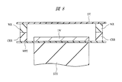
After the back surface grinding of the
まず、図8に示すように、たとえばポリオレフィン等の樹脂からなり、ウエハ1Wより大きな径を有し、厚さが100μm程度のダイシングテープDTを用意する。このダイシングテープDTは片面が粘着面(第2の粘着面)となっており、この粘着面には予めキャリアリングCRRと同程度の内径(内周(第2の内周))および外径(外周(第2の外周))を有するウエハリング(第2の搬送治具)WRの第3の主面が貼付されている。このウエハリングWRは、たとえばステンレスから形成されており、前記第3の主面とは反対側の第4の主面を有する。続いて、ウエハ1Wを固定したウエハ保護テープWPTが、ウエハ1Wの径以上かつキャリアリングCRRおよびウエハリングWRの内径以下の径を有するステージSTGに真空吸着された状態で、ダイシングテープDTに貼付されたウエハリングWRがキャリアリングCRRと対向するように貼り合わせる。
First, as shown in FIG. 8, a dicing tape DT made of a resin such as polyolefin and having a diameter larger than that of the
次に、図9に示すように、ウエハ1Wの径以上かつキャリアリングCRRおよびウエハリングWRの内径以下の径を有するステージSTGを用い、ウエハ1WをダイシングテープDTの粘着面に押し付けるように、キャリアリングCRRおよびウエハリングWRを下方向(ステージ側)に押し下げることでウエハ保護テープWPTおよびウエハ1Wを突き上げ、ウエハ1Wの裏面をダイシングテープDTの粘着面に貼付する。
Next, as shown in FIG. 9, using a stage STG having a diameter equal to or larger than the diameter of the
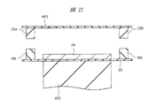
次に、図10に示すように、ウエハ1Wの主面がウエハ保護テープWPTに貼付られ、かつウエハ1Wの裏面がダイシングテープDTの粘着面に貼付された状態で上下反転し、ダイシングテープDTをステージSTG上に吸着保持する。
Next, as shown in FIG. 10, the dicing tape DT is turned upside down with the main surface of the
そして、図11に示すように、ウエハ保護テープWPTをウエハ1Wの主面から剥離し、キャリアリングCRRとウエハリングWRとを剥離することによって、ウエハ1Wの裏面へのダイシングテープDTの貼付工程は完了する。
Then, as shown in FIG. 11, the wafer protection tape WPT is peeled off from the main surface of the
このようなウエハ1Wの裏面へのダイシングテープDTの貼付工程によれば、ウエハ1Wの搬送時にウエハ1Wに外部からの衝撃や力が伝わることを防いでいたキャリアリングCRRを介してウエハ1Wの裏面へダイシングテープDTを貼付することができる。それにより、薄型化によって機械的強度が低下しているウエハ1Wに直接ストレスを与えることなくウエハ1Wの裏面にダイシングテープDTを貼付することが可能となるので、ダイシングテープDTの貼付時にウエハ1Wに割れや欠けが発生してしまうことを防ぐことができる。また、ウエハ保護テープWPTおよびキャリアリングCRRの剥離後は、キャリアリングCRRを用いずにウエハ1Wの搬送および裏面研削を行う場合と同様の形態となるので、ダイシング工程以降はキャリアリングCRRを用いずにウエハ1Wの搬送および裏面研削を行う場合の設備をそのまま利用することができる。
According to the affixing process of the dicing tape DT to the back surface of the
上記図8〜図11を用いて説明したような工程によってウエハ1Wの裏面へのダイシングテープDTを貼付する代わりに、以下の図12〜図13を用いて説明する工程によってウエハ1Wの裏面へのダイシングテープDTを貼付してもよい。
Instead of applying the dicing tape DT to the back surface of the
まず、図12に示すように、図8に示したダイシングテープDTを用意する。ダイシングテープDTの粘着面には、予めウエハリングWR2を貼付しておくが、このウエハリングWR2は、キャリアリングCRRの内径より小さな外径とウエハ1Wの径より大きな内径を有するものである。続いて、ウエハリングWR2がダイシングテープDTに貼付されている状況下で、ウエハリングWR2がウエハ1Wを取り囲むようにウエハリングWR2をウエハ保護テープWPTに貼付する。
First, as shown in FIG. 12, the dicing tape DT shown in FIG. 8 is prepared. Wafer ring WR2 is affixed in advance to the adhesive surface of dicing tape DT. Wafer ring WR2 has an outer diameter smaller than the inner diameter of carrier ring CRR and an inner diameter larger than the diameter of
次に、図13に示すように、前述の図9で示したステージSTGを用い、ウエハ1WをダイシングテープDTの粘着面に押し付けるようにウエハ保護テープWPTおよびウエハ1Wを突き上げ、ウエハ1Wの裏面をダイシングテープDTの粘着面に貼付する。
Next, as shown in FIG. 13, using the stage STG shown in FIG. 9, the wafer protective tape WPT and the
次に、図14に示すように、ウエハ保護テープWPTをウエハ1Wの主面から剥離し、ウエハリングWR2をウエハ保護テープWPTから剥離することによって、ウエハ1Wの裏面へのダイシングテープDTの貼付工程は完了する。
Next, as shown in FIG. 14, the wafer protection tape WPT is peeled off from the main surface of the
また、ウエハリングWR、WR2を用いずに、以下の図15〜図17を用いて説明する工程によってウエハ1Wの裏面へのダイシングテープDTを貼付してもよい。
Further, the dicing tape DT may be affixed to the back surface of the
まず、図15に示すように、図8に示したダイシングテープDTを用意する。この時、ダイシングテープDTの粘着面には、ウエハリングWR、WR2は貼付されていない。続いて、ダイシングテープDTをキャリアリングCRRの上面に貼付する。 First, as shown in FIG. 15, the dicing tape DT shown in FIG. 8 is prepared. At this time, the wafer rings WR and WR2 are not attached to the adhesive surface of the dicing tape DT. Subsequently, the dicing tape DT is attached to the upper surface of the carrier ring CRR.
次に、図16に示すように、前述の図9で示したステージSTGを用い、ウエハ1WをダイシングテープDTの粘着面に押し付けるようにウエハ保護テープWPTおよびウエハ1Wを突き上げ、ウエハ1Wの裏面をダイシングテープDTの粘着面に貼付する。
Next, as shown in FIG. 16, using the stage STG shown in FIG. 9, the wafer protective tape WPT and the
次に、図17に示すように、ウエハ保護テープWPTをウエハ1Wの主面から剥離し、キャリアリングCRRをウエハ保護テープWPTから剥離することによって、ウエハ1Wの裏面へのダイシングテープDTの貼付工程は完了する。ウエハ保護テープWPTの剥離後においては、キャリアリングCRRが前述のウエハリングWR、WR2と同様の機能を果たす。
Next, as shown in FIG. 17, the wafer protection tape WPT is peeled off from the main surface of the
ウエハ1Wを個々のチップ1Cへ分割した後、図18に示すように、チップ搭載用の実装基板11を用意する。この実装基板11は、たとえばエポキシ樹脂(ガラス・エポキシ樹脂)のような汎用樹脂を主体として形成された多層配線基板である。すなわち、表面や裏面に配線を印刷法で形成した、いわゆるプリント基板を複数積層した構造となっており、この複数層のプリント基板の各配線は、各プリント基板に形成されたビアホールを通じて電気的に接続されている。また、実装基板11の主面(チップ搭載面)には、複数のボンディングワイヤ接続用のパッドPD1が形成されている。このパッドPD1は、たとえば実装基板11の外周部に沿って配置される。
After the
続いて、その実装基板11上に、接着材塗布領域に対応した平面形状の開口部を有するマスクを、その開口部の位置を接着材塗布領域に合わせて配置する。この時、パッドPD1は、マスクによって覆われる。本実施の形態において、マスクとしては、厚さ30μm程度以下のシルクスクリーンまたはメタルマスクなどを用いることを例示できる。続いて、常温(室温)で、マスクが配置された実装基板11上に接着材14を塗布し、マスクの開口部内に接着材14を埋め込んだ後、実装基板11上からマスクを取り外す。これにより、実装基板11上においては、接着材塗布領域にのみ厚さ30μm程度以下の接着材14を残すことができる。この接着材14は、ペースト状であり、たとえば熱可塑性の樹脂接着材、一部が熱可塑性を有し一部が熱硬化性を有する半熱可塑半熱硬化性の樹脂接着材、または熱硬化性の樹脂接着材などを用いることができる。続いて、たとえば実装基板11に80℃〜200℃程度の熱処理を施すことによって、接着材14を硬化中間状態である、半硬化状態にする。
Subsequently, a mask having a planar opening corresponding to the adhesive application region is arranged on the mounting
次に、図19に示すように、常温(室温)〜200℃程度の雰囲気中にて、チップ1Cを接着材14に圧着する。チップ6の表面は保護膜で覆われている。また、その保護膜に設けられた複数の開口部からは、それぞれボンディングワイヤ接続用のボンディングパッド(以下、単にパッドと記す)PD2が露出している。パッドPD2は、チップ1C内に形成された最上層配線の一部であり、たとえばチップ1Cの外周部に沿って配置されている。
Next, as shown in FIG. 19, the
次に、図20に示すように、チップ1Cの搭載された実装基板11に80℃〜200℃程度の熱処理を施す。それにより、接着材14を硬化させて、チップ1Cの実装基板11への接着を強固にすることができる。
Next, as shown in FIG. 20, heat treatment at about 80 ° C. to 200 ° C. is performed on the mounting
上記の工程でチップ1Cを実装基板11へ接着する本実施の形態によれば、チップ1Cの厚さが薄い場合でも、チップ1Cを実装基板11へ搭載する時には、接着材14は厚さがチップ1Cより薄く、かつ半硬化した状態となっているので、接着材14がチップ1Cの側面から這い上がり、チップ1Cの上面に付着してしまうことを防ぐことができる。それにより、チップ1Cの耐湿信頼性が低下してしまうことを防ぐことが可能となる。接着材14がチップ1Cの側面から這い上がり、パッドPD2に付着した場合には、後のワイヤボンディング工程でワイヤとパッドPD2との接合不良が発生してしまうことが懸念されるが、本実施の形態によればそのような不具合も防ぐことができる。
According to the present embodiment in which the
また、パッケージの小型化に伴って、チップ1Cと実装基板11上に形成されたパッドPD1との間の距離が小さくなっている場合には、粘性の低いペースト状の接着材を用いてチップ1Cと実装基板11とを接着すると、接着材が実装基板11上に広がり、パッドPD1に付着してしまう不具合が懸念される。一方、上記の本実施の形態のように、チップ1Cの接着時において、接着材14をチップ1Cより薄くし、かつ印刷による塗布時に比較べて粘性の高い半硬化状態としておくことによって、そのような不具合を防ぐことができる。それにより、後のワイヤボンディング工程でワイヤとパッドPD1との接合不良が発生してしまうことを防ぐことが可能になる。
In addition, when the distance between the
また、チップ1Cの厚さが薄くなるに従って、チップ1Cの主面(素子形成面)に形成された部材とその下部の部材との熱膨張率の差等に起因する応力の差が生じ、チップ1Cの反りが大きくなる。このように反ってしまったチップ1Cを、たとえば熱硬化性樹脂接着材で接着しようとすると、チップ1Cが反ったままの状態で熱硬化性樹脂接着材が硬化してしまい、チップ1Cの接着面の全面で均一な接着材の濡れ性を確保できなくなり、接着不良を引き起こしてしまう不具合が懸念される。チップ1Cの接着面の全面で均一な接着材の濡れ性が確保できない場合には、チップ1Cの接着面に気泡を含んで接着材が硬化してしまう虞があり、この気泡が後のリフロー工程時に膨張してチップ1Cが割れてしまう不具合も懸念される。一方、上記の本実施の形態の接着手段では、チップ1Cが反っている場合でも、熱圧着することによって、接着後においてチップ1Cを平坦な状態で固定できる。それにより、チップ1Cの接着面の全面で均一な接着材の濡れ性を確保し、チップ1Cを平坦な状態で実装基板11に接着することができる。それにより、前述したチップ1Cの接着不良および割れといった不具合を防ぐことができる。
Further, as the thickness of the
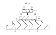
次に、図21に示すように、裏面にフィルム状の接着材17が貼付されたチップ18を用意する。チップ18は、個々のチップ18へ分割される前のウエハ状態の時に、チップ1Cとなったウエハ1Wと同様の裏面研削処理が施され、薄型化されている。チップ18の裏面へ接着材17を貼り付けるには、たとえばウエハを個々のチップ18へ分割する前に、そのウエハの裏面を研削して所定の厚さにした後、ウエハの裏面全面に熱可塑性のフィルム状の接着材17を貼付し、その後、接着材17ごとウエハを個々のチップ18へ分割することで実現できる。また、チップ18の表面は保護膜で覆われている。その保護膜に設けられた複数の開口部からは、それぞれボンディングワイヤ接続用のパッドPD3が露出している。パッドPD3は、チップ18内に形成された最上層配線の一部であり、たとえばチップ18の外周部に沿って配置されている。
Next, as shown in FIG. 21, a
続いて、チップ1Cが接着された実装基板11を加熱ステージHS上に配置し、100℃〜200℃程度の温度で加熱する。その状態で、チップ1C上に上記接着材17を介してチップ18を熱圧着する。チップ18の接着に熱可塑性のフィルム状の接着材17を用いることにより、接着材17がチップ18の側面から這い上がり、チップ18の上面に付着してしまうことを防ぐことができる。それにより、チップ18の耐湿信頼性が低下してしまうことを防ぐことが可能となる。接着材17がチップ18の側面から這い上がり、パッドPD13に付着した場合には、後のワイヤボンディング工程でワイヤとパッドPD3との接合不良が発生してしまうことが懸念されるが、本実施の形態によればそのような不具合も防ぐことができる。また、パッケージの小型化に伴って、チップ18とチップ1Cに形成されたパッドPD2との間の距離が小さくなっている場合においても、接着材17がチップ1C上に広がってパッドPD2に付着してしまうような不具合を防ぐことができる。それにより、後のワイヤボンディング工程でワイヤとパッドPD2との接合不良が発生してしまうことを防ぐことが可能になる。
Subsequently, the mounting
また、前述したチップ1Cの場合と同様に、チップ18が接着時に反っている場合でも、チップ1Cへの接着は熱圧着により行われるので、接着後においてチップ18を平坦な状態で固定できる。
Similarly to the case of the
続いて、チップ1C、18の搭載された実装基板11に80℃〜200℃程度の熱処理を施す。それにより、接着材17を硬化させて、チップ18のチップ1Cへの接着を強固にすることができる。
Subsequently, a heat treatment at about 80 ° C. to 200 ° C. is performed on the mounting
次に、図22に示すように、実装基板11を加熱ステージHS上に搭載し、約100℃〜250℃で加熱しながら、実装基板11上のパッドPD1とチップ1CのパッドPD2とをワイヤ19で電気的に接続(ワイヤボンディング)し、実装基板11上のパッドPD1とチップ18のパッドPD3とをワイヤ20で電気的に接続する。本実施の形態において、ワイヤ19、20は、Au(金)などの導電性材料とすることを例示でき、ワイヤボンディング処理は、超音波振動と熱圧着とを併用したワイヤボンダを使用して行うことを例示できる。
Next, as illustrated in FIG. 22, the mounting
次に、図23に示すように、実装基板11、チップ1C、18、およびワイヤ19、20を金型(図示は省略)で挟持し、その金型のキャビティ内に150℃〜200℃程度で溶融したモールド樹脂21を注入し、実装基板11、チップ1C、18、およびワイヤ19、20をそのモールド樹脂21によって封止する。金型のキャビティ内へのモールド樹脂21の注入時には、金型もモールド樹脂21と同程度の温度で加熱しておく。また、図19を用いて説明した熱処理工程および図20を用いて説明した熱処理工程における温度条件が、このモールド樹脂21による封止工程時の温度と合致する場合には、前述の熱処理をこの封止工程時の熱を利用して一括して行ってもよい。
Next, as shown in FIG. 23, the mounting
次に、図24に示すように、実装基板11側を上面とし、実装基板11上にバンプ電極22を形成する。このバンプ電極22は、たとえばSn(スズ)−Ag(銀)−Cu(銅)共晶合金から形成されたはんだボールを実装基板11の上面(チップ搭載側の逆側)に供給した後、実装基板11等を240℃〜260℃の雰囲気中に配置し、はんだボールをリフローすることで形成することができる。その後、図25に示すように、バンプ電極22の形成面を下側とし、本実施の形態の半導体装置が略完成する。
Next, as shown in FIG. 24, the
上記の工程によって形成された本実施の形態の半導体装置(半導体パッケージ)は、下層のチップ1CをDRAM(Dynamic Random Access Memory)等のメモリ回路が形成されたチップとし、上層のチップ18をチップ1Cに形成されたメモリ回路の動作を制御するコントローラ(CPU)が形成されたチップとすることができる。前述したウエハ1Wの薄型化が実現できない場合において、半導体パッケージの高さに制限があると、メモリ回路が形成されたチップとコントローラが形成されたチップとは、それぞれ別個に半導体パッケージにする必要が生じ、これら半導体パッケージを実装する領域が広くなってしまう不具合が生じる。一方、本実施の形態によれば、ウエハ1Wの薄型化を実現できるので、2個のチップを積層しても半導体パッケージの高さを低く抑えることが可能となり、たとえば各チップ毎に別個に半導体パッケージを形成した場合と同程度にまで高さを抑制することができる。それにより、半導体パッケージの実装領域を縮小できるので、半導体パッケージが実装されるモジュールの小型化を実現できる。
In the semiconductor device (semiconductor package) of the present embodiment formed by the above process, the
ところで、上記の本実施の形態では、チップを2段に積層する例について説明したが、さらに多段に積層してもよい。たとえば、図26に示すように、チップ18をチップ1Cに積層した手段と同様の手段により、チップ23をチップ18に積層する。すなわち、接着材17と同様の熱可塑性のフィルム状の接着材25を用いてチップ23をチップ18に熱圧着し、ワイヤ19、20と同様のワイヤ26によって、チップ23に形成されたパッドPD4と実装基板11上のパッドPD1とを電気的に接続するものである。
In the above-described embodiment, an example in which chips are stacked in two stages has been described. However, the chips may be stacked in more stages. For example, as shown in FIG. 26, the
以上、本発明者によってなされた発明を実施の形態に基づき具体的に説明したが、本発明は前記実施の形態に限定されるものではなく、その要旨を逸脱しない範囲で種々変更可能であることはいうまでもない。 As mentioned above, the invention made by the present inventor has been specifically described based on the embodiment. However, the present invention is not limited to the embodiment, and various modifications can be made without departing from the scope of the invention. Needless to say.
前記実施の形態では、薄型化された単結晶シリコン等から形成されたウエハをキャリアリングを用いて搬送する場合について説明したが、相対的に単結晶シリコン等から形成されたウエハより機械的強度が低いガリウムヒ素から形成されたウエハでもキャリアリングを用いて搬送することにより、ウエハの割れや欠けを防ぐことができる。 In the above-described embodiment, the case where a wafer formed of thinned single crystal silicon or the like is transported using a carrier ring has been described. However, the mechanical strength is relatively higher than that of a wafer formed of single crystal silicon or the like. Wafers formed from low gallium arsenide can be prevented from being cracked or chipped by being conveyed using carrier rings.
本発明の半導体装置の製造方法は、たとえば薄型化したウエハを用いて製造する半導体パッケージの製造工程に適用することができる。 The semiconductor device manufacturing method of the present invention can be applied to a manufacturing process of a semiconductor package manufactured using, for example, a thinned wafer.
1C チップ(チップ領域)
1W ウエハ
11 実装基板
14 接着材
17 接着材
18 チップ
19、20 ワイヤ
21 モールド樹脂
22 バンプ電極
23 チップ
25 接着材
26 ワイヤ
CR 切断領域(分離領域)
CRR キャリアリング(第1の搬送治具)
DT ダイシングテープ
GW グラインディングホイール(研削手段)
HS 加熱ステージ
KS1 保持面(ウエハ保持面、第1の吸着面)
KS2 保持面(第2の吸着面)
KT 保持具(第1の固定手段)
KTU 上端部
N ノッチ
PD1、PD2、PD3、PD4 パッド
RA1 回転軸
RS1 裏面
STG ステージ
US1 上面
WPT ウエハ保護テープ(保護テープ)
WR、WR2 ウエハリング(第2の搬送治具)
WSG ウエハステージ(ウエハ保持手段)
1C chip (chip area)
CRR carrier ring (first transfer jig)
DT Dicing tape GW Grinding wheel (grinding means)
HS Heating stage KS1 Holding surface (wafer holding surface, first suction surface)
KS2 holding surface (second suction surface)
KT holder (first fixing means)
KTU Upper end N Notch PD1, PD2, PD3, PD4 Pad RA1 Rotating shaft RS1 Back surface STG Stage US1 Upper surface WPT Wafer protective tape (protective tape)
WR, WR2 Wafer ring (second transfer jig)
WSG wafer stage (wafer holding means)
Claims (9)
(b)前記(a)工程の後、平面視においてリング状の第1搬送治具の内周が前記半導体ウエハの外周を取り囲むように前記第1搬送治具の第2主面が前記保護テープに固定された状態で、前記半導体ウエハの前記第1裏面を研削する工程、
(c)前記(b)工程の後、前記半導体ウエハの前記第1裏面側にダイシングテープを固定する工程、
(d)前記(c)工程の後、前記保護テープのうちの前記半導体ウエハの前記第1主面と対向する面とは反対側の面に前記第1搬送治具の前記内周以下の径を有するステージを押し付けることで前記半導体ウエハの前記第1裏面に前記ダイシングテープを貼り付け、前記半導体ウエハの前記第1主面と前記第1搬送治具の前記第2主面から前記保護テープを剥離する工程、
(e)前記(d)工程の後、前記半導体ウエハの前記分割領域に沿って、前記半導体ウエハを分割する工程、
を含み、
前記(c)工程では、前記半導体ウエハの前記第1裏面に前記ダイシングテープが貼り付けられていないことを特徴とする半導体装置の製造方法。 (A) A protective tape is affixed to the first main surface of a semiconductor wafer having a first main surface in which a plurality of chip regions are defined by divided regions and a first back surface opposite to the first main surface. Process,
(B) After the step (a) , the second main surface of the first transfer jig is the protective tape so that the inner periphery of the ring-shaped first transfer jig surrounds the outer periphery of the semiconductor wafer in plan view. A step of grinding the first back surface of the semiconductor wafer while being fixed to
(C) After the step (b), a step of fixing a dicing tape to the first back side of the semiconductor wafer;
(D) After the step (c), a diameter equal to or smaller than the inner circumference of the first transfer jig on the surface of the protective tape opposite to the surface facing the first main surface of the semiconductor wafer. paste the dicing tape to the first back surface of the semiconductor wafer by pressing the stages having attached, said first major surface and said second major surface or found before SL protection of the first transfer jig of the semiconductor wafer A step of peeling the tape,
(E) After the step (d) , dividing the semiconductor wafer along the divided region of the semiconductor wafer;
Only including,
In the step (c), the dicing tape is not attached to the first back surface of the semiconductor wafer .
前記半導体ウエハの前記複数のチップ領域のそれぞれには、半導体素子が形成されていることを特徴とする半導体装置の製造方法。 In claim 1,
A semiconductor device manufacturing method, wherein a semiconductor element is formed in each of the plurality of chip regions of the semiconductor wafer.
前記(b)工程では、前記半導体ウエハが固定された前記保護テープをウエハステージ上に配置し、前記保護テープに固定され、前記半導体ウエハの厚さよりも厚く形成された前記第1搬送治具の前記第2裏面を前記半導体ウエハの前記第1裏面より低くし、グラインディングホイールを用いて前記半導体ウエハの前記第1裏面を研削することを特徴とする半導体装置の製造方法。 In claim 1,
Wherein in the step (b), the protective tape in which the semiconductor wafer is fixed arranged on a wafer stage, it is fixed to the protective tape, the semiconductor wafer thickness formed of the first transfer jig thicker than A method of manufacturing a semiconductor device, wherein the second back surface is made lower than the first back surface of the semiconductor wafer, and the first back surface of the semiconductor wafer is ground using a grinding wheel.
前記(b)工程では、回転する前記グラインディングホイールを、回転する前記ウエハステージ上に配置された前記半導体ウエハの一部と前記第1搬送治具の一部を覆うように接触させることで、前記半導体ウエハの前記第1裏面を研削することを特徴とする半導体装置の製造方法。 In claim 3,
In the step (b), the rotating grinding wheel is brought into contact so as to cover a part of the semiconductor wafer disposed on the rotating wafer stage and a part of the first transfer jig, A method of manufacturing a semiconductor device, comprising grinding the first back surface of the semiconductor wafer.
前記ウエハステージは、前記半導体ウエハの下側に位置する第1保持面と、前記第1保持面よりも低く、前記第1搬送治具の下側に位置する第2保持面とを有し、
前記第1搬送治具を前記第2保持面に向かって引き下げることで、前記第1搬送治具の前記第2裏面を前記半導体ウエハの前記第1裏面より低くすることを特徴とする半導体装置の製造方法。 In claim 4,
The wafer stage has a first holding surface located below the semiconductor wafer, and a second holding surface located below the first transfer jig and lower than the first holding surface,
By lowering the first transfer jig toward the second holding surface, of the semiconductor device, characterized by the second back surface of the first transfer jig lower than the first back surface of the semiconductor wafer Production method.
前記保護テープは、前記ウエハステージの前記第1保持面に吸着されていることを特徴とする半導体装置の製造方法。 In claim 5,
The method for manufacturing a semiconductor device, wherein the protective tape is adsorbed to the first holding surface of the wafer stage.
前記ウエハステージの前記第1保持面は、傾斜していることを特徴とする半導体装置の製造方法。 In claim 5,
The method of manufacturing a semiconductor device, wherein the first holding surface of the wafer stage is inclined.
前記(c)工程では、前記半導体ウエハの前記第1裏面に前記ダイシングテープが貼り付かないように、前記第1搬送治具の前記第2裏面に前記ダイシングテープを貼り付けて固定することを特徴とする半導体装置の製造方法。 In claim 1,
In the step (c), the dicing tape is attached and fixed to the second back surface of the first transport jig so that the dicing tape is not attached to the first back surface of the semiconductor wafer. A method for manufacturing a semiconductor device.
前記(c)工程では、前記半導体ウエハの前記第1裏面に前記ダイシングテープが貼り付かないように、前記ダイシングテープに固定された第2搬送治具を前記第1搬送治具の前記第2裏面に接触させることを特徴とする半導体装置の製造方法。In the step (c), a second transport jig fixed to the dicing tape is used as the second back surface of the first transport jig so that the dicing tape does not adhere to the first back surface of the semiconductor wafer. A method for manufacturing a semiconductor device, comprising: contacting with a semiconductor device.
Priority Applications (1)
| Application Number | Priority Date | Filing Date | Title |
|---|---|---|---|
| JP2005231473A JP4848153B2 (en) | 2005-08-10 | 2005-08-10 | Manufacturing method of semiconductor device |
Applications Claiming Priority (1)
| Application Number | Priority Date | Filing Date | Title |
|---|---|---|---|
| JP2005231473A JP4848153B2 (en) | 2005-08-10 | 2005-08-10 | Manufacturing method of semiconductor device |
Publications (3)
| Publication Number | Publication Date |
|---|---|
| JP2007048920A JP2007048920A (en) | 2007-02-22 |
| JP2007048920A5 JP2007048920A5 (en) | 2008-09-18 |
| JP4848153B2 true JP4848153B2 (en) | 2011-12-28 |
Family
ID=37851506
Family Applications (1)
| Application Number | Title | Priority Date | Filing Date |
|---|---|---|---|
| JP2005231473A Expired - Fee Related JP4848153B2 (en) | 2005-08-10 | 2005-08-10 | Manufacturing method of semiconductor device |
Country Status (1)
| Country | Link |
|---|---|
| JP (1) | JP4848153B2 (en) |
Families Citing this family (16)
| Publication number | Priority date | Publication date | Assignee | Title |
|---|---|---|---|---|
| DE102006000687B4 (en) | 2006-01-03 | 2010-09-09 | Thallner, Erich, Dipl.-Ing. | Combination of a carrier and a wafer, device for separating the combination and methods for handling a carrier and a wafer |
| JP2007294748A (en) * | 2006-04-26 | 2007-11-08 | Tokyo Seimitsu Co Ltd | Wafer transporting method |
| JP4729003B2 (en) * | 2007-06-08 | 2011-07-20 | リンテック株式会社 | Processing method for brittle members |
| JP5276823B2 (en) * | 2007-10-04 | 2013-08-28 | 株式会社ディスコ | Wafer grinding equipment |
| JP5272397B2 (en) * | 2007-12-13 | 2013-08-28 | 日立化成株式会社 | Adhesive film application apparatus and adhesive film application method |
| JP5253996B2 (en) * | 2008-12-26 | 2013-07-31 | 株式会社ディスコ | Work dividing method and tape expansion device |
| EP2660851B1 (en) | 2009-03-18 | 2020-10-14 | EV Group GmbH | Device and method for releasing a wafer from a holder |
| JP5415181B2 (en) * | 2009-08-19 | 2014-02-12 | 株式会社ディスコ | Wafer grinding equipment |
| EP2706561B1 (en) | 2009-09-01 | 2017-04-05 | EV Group GmbH | Method for concentrically releasing a product substrate (e.g., a semiconductor wafer) from a support substrate by deformation of a flexible film mounted on a frame |
| EP2381464B1 (en) | 2010-04-23 | 2012-09-05 | EV Group GmbH | Device and method for releasing a product substrate from a holder substrate |
| JP2012160515A (en) * | 2011-01-31 | 2012-08-23 | Disco Abrasive Syst Ltd | Workpiece processing method |
| JP6087565B2 (en) * | 2012-10-03 | 2017-03-01 | 株式会社ディスコ | Grinding apparatus and grinding method |
| JP5580439B2 (en) * | 2013-01-29 | 2014-08-27 | アギア システムズ インコーポレーテッド | Method for separating a semiconductor wafer into individual semiconductor dies using implanted impurities |
| JP6822857B2 (en) * | 2017-01-17 | 2021-01-27 | 株式会社ディスコ | Carry-out mechanism |
| KR102642079B1 (en) * | 2018-02-07 | 2024-02-28 | 린텍 가부시키가이샤 | Adhesive tape for semiconductor processing |
| KR20200102612A (en) * | 2019-02-21 | 2020-09-01 | 세메스 주식회사 | Substrate treating apparatus and substrate treating method |
Family Cites Families (3)
| Publication number | Priority date | Publication date | Assignee | Title |
|---|---|---|---|---|
| JP3097619B2 (en) * | 1997-10-02 | 2000-10-10 | 日本電気株式会社 | Method of manufacturing field emission cold cathode |
| JP4731050B2 (en) * | 2001-06-15 | 2011-07-20 | 株式会社ディスコ | Processing method of semiconductor wafer |
| JP4152295B2 (en) * | 2003-10-23 | 2008-09-17 | Necエンジニアリング株式会社 | Tape applicator |
-
2005
- 2005-08-10 JP JP2005231473A patent/JP4848153B2/en not_active Expired - Fee Related
Also Published As
| Publication number | Publication date |
|---|---|
| JP2007048920A (en) | 2007-02-22 |
Similar Documents
| Publication | Publication Date | Title |
|---|---|---|
| JP4848153B2 (en) | Manufacturing method of semiconductor device | |
| TWI284960B (en) | Manufacturing method of semiconductor device | |
| TWI420640B (en) | Semiconductor package device, semiconductor package structure, and method for fabricating the same | |
| JP3701542B2 (en) | Semiconductor device and manufacturing method thereof | |
| KR100517075B1 (en) | Method for manufacturing semiconductor device | |
| US8394677B2 (en) | Method of fabricating semiconductor device | |
| JP5798834B2 (en) | Manufacturing method of semiconductor device | |
| US20070275543A1 (en) | Manufacturing method of a semiconductor device | |
| JP4992904B2 (en) | Manufacturing method of semiconductor device | |
| US8546244B2 (en) | Method of manufacturing semiconductor device | |
| TWI733049B (en) | Semiconductor package and manufacturing method thereof | |
| US20050208734A1 (en) | Thin flip-chip method | |
| JP2001168275A (en) | Small integrated circuit package and its manufacturing method | |
| JPWO2008038345A6 (en) | Manufacturing method of semiconductor device | |
| JP2001338932A (en) | Semiconductor device and method of manufacturing semiconductor device | |
| JP2010010174A (en) | Method for manufacturing semiconductor device | |
| US20050196901A1 (en) | Device mounting method and device transport apparatus | |
| JP4057875B2 (en) | Manufacturing method of semiconductor device | |
| JP5286303B2 (en) | Manufacturing method of semiconductor device | |
| JP5054954B2 (en) | Manufacturing method of semiconductor device | |
| JP3621908B2 (en) | Bare chip mounting method and mounting system | |
| US20070114672A1 (en) | Semiconductor device and method of manufacturing the same | |
| JP2007134489A (en) | Semiconductor device and method for manufacturing same | |
| JP4483136B2 (en) | Semiconductor device mounting method and semiconductor device manufacturing method | |
| US20100289129A1 (en) | Copper plate bonding for high performance semiconductor packaging |
Legal Events
| Date | Code | Title | Description |
|---|---|---|---|
| A521 | Written amendment |
Free format text: JAPANESE INTERMEDIATE CODE: A523 Effective date: 20080806 |
|
| A621 | Written request for application examination |
Free format text: JAPANESE INTERMEDIATE CODE: A621 Effective date: 20080806 |
|
| A711 | Notification of change in applicant |
Free format text: JAPANESE INTERMEDIATE CODE: A712 Effective date: 20100528 |
|
| A977 | Report on retrieval |
Free format text: JAPANESE INTERMEDIATE CODE: A971007 Effective date: 20110224 |
|
| A131 | Notification of reasons for refusal |
Free format text: JAPANESE INTERMEDIATE CODE: A131 Effective date: 20110301 |
|
| A521 | Written amendment |
Free format text: JAPANESE INTERMEDIATE CODE: A523 Effective date: 20110427 |
|
| TRDD | Decision of grant or rejection written | ||
| A01 | Written decision to grant a patent or to grant a registration (utility model) |
Free format text: JAPANESE INTERMEDIATE CODE: A01 Effective date: 20110920 |
|
| A01 | Written decision to grant a patent or to grant a registration (utility model) |
Free format text: JAPANESE INTERMEDIATE CODE: A01 |
|
| A61 | First payment of annual fees (during grant procedure) |
Free format text: JAPANESE INTERMEDIATE CODE: A61 Effective date: 20111017 |
|
| FPAY | Renewal fee payment (event date is renewal date of database) |
Free format text: PAYMENT UNTIL: 20141021 Year of fee payment: 3 |
|
| R150 | Certificate of patent or registration of utility model |
Free format text: JAPANESE INTERMEDIATE CODE: R150 |
|
| S531 | Written request for registration of change of domicile |
Free format text: JAPANESE INTERMEDIATE CODE: R313531 |
|
| R350 | Written notification of registration of transfer |
Free format text: JAPANESE INTERMEDIATE CODE: R350 |
|
| LAPS | Cancellation because of no payment of annual fees |