EP1463026B1 - Signal line drive circuit and light emitting device - Google Patents
Signal line drive circuit and light emitting device Download PDFInfo
- Publication number
- EP1463026B1 EP1463026B1 EP02775442A EP02775442A EP1463026B1 EP 1463026 B1 EP1463026 B1 EP 1463026B1 EP 02775442 A EP02775442 A EP 02775442A EP 02775442 A EP02775442 A EP 02775442A EP 1463026 B1 EP1463026 B1 EP 1463026B1
- Authority
- EP
- European Patent Office
- Prior art keywords
- current
- current source
- circuit
- transistor
- signal
- Prior art date
- Legal status (The legal status is an assumption and is not a legal conclusion. Google has not performed a legal analysis and makes no representation as to the accuracy of the status listed.)
- Expired - Lifetime
Links
- 238000005070 sampling Methods 0.000 claims abstract description 33
- 229910021420 polycrystalline silicon Inorganic materials 0.000 claims description 6
- 229920005591 polysilicon Polymers 0.000 claims description 6
- 239000011159 matrix material Substances 0.000 claims description 2
- 238000000034 method Methods 0.000 abstract description 83
- 239000003990 capacitor Substances 0.000 description 85
- 238000010586 diagram Methods 0.000 description 36
- 239000006185 dispersion Substances 0.000 description 30
- 239000000463 material Substances 0.000 description 23
- 230000000717 retained effect Effects 0.000 description 23
- 239000010410 layer Substances 0.000 description 19
- 239000000758 substrate Substances 0.000 description 18
- 238000006243 chemical reaction Methods 0.000 description 17
- 238000009825 accumulation Methods 0.000 description 13
- 239000000126 substance Substances 0.000 description 13
- 230000000694 effects Effects 0.000 description 12
- CNQCVBJFEGMYDW-UHFFFAOYSA-N lawrencium atom Chemical compound [Lr] CNQCVBJFEGMYDW-UHFFFAOYSA-N 0.000 description 9
- 239000003566 sealing material Substances 0.000 description 8
- IJGRMHOSHXDMSA-UHFFFAOYSA-N Atomic nitrogen Chemical compound N#N IJGRMHOSHXDMSA-UHFFFAOYSA-N 0.000 description 6
- 239000004973 liquid crystal related substance Substances 0.000 description 6
- 239000004065 semiconductor Substances 0.000 description 6
- XLOMVQKBTHCTTD-UHFFFAOYSA-N Zinc monoxide Chemical compound [Zn]=O XLOMVQKBTHCTTD-UHFFFAOYSA-N 0.000 description 4
- 230000003247 decreasing effect Effects 0.000 description 4
- 239000000945 filler Substances 0.000 description 4
- QVGXLLKOCUKJST-UHFFFAOYSA-N atomic oxygen Chemical compound [O] QVGXLLKOCUKJST-UHFFFAOYSA-N 0.000 description 3
- 230000008859 change Effects 0.000 description 3
- 230000007423 decrease Effects 0.000 description 3
- 229910003437 indium oxide Inorganic materials 0.000 description 3
- PJXISJQVUVHSOJ-UHFFFAOYSA-N indium(iii) oxide Chemical compound [O-2].[O-2].[O-2].[In+3].[In+3] PJXISJQVUVHSOJ-UHFFFAOYSA-N 0.000 description 3
- 239000001301 oxygen Substances 0.000 description 3
- 229910052760 oxygen Inorganic materials 0.000 description 3
- 229920003023 plastic Polymers 0.000 description 3
- 239000004033 plastic Substances 0.000 description 3
- 229920002620 polyvinyl fluoride Polymers 0.000 description 3
- 229920005989 resin Polymers 0.000 description 3
- 239000011347 resin Substances 0.000 description 3
- 230000004044 response Effects 0.000 description 3
- XKRFYHLGVUSROY-UHFFFAOYSA-N Argon Chemical compound [Ar] XKRFYHLGVUSROY-UHFFFAOYSA-N 0.000 description 2
- 229920002799 BoPET Polymers 0.000 description 2
- 239000005041 Mylar™ Substances 0.000 description 2
- NIXOWILDQLNWCW-UHFFFAOYSA-N acrylic acid group Chemical group C(C=C)(=O)O NIXOWILDQLNWCW-UHFFFAOYSA-N 0.000 description 2
- 229910052782 aluminium Inorganic materials 0.000 description 2
- XAGFODPZIPBFFR-UHFFFAOYSA-N aluminium Chemical compound [Al] XAGFODPZIPBFFR-UHFFFAOYSA-N 0.000 description 2
- QVQLCTNNEUAWMS-UHFFFAOYSA-N barium oxide Chemical compound [Ba]=O QVQLCTNNEUAWMS-UHFFFAOYSA-N 0.000 description 2
- DQXBYHZEEUGOBF-UHFFFAOYSA-N but-3-enoic acid;ethene Chemical compound C=C.OC(=O)CC=C DQXBYHZEEUGOBF-UHFFFAOYSA-N 0.000 description 2
- 238000004891 communication Methods 0.000 description 2
- 150000001875 compounds Chemical class 0.000 description 2
- 239000011231 conductive filler Substances 0.000 description 2
- 238000000151 deposition Methods 0.000 description 2
- 230000008021 deposition Effects 0.000 description 2
- 230000006866 deterioration Effects 0.000 description 2
- 239000005038 ethylene vinyl acetate Substances 0.000 description 2
- 230000005281 excited state Effects 0.000 description 2
- 239000011152 fibreglass Substances 0.000 description 2
- 239000011521 glass Substances 0.000 description 2
- 238000002347 injection Methods 0.000 description 2
- 239000007924 injection Substances 0.000 description 2
- 229910052757 nitrogen Inorganic materials 0.000 description 2
- 229920001200 poly(ethylene-vinyl acetate) Polymers 0.000 description 2
- 229920002037 poly(vinyl butyral) polymer Polymers 0.000 description 2
- 229920006267 polyester film Polymers 0.000 description 2
- 229920000915 polyvinyl chloride Polymers 0.000 description 2
- 239000004800 polyvinyl chloride Substances 0.000 description 2
- 230000001681 protective effect Effects 0.000 description 2
- 230000002829 reductive effect Effects 0.000 description 2
- 238000009877 rendering Methods 0.000 description 2
- 230000002441 reversible effect Effects 0.000 description 2
- 239000002356 single layer Substances 0.000 description 2
- 230000001629 suppression Effects 0.000 description 2
- XOLBLPGZBRYERU-UHFFFAOYSA-N tin dioxide Chemical compound O=[Sn]=O XOLBLPGZBRYERU-UHFFFAOYSA-N 0.000 description 2
- 229910001887 tin oxide Inorganic materials 0.000 description 2
- 239000011787 zinc oxide Substances 0.000 description 2
- 239000004925 Acrylic resin Substances 0.000 description 1
- 229920000178 Acrylic resin Polymers 0.000 description 1
- RYGMFSIKBFXOCR-UHFFFAOYSA-N Copper Chemical compound [Cu] RYGMFSIKBFXOCR-UHFFFAOYSA-N 0.000 description 1
- GYHNNYVSQQEPJS-UHFFFAOYSA-N Gallium Chemical compound [Ga] GYHNNYVSQQEPJS-UHFFFAOYSA-N 0.000 description 1
- 239000004642 Polyimide Substances 0.000 description 1
- XUIMIQQOPSSXEZ-UHFFFAOYSA-N Silicon Chemical compound [Si] XUIMIQQOPSSXEZ-UHFFFAOYSA-N 0.000 description 1
- BQCADISMDOOEFD-UHFFFAOYSA-N Silver Chemical compound [Ag] BQCADISMDOOEFD-UHFFFAOYSA-N 0.000 description 1
- 229910052786 argon Inorganic materials 0.000 description 1
- 230000015572 biosynthetic process Effects 0.000 description 1
- 239000000919 ceramic Substances 0.000 description 1
- 239000011248 coating agent Substances 0.000 description 1
- 238000000576 coating method Methods 0.000 description 1
- 239000000470 constituent Substances 0.000 description 1
- 229910052802 copper Inorganic materials 0.000 description 1
- 239000010949 copper Substances 0.000 description 1
- 230000007547 defect Effects 0.000 description 1
- 230000001419 dependent effect Effects 0.000 description 1
- 229910001873 dinitrogen Inorganic materials 0.000 description 1
- 239000003822 epoxy resin Substances 0.000 description 1
- 239000011888 foil Substances 0.000 description 1
- 229910052733 gallium Inorganic materials 0.000 description 1
- 239000007789 gas Substances 0.000 description 1
- 229920006158 high molecular weight polymer Polymers 0.000 description 1
- 229910010272 inorganic material Inorganic materials 0.000 description 1
- 239000011147 inorganic material Substances 0.000 description 1
- 238000009413 insulation Methods 0.000 description 1
- 239000011229 interlayer Substances 0.000 description 1
- 239000005001 laminate film Substances 0.000 description 1
- 238000004020 luminiscence type Methods 0.000 description 1
- 238000004519 manufacturing process Methods 0.000 description 1
- 239000007769 metal material Substances 0.000 description 1
- 239000000178 monomer Substances 0.000 description 1
- 229910052756 noble gas Inorganic materials 0.000 description 1
- 239000011368 organic material Substances 0.000 description 1
- 239000002985 plastic film Substances 0.000 description 1
- 229920006255 plastic film Polymers 0.000 description 1
- 229920000647 polyepoxide Polymers 0.000 description 1
- 229920001721 polyimide Polymers 0.000 description 1
- 229910052710 silicon Inorganic materials 0.000 description 1
- 239000010703 silicon Substances 0.000 description 1
- 229910052709 silver Inorganic materials 0.000 description 1
- 239000004332 silver Substances 0.000 description 1
- 238000004088 simulation Methods 0.000 description 1
- 229910001220 stainless steel Inorganic materials 0.000 description 1
- 239000010935 stainless steel Substances 0.000 description 1
- 229920001187 thermosetting polymer Polymers 0.000 description 1
- 238000007740 vapor deposition Methods 0.000 description 1
Images


Classifications
-
- G—PHYSICS
- G09—EDUCATION; CRYPTOGRAPHY; DISPLAY; ADVERTISING; SEALS
- G09G—ARRANGEMENTS OR CIRCUITS FOR CONTROL OF INDICATING DEVICES USING STATIC MEANS TO PRESENT VARIABLE INFORMATION
- G09G3/00—Control arrangements or circuits, of interest only in connection with visual indicators other than cathode-ray tubes
- G09G3/20—Control arrangements or circuits, of interest only in connection with visual indicators other than cathode-ray tubes for presentation of an assembly of a number of characters, e.g. a page, by composing the assembly by combination of individual elements arranged in a matrix no fixed position being assigned to or needed to be assigned to the individual characters or partial characters
- G09G3/22—Control arrangements or circuits, of interest only in connection with visual indicators other than cathode-ray tubes for presentation of an assembly of a number of characters, e.g. a page, by composing the assembly by combination of individual elements arranged in a matrix no fixed position being assigned to or needed to be assigned to the individual characters or partial characters using controlled light sources
- G09G3/30—Control arrangements or circuits, of interest only in connection with visual indicators other than cathode-ray tubes for presentation of an assembly of a number of characters, e.g. a page, by composing the assembly by combination of individual elements arranged in a matrix no fixed position being assigned to or needed to be assigned to the individual characters or partial characters using controlled light sources using electroluminescent panels
- G09G3/32—Control arrangements or circuits, of interest only in connection with visual indicators other than cathode-ray tubes for presentation of an assembly of a number of characters, e.g. a page, by composing the assembly by combination of individual elements arranged in a matrix no fixed position being assigned to or needed to be assigned to the individual characters or partial characters using controlled light sources using electroluminescent panels semiconductive, e.g. using light-emitting diodes [LED]
- G09G3/3208—Control arrangements or circuits, of interest only in connection with visual indicators other than cathode-ray tubes for presentation of an assembly of a number of characters, e.g. a page, by composing the assembly by combination of individual elements arranged in a matrix no fixed position being assigned to or needed to be assigned to the individual characters or partial characters using controlled light sources using electroluminescent panels semiconductive, e.g. using light-emitting diodes [LED] organic, e.g. using organic light-emitting diodes [OLED]
- G09G3/3225—Control arrangements or circuits, of interest only in connection with visual indicators other than cathode-ray tubes for presentation of an assembly of a number of characters, e.g. a page, by composing the assembly by combination of individual elements arranged in a matrix no fixed position being assigned to or needed to be assigned to the individual characters or partial characters using controlled light sources using electroluminescent panels semiconductive, e.g. using light-emitting diodes [LED] organic, e.g. using organic light-emitting diodes [OLED] using an active matrix
- G09G3/3233—Control arrangements or circuits, of interest only in connection with visual indicators other than cathode-ray tubes for presentation of an assembly of a number of characters, e.g. a page, by composing the assembly by combination of individual elements arranged in a matrix no fixed position being assigned to or needed to be assigned to the individual characters or partial characters using controlled light sources using electroluminescent panels semiconductive, e.g. using light-emitting diodes [LED] organic, e.g. using organic light-emitting diodes [OLED] using an active matrix with pixel circuitry controlling the current through the light-emitting element
- G09G3/3241—Control arrangements or circuits, of interest only in connection with visual indicators other than cathode-ray tubes for presentation of an assembly of a number of characters, e.g. a page, by composing the assembly by combination of individual elements arranged in a matrix no fixed position being assigned to or needed to be assigned to the individual characters or partial characters using controlled light sources using electroluminescent panels semiconductive, e.g. using light-emitting diodes [LED] organic, e.g. using organic light-emitting diodes [OLED] using an active matrix with pixel circuitry controlling the current through the light-emitting element the current through the light-emitting element being set using a data current provided by the data driver, e.g. by using a two-transistor current mirror
- G09G3/325—Control arrangements or circuits, of interest only in connection with visual indicators other than cathode-ray tubes for presentation of an assembly of a number of characters, e.g. a page, by composing the assembly by combination of individual elements arranged in a matrix no fixed position being assigned to or needed to be assigned to the individual characters or partial characters using controlled light sources using electroluminescent panels semiconductive, e.g. using light-emitting diodes [LED] organic, e.g. using organic light-emitting diodes [OLED] using an active matrix with pixel circuitry controlling the current through the light-emitting element the current through the light-emitting element being set using a data current provided by the data driver, e.g. by using a two-transistor current mirror the data current flowing through the driving transistor during a setting phase, e.g. by using a switch for connecting the driving transistor to the data driver
-
- G—PHYSICS
- G09—EDUCATION; CRYPTOGRAPHY; DISPLAY; ADVERTISING; SEALS
- G09G—ARRANGEMENTS OR CIRCUITS FOR CONTROL OF INDICATING DEVICES USING STATIC MEANS TO PRESENT VARIABLE INFORMATION
- G09G3/00—Control arrangements or circuits, of interest only in connection with visual indicators other than cathode-ray tubes
- G09G3/20—Control arrangements or circuits, of interest only in connection with visual indicators other than cathode-ray tubes for presentation of an assembly of a number of characters, e.g. a page, by composing the assembly by combination of individual elements arranged in a matrix no fixed position being assigned to or needed to be assigned to the individual characters or partial characters
- G09G3/22—Control arrangements or circuits, of interest only in connection with visual indicators other than cathode-ray tubes for presentation of an assembly of a number of characters, e.g. a page, by composing the assembly by combination of individual elements arranged in a matrix no fixed position being assigned to or needed to be assigned to the individual characters or partial characters using controlled light sources
- G09G3/30—Control arrangements or circuits, of interest only in connection with visual indicators other than cathode-ray tubes for presentation of an assembly of a number of characters, e.g. a page, by composing the assembly by combination of individual elements arranged in a matrix no fixed position being assigned to or needed to be assigned to the individual characters or partial characters using controlled light sources using electroluminescent panels
- G09G3/32—Control arrangements or circuits, of interest only in connection with visual indicators other than cathode-ray tubes for presentation of an assembly of a number of characters, e.g. a page, by composing the assembly by combination of individual elements arranged in a matrix no fixed position being assigned to or needed to be assigned to the individual characters or partial characters using controlled light sources using electroluminescent panels semiconductive, e.g. using light-emitting diodes [LED]
- G09G3/3208—Control arrangements or circuits, of interest only in connection with visual indicators other than cathode-ray tubes for presentation of an assembly of a number of characters, e.g. a page, by composing the assembly by combination of individual elements arranged in a matrix no fixed position being assigned to or needed to be assigned to the individual characters or partial characters using controlled light sources using electroluminescent panels semiconductive, e.g. using light-emitting diodes [LED] organic, e.g. using organic light-emitting diodes [OLED]
- G09G3/3275—Details of drivers for data electrodes
- G09G3/3283—Details of drivers for data electrodes in which the data driver supplies a variable data current for setting the current through, or the voltage across, the light-emitting elements
-
- G—PHYSICS
- G09—EDUCATION; CRYPTOGRAPHY; DISPLAY; ADVERTISING; SEALS
- G09G—ARRANGEMENTS OR CIRCUITS FOR CONTROL OF INDICATING DEVICES USING STATIC MEANS TO PRESENT VARIABLE INFORMATION
- G09G2300/00—Aspects of the constitution of display devices
- G09G2300/08—Active matrix structure, i.e. with use of active elements, inclusive of non-linear two terminal elements, in the pixels together with light emitting or modulating elements
- G09G2300/0809—Several active elements per pixel in active matrix panels
- G09G2300/0828—Several active elements per pixel in active matrix panels forming a digital to analog [D/A] conversion circuit
-
- G—PHYSICS
- G09—EDUCATION; CRYPTOGRAPHY; DISPLAY; ADVERTISING; SEALS
- G09G—ARRANGEMENTS OR CIRCUITS FOR CONTROL OF INDICATING DEVICES USING STATIC MEANS TO PRESENT VARIABLE INFORMATION
- G09G2300/00—Aspects of the constitution of display devices
- G09G2300/08—Active matrix structure, i.e. with use of active elements, inclusive of non-linear two terminal elements, in the pixels together with light emitting or modulating elements
- G09G2300/0809—Several active elements per pixel in active matrix panels
- G09G2300/0842—Several active elements per pixel in active matrix panels forming a memory circuit, e.g. a dynamic memory with one capacitor
- G09G2300/0852—Several active elements per pixel in active matrix panels forming a memory circuit, e.g. a dynamic memory with one capacitor being a dynamic memory with more than one capacitor
-
- G—PHYSICS
- G09—EDUCATION; CRYPTOGRAPHY; DISPLAY; ADVERTISING; SEALS
- G09G—ARRANGEMENTS OR CIRCUITS FOR CONTROL OF INDICATING DEVICES USING STATIC MEANS TO PRESENT VARIABLE INFORMATION
- G09G2300/00—Aspects of the constitution of display devices
- G09G2300/08—Active matrix structure, i.e. with use of active elements, inclusive of non-linear two terminal elements, in the pixels together with light emitting or modulating elements
- G09G2300/0809—Several active elements per pixel in active matrix panels
- G09G2300/0842—Several active elements per pixel in active matrix panels forming a memory circuit, e.g. a dynamic memory with one capacitor
- G09G2300/0861—Several active elements per pixel in active matrix panels forming a memory circuit, e.g. a dynamic memory with one capacitor with additional control of the display period without amending the charge stored in a pixel memory, e.g. by means of additional select electrodes
-
- G—PHYSICS
- G09—EDUCATION; CRYPTOGRAPHY; DISPLAY; ADVERTISING; SEALS
- G09G—ARRANGEMENTS OR CIRCUITS FOR CONTROL OF INDICATING DEVICES USING STATIC MEANS TO PRESENT VARIABLE INFORMATION
- G09G2310/00—Command of the display device
- G09G2310/02—Addressing, scanning or driving the display screen or processing steps related thereto
- G09G2310/0243—Details of the generation of driving signals
- G09G2310/0251—Precharge or discharge of pixel before applying new pixel voltage
-
- G—PHYSICS
- G09—EDUCATION; CRYPTOGRAPHY; DISPLAY; ADVERTISING; SEALS
- G09G—ARRANGEMENTS OR CIRCUITS FOR CONTROL OF INDICATING DEVICES USING STATIC MEANS TO PRESENT VARIABLE INFORMATION
- G09G2310/00—Command of the display device
- G09G2310/02—Addressing, scanning or driving the display screen or processing steps related thereto
- G09G2310/0264—Details of driving circuits
- G09G2310/027—Details of drivers for data electrodes, the drivers handling digital grey scale data, e.g. use of D/A converters
-
- G—PHYSICS
- G09—EDUCATION; CRYPTOGRAPHY; DISPLAY; ADVERTISING; SEALS
- G09G—ARRANGEMENTS OR CIRCUITS FOR CONTROL OF INDICATING DEVICES USING STATIC MEANS TO PRESENT VARIABLE INFORMATION
- G09G2320/00—Control of display operating conditions
- G09G2320/02—Improving the quality of display appearance
- G09G2320/0233—Improving the luminance or brightness uniformity across the screen
-
- G—PHYSICS
- G09—EDUCATION; CRYPTOGRAPHY; DISPLAY; ADVERTISING; SEALS
- G09G—ARRANGEMENTS OR CIRCUITS FOR CONTROL OF INDICATING DEVICES USING STATIC MEANS TO PRESENT VARIABLE INFORMATION
- G09G3/00—Control arrangements or circuits, of interest only in connection with visual indicators other than cathode-ray tubes
- G09G3/20—Control arrangements or circuits, of interest only in connection with visual indicators other than cathode-ray tubes for presentation of an assembly of a number of characters, e.g. a page, by composing the assembly by combination of individual elements arranged in a matrix no fixed position being assigned to or needed to be assigned to the individual characters or partial characters
- G09G3/2007—Display of intermediate tones
- G09G3/2018—Display of intermediate tones by time modulation using two or more time intervals
- G09G3/2022—Display of intermediate tones by time modulation using two or more time intervals using sub-frames
Definitions
- the present invention relates to a technique of a signal line driving circuit. Further, the present invention relates to a light emitting device including the signal line driving circuit.
- Liquid crystal display devices that perform image display by using a liquid crystal element are widely used as display devices because of advantages of high image quality, thinness, lightweight, and the like.
- the light emitting device has characteristics of, for example, a high response speed suitable for motion image display, low voltage, and low power consumption, in addition to advantages of existing liquid crystal display devices, and thus, attracts a great deal of attention as the next generation display device.
- the former analog gradation method is a method in which the gradation is obtained by analogously controlling the magnitude of a current that flows through a light emitting element.
- the latter digital gradation method is a method in which the light emitting element is driven only in two states thereof: an ON state (state where the luminance is substantially 100%) and an OFF state (state where the luminance is substantially 0%).
- an ON state state where the luminance is substantially 100%
- an OFF state state where the luminance is substantially 0%
- a voltage input method and a current input method are given as pixel-driving methods.
- the former voltage input method is a method in which: a video signal (voltage) that is input to a pixel is input to a gate electrode of a driving element; and the driving element is used to control the luminance of a light emitting element.
- the latter current input method is a method in which the set signal current is flown to a light emitting element to control the luminance of the light emitting element.
- a brief description will be made of an example of a circuit of a pixel in a light emitting device employing the voltage input method and a driving method thereof.
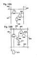
- the pixel shown in Fig. 16A includes a signal line 501, a scanning line 502, a switching TFT 503, a driving TFT 504, a capacitor element 505, a light emitting element 506, and power sources 507 and 508.
- a video signal that has been input to the signal line 501 is input to a gate electrode of the driving TFT 504.
- a gate-source voltage of the driving TFT 504 is determined, and a current flowing between the source and the drain of the driving TFT 504 is determined.
- This current is supplied to the light emitting element 506, and the light emitting element 506 emits light.
- a semiconductor device for driving the light emitting element a polysilicon transistor is used.
- the polysilicon transistor is prone to variation in electrical characteristics, such as a threshold value and an ON current, due to defects in a grain boundary. In the pixel shown in Fig.
- a desired current may be input to the light emitting element, regardless of the characteristics of the TFTs for driving the light emitting element.
- the current input method has been proposed which can control the magnitude of a current that is supplied to a light emitting element regardless of the TFf characteristics.
- the pixel shown in Fig. 16B includes a signal line 601, first to third scanning lines 602 to 604, a current line 605, TFTs 606 to 609, a capacitor element 610, and a light emitting element 611.
- a current source circuit 612 is disposed to each signal line (each column).
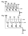
- FIG. 17 Operations of from video signal-writing to light emission will be described by using Fig. 17 .
- reference numerals denoting respective portions conform to those shown in Fig. 16 .
- Figs. 17A to 17C schematically show current paths.
- Fig. 17D shows the relationship between currents flowing through respective paths during a write of a video signal
- Fig. 17E shows a voltage accumulated in the capacitor element 610 also during the write of a video signal, that is, a gate-source voltage of the TFT 608.
- a pulse is input to the first and second scanning lines 602 and 603 to turn the TFTs 606 and 607 ON.
- a signal current flowing through the signal line 601 at this time will be referred to as Idata.
- Idata A signal current flowing through the signal line 601 at this time.
- Fig. 17A since the signal current Idata is flowing through the signal line 601, the current separately flows through current paths I1 and I2 in the pixel.
- a pulse is input to the third scanning line 604, and the TFT 609 is turned ON. Since VGS that has been just written is held in the capacitor element 610, the TFT 608 is already turned ON, and a current equal to Idata flows thereto from the current line 605. Thus, the light emitting element 611 emits light. At this time, when the TFT 608 is set to operate in a saturation region, even if the source-drain voltage of the TFT 608 varies, a light emitting current IEL flowing to the light emitting element 611 flows without variation.
- the current input method refers to a method in which the drain current of the TFT 609 is set to have the same current value as that of the signal current Idata set in the current source circuit 612, and the light emitting element 611 emits light with the luminance corresponding to the drain current.
- a signal current corresponding to a video signal needs to be precisely input to a pixel.
- a signal line driving circuit corresponding to the current source circuit 612 in Fig. 16
- variation in characteristics thereof occurs, thereby also causing variation in characteristics of the signal current.
- the current source circuit 612 shown in Figs. 18A and 18B corresponds to the current source circuit 612 of Fig. 16B .
- the current source circuit 612 includes constant current sources 555 to 558.
- the constant current sources 555 to 558 are controlled by signals that are input via respective terminals 551 to 554.
- the magnitudes of currents supplied from the constant current sources 555 to 558 are different from one another, and the ratio thereof is set to 1 : 2 : 4 : 8.
- Fig. 18B shows a circuit structure of the current source circuit 612, in which the constant current sources 555 to 558 shown therein correspond to transistors.
- the ratio of ON currents of the transistors 555 to 558 is set to 1 : 2 : 4 : 8 according to the ratio (1:2:4:8) of the value of L (gate length)/W (gate width).
- the current source circuit 612 is constituted by polysilicon transistors, and is integrally formed with the pixel portion on the same substrate.
- Non-patent Documents 1 and 2 As described above, conventionally, a signal line driving circuit incorporated with a current source circuit has been proposed (for example, refer to Non-patent Documents 1 and 2).
- digital gradation methods include a method in which a digital gradation method is combined with an area gradation method to represent multi-gradation images (hereinafter, referred to as area gradation method), and a method in which a digital gradation method is combined with a time gradation method to represent multi-gradation images (hereinafter, referred to as time gradation method).
- area gradation method is a method in which one pixel is divided into a plurality of sub-pixels, emission or non-emission is selected in each of the sub-pixels, and the gradation is represented according to a difference between a light emitting area and the other area in a single pixel.
- the time gradation method is a method in which gradation representation is performed by controlling the emission period of a light emitting element. To be more specific, one frame period is divided into a plurality of subframe periods having mutually different lengths, emission or non-emission of a light emitting element is selected in each period, and the gradation is presented according to a difference in length of light emission time in one frame period.
- the digital gradation method the method in which a digital gradation method is combined with a time gradation method (hereinafter, referred to as time gradation method) is proposed. (For example, refer to Patent Document 1).
- JP-A-08 106 075 and JP-A-2000 122 607 relate to displace driving circuits using sample and hold circuits. These circuits can sample and hold a current signal or a voltage signal and can forward the sample voltage to the signal lines.
- the above-mentioned current source circuit 612 sets each on-current of the transistors at 1:2:4:8 by designing each L/W value.
- the transistors 555 to 558 there occurs dispersion in the threshold value or the mobility, by the combined dispersion factors of the gate length, the gate width, and the thickness of the gate insulation film caused by a difference of the manufacturing process and the substrate being used. Therefore, it is difficult to set each on-current of the transistors 555 to 558 accurately at 1:2:4:8. Namely, each current value supplied to the pixel varies depending on each line.
- the present invention is to provide a signal line driving circuit capable of supplying a desired signal current to the pixel while suppressing the influence of the characteristic dispersion of TFTs. Further, the invention is to provide a light emitting device capable of supplying a desired signal current to a light emitting element while suppressing the influence of the characteristic dispersion of TFTs forming both of the pixel and the driving circuit, by using a pixel of a circuit structure in which the influence of the characteristic dispersion of the TFTs is suppressed.
- the invention is to provide a signal line driving circuit of a new structure including an electric circuit (in this specification, referred to as a current source circuit) for flowing a desired constant current in which the influence of the characteristic dispersion of the TFTs is suppresed. Further, the invention is to provide a light emitting device having the above signal line driving circuit.
- a signal current is set in the current source circuit disposed in each signal line, by using the constant current source for video signal.
- the current source circuit with the signal current set has the ability of flowing the current in proportion to the constant current source for video signal. Therefore, the influence of the characteristic dispersion of the TFTs forming the signal line driving circuit can be suppressed by using the current source circuit.
- the constant current source for video signal may be formed integrally with the signal line driving circuit on the substrate.
- the current for video signal the current may be inputted from the outside of the substrate by using the IC and the like.
- a constant current or a current corresponding to the video signal is supplied from the outside of the substrate to the signal line driving circuit.
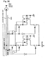
- Fig. 1 The outline of the signal line driving circuit of the invention will be described by using Fig. 1 .
- Fig. 1 the signal line driving circuit in the vicinity of the three signal lines from the i-th line to the (i+2)-th line is shown.
- the current source circuit 420 is disposed in each signal line (each line).
- the current source circuit 420 has the terminal a, the terminal b, and the terminal c.
- the setting signal is entered from the terminal a.
- a current (signal current) is supplied from the constant current source 109 for video signal connected to the current line, to the terminal b.
- the signal held in the current source circuit 420 is output from the terminal c through the switch 101.
- the current source circuit 420 is controlled by the setting signal inputted from the terminal a, the supplied signal current is inputted from the terminal b, and the current in proportion to the signal current is output from the terminal c.
- the switch 101 is disposed between the current source circuit 420 and the pixel connected to the signal line, or between a plurality of current source circuits 420 disposed in mutually different lines, and the on/off operation of the switch 101 is controlled by a latch pulse.
- the operation for finishing writing of the signal current into the current source circuit 420 (the operation for setting the signal current, the operation for setting according to the signal current so as to supply the current in proportion to the signal current, and the operation for setting so that the current source circuit 420 can supply the signal current) is referred to as the setting operation, and the operation for supplying the signal current to the pixel or another current source circuit (the operation of the signal current output by the current source circuit 420) is referred to as the input operation.
- the setting operation the operation for setting operation for setting the signal current so as to supply the current in proportion to the signal current, and the operation for setting so that the current source circuit 420 can supply the signal current
- the input operation the operation for supplying the signal current to the pixel or another current source circuit
- the input operation the operation for supplying the signal current to the pixel or another current source circuit
- the light emitting device includes a panel where the pixel portion having the light emitting elements and the signal line driving circuit are sealed between the substrate and a cover material, a module by mounting IC and the like on the panel, a display, and the like.
- the light emitting device corresponds to a generic name of the panel, module, display, and the like.
- the invention relates to a signal line driving circuit having a first and a second current source circuits corresponding to each of a plurality of signal lines, a shift register, and a constant current source for video signal, which is characterized in that the first current source circuit is disposed in a first latch and the second current source circuit is disposed in a second latch, the first current source circuit includes capacitive means for converting a current supplied from the constant current source for video signal into a voltage, according to a sampling pulse supplied from the shift register, and supplying means for supplying a current corresponding to the converted voltage, and the second current source circuit includes capacitive means for converting a current supplied from the first latch into a voltage, according to a latch pulse, and supplying means for supplying a current corresponding to the converted voltage.
- the invention relates to a signal line driving circuit having a first and a second current source circuits corresponding to each of a plurality of signal lines, a shift register, and n pieces (n is a natural number including 1 and more) of constant current sources for video signal, which is characterized in that the first current source circuit is disposed in a first latch and the second current source circuit is disposed in a second latch, the first current source circuit includes capacitive means for converting a current obtained by adding each current supplied from the n constant current sources for video signal into a voltage, according to a sampling pulse supplied from the shift register, and supplying means for supplying a current corresponding to the converted voltage, the second current source circuit includes capacitive means for converting a current supplied from the first latch into a voltage, according to a latch pulse, and supplying means for supplying a current corresponding to the converted voltage, and the current values supplied from the n constant current sources for video signal are set at 2 ⁇ 0>:2 ⁇ 1>:...:2 ⁇ n>.
- the invention relates to a signal line driving circuit having 2xn pieces of current source circuits corresponding to each of a plurality of signal lines, a shift register, and n pieces (n is a natural number including 1 and more) of constant current sources for video signal, which is characterized in that, of the 2xn current source circuits, the respective n current source circuits are disposed in respective first and second latches, the n current source circuits disposed in the first latch include capacitive means for converting a current supplied from each of the n constant current sources for video signal into a voltage, according to a sampling pulse supplied from the shift register, and supplying means for supplying a current corresponding to the converted voltage, the n current source circuits disposed in the second latch include capacitive means for converting a current obtained by adding each current supplied from the first latch into a voltage, according to a latch pulse, and supplying means for supplying a current corresponding to the converted voltage, a current obtained by adding each current supplied from each of the n current source circuits
- the invention relates to a signal line driving circuit having (n+m) pieces of current source circuits corresponding to each of a plurality of signal lines, a shift register, and n pieces (n is a natural number including 1 and more, n ⁇ m) of constant current sources for video signal, which is characterized in that of the (n+m) current source circuits, the n current source circuits are disposed in a first latch and the m current source circuits are disposed in a second latch, the n current source circuits disposed in the first latch include capacitive means for converting a current supplied from each of the n constant current sources for video signal into a voltage, according to a sampling pulse supplied from the shift register, and supplying means for supplying a current corresponding to the converted voltage, the m current source circuits disposed in the second latch include capacitive means for converting a current obtained by adding each current supplied from each of the n current source circuits disposed in the first latch into a voltage, according to a latch pulse, and supplying means for
- the first and the second latches having each current source circuit are disposed.
- the current source circuit having the supplying means and the capacitive means can supply a current of a predetermined value without having any effect of the characteristic dispersion of the transistors forming the circuit itself.
- the current source circuit disposed in the first latch is controlled according to the sampling pulse supplied from the shift register and the current source circuit disposed in the second latch is controlled according to the latch pulse supplied from the outside. Namely, since the current source circuits disposed in the first and the second latches are controlled by mutually different signals, it is possible to take a long time for the operation of converting the supplied current to a voltage and performs the above operation accurately.
- the signal line driving circuit of the invention can be adopted in both of the analog gradation method and the digital gradation method.
- the TFT can be used in place of a transistor using a general monocrystal, a transistor using SOI, an organic transistor, and the like.
- the invention is to provide a signal line driving circuit having the above current source circuit. Further, the invention is to provide a light emitting device capable of suppressing the influence of the characteristic dispersion of the TFTs forming both of the pixel and the driving circuit and further supplying a desired signal current Idata to the light emitting element, by using the pixel having the circuit structure for suppressing the influence of the characteristic dispersion the of the TFTs.
- a setting signal input from a terminal a represents a sampling pulse or a latch pulse output from a shift register.
- a setting signal input from the terminal a in Fig. 1 corresponds to the sampling pulse or the latch pulse.
- the setting operation of the current source circuit 420 is performed in accordance with the sampling pulse or the latch pulse output from the shift register.
- the signal line driving circuit of the invention has a shift register, a first latch circuit and a second latch circuit.
- the first and the second latch circuits have current source circuits, respectively. That is, as a setting signal, a sampling pulse output from a shift register is input to the terminal a in the current source circuit of the first latch circuit. And, as a setting signal, a latch pulse is input to the terminal a in the current source circuit of the second latch circuit.
- a current (a signal current) from a video data line is supplied to perform the setting operation in the current source circuit of the first latch circuit in concurrence with the sampling pulse output from the shift register. Subsequently, the signal current stored in the first latch circuit is output to the second latch circuit in concurrence with the latch pulse. At this time, in the second latch circuit, the current (a signal current) output from the first latch circuit is supplied to perform the setting operation in the current source circuit of the second latch circuit. Subsequently, the signal current stored in the second latch circuit is output to a pixel via the signal line.
- the current source circuit of the first latch circuit when the current source circuit of the first latch circuit performs the setting operation, at the same time, the current source circuit of the second latch circuit outputs the signal current to the pixel, that is, performs input operation. Then, the current source circuit of the first latch circuit performs input operation in concurrence with the latch pulse, in other words, when the first latch outputs a current to the second latch, at the same time, the current source circuit of the second latch uses the current output from the first latch to perform the setting operation.
- the signal current provided from the video date line has a magnitude depending on the video signal. Therefore, since the current provided to the pixel has a magnitude in proportion to the signal current, it becomes possible to display image (gray scale).
- a shift register has a structure including, for example, flip-flop circuits (FFs) in a plurality of columns.
- a clock signal (S-CLK), a start pulse (S-SP), and an inverted clock signal (S-CLKb) are input to the shift register, and signals serially output according to the timing of the input signals are called sampling pulses.
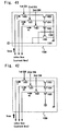
- a circuit including switches 104, 105a, and 116, a transistor 102 (n-channel type), and a capacitor element 103 for holding a gate-source voltage VGS of the transistor 102 corresponds to the current source circuit 420.
- the switch 104 and the switch 105a are turned ON by a signal input via the terminal a.
- a current is supplied to the current source circuit of the first latch circuit via a terminal b from a constant current source for video signal 109 (hereafter referred to as constant current source 109) connected to a current line (video line), and a charge is retained in the capacitor element 103. The charge is retained in the capacitor element 103 until the current supplied from the constant current source 109 becomes identical with a drain current of the transistor 102.
- a current is supplied to the current source circuit of the second latch circuit via the terminal b from the current source circuit of the first latch circuit, and a charge is retained in the capacitor element 103.
- the charge is retained in the capacitor element 103 until the current supplied from the current source circuit of the first latch circuit becomes identical with a drain current of the transistor 102.
- the switch 104 and the switch 105a are turned OFF by a signal input via the terminal a.
- the transistor 102 is imparted with a capability of flowing a current having a magnitude corresponding to that of the signal current Idata. If the switch 101 and the switch 116 are turned into a conductive state, in the current source circuit of the first latch circuit, a current via a terminal c flows to the current source circuit of the second latch circuit. At this time, since the gate voltage of the transistor 102 is maintained at a predetermined gate voltage by the capacitor element 103, a drain current corresponding to the signal current Idata flows through the drain region of the transistor 102.
- a current flows to the pixel connected to the signal line via the terminal c.
- the gate voltage of the transistor 102 is maintained at a predetermined gate voltage in the capacitor element 103, a drain current corresponding to the current (signal current Idata) output from the first latch circuit flows through the drain region of the transistor 102.
- influence of the variation in characteristics of the transistors constituting the signal line driving circuit is suppressed, and the magnitude of the current input to the pixel can be controlled.
- connection structure of the switch 104 and the switch 105a is not limited to the structures shown in Fig. 6A .
- the structure may be such that one side of the switch 104 is connected to the terminal b, and the other side thereof is connected the gate electrode of the transistor 102; and one side of the switch 105a is connected to the terminal b via the switch 104, and the other side thereof is connected to the switch 116. Then, the switch 104 and the switch 105a are controlled by a signal input from the terminal a.
- the switch 104 may be disposed between the terminal b and the gate electrode of the transistor 104, and the switch 105a may be disposed between the terminal b and the switch 116.
- lines, switches, and the like may be disposed such that the connection is structured as shown in Fig. 28(A1) in the setting operation, and the connection is structured as shown in Fig. 28(A2) in the input operation.
- the number of lines, the number of switches, and the structure are not particularly limited.
- the signal setting operation (setting operation) and the signal inputting operation (input operation) to the pixel or the current source circuit that is, the current outputting operation from the current source circuit cannot be performed simultaneously.
- a circuit including a switch 124, a switch 125, a transistor 122 (n-channel type), a capacitor element 123 for retaining a gate-source voltage VGS of the transistor 122, and a transistor 126 (n-channel type) corresponds to the current source circuit 420.
- the transistor 126 functions as either a switch or a part of a current source transistor.
- the switch 124 and the switch 125 are turned ON by a signal input via the terminal a. Then, in the current source circuit of the first latch circuit, a current is supplied via the terminal b from the constant current source 109 connected to the current line, and a charge is retained in the capacitor element 123. The charge is retained therein until the signal current Idata flown from the constant current source 109 becomes identical with a drain current of the transistor 122. Note that, when the switch 124 is turned ON, since a gate-source voltage VGS of the transistor 126 is set to 0 V, the transistor 126 is turned OFF.
- a signal current Idata is supplied via the terminal b from the first latch circuit, and a charge is retained in the capacitor element 123. The charge is retained therein until the current flown from the first latch circuit becomes identical with a drain current of the transistor 122. Note that, when the switch 124 is turned ON, since a gate-source voltage VGS of the transistor 126 is set to 0 V, the transistor 126 is turned OFF.
- the switch 124 and the switch 125 are turned OFF.
- the transistor 122 in the current source circuit of the first latch circuit is imparted with a capability of flowing a current having a magnitude corresponding to that of the signal current Idata.
- the switch 101 signal current control switch
- a current flows to the current source circuit of the second latch circuit via the terminal c.
- the gate voltage of the transistor 122 is maintained by the capacitor element 123 at a predetermined gate voltage, a drain current corresponding to the signal current Idata flows through the drain region of the transistor 122.
- the transistor 122 in the current source circuit of the second latch circuit is imparted with a capability of flowing a current having a magnitude corresponding to that of the current (the signal current Idata) output from the current source circuit of the first latch circuit. If the switch 101 (signal current control switch) is turned into the conductive state, a current flows to a pixel connected to the signal line via the terminal c. At this time, since the gate voltage of the transistor 122 is maintained by the capacitor element 123 at a predetermined gate voltage, a drain current corresponding to the signal current Idata flows through the drain region of the transistor 122.
- the number of switches, the number of lines, and the connections thereamong are not particularly limited. Specifically, referring to Fig. 28B , lines and switches may be disposed such that the connection is structured as shown in Fig. 28(B1) in the setting operation, and the connection is structured as shown in Fig. 28(B2) in the input operation. In particular, in Fig. 28(B2) , it is sufficient that the charge accumulated in a capacitor element 123 does not leak.
- the signal setting operation (setting operation) and the signal inputting operation (input operation) to the pixel or the current source circuit that is, the current outputting operation from the current source circuit cannot be performed simultaneously.
- a circuit including a switch 108, a switch 110, transistors 105b, 106 (n-channel type), and a capacitor element 107 for retaining gate-source voltage VGS of the transistors 150b and 106 corresponds to the current source circuit 420.
- the switch 108 and the switch 110 are turned ON by a signal input via the terminal a. Then, in the current source circuit of the first latch circuit, a current is supplied via the terminal b from the constant current source 109 connected to the current line, and a charge is retained in the capacitor element 107. The charge is retained therein until the signal current Idata flown from the constant current source 109 becomes identical with a drain current of the transistor 105b. At this time, since the gate electrodes of the transistor 105b and of the transistor 106 are connected to each other, the gate voltages of the transistor 105b and the transistor 106 are retained by the capacitor element 107.
- a current is supplied via the terminal b from the current source circuit of the first latch circuit, and a charge is retained in the capacitor element 107.
- the charge is retained therein until the current (the signal current Idata) flown from the current source circuit of the first latch circuit becomes identical with a drain current of the transistor 105b.
- the gate electrodes of the transistor 105b and of the transistor 106 are connected to each other, the gate voltages of the transistor 105b and the transistor 106 are retained by the capacitor element 107.
- the switch 108 and the switch 110 are turned OFF.
- the transistor 106 is imparted with a capability of flowing a current having a magnitude corresponding to that of the signal current Idata. If the switch 101 is turned to the conductive state, a current flows to the current source circuit of the second latch circuit via the terminal c. At this time, since the gate voltage of the transistor 106 is maintained by the capacitor element 107 at a predetermined gate voltage, a drain current corresponding to the current (the signal current Idata) flows through the drain region of the transistor 106.
- the current (the signal current Idata) output from the first latch circuit is retained in the capacitor element 107, the transistor 106 is imparted with a capability of flowing a current having a magnitude corresponding to that of the current (the signal current Idata). If the switch 101 is turned into the conductive state, a current flows to the pixel connected to the signal line via the terminal c. At this time, since the gate voltage of the transistor 106 is maintained by the capacitor element 107 at a predetermined gate voltage, a drain current corresponding to the current (the signal current Idata) flows thourgh the drain region of the transistor 106. Thus, influence of the variation in characteristics of the transistors constituting the signal line driving circuit is suppressed, and magnitude of the current input to the pixel can be controlled.
- characteristics of the transistor 105b and the transistor 106 need to be the same to cause the drain current corresponding to the signal current Idata to flow precisely through the drain region of the transistor 106.
- values such as mobility and thresholds of the transistor 105b and the transistor 106 need to be the same.
- the value of W (gate width)/L (gate length) of each of the transistor 105b and the transistor 106 may be arbitrarily set, and a current proportional to the signal current Idata supplied from the constant current source 109 and the like may be supplied to the pixel.
- the values of W/L of the transistor 105b and the transistor 106, which is connected to the constant current source 109 is set high, whereby the write speed can be increased by supplying a large current from the constant current source 109.
- the signal setting operation (setting operation) can be performed simultaneously with the signal inputting operation (input operation) to the pixel.
- Each of the current source circuits 420 of Figs. 6D and 6E has the same circuit element connection structures as that of the current source circuit 420 of Fig. 6C , except for the connection structure of the switch 110.
- the operation of the current source circuit 420 of each of Figs. 6D and 6E conforms to the operation of the current source circuit 420 of Fig. 6C , a description thereof will be omitted in the present Device form.
- the number of switches, the number of lines, and the structures thereof are not particularly limited. Specifically, referring to Fig. 28C , lines and switches may be disposed such that the connection is structured as shown in Fig. 28(C1) in the setting operation, and the connection is structured as shown in Fig. 28(C2) in the input operation. In particular, in Fig. 28(C2) , it is sufficient that the charge accumulated in the capacitor element 107 does not leak.
- a circuit including switches 195b, 195c, 195d, and 195f, a transistor 195a, and a capacitor element 195e corresponds to the current source circuit.
- the switches 195b, 195c, 195d, and 195f are turned ON by a signal input via the terminal a. Then, a current is supplied via the terminal b from the constant current source 109 connected to the current line. A predetermined charge is retained in the capacitor element 195e until the signal current supplied from the constant current source 109 becomes identical to a drain current of the transistor 195a.
- the switches 195b, 195c, 195d, and 195f are turned OFF by a signal input via the terminal a.
- the transistor 195a is imparted with a capability of flowing a current having a magnitude corresponding to that of the signal current. This is because the gate voltage of the transistor 195a is set by the capacitor element 195a to a predetermined gate voltage, and a drain current corresponding to a current (reference current) flows through the drain region of the transistor 195a. In this state, a current is supplied to the outside via the terminal c. Note that, in the current source circuit shown in Fig.
- the setting operation for setting the current source circuit to have a capability of flowing a signal current cannot be performed simultaneously with the input operation for inputting the signal current to the pixel.
- the terminal c needs to be connected to another line of the other potential.
- the line potential is represented by Va. Va may be a potential sufficient to flow a current flowing from the terminal b as it is, and may be a power supply voltage Vdd as an example.
- the number of switches, the number of lines, and the structures thereof are not particularly limited. Specifically, referring to Figs. 29B and 29C , lines and switches may be disposed such that the connection is structured as shown in either Fig. 29(B1) or 29(C1) in the setting operation, and the connection is structured as shown in either Fig. 29(B2) or 29(C2) in the input operation.
- each of the transistor 102, the transistor 105b, and the transistor 106 can be of p-channel type.
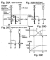
- Fig. 7A shows a circuit structure in which the current-flow direction (direction from the pixel to the signal line driving circuit) is the same, and the transistor 102 shown in Fig. 6A is set to be of p-channel type.
- the transistor 102 shown in Fig. 6A is set to be of p-channel type.
- Fig. 7A with the capacitor element disposed between the gate and the source, even when the source potential varies, the gate-source voltage can be maintained.
- Figs. 7B to 7D show circuit diagrams in which the current-flow directions (directions from the pixel to the signal line driving circuit) are the same, and the transistor 105b and the transistor 106 shown in Figs. 6C to 6E are set to be of p-channel type.
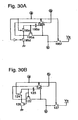
- Fig. 30A shows a case where the transistor 195a is set to be of p-channel type in the structure of Fig. 29 .
- Fig. 30B shows a case where the transistors 122 and 126 are set to be of p-channel type in the structure of Fig. 6B .
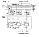
- a circuit including switches 104 and 116, a transistor 102, a capacitor element 103, and the like corresponds to the current source circuit.
- Fig. 32A corresponds to the circuit of Fig. 6A that is partly modified.
- the transistor gate width W varies between the setting operation of the current source and the input operation.
- the connection is structured as shown in Fig. 32B , in which the gate width W is large.
- the connection is structured as shown in Fig. 32C , in which the gate width W is small. Therefore, the value of the current supplied from the terminal b at the time of the setting operation can be made larger than the value of the current supplied from the terminal c at the time of the input operation.
- loads such as wiring resistances and cross capacitances
- Fig. 32 shows the circuit of Fig. 6A that is partly modified.
- the circuit can be easily applied to, for example, other circuits shown in Fig. 6 and to the circuits shown in Fig. 7 , Fig. 29 , Fig. 31 , and Fig. 30 .
- a current flows from the pixel to the signal line driving circuit.
- the current not only flows from the pixel to the signal line driving circuit, but also may flow from the signal line driving circuit to the pixel. It depends on the structure of the pixel circuit that the current flows in a direction from the pixel to the signal line driving circuit or in a direction from the signal line driving circuit to the pixel.
- Vss low potential power source
- Vdd high potential power source
- the transistors 102, 105b, 106, 122, and 126 may be set to be of p-channel type in Fig. 6 .
- Vss may be set to Vdd
- the transistors 102, 105b, and 106 may be of n-channel type.
- lines and switches may be disposed such that the connection is structured as shown in Figs. 31(A1) to 41(D1) in the setting operation, and the connection is structured as shown in Figs. 31(A2) to 41(D2) in the input operation.
- the number of switches, the number of lines and the connection structures thereof are not particularly limited.
- the disposed capacitor element may not be disposed by being substituted by, for example, a gate capacitance of a transistor.
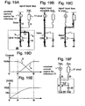
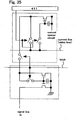
- Figs. 19A to 19C schematically show paths of a current flowing among circuit elements.
- Fig. 19D shows the relationship between the current flowing through each path and the time in writing the signal current Idata to the current source circuit.
- Fig. 19E shows the relationship between the voltage accumulated in a capacitor element 16, that is, the gate-source voltage of a transistor 15, and the time in writing the signal current Idata to the current source circuit.
- numeral 11 denotes a constant current source for video signal
- switches 12 to 14 each are a semiconductor device having a switching function
- numeral 15 denotes a transistor (n-channel type)
- numeral 16 denotes a capacitor element
- numeral 17 denotes a pixel.
- the switch 14, the transistor 15, and the capacitor element 16 form an electric circuit corresponding to a current source circuit 20.
- Drawing lines and reference symbols are shown in Fig. 19A . Since drawing lines and reference symbols shown in Figs. 19B and 19C are similar to those shown in Fig. 19A , they are omitted here.
- a current is supplied form a constant current source 11 for video signal in the current source circuit of the first latch circuit, the current source circuit of the second latch circuit flows a current to the pixel connected to the signal line.
- a current source circuit in which a current is supplied from a constant current source for video signal to a pixel connected to a signal line is described.
- a source region of the n-channel transistor 15 is connected to Vss, and a drain region thereof is connected to the constant current source 11 for video signal.
- One of electrodes of the capacitor element 16 is connected to Vss (the source of the transistor 15), and the other electrode is connected to the switch 14 (the gate of the transistor 15).
- the capacitor element 16 plays a role of holding the gate-source voltage of the transistor 15.
- the pixel 17 is formed of a light emitting element, a transistor, or the like.
- the light emitting element includes an anode, a cathode, and a light emitting layer sandwiched between the anode and the cathode.
- the cathode when used as a pixel electrode, the cathode is referred to as an opposing electrode; in contrast, when the cathode is used as a pixel electrode, the anode is referred to as an opposing electrode.
- the light emitting layer can be formed of a known light emitting material.
- the light emitting layer has two structures: a single layer structure and a laminate structure, and the present invention may use any one of known structures.
- Luminescence in the light emitting layer includes light emission (fluorescence) in returning from a singlet excited state to a normal state and light emission (phosphorescence) in returning from a triplet excited state to a normal state.
- the present invention may be applied to a light emitting device using either one or both of the two types of light emission.
- the light emitting layer is formed of a known material such as an organic material or an inorganic material.
- the current source circuit 20 is provided in the signal line driving circuit.
- a current corresponding to the signal current Idata flows via, for example, a circuit element included in the signal line or the pixel from the current source circuit 20 provided in the signal line driving circuit.
- Fig. 19 is a diagram for briefly explaining the outline of the relationship among the constant current source 11 for video signal, the current source circuit 20, and the pixel 17, a detailed illustration of the structure is omitted.
- Figs. 19A and 19B an operation (setting operation) of the current source circuit 20 for retaining the signal current Idata will be described by using Figs. 19A and 19B .
- the switch 12 and the switch 14 are turned ON, and the switch 13 is turned OFF.
- the signal current Idata is output from the constant current source 11 for video signal, and flows to the current source circuit 20 from the constant current source 11 for video signal.
- the current flows separately through current paths I1 and I2 in the current source circuit 20, as shown in Fig. 19A.
- the potential difference between both the electrodes of the capacitor element 16 serves as the gate-source voltage of the transistor 15.
- charge accumulation in the capacitor element 16 continues until the gate-source voltage of the transistor 15 reaches a desired voltage, that is, a voltage (VGS) that allows the transistor is to be flown with the current Idata.
- VGS voltage
- Idata I2 is established ( Fig. 19B ).
- the operation is divided into an operation (setting operation; corresponding to Figs. 19A and 19B ) for completing a write of the signal current Idata to the current source circuit 20, and an operation (input operation; corresponding to Fig. 19C ) for inputting the signal current Idata to the pixel). Then, in the pixel, a current is supplied to the light emitting element in accordance with the input signal current Idata.
- the current source circuit 20 of Fig. 19 is not capable of performing the setting operation and the input operation simultaneously.
- at least two current source circuits are preferably provided to each of a plurality of signal lines each of which is connected with a plurality of pixels and which are provided in a pixel portion.
- only one current source circuit may be provided for each signal line (each column).
- the transistor 15 of the current source circuit 20 shown in each of Figs. 19A to 19C is of n-channel type
- the transistor 15 of the current source circuit 20 may be of p-channel type, of course.
- a circuit diagram for the case where the transistor 15 is of p-channel type is shown in Fig. 19 .
- numeral 31 denotes a constant current source for video signal
- switches 32 to 34 each are a semiconductor device (transistor) having a switching function
- numeral 35 denotes a transistor (p-channel type)
- numeral 36 denotes a capacitor element
- numeral 37 denotes a pixel.
- the switch 34, the transistor 35, and the capacitor element 36 form an electric circuit corresponding to a current source circuit 24.
- the transistor 35 is of p-channel type. One of a source region and a drain region of the transistor 35 is connected to Vdd, and the other is connected to the constant current source 31. One of electrodes of the capacitor element 36 is connected to Vdd, and the other electrode is connected to the switch 36.
- the capacitor element 36 plays a role of holding the gate-source voltage of the transistor 35.
- the current-flow direction is the same as in Fig. 19F , in which the transistor 35 is of n-channel type.
- the capacitor element 36 is connected between the gate and the source of the transistor 35.
- the source potential of the transistor 35 varies between the setting operation and the input operation. However, even when the source potential varies, since the gate-source voltage is retained, a normal operation is implemented.
- Figs. 20A to 20C schematically show paths through which a current flows among circuit elements.
- Fig. 20D shows the relationship between the current flowing through each path and the time in writing the signal current Idata to the current source circuit.
- Fig. 20E shows the relationship between the voltage accumulated in a capacitor element 46, that is, the gate-source voltages of transistor 43, 44, and the time in writing the signal current Idata to the current source circuit. Further, in the circuit diagrams of Figs.
- numeral 41 denotes a constant current source for video signal
- a switch 42 is a semiconductor device having a switching function
- numerals 43 and 44 denote transistors (n-channel type)
- numeral 46 denotes a capacitor element
- numeral 47 denotes a pixel.
- the switch 42, the transistors 43 and 44, and the capacitor element 46 compose an electric circuit corresponding to a current source circuit 25. Note that drawing lines and reference symbols are shown in Fig. 20A , and since drawing lines and reference symbols shown in Figs. 20B and 20C conform to those shown in Fig. 20A , they are omitted.
- a current is supplied form a constant current source 11 for video signal in the current source circuit of the first latch circuit
- the current source circuit of the second latch circuit flows a current to the pixel connected to the signal line.
- a current source circuit in which a current is supplied from a constant current source for video signal to a pixel connected to a signal line is described.
- a source region of the n-channel transistor 43 is connected to Vss, and a drain region thereof is connected to the video signal current source 41.
- a source region of the n-channel transistor 44 is connected to Vss, and a drain region thereof is connected to a terminal 48 of the light emitting element 47.
- One of electrodes of the capacitor element 46 is connected to Vss (the sources of the transistors 43 and 44), and the other electrode thereof is connected to the gate electrodes of the transistors 43 and 44.
- the capacitor element 46 plays a role of holding gate-source voltages of the transistors 43 and 44.
- the current source circuit 25 is provided in the signal line driving circuit.
- a current corresponding to the signal current Idata flows via, for example, a circuit element included in the signal line or the pixel, from the current source circuit 25 provided in the signal line driving circuit.
- Fig. 20 is a diagram for briefly explaining the outline of the relationship among the constant current source for video signal 41, the current source circuit 25, and the pixel 47, a detailed illustration of the structure is omitted.
- the sizes of the transistors 43 and 44 are important.
- a case where the sizes of the transistors 43 and 44 are identical and a case the sizes are mutually different will be described.
- the case where the sizes of the transistors 43 and 44 are mutually identical will be described by using the signal current Idata.
- the case where the sizes of the transistors 43 and 44 are mutually different will be described by using a signal current Idata1 and a signal current Idata2.
- the sizes of the transistors 43 and 44 are determined using the value of W (gate width)/L (gate length) of each transistor.
- Figs. 20A and 20B operation for retaining the signal current Idata in the current source circuit 20 will be described by using Figs. 20A and 20B .
- the switch 42 when the switch 42 is turned ON, the signal current Idata is set in the video signal current source 41, and flows from the constant current source for video signal 41 to the current source circuit 25.
- the signal current Idata since the signal current Idata is flowing from the constant current source for video signal 41, the current flows separately through current paths I1 and I2 in the current source circuit 20, as shown in Fig. 20A.
- the potential difference between both the electrodes of the capacitor element 46 serves as the gate-source voltage of each of the transistors 43 and 44.
- charge accumulation in the capacitor element 46 continues until the gate-source voltages of the transistors 43 and 44 each reach a desired voltage, that is, a voltage (VGS) that allows the transistor 44 to be flown with the current Idata.
- VGS voltage
- Idata I2 is established ( Fig. 20B ).
- a current can be flown to the pixel 47 by using the current supplied from the video signal current source 41. That is, the setting operation for setting a signal for the current source circuit 20 can be implemented simultaneously with the operation (input operation) for inputting a signal to the pixel.
- the W/L value of the transistor 43 is preferably set larger than the W/L value of the transistor 44. This is because the signal current Idata1 can be increased when the W/L value of the transistor 43 is set large. In this case, when the current source circuit is set with the signal current Idata1, Loads (cross capacitances, wiring resistances) can be charged. Thus, the setting operation can be completed quickly.
- the transistors 43 and 44 of the current source circuit 25 in each of Figs. 20A to 20C are of n-channel type, but the transistors 43 and 44 of the current source circuit 25 may be of p-channel type.
- Fig. 21 shows a circuit diagram in which the transistors 43 and 44 are of p-channel type.
- numeral 41 denotes a constant current source
- a switch 42 is a semiconductor device having a switching function
- numerals 43 and 44 denote transistors (p-channel type)
- numeral 46 denotes a capacitor element
- numeral 47 denotes a pixel.
- the switch 42, the transistors 43 and 44, and the capacitor element 46 form an electric circuit corresponding to a current source circuit 26.
- a source region of the p-channel transistor 43 is connected to Vdd, and a drain region thereof is connected to the constant current source 41.
- a source region of the p-channel transistor 44 is connected to Vdd, and a drain region thereof is connected to a terminal 48 of the light emitting element 47.
- One of electrodes of the capacitor element 46 is connected to (source), and the other electrode is connected to the gate electrodes of the transistors 43 and 44.
- the capacitor element 46 plays a role of holding gate-source voltages of the transistors 43 and 44.
- the current having the same magnitude as that of the signal current Idata set in the current source flows to the pixel.
- the signal current Idata set in the constant current source is identical in value with the current flowing to the pixel.
- the current is not influenced by variation in characteristics of the transistors provided in the current source circuit.
- the signal current Idata cannot be output to the pixel from the current source circuit in a period during which the setting operation is performed.
- two current source circuits are preferably provided for each signal line, in which an operation (setting operation) for setting a signal is performed to one of the current source circuits, and an operation (input operation) for inputting Idata to the pixel is performed using the other current source circuit.
- the current source circuit of each of Figs. 29A and 30A is similar to the current source circuit of Fig. 19 , except for the connection and current-flow paths.
- the current source circuit of Fig. 32A is similar, except for the difference in magnitude between the current supplied from the constant current source and the current flowing from the current source circuit.
- the current source circuits of Figs. 6B and 30B are similar, except for the difference in magnitude between the current supplied from the constant current source and the current flowing from the current source circuit.
- Fig. 32A only the gate width W of the transistor is different between the setting operation and the input operation; in Figs. 6B and 30B , only the gate length L is different between the setting operation and the input operation; and others are similar to those of the structure of the current source circuit in Fig. 19 .
- the signal current Idata set in the constant current source and the value of the current flowing to the pixel are dependent on the sizes of the two transistors provided in the current source circuit.
- the signal current Idata set in the constant current source and the current flowing to the pixel can be arbitrarily changed by arbitrarily designing the sizes (W (gate width)/L (gate length)) of the two transistors provided in the current source circuit.
- output of precise signal current Idata to the pixel is difficult in the case where variation is caused in the characteristics of the two transistors, such as threshold values and mobility.
- the signal can be input to the pixel during the setting operation. That is, the setting operation for setting the signal can be performed simultaneously with the operation (input operation) for inputting the signal to the pixel.
- the current source circuit of Fig. 19 two current source circuits do not need to be provided in a single signal line.
- the present invention with the above structure can suppress the influence of variation in the TFT characteristics and supply a desired current to the outside.
- the light emitting device of the invention comprises a pixel portion 402 with a plurality of pixels arranged in a matrix shape, on a substrate 401, and a signal line driving circuit 403, a first scanning line driving circuit 404, and a second scanning line driving circuit 405 arranged around the pixel portion 402.
- a signal line driving circuit 403 although it has the signal line driving circuit 403 and two sets of scanning line driving circuits 404 and 405, the invention is not restricted to this.
- the number of the driving circuits can be determined depending on the structure of the pixels.
- a signal is supplied from the outside to the signal line driving circuit 403, the first scanning line driving circuit 404, and the second scanning line driving circuit 405, through the FPC 406.
- Each of the first scanning line driving circuit 404 and the second scanning line driving circuit 405 has a shift register 407 and a buffer 408.
- the shift register 407 supplies sampling pulses sequentially, according to a clock signal (G-CLK), a start pulse (S-SP), and a clock inverse signal (G-CLKb). Thereafter, the sampling pulses amplified by the buffer 408 are supplied to the scanning lines to make each one line into a selection state. Then, a signal current Idata is sequentially written into the controlled pixel from the signal line, according to the selected scanning line.
- a level shifter circuit may be arranged between the shift register 407 and the buffer 408, a level shifter circuit may be arranged.
- the voltage amplitude can be increased by placing the level shifter circuit.
- the structure of the signal line driving circuit 403 will be described below.
- the form of this Device may be freely combined with the Device form 1.
- Fig. 3A shows a schematic view of the signal line driving circuit 403 in the case of performing the analog gradation display or the digital gradation display of one bit.
- the signal line driving circuit 403 has a shift register 415, a first latch circuit 416, and a second latch circuit 417.
- the shift register 415 is formed by a plurality of lines of flip-flop circuits (FF) and the like, to which the clock signal (S-CLK), the start pulse (S-SP), and the clock inverse signal (S-CLKb) are supplied. According to the timing of these signals, sampling pulses are sequentially supplied therefrom.
- FF flip-flop circuits
- sampling pulses supplied from the shift register 415 are supplied to a first latch circuit 416.
- a video signal (digital video signals or analog video signals) is entered in the first latch circuit 416, and the video signal is kept in each line according to the timing of entering the sampling pulses.
- the first latch circuit 416 when the video signal has been kept in every line including the final line, a latch pulse is entered into a second latch circuit 417 in the horizontal retrace time, and the video signal kept in the first latch circuit 416 is all transferred to the second latch circuit 417. Then, it is found that the video signal kept in the second latch circuit 417 has been supplied at once for every one line to each pixel connected to each signal line.
- the sampling pulses are supplied from the shift register 411 again. Thereafter, the operation will be repeated, thereby performing the processing of the video signal for one frame.
- the signal line driving circuit of the invention includes the first latch circuit 416 and the second latch circuit 417 having each current source circuit.
- Fig. 4 shows the outline of the signal line driving circuit 403 in the vicinity of the three signal lines from the i-th line to the (i+2)-th line.
- the signal line driving circuit 403 includes a current source circuit 431, a switch 432, a current source circuit 433, and a switch 434 in each line.
- the switch 432 and the switch 434 are controlled by the latch pulse.
- the mutually inverted signals are entered respectively into the switch 432 and the switch 434. Therefore, the current source circuit 433 performs one of the setting operation and the input operation.
- the current source circuit 431 and the current source circuit 433 are controlled by a signal entered through a terminal a.
- a current (signal current Idata) set by using a constant current source 109 for video signal connected to a video line (current line) through a terminal b is held in the current source circuit 431 belonging to the first latch circuit 416.
- the switch 432 is provided between the current source circuit 431 and the current source circuit 433, and the on/off operation of the switch 432 is controlled by the latch pulse.
- a current supplied from the current source circuit 431 (the first latch circuit 416) is held in the current source circuit 433 belonging to the second latch circuit 417.
- the switch 434 is provided between the current source circuit 433 and the pixel connected to the signal line and the on/off operation of the switch 434 is controlled by the latch pulse.
- the switch 434 provided between the current source circuit 433 and the pixel connected to the signal line can be omitted when a switch is set in the current source circuit 433.
- the switch 434 is not required between the current source circuit 433 and the pixel connected to the signal line.
- the switch 432 provided between the current source circuit 431 and the current source circuit 433 can be also omitted in some cases.
- the signal current Idata is supplied from the current source circuit 433 to the pixel when the video signal is a bright signal.
- the current source circuit 433 doesn't have an ability of supplying a current, no current flows to the pixel.
- the signal current Idata is supplied from the current source circuit 433 to the pixel, according to the video signal. Namely, in the current source circuit 433, the ability (VGS) of supplying a current is controlled by the video signal and the brightness is controlled, according to the amount of the current supplied to the pixels.
- a setting signal supplied from the terminal a means the sampling pulse or the latch pulse supplied from the shift register.
- the setting signal in Fig. 1 corresponds to the sampling pulse or the latch pulse supplied from the shift register.
- the current source circuit is set, according to the sampling pulse or the latch pulse supplied from the shift register.
- the sampling pulse supplied from the shift register 415 is entered into the terminal a of the current source circuit 431 belonging to the first latch circuit 416.
- the latch pulse is entered into the terminal a of the current source circuit 433 belonging to the second latch circuit 417.
- the circuitry of the current source circuit as shown in Fig. 6 , Fig. 7 , Fig. 29 , Fig. 30 , and Fig. 32 , etc. can be freely used in the current source circuit 431 and the current source circuit 433.
- the respective current source circuits may adopt not only one method but also a plurality of methods.
- the setting operation is performed on the first latch circuit for every one line by the constant current source 109 for video signal in Fig. 4 , it is not restricted to this. As illustrated in Fig. 34 , the setting operation can be performed at once in a plurality of lines and in other words, in a multiphasic way. Although two constant current sources 109 for video signal are arranged in Fig. 34 , the setting operation may be performed on the two constant current sources 109 for video signal by another constant current source for video signal separately arranged.
- the current source circuit of the current mirror circuit as shown in Fig. 6C has at least two transistors and the gate electrodes of the two transistors are commonly or electrically connected, as mentioned above.
- the two transistors one of the source region and the drain region of one transistor and one of the source region and the drain region of the other transistor are respectively connected to different circuit elements.
- the current source circuit shown in Fig. 20 of the two transistors, one transistor (one of the source region and the drain region of it) is connected to the constant current source and the other transistor (one of the source region and the drain region of it) is connected to the pixel.
- the current source circuit 431 belonging to the first latch circuit 416 is the circuit as shown in Fig. 6A and the current source circuit 433 belonging to the second latch circuit 417 is the current mirror circuit as shown in Fig. 6C .
- the two transistors belonging to the current source circuit 433 that is the current mirror circuit as shown in Fig. 6C one is connected to the current source circuit 431 belonging to the first latch circuit 416 and the other is connected to the pixel through the switch 434.
- the switch 434 is not necessarily required. This is why the current supplied from the current source circuit 431 belonging to the first latch circuit 416 never flows to the pixel and the setting operation and the input operation can be performed at once in the case where the current source circuit 433 belonging to the second latch circuit 417 is the current mirror circuit as shown in Fig. 6C .
- the transistor for performing the setting operation and the transistor for performing the input operation are different.
- the current flowing between the source/drain of the transistor for performing the setting operation never flows into between the source/drain of the transistor for performing the input operation. Further, it is true in the other way around. Therefore, the current supplied from the current source circuit 431 belonging to the first latch circuit 416 flows into the transistor for performing the setting operation, but does not flow into the transistor for performing the input operation, and the current does not flow to the pixel. Accordingly, without setting of the switch 434, the setting operation and the input operation are not badly affected with each other, thereby causing no problem.
- the current of (2xP) will be supplied from the constant current source 109 for video signal.
- the W/L ratio of the transistor at a proper value, the current supplied from the constant current source 109 for video signal can be increased, thereby performing the setting operation of the current source circuit 431 quickly and accurately.
- circuit diagram in this case is shown in Fig. 35 .
- the current source circuit 431 belonging to the first latch circuit 416 is the current mirror circuit as shown in Fig. 6C and the current source circuit 433 belonging to the second latch circuit 417 is the circuit as shown in Fig. 6A .
- the two transistors of the current source circuit 431 that is the current mirror circuit as shown in Fig. 6C one is connected to the constant current source 109 for video signal and the other is connected to the current source circuit 433 belonging to the second latch circuit 417.
- the current amount given to the pixel is P.
- the W/L ratio of the transistor connected to the current source circuit 433 belonging to the second latch circuit 417 is Wa and that the W/L ratio of the transistor connected to the constant current source 109 for video signal is (2xWa)
- the current of (2xP) will be supplied from the constant current source 109 for video signal.
- the W/L ratio of the transistor at a proper value, the current amount supplied form the constant current source 109 for video signal can be increased, thereby performing the setting operation of the current source circuit 431 quickly and accurately.
- circuit diagram in this case is shown in Fig. 36 .
- the current amount given to the pixel is P.
- the W/L ratio of the transistor connected to the pixel is Wa
- the W/L ratio of the transistor connected to the current source circuit belonging to the first latch circuit 416 is (2xWa). Then, the current amount becomes twice in the current source circuit 433 belonging to the second latch circuit 417.
- the circuit diagram in this case is shown in Fig. 37 .
- the switch 432 does not have to be provided between the current source circuit belonging to the first latch circuit and the current source circuit belonging to the second latch circuit. In this case, however, the current continues flowing between the current source circuit belonging to the first latch circuit and the current source circuit belonging to the second latch circuit, which is not preferable.
- circuit diagram in this case is shown in Fig. 39 .
- the current source circuits of only one structure are not used but a combination of the current source circuits of various structures may be also used, such as using the circuit as shown in Fig. 6A or the current mirror circuit as shown in Fig. 6C .
- the current source circuits of various structures may be mixed, also in those belonging to the second latch circuit 417.
- the above may be summarized as follows: by adopting the current mirror circuit as shown in Fig. 6C as the current source circuits (the current source circuit 431 and the current source circuit 433) and further setting the W/L ratio at a proper value, the current supplied from the constant current source 109 for video signal can be increased. As a result, the setting operation of the current source circuits (the current source circuit 431 and the current source circuit 433) can be performed accurately.
- the current mirror circuit as shown in Fig. 6C , however, there are at least two transistors having the gate electrodes in common, and if the characteristics of the two transistors are dispersed, the currents supplied therefrom are dispersed.
- the current amount can be changed.
- the current is increased at the setting operation time. As a result, the setting operation can be performed quickly.
- the current at the setting operation time corresponds to the current supplied from the constant current source 109 for video signal in the case of the current source circuit of the first latch circuit, and it corresponds to the current supplied form the current source of the first latch circuit in the case of the current source circuit of the second latch circuit.
- the current flowing at the setting operation time is substantially equal to the current flowing at the input operation time. Therefore, the current for performing the setting operation cannot be increased.
- the transistor of supplying the current at the setting operation time and the transistor of supplying the current at the input operation time are the same. Accordingly, there is no ill effect caused by the dispersion between the transistors. Therefore, it is preferable to use the current source circuits in a proper combination, for example, using the current mirror circuit as shown in Fig. 6C in the portion where a large amount of the current is desired at the setting operation time and using the circuit as shown in Fig. 6A in the portion where the more accurate output of the current is desired.
- the current mirror circuit as shown in Fig. 6C there are at least two transistors having the gate electrodes in common, and if the characteristics of the two transistors are dispersed, the current supplied therefrom are dispersed. However, if the characteristics of the two transistors are uniform, the currents supplied therefrom will not be dispersed. Conversely, in order not to disperse the output currents, it is necessary to make the characteristics of the two transistors uniform. Namely, it is necessary to make the characteristics uniform between the two transistors having the gate electrodes in common, in the current mirror circuit as shown in Fig. 6C . It is not necessary to make the characteristics uniform between the transistors having no common gate electrode. This is because the setting operation is performed on the respective current source circuits.
- the transistor that becomes the object of the setting operation and the transistor used at the input operation time need to have the same characteristics.
- the characteristics are not uniform between the transistors having no common gate electrode, since the respective current source circuits are set according to the setting operation, the characteristic dispersion can be corrected.
- any polarity inductivity type will do.
- the layout view about the current source circuit disposed in the first latch is shown in Fig. 45 and the corresponding circuit view is shown in Fig. 46 .
- This Device form can be freely combined with any of the Device forms 1 and 2.
- Fig. 3B shows the schematic view of the signal line driving circuit 403 in the case of performing the digital gradation display of two bits.
- the signal line driving circuit 403 has the shift register 415; the first latch circuit 416, and the second latch circuit 417.
- the shift register 415 is formed by a plurality of lines of the flip-flop circuits (FF) and the like, where the clock signal (S-CLK), the start pulse (S-SP), and the clock inverse signal (S-CLKb) are entered. According to the timing of these signals, the sampling pulses are sequentially supplied therefrom.
- the sampling pulses supplied from the shift register 415 are entered to the first latch circuit 416.
- a video signal Digital Data 1, Digital Data 2 is being entered and according to the timing of entering the sampling pulses, the video signal is kept in each line.
- the latch pulse is entered into the second latch circuit 417 in the horizontal retrace time, and the video signal held in the first latch circuit 416 is all transferred to the second latch circuit 417. Then, it is found that one line of the video signal kept in the second latch circuit 417 has been supplied at once to the pixel connected to the signal line.
- the digital video signal of one bit is entered from a current line connected to the constant current source 109 for video signal of one bit.
- the digital video signal of two bits is entered from a current line connected to the constant current source 109 for video signal of two bits.
- the signal currents (corresponding to the video signal) set by the constant current sources 109 for one-bit video signal and two-bit video signal are held in the current source circuits.
- the structure of the first latch circuit 415 and the second latch circuit 416 will be described by using Figs. 5 , 26 and 27 .
- Fig. 5 shows the outline of the signal line driving circuit 403 in the vicinity of the three signal lines from the i-th line to the (i+2)-th line.
- the constant current source 109 for one-bit video signal and the constant current source 109 for two-bit video signal are connected to the current source circuit 431 belonging to the first latch circuit 416.
- the current of the total sum of the current of the one-bit video signal and the current of the two-bit video signal flows in the current source circuit 431 belonging to the first latch circuit 416.
- Fig. 26 shows the outline of the signal line driving circuit 403 in the vicinity of the three signal lines from the i-th line to the (i+2)-th line.
- the signal line driving circuit 403 includes the current source circuit 431a and the switch 432a, the current source circuit 433a and the switch 434a, the current source circuit 431b and the switch 432b, and the current source circuit 433b and the switch 434b in each line.
- the switches 432a, 434a, 432b, and 434b are controlled according to the latch pulse.
- the switch 434 provided between the current source circuit 433 and the pixel connected to the signal line can be omitted. Or, the switch 434 provided between the current source circuit 433 and the pixel connected to the signal line is not necessary. Similarly to the switch 434 provided between the current source circuit 433 and the pixel connected to the signal line, the switch 432 provided between the current source circuit 431 and the current source circuit 433 also can be omitted.
- Each of the current source circuits 431a, 433a, 431b, and 433b has the terminal a, the terminal b, and the terminal c.
- Each of the current source circuits 431a, 433a, 431b, and 433b are controlled by a signal supplied through the terminal a.
- the current (signal current Idata) set by using the constant current source 109 for video signal connected to the video line (current line) through the terminal b is held in the current source circuit 431a and the current source circuit 431b.
- the current (signal current Idata) supplied from the current source circuit 431a and the current source circuit 431b belonging to the first latch circuit 416 through the terminal b is held in the current source circuit 433a and the current source circuit 433b.
- the current set in the constant current source 109 for one bit is held in the current source circuit 431a and the current source circuit 433a.
- the current set in the current generator 109 for two bits is held in the current source circuit 431b or the current source circuit 433b.
- the respective switches 434a and 434b are provided between the pixels and the respective current source circuits 433a and 433b, and the on/off operation of the switches 434a and 434b is controlled by the latch pulse.
- the total sum of the current of the one-bit video signal flowing from the current source circuit 433a and the current of the two-bit video signal flowing from the current source circuit 433b flows into the pixel.
- the currents of the respective-bit video signals are added in a portion where the current flows from the current source circuit 433a and the current source circuit 433b toward the pixel, and the D/A conversion is performed. Accordingly, when the current is supplied from the current source circuit to the pixel, the current amount has to be the current value corresponding to the respective bits.
- Fig. 27 shows the outline of the signal line driving circuit 403 in the vicinity of the three signal lines from the i-th line to the (i+2)-th line.
- the signal line driving circuit 403 shown in Fig. 27 is the same as the signal line driving circuit 403 shown in Fig. 26 , except that the current source circuit 433b and the switch 434b are removed and that the current held in the current source circuit 431b is supplied not to the current source circuit 433b but to the current source circuit 433a, and the description thereof is omitted. Since the signal line driving circuit 403 shown in Fig. 27 can lessen the number of the circuit elements compared with the signal line driving circuit 403 shown in Fig. 26 , the occupied area of the signal line driving circuit 403 can be reduced.
- the currents of the respective-bit video signals are added in a portion where the current flows from the current source circuit 431a and the current source circuit 431b toward the current source circuit 433a, and the D/A conversion is performed. Accordingly, when the current is supplied from the pixel to the current source circuit, the current amount has to be the current value corresponding to the respective bits.
- the signal line driving circuit 403 shown in Figs. 5 , 26 , and 27 when the digital video signal is a bright signal, the signal current is supplied from the respective current source circuits to the pixel. On the contrary, when the video signal is a dark signal, the latch pulse between the respective current source circuits and the pixel is controlled, so as not to supply the current to the pixel. Namely, in the respective current source circuits 433a and 433b, the ability of running a constant current (VGS) is controlled by the video signal and brightness is controlled by using the amount of the current to be supplied to the pixel.
- VGS constant current
- sampling pulse supplied from the shift register 415 is entered into the terminal a of the current source circuit belonging to the first latch circuit 416.
- latch pulse is entered into the terminal a of the current source circuit belonging to the second latch circuit 417.
- the current source circuit 433b is not provided in the structure of Fig. 27 .
- the respective current source circuits 431a, 433a, 431b, and 433b can be formed freely by using the circuit structures of the current source circuits shown in Fig. 6 , Fig. 7 , Fig. 29 , Fig. 30 , Fig. 32 , and the like. All the current source circuits 420 can adopt not only one method but also they may adopt a plurality of methods.
- Fig. 26 as the example of the combination of the methods used in the current source circuits (the current source circuits 431a, 431b; 433a, and 433b), in the current source circuit (the current source circuits 431a and 431b) belonging to the first latch circuit 416 and the current source circuits (the current source circuits 433a and 433b) belonging to the second latch circuit 417, the case where one is the circuit as shown in Fig. 6A and the other is the current mirror circuit shown in Fig. 6C will be described.
- the current source circuit of the current mirror circuit as shown in Fig. 6C has at least two transistors and the gate electrodes of the two transistors are common or electrically connected as mentioned above. Of the two transistors, one of the source region and the drain region of one transistor and one of the source region and the drain region of the other transistor are respectively connected to different circuit elements. For example, in the current source circuit shown in Fig. 20 , of the two transistors, one transistor (one of the source region and the drain region of it) is connected to the constant current source and the other transistor (one of the source region and the drain region of it) is connected to the pixel.
- the current source circuits (the current source circuits 431a and 431b) belonging to the first latch circuit 416 are the circuits as shown in Fig. 6A and the current source circuits (the current source circuits 433a and 433b) belonging to the second latch circuit 417 are the current mirror circuits as shown in Fig. 6C .
- the two transistors belonging to the respective current source circuits (the current source circuits 433a and 433b) that are the current mirror circuits as shown Fig. 6C one is respectively connected to the current source circuits 431a and 431b belonging to the first latch circuit 416 and the other is respectively connected to the pixel through the switches 434a and 434b.
- the current supplied from the constant current source 109 for video signal can be increased, thereby performing the setting operation of each current source circuit (the current source circuits 431a and 431b) quickly and accurately.
- the W(gate width)/L(gate length) ratio of each transistor may be changed depending on each bit.
- the current flowing from the constant current source 109 for video signal of the lower bit and the current flowing from the first latch circuit to the second latch circuit can be increased. Namely, the current flowing at the setting operation time can be increased.
- the current source circuits (the current source circuits 433a and 433b) belonging to the second latch circuit 417 are the current mirror circuits as shown in Fig. 6C , the magnification of a current varies in the above current mirror currents.
- the current amount becomes smaller. Namely, the current is decreased at an input operation time and the current flowing to the pixel becomes smaller. Therefore, in the case of supplying the current from the first latch circuit to the second latch circuit and performing the setting operation on the current source circuits of the second latch circuit, the current flowing to the current source circuits of the second latch circuit does not become smaller but it is large, and therefore, the setting operation can be performed quickly.
- the current source circuits (the current source circuits 431a and 431b) belonging to the first latch circuit 416 are the current mirror circuit as shown in Fig. 6C and the current source circuits (the current source circuits 433a and 433b) belonging to the second latch circuit 417 are the circuits as shown in Fig. 6A .
- the current source circuits 433a and 433b belonging to the current mirror circuit as shown in Fig. 6C
- the current source circuits 433a and 433b belonging to the current mirror circuit as shown in Fig. 6C
- one is connected to the constant current source 109 for video signal (for one bit and two bits) and the other is connected to each current source circuit (the current source circuits 433a and 433b) belonging to the second latch circuit 417.
- the current supplied from the constant current source 109 for video signal can be increased, thereby performing the setting operation of the current source circuits (the current source circuits 431a and 431b) quickly and accurately.
- the current source circuits (the current source circuits 431a and 431b) belonging to the first latch circuit 416 are the current mirror circuits as shown in Fig. 6C , the W(gate width)/L(gate length) ratio of each transistor may be changed depending on each bit. As a result, the current flowing from the constant current source 109 for video signal of the lower bit can be much more increased.
- the W/L ratio of the transistor connected to the constant current source 109 for video signal is set larger than the W/L ratio of the transistor connected to the second latch circuit.
- the W/L ratio of the transistor of performing the setting operation is set larger than the W/L ratio of the transistor of performing the input operation. Then, the current for performing the setting operation, in other words, the current flowing from the constant current source 109 for video signal can be much more increased.
- the current amount given to the pixel is P.
- the W/L ratio of the transistor connected to the pixel is Wa
- the W/L ratio of the transistor connected to each current source circuit belonging to the first latch circuit 416 is (2xWa). Then, the current amount becomes twice in the second latch circuit 417.
- the W/L ratio of the transistor connected to the constant current source 109 for video signal is (2xWb)
- the W/L ratio of the transistor connected to the second latch circuit 417 becomes Wb.
- the current amount becomes twice in the first latch circuit 416.
- the current of (4xP) will be supplied from the constant current source 109 for video signal (for one bit and two bits).
- the current supplied from the constant current source 109 for video signal can be increased, thereby performing the setting operation of the current source circuit quickly and accurately.
- the current source circuit is the current mirror circuit as shown in Fig. 6C , the W(gate width)/L(gate length) ratio of each transistor may be changed depending on each bit. As a result, the current flowing from the constant current source 109 for video signal of the lower bit can be much more increased.
- the W/L ratio of the transistor of performing the setting operation is made larger than the W/L ratio of the transistor of performing the input operation. Then, the current for performing the setting operation, in other words, the current flowing from the constant current source 109 for video signal can be much more increased.
- the W/L ratio of the transistor connected to the constant current source 109 for video signal is set larger than the W/L ratio of the transistor connected to the second latch circuit.
- the W/L ratio of the transistor connected to the first latch circuit is set larger than the W/L ratio of the transistor connected to the pixel or the signal line.
- the type of the circuit as shown in Fig. 6A may be used or the type of the current mirror circuit as shown in Fig. 6C may be used, in a mixed way.
- the above types may be used in a mixed way.
- the setting operation takes a long time. Then, if the current value is increased by using the current mirror circuit as shown in Fig. 6C , the time taken for the setting operation can be shortened.
- the current mirror circuit as shown in Fig. 6C there are at least two transistors having the gate electrodes in common or electrically connected, and if the characteristics of the two transistors are dispersed, the currents supplied therefrom are dispersed.
- the current value supplied to the pixel or the signal line is small. Therefore, even if the characteristics of the two transistors are dispersed, its influence is a little. Owing to this, in the current source circuit for lower bit, it is effective to use the current mirror circuit as shown in Fig. 6C .
- the current supplied from the constant current source 109 for video signal can be increased.
- the setting operation of the current source circuit can be performed accurately.
- the current mirror circuit as shown in Fig. 6C , there are at least two transistors having the gate electrodes in common, and if the characteristics of the two transistors are dispersed, the currents supplied therefrom are dispersed.
- the current amount can be changed.
- the current at the setting operation time is made larger. As a result, the setting operation can be performed quickly.
- the current at the setting operation time corresponds to the current supplied from the constant current source 109 for video signal in the case of the current source circuit of the first latch circuit, and it corresponds to the current supplied from the current source of the first latch circuit in the case of the current source circuit of the second latch circuit.
- the current flowing at the setting operation time is substantially equal to the current flowing at the input operation time. Therefore, the current for performing the setting operation cannot be increased.
- the transistor for supplying the current at the setting operation time is the same as the transistor for supplying the current at the input operation time. Accordingly, there is no influence of dispersion among the transistors. Therefore, it is preferable to use the circuits in a proper combination, in the respective latch circuits, or in the respective bit-circuits, such as to use the current mirror circuit as shown in Fig. 6C in the portion where a larger current at the setting operation time is desired, and use the circuit as shown in Fig. 6A in the portion where the more accurate current is desired.
- the W(gate width)/L(gate length) ratio of the transistor connected to the current source circuit (the current source circuit 433a) belonging to the second latch circuit 417 is set smaller than that of the transistor connected to the constant current source 109 for video signal, the current amount supplied from the constant current source 109 for video signal can be increased.
- the current amount given to the pixel is P.
- the W/L ratio of the transistor connected to the current source circuit (the current source circuit 433a) belonging to the second latch circuit 417 is Wa
- the W/L ratio of the transistor connected to the constant current source 109 for video signal is (2xWa)
- the current of (2xP) will be supplied from the constant current source 109 for video signal.
- the current amount supplied form the constant current source 109 for video signal can be increased, thereby performing the setting operation of the current source circuits (the current source circuits 431a and 431b) accurately.
- the current source circuits (the current source circuit 431a and 431b) belonging to the first latch circuit 416 are the current mirror circuits as shown in Fig. 6C , the W(gate width)/L(gate length) ratio of each transistor may be changed depending on each bit. As a result, the current flowing from the constant current source 109 for video signal of the lower bit can be much more increased.
- the W/L of the transistor connected to the constant current source 109 for video signal is made larger than the W/L of the transistor connected to the second latch circuit.
- the W/L of the transistor of performing the setting operation is set larger than the W/L ratio of the transistor of performing the input operation. Then, the current for performing the setting operation, in other words, the current flowing from the constant current source 109 for video signal can be much more increased.
- the current source circuits (the current source circuits 431a and 431b) belonging to the first latch circuit 416 are the circuits as shown in Fig. 6A and the current source circuit (the current source circuit 433a) belonging to the second latch circuit 417 is the current mirror circuit as shown in Fig. 6C .
- the two transistors of each current source circuit (the current source circuits 433a and 433b) that is the current mirror circuit as shown Fig. 6C one is connected to the current source circuit (the current source circuit 433a) belonging to the first latch circuit 416 and the other is connected to the pixel.
- the W(gate width)/L(gate length) ratio of the transistor connected to the pixel is set smaller than that of the transistor connected to the current source circuit belonging to the first latch circuit 416, the current amount supplied from the constant current source 109 for video signal or the first latch circuit can be made larger.
- the current supplied from the first latch circuit can be increased, thereby performing the setting operation of each current source circuit (the current source circuits 431a and 431b) accurately.
- the current amount given to the pixel is P.
- the W/L ratio of the transistor connected to the pixel is Wa
- the W/L ratio of the transistor connected to each current source circuit belonging to the first latch circuit 416 is (2xWa). Then, the current amount becomes twice in the second latch circuit 417.
- the W/L ratio of the transistor connected to the constant current source 109 for video signal is (2xWb)
- the W/L ratio of the transistor connected to the second latch circuit 417 becomes Wb.
- the current amount becomes twice in the first latch circuit 416.
- the current of (4xP) will be supplied from the constant current source 109 for video signal (for one bit and two bits).
- the current supplied from the constant current source 109 for video signal can be increased, thereby performing the setting operation of the current source circuit quickly and accurately.
- the current source circuits (the current source circuits 431a and 431b) belonging to the first latch circuit 416 are the current mirror circuits as shown in Fig. 6C , the W(gate width)/L(gate length) ratio of each transistor may be changed depending on each bit. As a result, the current flowing from the constant current source 109 for video signal of the lower bit can be much more increased.
- the W/L ratio of the transistor connected to the constant current source 109 for video signal is made larger than the W/L ratio of the transistor connected to the second latch circuit.
- the W/L ratio of performing the setting operation is made larger than the W/L ratio of the transistor of performing the input operation. Then, the current for performing the setting operation, in other words, the current flowing from the constant current source 109 for video signal can be much more increased.
- the constant current source 109 for one-bit video signal is connected to a video line (Video data line) and the constant current source 109 for two-bit video signal is connected to a video line (Video data line) for two bits.
- the current supplied from the constant current source 109 for one-bit video signal is I
- the current supplied from the constant current source 109 for two-bit video signal is 2I.
- the invention is not restricted to this, but the current amounts respectively supplied from the constant current source 109 for one-bit video signal and the constant current source 109 for two-bit video signal can be the same.
- the operation condition and the load can be the same and further the time of writing signals into the respective current source circuits can be the same.
- the current mirror circuit as shown in Fig. 6C is adopted to the current source circuits (the current source circuits 431a and 431b) belonging to the first latch circuit 416. Further, it is necessary to set the W/L ratio of the transistor belonging to the current source circuit 431a and the transistor belonging to the current source circuit 431b at 2:1. Then, the ratio of the current amount supplied from the current source circuit 431a and the current amount supplied from the current source circuit 431b can be set at 2:1.
- the current mirror circuit as shown in Fig. 6C is adopted to not only the current source circuits for all bits but also the current source circuits for some bit. It is preferable that the current mirror circuit as shown in Fig. 6C is used for the current source circuit for lower bit and the circuit as shown in Fig. 6A is used for the current source circuit for upper bit.
- the current source circuit for upper bit has a great effect on the current value even if the characteristics of the transistors of the current source circuit are a little dispersed. This is why the absolute value of a difference of the currents caused by dispersion is also great, as for the current supplied from the current source circuit for upper bit, since the current value itself is great, even if the characteristics of the transistors are dispersed to the same degree. For example, assume that the characteristics of the transistors are dispersed by 10%. Assuming that the current amount for one bit is I, the dispersion amount is 0.1I. Since the current amount for three bits becomes 8I, the dispersion amount becomes 0.8I. Thus, the current source circuit for upper bit is much influenced even by a little dispersion of the characteristic of the transistor.
- a method of having the least effect from the dispersion is preferable. Further, since the current value in the current for upper bit is great, it is easy to do the setting operation. While, since the current value itself is small in the current for lower bit even if some dispersion, its influence is small. Since the current value is small in the current for lower bit, it is not easy to do the setting operation.
- the current mirror circuit as shown in Fig. 6C is used for the current source circuit for lower bit and the circuit as shown in Fig. 6A is used for the current source circuit for upper bit.
- Fig. 26 it is not the first latch circuit 416 but the second latch circuit 417 that may adopt the current mirror circuit as shown in Fig. 6C .
- both of the first latch circuit 416 and the second latch circuit 417 may adopt the current mirror circuit as shown in Fig. 6C .
- this Device form the structure of the signal line driving circuit and its operation in the case of performing the digital gradation display of two bits have been described.
- the invention is not restricted to the above two bits, but the signal line driving circuit corresponding to any number of bits can be designed by reference to this Device form, so to do the display of any number of bits.
- This Device form can be freely combined with the Device form 1, 2, or 3.
- Fig. 2 shows the signal line driving circuit in the vicinity of the three signal lines from the i-th line to the (i+2)-th line.
- the signal line driving circuit 403 is provided with the current source circuits 420 for every signal line.
- the current source circuit 420 includes a plurality of current source circuits. Assuming that it includes two current source circuits here, the current source circuit 420 is defined as that one including a first current source circuit 421 and a second current source circuit 422.
- the first current source circuit 421 and the second current source circuit 422 each have the terminal a, the terminal b, the terminal c, and the terminal d.
- a setting signal is entered from the terminal a.
- the current from the constant current source 109 for video signal connected to a current line is supplied from the terminal b.
- a signal held in each of the first current source circuit 421 and the second current source circuit 422 is supplied from the terminal c.
- the current source circuit 420 is controlled according to the setting signal entered from the terminal a and the control signal entered from the terminal d, the supplied signal current is entered from the terminal b, and the current in proportion to the signal current is supplied from the terminal c.
- a switch 101 is provided between the current source circuit 420 and the pixel connected to the signal line or between the current source circuit 420 and the current source circuit 420, and the on/off operation of the switch is controlled by a latch pulse. From the terminal d, the control signal is entered.
- the operation for finishing the writing of the signal current Idata in the current source circuit 420 (operation for setting the signal) is referred to as the setting operation and the operation for entering the signal current Idata into the pixel is referred to as the input operation. Since the control signals to be entered to the first current source circuit 421 and the second current source circuit 422 are mutually different, of the first current source circuit 421 and the second current source circuit 422, one performs the setting operation and the other performs the input operation.
- the setting signal to be entered from the terminal a indicates the sampling pulse or the latch pulse supplied from the shift register.
- the setting signal in Fig. 1 corresponds to the sampling pulse or the latch pulse supplied from the shift register.
- the setting of the current source circuit 420 is performed in accordance with the sampling pulse or the latch pulse supplied from the shift register.
- the signal line driving circuit of the invention includes the shift register, the first latch circuit, and the second latch circuit.
- the first latch circuit and the second latch circuit respectively have the current source circuits. Namely, the sampling pulse supplied from the shift register is entered into the terminal a of the current source circuit belonging to the first latch circuit.
- the latch pulse is entered into the terminal a of the current source circuit belonging to the second latch circuit.
- the current source circuit 420 is controlled according to the setting signal entered from the terminal a, the supplied signal current is entered from the terminal b, and the current in proportion to the signal current is supplied from the terminal c.
- the circuit including the switch 134 to the switch 139, the transistor 132 (n channel), and the capacitive element 133 for holding the voltage VGS between the gate/source of the above transistor 132 corresponds to the first current source circuit 421 or the second current source circuit 422.
- the switch 134 and the switch 136 are turned on according to the signal entered through the terminal a, in the first current source circuit 421 or the second current source circuit 422. Further, the switch 135 and the switch 137 are turned on according to the signal entered from the control line through the terminal d. Then, the current is supplied from the constant current source 109 for video signal connected to the current line through the terminal b, and the electric charges are held in the capacitive element 133. The electric charges are held into the capacitive element 133 until the signal current Idata flowing from the constant current source 109 becomes equal to the drain current of the transistor 132.
- the switches 134 to 137 are turned off. Then, since a predetermined amount of electric charges are held in the capacitive element 133, the transistor 132 has the ability of running the current for the size of the signal current Idata. If the switch 101, the switch 138, and the switch 139 are in a conductive state, the current flows into the pixel connected to the signal line through the terminal c. At this time, since the gate voltage of the transistor 132 is kept at a predetermined gate voltage by the capacitive element 133, the drain current flows in the drain region of the transistor 132 depending on the signal current Idata. Therefore, it is possible to control the influence of the characteristic dispersion among the transistors forming the signal line driving circuit and control the current amount flowing in the pixel.
- the circuit including the switch 144 to switch 147, the transistor 142 (n channel), the capacitive element 143 for holding the voltage VGS between the gate/source of the above transistor 142, and the transistor 148 (n channel) corresponds to the first current source circuit 421 or the second current source circuit 422.
- the switch 144 and the switch 146 are turned on according to the signal entered through the terminal a, in the first current source circuit 421 or the second current source circuit 422. Further, the switch 145 and the switch 147 are turned on according to the signal entered from the control line through the terminal d. Then, the current is supplied from the constant current source 109 connected to the current line, through the terminal b, and the electric charges are held in the capacitive element 143. The electric charges are held into the capacitive element 143 until the signal current Idata flowing from the constant current source 109 becomes equal to the drain current of the transistor 142. When the switch 144 and the switch 145 are turned on, since the voltage VGS between the gate/source of the transistor 148 becomes 0V, the transistor 148 turns off.
- the switches 144 to 147 are turned off. Then, since the signal current Idata is held in the capacitive element 143, the transistor 142 has the ability of running the current for the size of the signal current Idata. If the switch 101 is in a conductive state, the current flows into the pixel connected to the signal line through the terminal c. At this time, since the gate voltage of the transistor 142 is kept at a predetermined gate voltage by the capacitive element 143, the drain current flows in the drain region of the transistor 142 depending on the signal current Idata. Therefore, it is possible to control the current amount flowing in the pixel, independent of the characteristic dispersion among the transistor forming the signal line driving circuit.
- the transistors 142 and 148 work as the transistor of multi-gate. Namely, in the setting operation time and the input operation time, the gate length L of each transistor is different. Accordingly, the current value supplied from the terminal b at the setting operation time can be larger than the current value supplied from the terminal c at the input operation time. Therefore, various loads (wiring resistance, crossing capacity and the like) disposed between the terminal b and the current generator for video can be filled sooner. Therefore, the setting operation can be finished quickly.
- Fig. 8A corresponds to the structure of adding the terminal d to Fig. 6A .
- Fig. 8B corresponds to the structure of adding the terminal d to Fig. 6B .
- the switch is added in series to change the structure, which results in the structure with the terminal d added.
- Fig. 6 , Fig. 7 , Fig. 29 , Fig. 30 , Fig. 32 it is possible to optionally use the current source circuits of any structure as shown in Fig. 6 , Fig. 7 , Fig. 29 , Fig. 30 , Fig. 32 , and the like.
- the invention is not restricted to this.
- three current source circuits 420 may be provided in every one signal line.
- the signal currents in the respective current source circuits 420 may be set according to the different constant current sources 109 for video signal.
- the signal current may be set by using the constant current source for one-bit video signal in one current source circuit 420
- the signal current may be set by using the constant current source for two-bit video signal in another current source circuit 420
- the signal current may be set by using the constant current source for three-bit video signal in the other current source circuit 420.
- This Device form may be freely combined with any of the Devices 1 to 4. Namely, instead of each one current source circuit arranged in each line, as illustrated in Fig. 4 , Fig. 5 , Fig. 26 , and Fig. 27 , two current source circuits of Fig. 6A may be arranged in each line, as illustrated in Fig. 2 .
- the current supplied from the current source circuit 421 in Fig. 2 is, for example, 4.9A and that the current supplied from the current source circuit 422 is 5.1A
- the dispersion of the current source circuits can be evened by arranging in that the current is supplied from one of the current source circuit 421 and the current source circuit 422 in every frame.
- the constant current source 109 for video signal each shown in Fig. 2 to Fig. 5 may be integrated with the signal line driving circuit on the substrate, or a constant current may be entered from the outside of the substrate by using IC and the like, as the current 109 for video signal.
- any of the current source circuits shown in Figs. 6 to 8 , Fig. 29 , Fig. 30 , Fig. 32 , and the like may be used.
- a description will be made in the case of forming the current generator 109 for three-bit video signal with the current source circuit of the current mirror circuit as shown in Fig. 6C , by using Fig. 23 to Fig. 25 .
- the direction of the current flow varies depending on the structure of the pixel and the like. In this case, it is possible to cope with the above situation easily, by changing the polarity of the transistor and the like.
- Fig. 23 in the constant current source 109 for video signal, whether or not the predetermined signal current Idata is supplied to the video line (Video data line) (current line) is controlled according to the information of High or Low belonging to the digital video signal for three bits (Digital Data 1 to Digital Data 3).
- the constant current source 109 for video signal has the switch 180 to the switch 182, the transistor 183 to the transistor 188, and the capacitive element 189.
- the transistors 180 to 188 are all of the n-channel type.
- the switch 180 is controlled by the digital video signal of one bit.
- the switch 181 is controlled by the digital video signal of two bits.
- the switch 183 is controlled by the digital video signal of three bits.
- each transistor 183 to 185 Of the source region and the drain region of each transistor 183 to 185, one is connected to VSS and the other is connected to one terminal of each switch 180 to 182. Of the source region and the drain region of the transistor 186, one is connected to VSS and the other is connected to one of the source region and the drain region of the transistor 188.
- a signal is entered into the gate electrodes of the transistor 187 and the transistor 188 from the outside through the terminal e.
- the current is supplied into the current line 190 from the outside through the terminal f.
- the source region and the drain region of the transistor 187 one is connected to one of the source region and the drain region and the other is connected to one electrode of the capacitive element 189.
- the source region and the drain region of the transistor 188 one is connected to the current line 190 and the other is connected to one of the source region and the drain region of the transistor 186.
- One electrode of the capacitive element 189 is connected to the gate electrodes of the transistor 183 to the transistor 186, and the other electrode thereof is connected to VSS.
- the capacitive element 189 serves to hold the voltage between each gate/source of the transistor 183 to the transistor 186.
- the transistor 187 and the transistor 188 are turned on according to the signal entered from the terminal e, in the constant current source 109 for video signal, the current supplied through the terminal f flows into the capacitive element 189 through the current line 190.
- the electric charges are gradually accumulated into the capacitive element 189, hence to produce a potential difference between the both electrodes.
- the transistors 183 to 186 are turned on.
- the electric charges are continuously accumulated until the voltage between each gate/source of the transistor 183 to the transistor 186 comes to a predetermined voltage. In other words, accumulation of the electric charges is continued until the transistors 183 to 186 are in a position to flow the signal current.
- the transistors 183 to 186 are completely turned on.
- conductive or non-conductive state of each switch 180 to switch 182 is selected according to the digital video signal of three bits. For example, when all the switches 180 to 182 are in the conductive state, the current supplied to the current line becomes the total sum of the drain current of the transistor 183, the drain current of the transistor 184, and the drain current of the transistor 185. When only the switch 180 is in the conductive state, only the drain current of the transistor 183 is supplied to the current line.
- Fig. 23 the description has been made in the case of one current (video) line.
- the number of the current lines (video lines) varies.
- the case of including a plurality of the current lines (video lines) in the circuit of Fig. 23 is shown in Fig. 41 .
- the current generator 109 for video signal having the different structure from Fig. 23 is shown in Fig. 24 .
- Fig. 24 compared with the current generator 109 for video signal shown in Fig. 23 , the operation is the same as the operation of the current generator 109 for video signal shown in Fig. 23 , except that the transistors 187 and 188 are removed and that one terminal of the capacitive element 189 is connected to the current line 190, and therefore, its description is omitted in this Device form.
- Fig. 24 the case of one current (video) line has been described. However, depending on whether it is the circuit as shown in Fig. 4 , or the circuit as shown in Fig. 26 or Fig. 27 , the number of the current lines (video lines) varies. Then, a view in the case of including a plurality of current lines (video lines) in the circuit of Fig. 24 is shown in Fig. 42 .
- the current generator 109 for video signal having the different structure from those of Fig. 23 and Fig. 24 is shown in Fig. 25 .
- the operation is the same as the operation of the current generator 109 for video signal shown in Fig. 23 , except that the transistors 186, 187, and 188 and the capacitive element 189 are removed and that a constant voltage is applied from the electrode to each gate electrode of the transistor 183 to the transistor 185 through the terminal f, and therefore its description is omitted in this Device form.
- a voltage (gate voltage) is applied to each gate electrode of the transistors 183 to 185 through the terminal f.
- the current values flowing between each source/drain of the transistors 183 to 185 are dispersed. Accordingly, the currents flowing into the video line (current line) are dispersed. Further, since the characteristics are varied also depending on the temperature, the current values will be varied.
- the voltage (gate voltage) is added to the transistors 183 to 185, through the terminal f, the voltage is not varied according to the video signal.
- the video signal controls whether or not the current flows to the current line, by controlling the switches 180 to 182.
- the voltage (gate voltage) may be added to each gate electrode of the transistors 183 to 185 and the voltage may be varied depending on the video signal.
- the amount of the current for video signal can be varied.
- the voltage (gate voltage) to be added to the gate electrode of the transistor 183 may be converted into analog voltage and the voltage may be varied according to the gradation, thereby varying the current.
- the current generator 109 for video signal having the different structure from those of Figs. 23, 24 , and 25 is shown in Fig. 9 .
- the current source circuit of Fig. 6C has been adopted in Fig. 23
- the current source circuit of Fig. 6A is adopted in Fig. 9 .
- Fig. 23 if the characteristics of the transistors 183 to 186 are dispersed, the current values are dispersed. While, in Fig. 9 , the setting operation is performed on the respective current sources. Accordingly, ill effect from the dispersion of the transistors can be lessened. In the case of Fig. 9 , however, while the setting operation is performed, the input operation (operation for supplying the current to the current line) cannot be performed at the same time. Accordingly, the setting operation must be performed while the input operation is not performed. In order to make the setting operation possible during the performance of the input operation, a plurality of current source circuits may be arranged as shown in Fig. 10 , and while one part of the current source circuits are performing the setting operation, the input operation may be performed by the other part of the current source circuits.
- This Device form can be freely combined with any of the Device forms 1 to 5.
- Fig. 11A the signal line driving circuit is arranged in the upper portion above the pixel unit, the constant current circuit is arranged in the lower portion, the current source A is arranged in the signal line driving circuit, and the current source B is arranged in the constant current source.
- IA and IB the currents supplied respectively from the current sources A and B are fixed as IA and IB and the signal current supplied to the pixel is Idata
- the setting operation of the current source B is performed by using the current source A.
- the current obtained by subtracting the current of the current source B from the current of the current source A flows in the pixel. Accordingly, by performing the setting operation of the current source B by using the current source A, various ill effects such as noise and the like can be decreased.
- the constant current sources for video signal (hereinafter, represented as a constant current source) C and E are arranged above or below the pixel unit.
- the setting operation of each current source circuit arranged in the signal line driving circuit and the constant current circuit is performed by using the current generators C and E.
- the current source D corresponds to the current source for setting the current generators C and E, and the current for video signal is supplied from the outside.
- the constant current circuit arranged in the lower portion may be the signal line driving circuit.
- the signal line driving circuits can be arranged in the both upper and lower portions. Then, the respective ones are served to control the respective upper half and the lower half portions of the screen (the whole pixel unit). In this way, the pixels for two lines can be controlled at once. Therefore, a long time can be taken for the setting operation (signal input operation) of the current source of the signal line driving circuit, the pixel, and the current source of the pixel. Therefore, they can be set more accurately.
- This Device form can be freely combined with any of the Device forms 1 to 6.
- a frame frequency is about 60 (Hz). That is, as shown in Fig. 14A , screen rendering is performed about 60 times per second. This enables flickers (flickering of a screen) not to be recognized by the human eye. At this time, a period during which screen rendering is performed once is called one frame period.
- Each of the subframe periods includes an address (writing) period Ta and a sustain (light emission) period (Ts).
- the address period is a period during which a video signal is written to a pixel, and the length thereof is the same among respective subframe periods.
- the sustain period is a period during which the light emitting element emits light in response to the video signal written in the address period Ta.
- the length of the period during which each pixel emits light in one frame period is determined, and the gradation representation is thus performed.
- a first scanning line 602 and a second scanning line 603 are selected, and TFTs 606 and 607 are turned ON.
- a current flowing through a signal line 601 at this time is used as a signal current Idata.
- selection of the first and second scanning lines 602 and 603 is terminated, and the TFTs 606 and 607 are turned OFF.
- a scanning line 604 is selected, and a TFT 609 is turned ON. Since the predetermined charge that has been written is stored in the capacitor element 610, the TFT 608 is already turned ON, and a current identical with the signal current Idata flows thereto from a current line 605. Thus, a light emitting element 611 emits light.
- each subframe period thereby forming one frame period.
- the number of divisions for subframe periods may be increased to increase the number of display gradations.
- the order of the subframe periods does not necessarily need to be the order from an upper bit to a lower bit as shown in Figs. 14B and 14C , and the subframe periods may be disposed at random within one frame period. In addition, the order may be variable within each frame period.
- a subframe period SF2 of an m-th scanning line is shown in Fig. 14D .
- a sustain period Ts2 is immediately started.
- This Device may be arbitrarily combined with Device forms 1 to 7.
- a pixel of any structure may be applicable as long as the structure includes a current input portion.
- a pixel shown in Fig. 13A includes a signal line 1101, first and second scanning lines 1102 and 1103, a current line (power supply line) 1104, a switching TFT 1105, a holding TFT 1106, a driving TFT 1107, a conversion driving TFT 1108, a capacitor element 1109, and a light emitting element 1110.
- Each signal line is connected to a current source circuit 1111.
- the current source circuit 1111 corresponds to the current source circuit 420 disposed in the signal line driving circuit 403.
- the gate electrode of the switching TFT 1105 is connected to the first scanning line 1102, a first electrode thereof is connected to the signal line 1101, and a second electrode thereof is connected to a first electrode of the driving TFT 1107 and a first electrode of the conversion driving TFT 1108.
- the gate electrode of the holding TFT 1106 is connected to the second scanning line 1103, a first electrode thereof is connected to the signal line 1102, and a second electrode thereof is connected to the gate electrode of the driving TFT 1107 and the gate electrode of the conversion driving TFT 1108.
- a second electrode of the driving TFT 1107 is connected to the current line (power supply line) 1104, and a second electrode of the conversion driving TFT 1108 is connected to one of the electrodes of the light emitting element 1110.
- the capacitor element 1109 is connected between the gate electrode of the conversion driving TFT 1108 and a second electrode thereof, and retains a gate-source voltage of the conversion driving TFT 1108.
- the current line (power supply line) 1104 and the other electrode of the light emitting element 1110 are respectively input with predetermined potentials and have mutually different potentials.
- the pixel of Fig. 13A corresponds to the case where a circuit of Fig. 30B is applied to a pixel. However, since the current-flow direction is different, the transistor polarity is reverse.
- the driving TFT 1107 of Fig. 13A corresponds to a TFT 126 of Fig. 30B
- the conversion driving TFT 1108 of Fig. 13A corresponds to a TFT 122 of Fig. 30B
- the holding TFT 1106 of Fig. 13A corresponds to the TFT 124 of Fig. 30B .
- a pixel shown in Fig. 13B includes a signal line 1151, first and second scanning lines 1142 and 1143, a current line (power supply line) 1144, a switching TFT 1145, a holding TFT 1146, a conversion driving TFT 1147, a driving TFT 1148, a capacitor element 1149, and a light emitting element 1140.
- the signal line 1151 is connected to a current source circuit 1141.
- the current source circuit 1141 corresponds to the current source circuit 420 disposed in the signal line driving circuit 403.
- the gate electrode of the switching TFT 1145 is connected to the first scanning line 1142, a first electrode thereof is connected to the signal line 1151, and a second electrode thereof is connected to a first electrode of the driving TFT 1148 and a first electrode of the conversion driving TFT 1148.
- the gate electrode of the holding TFT 1146 is connected to the second scanning line 1143, a first electrode thereof is connected to the first electrode of the driver TFT 1148, and a second electrode thereof is connected to the gate electrode of the driving TFT 1148 and the gate electrode of the conversion driving TFT 1147.
- a second electrode of the conversion driving TFT 1147 is connected to the current line (power supply line) 1144, and a second electrode of the conversion driving TFT 1147 is connected to one of the electrodes of the light emitting element 1140.
- the capacitor element 1149 is connected between the gate electrode of the conversion driving TFT 1147 and a second electrode thereof, and retains a gate-source voltage of the conversion driving TFT 1147.
- the current line (power supply line) 1144 and the other electrode of the light emitting element 1140 are respectively input with predetermined potentials and have mutually different potentials.
- the pixel of Fig. 13B corresponds to the case where a circuit of Fig. 6B is applied to a pixel. However, since the current-flow direction is different, the transistor polarity is reverse.
- the conversion driving TFT 1147 of Fig. 13B corresponds to a TFT 122 of Fig. 6B
- the driving TFT 1138 of Fig. 13B corresponds to a TFT 126 of Fig. 6B
- the holding TFT 1136 of Fig. 13B corresponds to the TFT 124 of Fig. 6B .
- a pixel shown in Fig. 13C includes a signal line 1121, a first scanning line 1122, a second scanning line 1123, a third scanning line 1135, a current line (power supply line) 1124, a current line 1138, a switching TFT 1125, an erasing TFT 1126, a driving TFT 1127, a capacitor element 1128, a current-supply TFT 1129, a mirror TFT 1130, a capacitor element 1131, a current-input TFT 1132, a holding TFT 1133, and a light emitting element 1136.
- Each signal line is connected to a current source circuit 1137.
- the gate electrode of the switching TFT 1125 is connected to the first scanning line 1122, a first electrode of the switching TFT 1125 is connected to the signal line 1121, and a second electrode of the switching TFT 1125 is connected to the gate electrode of the driving TFT 1127 and a first electrode of the erasing TFT 1126.
- the gate electrode of the erasing TFT 1126 is connected to the second scanning line 1123, and a second electrode of the erasing TFT 1126 is connected to the current line (power supply line) 1124.
- a first electrode of the driving TFT 1127 is connected to one of the electrodes of the light emitting element 1136, and a second electrode of the driving TFT 1127 is connected to a first electrode of the current-supply TFT 1129.
- a second electrode of the current-supply TFT 1129 is connected to the current line (power supply line) 1124.
- One of the electrodes of the capacitor element 1131 is connected to the gate electrode of the current-supply TFT 1129 and the gate electrode of the mirror TFT 1130 and the other electrode thereof is connected to the current line (power supply line) 1124.
- a first electrode of the mirror TFT 1130 is connected to the current line 1124, and a second electrode of the mirror TFT 1130 is connected to a first electrode of the current-input TFT 1132.
- a second electrode of the current-input TFT 1132 is connected to the current line (power supply line) 1124, and the gate electrode of the current-input TFT 1132 is connected to the third scanning line 1135.
- the gate electrode of the current holding TFT 1133 is connected to the third scanning line 1135, a first electrode of the current holding TFT 1133 is connected to the pixel current line 1138, a second electrode of the current holding TFT 1133 is connected to the gate electrode of the current-supply TFT 1129 and the gate electrode of the mirror TFT 1130.
- the current line (power supply line) 1124 and the other electrode of light emitting element 1136 are input with predetermined potentials and have mutually different potentials.
- This Device may be arbitrarily combined with Device forms 1 to 7 and Device 1.
- the luminance can be variable depending on the color even though current having the same magnitude is supplied to the light emitting device.
- the deterioration degree is variable depending on the color.
- the simplest technique is to change the magnitude of the current that is input to the pixel.
- the magnitude of the constant current source for video signal should be changed depending on the color.
- circuits as shown in Figs. 6C to 6E for the pixel, signal line driving circuit, constant current source for video signal, and the like.
- the W/L ratio of two transistors forming the current mirror circuit is changed depending on the color.
- the magnitude of the current to be input to the pixel can be changed depending on the cooler.
- Still another technique is to change the length of a lightening period.
- the technique can be applied to either of the case where the time gradation method is employed and the case where the time gradation method is not employed. According to the technique, the luminance of each pixel can be adjusted.
- the white balance can be easily adjusted by using any one of the techniques or a combination thereof.
- This Device may be arbitrarily combined with Device forms 1 to 7 and Devices 1 and 2.
- Fig. 12 is a top view of a light emitting device formed such that an element substrate on which transistors are formed is sealed with a sealing material;
- Fig. 12B is a cross-sectional view taken along the line A-A' of Fig. 12A; and
- Fig. 12C is a cross-sectional view taken along the line B-B' of Fig. 12A .
- a sealing material 4009 is provided so as to enclose a pixel portion 4002, a source signal line driving circuit 4003, and gate signal line driving circuits 4004a and 4004b that are provided on a substrate 4001.
- a sealing material 4008 is provided over the pixel portion 4002, the source signal line driving circuit 4003, and the gate signal line driving circuits 4004a and 4004b.
- the pixel portion 4002, the source signal line driving circuit 4003, and the gate signal line driving circuits 4004a and 4004b are sealed by the substrate 4001, the sealing material 4009, and the sealing material 4008 with a filler material 4210.
- the pixel portion 4002, the source signal line driving circuit 4003, and the gate signal line driving circuits 4004a and 4004b, which are provided over the substrate 4001, include a plurality of TFTs.
- Fig. 12B representatively shows a driving TFT (incidentally, an n-channel TFT and a p-channel TFT are shown in this example) 4201 included in the source signal line driving circuit 4003, and an erasing TFT 4202 included in the pixel portion 4002, which are formed on a base film 4010.
- a p-channel TFT or an n-channel TFT that is manufactured according to a known method is used for the driving TFT 4201, and an n-channel TFT manufactured according to a known method is used for the erasing TFT 4202.
- An interlayer insulating film (leveling film) 4301 is formed on the driving TFT 4201 and the erasing TFT 4202, and a pixel electrode (anode) 4203 for being electrically connected to a drain of the erasing TFT 4202 is formed thereon.
- a transparent conductive film having a large work function is used for the pixel electrode 4203.
- a compound of indium oxide and tin oxide, a compound of indium oxide and zinc oxide, zinc oxide, tin oxide, or indium oxide can be used.
- the transparent conductive film added with gallium may be used.
- An insulating film 4302 is formed on the pixel electrode 4203, and the insulating film 4302 is formed with an opening portion formed on the pixel electrode 4203. In the opening portion, a light emitting layer 4204 is formed on the pixel electrode 4203.
- the light emitting layer 4204 may be formed using a known light emitting material or inorganic light emitting material. As the light emitting material, either of a low molecular weight (monomer) material and a high molecular weight (polymer) material may be used.
- the structure of the light emitting layer 4204 may be either a laminate structure, which is formed by arbitrarily combining a hole injection layer, a hole transportation layer, a light-emitting layer, an electron transportation layer, and an electron injection layer, or a single-layer structure.
- a cathode 4205 formed of a conductive film (representatively, a conductive film containing aluminum, copper, or silver as its main constituent, or a laminate film of the conductive film and another conductive film) having a light shielding property.
- Moisture and oxygen existing on an interface of the cathode 4205 and the light emitting layer 4204 are desirably eliminated as much as possible.
- a technical device is necessary in that the light emitting layer 4204 is formed in an nitrogen or noble gas atmosphere, and the cathode 4205 is formed without being exposed to oxygen, moisture, and the like.
- the above-described film deposition is enabled using a multi-chamber method (cluster-tool method) film deposition apparatus.
- the cathode 4205 is applied with a predetermined voltage.
- a light emitting element 4303 constituted by the pixel electrode (anode) 4203, the light emitting layer 4204, and the cathode 4205 is formed.
- a protective film is formed on the insulating film so as to cover the light emitting element 4303. The protective film is effective for preventing, for example, oxygen and moisture, from entering the light emitting element 4303.
- Reference numeral 4005a denotes a drawing line that is connected to a power supply line and that is electrically connected to a source region of the erasing TFT 4202.
- the drawing line 4005a is passed between the sealing material 4009 and the substrate 4001 and is then electrically connected to an FPC line 4301 of an FPC 4006 via an anisotropic conductive film 4300.
- a glass material a metal material (representatively, a stainless steel material), ceramics material, or a plastic material (including a plastic film) may be used.
- a plastic material an FRP (fiberglass reinforced plastics) plate, a PVF (polyvinyl fluoride) film, a Mylar film, a polyester film, or an acrylic resin film may be used.
- a sheet having a structure in which an aluminum foil is sandwiched by the PVF film or the Mylar film may be used.
- a cover material needs to be transparent when light emission is directed from the light emitting layer to the cover material.
- a transparent substance such as a glass plate, a plastic plate, a polyester film, or an acrylic film, is used.
- ultraviolet curing resin or a thermosetting resin may be used in addition to an inactive gas, such as nitrogen or argon; and PVC (polyvinyl chloride), acrylic, polyimide, epoxy resin, silicon resin, PVB (polyvinyl butyral), or EVA (ethylene vinyl acetate) may be used.
- nitrogen was used for the filler material.
- a concave portion 4007 is provided on the surface of the sealing material 4008 on the side of the substrate 4001, and a hygroscopic substance or oxygen-absorbable substance 4207 is disposed.
- the hygroscopic substance or oxygen-absorbable substance 4207 is held in the concave portion 4007 via a concave-portion cover material 4208 such that the hygroscopic substance or oxygen-absorbable substance 4207 does not diffuse.
- the concave-portion cover material 4208 is in a fine mesh state and is formed to allow air and moisture to pass through and not to allow the hygroscopic substance or oxygen-absorbable substance 4207 to pass through.
- the provision of the hygroscopic substance or oxygen-absorbable substance 4207 enables the suppression of deterioration of the light emitting element 4303.
- a conductive film 4203a is formed so as to be contact with an upper portion of the drawing line 4005a.
- the anisotropic conductive film 4300 includes a conductive filler 4300a.
- the substrate 4001 and the FPC 4006 are thermally press-bonded, whereby the conductive film 4203a on the substrate 4001 and the FPC line 4301 on the FPC 4006 are electrically connected via the conductive filler 4300a.
- This Device may be arbitrarily combined with Device forms 1 to 7 and Devices 1 to 3.
- a light emitting device is of self-light emitting type, so that in comparison to a liquid crystal display, the light emitting device offers a better visibility in bright portions and a wider view angle. Hence, the light emitting device can be used in display portions of various electronic devices.
- Electronic devices using the light emitting device of the present invention include, there are given, for example, video cameras, digital cameras, goggle type displays (head mount displays), navigation systems, audio reproducing devices (such as car audio and audio components), notebook personal computers, game machines, mobile information terminals (such as mobile computers, mobile telephones, portable game machines, and electronic books), and image reproducing devices provided with a recording medium (specifically, devices for reproducing a recording medium such as a digital versatile disc (DVD), which includes a display capable of displaying images).
- a recording medium specifically, devices for reproducing a recording medium such as a digital versatile disc (DVD), which includes a display capable of displaying images.
- the terminals preferably use the light emitting device. Practical examples are shown in Fig. 22 .
- Fig. 22A shows a light emitting element, which contains a casing 2001, a support base 2002, a display portion 2003, a speaker portion 2004, a video input terminal 2005, and the like.
- the present invention can be applied to the display portion 2003. Further, the light emitting element shown in Fig. 22A is completed with the present invention. Since the light emitting element is of self-light emitting type, it does not need a back light, and therefore a display portion that is thinner than a liquid crystal display can be obtained.
- light emitting elements include all information display devices, for example, personal computers, television broadcast transmitter-receivers, and advertisement displays.
- Fig. 22B shows a digital still camera, which contains a main body 2101, a display portion 2102, an image receiving portion 2103, operation keys 2104, an external connection port 2105, a shutter 2106, and the like.
- the present invention can be applied to the display portion 2102. Further, the digital still camera shown in Fig. 22B is completed with the present invention.
- Fig 22C shows a notebook personal computer, which contains a main body 2201, a casing 2202, a display portion 2203, a keyboard 2204, external connection ports 2205, a pointing mouse 2206, and the like.
- the present invention can be applied to the display portion 2203. Further, the light emitting element shown in Fig. 22C is completed with the present invention.
- Fig 22D shows a mobile computer, which contains a main body 2301, a display portion 2302, a switch 2303, operation keys 2304, an infrared port 2305, and the like.
- the present invention can be applied to the display portion 2303. Further, the mobile computer shown in Fig. 22D is completed with the present invention.
- Fig 22E shows a portable image reproducing device provided with a recording medium (specifically, a DVD reproducing device), which contains a main body 2401, a casing 2402, a display portion A 2403, a display portion B 2404, a recording medium (such as a DVD) read-in portion 2405, operation keys 2406, a speaker portion 2407, and the like.
- the display portion A 2403 mainly displays image information
- the display portion B 2404 mainly displays character information.
- the present invention can be used in the display portion A 2403 and in the display portion B 2404. Note that family game machines and the like are included in the image reproducing devices provided with a recording medium. Further, the DVD reproducing device shown in Fig. 22E is completed with the present invention.
- Fig 22F shows a goggle type display (head mounted display), which contains a main body 2501, a display portion 2502, an arm portion 2503, and the like.
- the present invention can be used in the display portion 2502.
- the goggle type display shown in Fig.22F is completed with the present invention.
- Fig. 22G shows a video camera, which contains a main body 2601, a display portion 2602, a casing 2603, external connection ports 2604, a remote control reception portion 2605, an image receiving portion 2606, a battery 2607, an audio input portion 2608, operation keys 2609, an eyepiece portion 2610, and the like.
- the present invention can be used in the display portion 2602.
- the video camera shown in Fig.22G is completed with the present invention.
- Fig. 22H shows a mobile telephone, which contains a main body 2701, a casing 2702, a display portion 2703, an audio input portion 2704, an audio output portion 2705, operation keys 2706, external connection ports 2707, an antenna 2708, and the like.
- the present invention can be used in the display portion 2703. Note that, by displaying white characters on a black background, the display portion 2703 can suppress the consumption current of the mobile telephone. Further, the mobile telephone shown in Fig. 22H is completed with the present invention.
- the light emitting element When the emission luminance of light emitting materials are increased in the future, the light emitting element will be able to be applied to a front or rear type projector by expanding and projecting light containing image information having been output lenses or the like.
- Cases are increasing in which the above-described electronic devices display information distributed via electronic communication lines such as the Internet and CATVs (cable TVs). Particularly increased are cases where moving picture information is displayed. Since the response speed of the light emitting material is very high, the light emitting device is preferably used for moving picture display.
- the light emitting device consumes the power in light emitting portions, information is desirably displayed so that the light emitting portions are reduced as much as possible.
- the light emitting device is used for a display portion of a mobile information terminal, particularly, a mobile telephone, an audio playback device, or the like, which primarily displays character information, it is preferable that the character information be formed in the light emitting portions with the non-light emitting portions being used as the background.
- the electronic devices according to this Device may use the light emitting device with the structure according to any one of Device forms 1 to 7 and Devices 1 to 4.
- the present invention can suppress influence of variation in characteristics of the TFTs, and offer a signal line driving circuit which can supply a desired signal current to the outside.
- a first and a second latches having respective current source circuits are disposed.
- a large current can be supplied from a constant current source for video signal by changing W/L thereof appropriately.
- setting operation can be done quickly and accurately.
- the two operations can de done at the same time.
Applications Claiming Priority (5)
| Application Number | Priority Date | Filing Date | Title |
|---|---|---|---|
| JP2001335917 | 2001-10-31 | ||
| JP2001335917 | 2001-10-31 | ||
| JP2002287921 | 2002-09-30 | ||
| JP2002287921 | 2002-09-30 | ||
| PCT/JP2002/011354 WO2003038796A1 (fr) | 2001-10-31 | 2002-10-31 | Circuit de commande de lignes de signal et dispositif electroluminescent |
Publications (3)
| Publication Number | Publication Date |
|---|---|
| EP1463026A1 EP1463026A1 (en) | 2004-09-29 |
| EP1463026A4 EP1463026A4 (en) | 2009-07-22 |
| EP1463026B1 true EP1463026B1 (en) | 2011-10-05 |
Family
ID=26624273
Family Applications (1)
| Application Number | Title | Priority Date | Filing Date |
|---|---|---|---|
| EP02775442A Expired - Lifetime EP1463026B1 (en) | 2001-10-31 | 2002-10-31 | Signal line drive circuit and light emitting device |
Country Status (7)
| Country | Link |
|---|---|
| US (5) | US7193619B2 (ja) |
| EP (1) | EP1463026B1 (ja) |
| JP (5) | JPWO2003038796A1 (ja) |
| KR (1) | KR100905270B1 (ja) |
| CN (1) | CN100385487C (ja) |
| TW (1) | TWI256607B (ja) |
| WO (1) | WO2003038796A1 (ja) |
Cited By (1)
| Publication number | Priority date | Publication date | Assignee | Title |
|---|---|---|---|---|
| US8350785B2 (en) | 2003-09-12 | 2013-01-08 | Semiconductor Energy Laboratory Co., Ltd. | Semiconductor device and driving method of the same |
Families Citing this family (46)
| Publication number | Priority date | Publication date | Assignee | Title |
|---|---|---|---|---|
| US7576734B2 (en) | 2001-10-30 | 2009-08-18 | Semiconductor Energy Laboratory Co., Ltd. | Signal line driving circuit, light emitting device, and method for driving the same |
| US7180479B2 (en) | 2001-10-30 | 2007-02-20 | Semiconductor Energy Laboratory Co., Ltd. | Signal line drive circuit and light emitting device and driving method therefor |
| US7742064B2 (en) | 2001-10-30 | 2010-06-22 | Semiconductor Energy Laboratory Co., Ltd | Signal line driver circuit, light emitting device and driving method thereof |
| TWI256607B (en) | 2001-10-31 | 2006-06-11 | Semiconductor Energy Lab | Signal line drive circuit and light emitting device |
| TWI261217B (en) * | 2001-10-31 | 2006-09-01 | Semiconductor Energy Lab | Driving circuit of signal line and light emitting apparatus |
| JP3923341B2 (ja) * | 2002-03-06 | 2007-05-30 | 株式会社半導体エネルギー研究所 | 半導体集積回路およびその駆動方法 |
| JP3970110B2 (ja) * | 2002-06-27 | 2007-09-05 | カシオ計算機株式会社 | 電流駆動装置及びその駆動方法並びに電流駆動装置を用いた表示装置 |
| US8035626B2 (en) * | 2002-11-29 | 2011-10-11 | Semiconductor Energy Laboratory Co., Ltd. | Current driving circuit and display device using the current driving circuit |
| JPWO2004054114A1 (ja) | 2002-12-10 | 2006-04-13 | 株式会社半導体エネルギー研究所 | 半導体装置、デジタル・アナログ変換回路及びそれらを用いた表示装置 |
| US7271784B2 (en) * | 2002-12-18 | 2007-09-18 | Semiconductor Energy Laboratory Co., Ltd. | Display device and driving method thereof |
| WO2004061812A1 (ja) * | 2002-12-27 | 2004-07-22 | Semiconductor Energy Laboratory Co., Ltd. | 半導体装置およびそれを用いた表示装置 |
| EP1585098A4 (en) | 2003-01-17 | 2007-03-21 | Semiconductor Energy Lab | POWER SUPPLY, SIGNALING CONTROL, AND CORRESPONDING CONTROL METHOD AND LIGHT EMITTING DEVICE |
| CN1754316B (zh) | 2003-02-28 | 2011-07-13 | 株式会社半导体能源研究所 | 半导体装置及其驱动方法 |
| TW591586B (en) * | 2003-04-10 | 2004-06-11 | Toppoly Optoelectronics Corp | Data-line driver circuits for current-programmed electro-luminescence display device |
| CN100437700C (zh) * | 2003-04-21 | 2008-11-26 | 统宝光电股份有限公司 | 电流驱动电激发光显示器的资料线传输电路的装置 |
| EP1619570B1 (en) * | 2003-04-25 | 2015-07-15 | Semiconductor Energy Laboratory Co., Ltd. | Semiconductor device |
| US7453427B2 (en) | 2003-05-09 | 2008-11-18 | Semiconductor Energy Laboratory Co., Ltd. | Semiconductor device and driving method thereof |
| JP4884671B2 (ja) | 2003-05-14 | 2012-02-29 | 株式会社半導体エネルギー研究所 | 半導体装置 |
| JP4074994B2 (ja) * | 2003-06-09 | 2008-04-16 | カシオ計算機株式会社 | 電流駆動装置及びその制御方法並びに電流駆動装置を備えた表示装置 |
| CN1802681B (zh) * | 2003-06-06 | 2011-07-13 | 株式会社半导体能源研究所 | 半导体装置 |
| US8378939B2 (en) | 2003-07-11 | 2013-02-19 | Semiconductor Energy Laboratory Co., Ltd. | Semiconductor device |
| JP5116206B2 (ja) * | 2003-07-11 | 2013-01-09 | 株式会社半導体エネルギー研究所 | 半導体装置 |
| US7961160B2 (en) * | 2003-07-31 | 2011-06-14 | Semiconductor Energy Laboratory Co., Ltd. | Display device, a driving method of a display device, and a semiconductor integrated circuit incorporated in a display device |
| US8085226B2 (en) * | 2003-08-15 | 2011-12-27 | Semiconductor Energy Laboratory Co., Ltd. | Semiconductor device |
| JP2005134546A (ja) * | 2003-10-29 | 2005-05-26 | Seiko Epson Corp | 電流生成回路、電気光学装置及び電子機器 |
| KR100529076B1 (ko) * | 2003-11-10 | 2005-11-15 | 삼성에스디아이 주식회사 | 역다중화 장치 및 이를 이용한 디스플레이 장치 |
| KR100578911B1 (ko) * | 2003-11-26 | 2006-05-11 | 삼성에스디아이 주식회사 | 전류 역다중화 장치 및 이를 이용한 전류 기입형 표시 장치 |
| KR100578914B1 (ko) * | 2003-11-27 | 2006-05-11 | 삼성에스디아이 주식회사 | 역다중화기를 이용한 표시 장치 |
| KR100578913B1 (ko) * | 2003-11-27 | 2006-05-11 | 삼성에스디아이 주식회사 | 역다중화기를 이용한 표시 장치 및 그 구동 방법 |
| KR100589381B1 (ko) * | 2003-11-27 | 2006-06-14 | 삼성에스디아이 주식회사 | 역다중화기를 이용한 표시 장치 및 그 구동 방법 |
| KR100589376B1 (ko) * | 2003-11-27 | 2006-06-14 | 삼성에스디아이 주식회사 | 역다중화기를 이용한 발광 표시 장치 |
| US20060127872A1 (en) * | 2004-03-17 | 2006-06-15 | James Marggraff | Method and device for associating a user writing with a user-writable element |
| KR100600350B1 (ko) * | 2004-05-15 | 2006-07-14 | 삼성에스디아이 주식회사 | 역다중화 및 이를 구비한 유기 전계발광 표시 장치 |
| KR100622217B1 (ko) * | 2004-05-25 | 2006-09-08 | 삼성에스디아이 주식회사 | 유기 전계발광 표시장치 및 역다중화부 |
| EP1610292B1 (en) * | 2004-06-25 | 2016-06-15 | Semiconductor Energy Laboratory Co., Ltd. | Display device, driving method thereof and electronic device |
| JP4385967B2 (ja) * | 2005-02-22 | 2009-12-16 | セイコーエプソン株式会社 | 電気光学装置の駆動回路及びこれを備えた電気光学装置、並びに電子機器 |
| EP1793367A3 (en) * | 2005-12-02 | 2009-08-26 | Semiconductor Energy Laboratory Co., Ltd. | Semiconductor device |
| FR2899841B1 (fr) * | 2006-04-12 | 2008-07-04 | Bic Soc | Pointe d'ecriture pour effectuer des traces de differentes largeurs et instrument d'ecriture comprenant une telle pointe |
| DE602007002105D1 (de) * | 2006-04-28 | 2009-10-08 | Semiconductor Energy Lab | Halbleiterbauelement |
| US7791012B2 (en) * | 2006-09-29 | 2010-09-07 | Semiconductor Energy Laboratory Co., Ltd. | Semiconductor device comprising photoelectric conversion element and high-potential and low-potential electrodes |
| JP2008270757A (ja) * | 2007-03-26 | 2008-11-06 | Semiconductor Energy Lab Co Ltd | 半導体装置 |
| WO2010035608A1 (en) | 2008-09-25 | 2010-04-01 | Semiconductor Energy Laboratory Co., Ltd. | Semiconductor device and manufacturing method thereof |
| KR102223581B1 (ko) | 2009-10-21 | 2021-03-04 | 가부시키가이샤 한도오따이 에네루기 켄큐쇼 | 아날로그 회로 및 반도체 장치 |
| KR101813460B1 (ko) * | 2009-12-18 | 2017-12-29 | 가부시키가이샤 한도오따이 에네루기 켄큐쇼 | 반도체 장치 |
| CN104966479B (zh) * | 2015-07-16 | 2017-06-09 | 京东方科技集团股份有限公司 | 阵列基板及显示装置 |
| KR102501656B1 (ko) * | 2016-05-31 | 2023-02-21 | 삼성디스플레이 주식회사 | 표시장치 |
Family Cites Families (82)
| Publication number | Priority date | Publication date | Assignee | Title |
|---|---|---|---|---|
| JPS62122488A (ja) | 1985-11-22 | 1987-06-03 | Toshiba Corp | X線撮影装置 |
| JPH0542488Y2 (ja) * | 1986-01-28 | 1993-10-26 | ||
| EP0249954B1 (en) | 1986-06-17 | 1992-12-02 | Fujitsu Limited | Driving a matrix type display device |
| US4967192A (en) | 1987-04-22 | 1990-10-30 | Hitachi, Ltd. | Light-emitting element array driver circuit |
| US4967140A (en) | 1988-09-12 | 1990-10-30 | U.S. Philips Corporation | Current-source arrangement |
| US5041823A (en) | 1988-12-29 | 1991-08-20 | Honeywell Inc. | Flicker-free liquid crystal display driver system |
| US5266936A (en) | 1989-05-09 | 1993-11-30 | Nec Corporation | Driving circuit for liquid crystal display |
| JPH0542488A (ja) | 1990-09-04 | 1993-02-23 | Masahisa Miura | ロータリーホチキス |
| JPH06118913A (ja) | 1992-08-10 | 1994-04-28 | Casio Comput Co Ltd | 液晶表示装置 |
| US5594463A (en) | 1993-07-19 | 1997-01-14 | Pioneer Electronic Corporation | Driving circuit for display apparatus, and method of driving display apparatus |
| JP3442449B2 (ja) * | 1993-12-25 | 2003-09-02 | 株式会社半導体エネルギー研究所 | 表示装置及びその駆動回路 |
| JPH07249574A (ja) * | 1994-01-19 | 1995-09-26 | Semiconductor Energy Lab Co Ltd | 半導体作製方法および薄膜トランジスタ作製方法 |
| JP3156522B2 (ja) | 1994-09-22 | 2001-04-16 | 凸版印刷株式会社 | 液晶表示装置用駆動回路 |
| JPH08101669A (ja) | 1994-09-30 | 1996-04-16 | Semiconductor Energy Lab Co Ltd | 表示装置駆動回路 |
| JPH08106075A (ja) | 1994-10-06 | 1996-04-23 | Sharp Corp | 表示駆動回路 |
| JP3619299B2 (ja) | 1995-09-29 | 2005-02-09 | パイオニア株式会社 | 発光素子の駆動回路 |
| KR100195501B1 (ko) | 1995-11-30 | 1999-06-15 | 김영남 | 레치형 전송기를 이용한 평판 표시기 데이타 구동 장치 |
| JP3507239B2 (ja) | 1996-02-26 | 2004-03-15 | パイオニア株式会社 | 発光素子の駆動方法及び装置 |
| JP3352876B2 (ja) | 1996-03-11 | 2002-12-03 | 株式会社東芝 | 出力回路及びこれを含む液晶表示器の駆動回路 |
| JP3547561B2 (ja) | 1996-05-15 | 2004-07-28 | パイオニア株式会社 | 表示装置 |
| JPH09329806A (ja) | 1996-06-11 | 1997-12-22 | Toshiba Corp | 液晶表示装置 |
| US5783952A (en) * | 1996-09-16 | 1998-07-21 | Atmel Corporation | Clock feedthrough reduction system for switched current memory cells |
| JP3360793B2 (ja) * | 1997-02-17 | 2002-12-24 | クラリオン株式会社 | 符号分割多重通信装置 |
| US5952789A (en) | 1997-04-14 | 1999-09-14 | Sarnoff Corporation | Active matrix organic light emitting diode (amoled) display pixel structure and data load/illuminate circuit therefor |
| US6229506B1 (en) | 1997-04-23 | 2001-05-08 | Sarnoff Corporation | Active matrix light emitting diode pixel structure and concomitant method |
| KR100559078B1 (ko) | 1997-04-23 | 2006-03-13 | 트랜스퍼시픽 아이피 리미티드 | 능동 매트릭스 발광 다이오드 화소 구조물 및 이를 동작시키는 방법 |
| JPH10312173A (ja) | 1997-05-09 | 1998-11-24 | Pioneer Electron Corp | 画像表示装置 |
| TW381249B (en) | 1997-05-29 | 2000-02-01 | Nippon Electric Co | Driving circuits of organic thin film electric laser components |
| JP3102411B2 (ja) | 1997-05-29 | 2000-10-23 | 日本電気株式会社 | 有機薄膜el素子の駆動回路 |
| TW432234B (en) | 1997-08-20 | 2001-05-01 | Advantest Corp | Optical signal transmission apparatus and method |
| JPH11231834A (ja) | 1998-02-13 | 1999-08-27 | Pioneer Electron Corp | 発光ディスプレイ装置及びその駆動方法 |
| JP3252897B2 (ja) | 1998-03-31 | 2002-02-04 | 日本電気株式会社 | 素子駆動装置および方法、画像表示装置 |
| US6268842B1 (en) * | 1998-04-13 | 2001-07-31 | Semiconductor Energy Laboratory Co., Ltd. | Thin film transistor circuit and semiconductor display device using the same |
| GB9812742D0 (en) | 1998-06-12 | 1998-08-12 | Philips Electronics Nv | Active matrix electroluminescent display devices |
| JP2000039926A (ja) * | 1998-07-24 | 2000-02-08 | Canon Inc | 電流出力回路 |
| JP3315652B2 (ja) | 1998-09-07 | 2002-08-19 | キヤノン株式会社 | 電流出力回路 |
| JP2000105574A (ja) * | 1998-09-29 | 2000-04-11 | Matsushita Electric Ind Co Ltd | 電流制御型発光装置 |
| JP3800831B2 (ja) | 1998-10-13 | 2006-07-26 | セイコーエプソン株式会社 | 表示装置及び電子機器 |
| JP4138102B2 (ja) * | 1998-10-13 | 2008-08-20 | セイコーエプソン株式会社 | 表示装置及び電子機器 |
| KR100281336B1 (ko) | 1998-10-21 | 2001-03-02 | 구본준 | 쉬프트 레지스터 회로 |
| KR100438525B1 (ko) | 1999-02-09 | 2004-07-03 | 엘지.필립스 엘시디 주식회사 | 쉬프트 레지스터 회로 |
| JP2000305522A (ja) | 1999-02-15 | 2000-11-02 | Tdk Corp | 表示装置 |
| JP3840027B2 (ja) | 1999-02-26 | 2006-11-01 | キヤノン株式会社 | 画像表示装置及び表示制御方法 |
| JP4627822B2 (ja) | 1999-06-23 | 2011-02-09 | 株式会社半導体エネルギー研究所 | 表示装置 |
| US7379039B2 (en) | 1999-07-14 | 2008-05-27 | Sony Corporation | Current drive circuit and display device using same pixel circuit, and drive method |
| JP4126909B2 (ja) * | 1999-07-14 | 2008-07-30 | ソニー株式会社 | 電流駆動回路及びそれを用いた表示装置、画素回路、並びに駆動方法 |
| JP2001034221A (ja) | 1999-07-23 | 2001-02-09 | Nippon Seiki Co Ltd | 有機エレクトロルミネセンス素子の駆動回路 |
| JP2001042822A (ja) | 1999-08-03 | 2001-02-16 | Pioneer Electronic Corp | アクティブマトリクス型表示装置 |
| JP2001056667A (ja) | 1999-08-18 | 2001-02-27 | Tdk Corp | 画像表示装置 |
| JP3341735B2 (ja) | 1999-10-05 | 2002-11-05 | 日本電気株式会社 | 有機薄膜el表示装置の駆動装置とその駆動方法 |
| GB9923591D0 (en) | 1999-10-07 | 1999-12-08 | Koninkl Philips Electronics Nv | Current source and display device using the same |
| JP2001147659A (ja) | 1999-11-18 | 2001-05-29 | Sony Corp | 表示装置 |
| GB2357643A (en) | 1999-12-21 | 2001-06-27 | Nokia Mobile Phones Ltd | A mobile phone VCO with controlled output power level |
| TW493152B (en) | 1999-12-24 | 2002-07-01 | Semiconductor Energy Lab | Electronic device |
| US6515534B2 (en) | 1999-12-30 | 2003-02-04 | Intel Corporation | Enhanced conductivity body biased PMOS driver |
| KR100327374B1 (ko) | 2000-03-06 | 2002-03-06 | 구자홍 | 액티브 구동 회로 |
| JP2001290469A (ja) | 2000-04-06 | 2001-10-19 | Nec Corp | 液晶表示装置 |
| TW493282B (en) | 2000-04-17 | 2002-07-01 | Semiconductor Energy Lab | Self-luminous device and electric machine using the same |
| TW493153B (en) | 2000-05-22 | 2002-07-01 | Koninkl Philips Electronics Nv | Display device |
| JP3793016B2 (ja) | 2000-11-06 | 2006-07-05 | キヤノン株式会社 | 固体撮像装置及び撮像システム |
| JP2003195815A (ja) | 2000-11-07 | 2003-07-09 | Sony Corp | アクティブマトリクス型表示装置およびアクティブマトリクス型有機エレクトロルミネッセンス表示装置 |
| US7015882B2 (en) * | 2000-11-07 | 2006-03-21 | Sony Corporation | Active matrix display and active matrix organic electroluminescence display |
| JP2002215095A (ja) | 2001-01-22 | 2002-07-31 | Pioneer Electronic Corp | 発光ディスプレイの画素駆動回路 |
| JP2002278497A (ja) | 2001-03-22 | 2002-09-27 | Canon Inc | 表示パネル及びその駆動方法 |
| JP2003015613A (ja) | 2001-06-29 | 2003-01-17 | Internatl Business Mach Corp <Ibm> | 液晶表示装置、液晶ドライバ、lcdコントローラ、および複数のドライバicにおける駆動方法 |
| US6876350B2 (en) | 2001-08-10 | 2005-04-05 | Semiconductor Energy Laboratory Co., Ltd. | Display device and electronic equipment using the same |
| CN100365688C (zh) | 2001-08-29 | 2008-01-30 | 日本电气株式会社 | 用于驱动电流负载器件的半导体器件及提供的电流负载器件 |
| JP4193452B2 (ja) | 2001-08-29 | 2008-12-10 | 日本電気株式会社 | 電流負荷デバイス駆動用半導体装置及びそれを備えた電流負荷デバイス |
| JP5589250B2 (ja) * | 2001-09-25 | 2014-09-17 | パナソニック株式会社 | アクティブマトリクス型表示装置 |
| JP3866069B2 (ja) | 2001-09-26 | 2007-01-10 | 株式会社東芝 | 赤外線固体撮像装置 |
| US7742064B2 (en) | 2001-10-30 | 2010-06-22 | Semiconductor Energy Laboratory Co., Ltd | Signal line driver circuit, light emitting device and driving method thereof |
| US7180479B2 (en) | 2001-10-30 | 2007-02-20 | Semiconductor Energy Laboratory Co., Ltd. | Signal line drive circuit and light emitting device and driving method therefor |
| US7576734B2 (en) | 2001-10-30 | 2009-08-18 | Semiconductor Energy Laboratory Co., Ltd. | Signal line driving circuit, light emitting device, and method for driving the same |
| TWI256607B (en) | 2001-10-31 | 2006-06-11 | Semiconductor Energy Lab | Signal line drive circuit and light emitting device |
| TWI261217B (en) | 2001-10-31 | 2006-09-01 | Semiconductor Energy Lab | Driving circuit of signal line and light emitting apparatus |
| JP2003150112A (ja) | 2001-11-14 | 2003-05-23 | Matsushita Electric Ind Co Ltd | Oled表示装置およびその駆動方法 |
| US6985072B2 (en) | 2001-12-21 | 2006-01-10 | Maxim Integrated Products, Inc. | Apparatus and method for a low-rate data transmission mode over a power line |
| JPWO2004054114A1 (ja) | 2002-12-10 | 2006-04-13 | 株式会社半導体エネルギー研究所 | 半導体装置、デジタル・アナログ変換回路及びそれらを用いた表示装置 |
| US7271784B2 (en) | 2002-12-18 | 2007-09-18 | Semiconductor Energy Laboratory Co., Ltd. | Display device and driving method thereof |
| TW594634B (en) | 2003-02-21 | 2004-06-21 | Toppoly Optoelectronics Corp | Data driver |
| TW589604B (en) | 2003-03-07 | 2004-06-01 | Au Optronics Corp | Integrated data driver structure used in a current-driving display device |
| JP3918770B2 (ja) | 2003-04-25 | 2007-05-23 | セイコーエプソン株式会社 | 電気光学装置、電気光学装置の駆動方法および電子機器 |
-
2002
- 2002-10-30 TW TW091132166A patent/TWI256607B/zh not_active IP Right Cessation
- 2002-10-30 US US10/283,370 patent/US7193619B2/en not_active Expired - Fee Related
- 2002-10-31 WO PCT/JP2002/011354 patent/WO2003038796A1/ja active Application Filing
- 2002-10-31 EP EP02775442A patent/EP1463026B1/en not_active Expired - Lifetime
- 2002-10-31 JP JP2003540969A patent/JPWO2003038796A1/ja not_active Withdrawn
- 2002-10-31 CN CNB028261836A patent/CN100385487C/zh not_active Expired - Fee Related
- 2002-10-31 KR KR1020047006576A patent/KR100905270B1/ko not_active IP Right Cessation
-
2005
- 2005-12-08 US US11/296,387 patent/US7791566B2/en not_active Expired - Fee Related
-
2009
- 2009-05-20 JP JP2009121555A patent/JP5159701B2/ja not_active Expired - Fee Related
-
2010
- 2010-09-02 US US12/874,667 patent/US7940235B2/en not_active Expired - Lifetime
-
2011
- 2011-04-29 US US13/097,429 patent/US8294640B2/en not_active Expired - Fee Related
-
2012
- 2012-02-27 JP JP2012039647A patent/JP5448276B2/ja not_active Expired - Fee Related
- 2012-09-14 US US13/615,971 patent/US8593377B2/en not_active Expired - Fee Related
-
2013
- 2013-07-02 JP JP2013138725A patent/JP2013238872A/ja not_active Withdrawn
-
2015
- 2015-02-06 JP JP2015022270A patent/JP5977384B2/ja not_active Expired - Fee Related
Cited By (2)
| Publication number | Priority date | Publication date | Assignee | Title |
|---|---|---|---|---|
| US8350785B2 (en) | 2003-09-12 | 2013-01-08 | Semiconductor Energy Laboratory Co., Ltd. | Semiconductor device and driving method of the same |
| US9385704B2 (en) | 2003-09-12 | 2016-07-05 | Semiconductor Energy Laboratory Co., Ltd. | Semiconductor device and driving method of the same |
Also Published As
| Publication number | Publication date |
|---|---|
| US20110205216A1 (en) | 2011-08-25 |
| US7791566B2 (en) | 2010-09-07 |
| US20060103610A1 (en) | 2006-05-18 |
| US7940235B2 (en) | 2011-05-10 |
| TW200300247A (en) | 2003-05-16 |
| EP1463026A1 (en) | 2004-09-29 |
| CN100385487C (zh) | 2008-04-30 |
| JP2012150485A (ja) | 2012-08-09 |
| KR20050042041A (ko) | 2005-05-04 |
| JP2009181143A (ja) | 2009-08-13 |
| JP2013238872A (ja) | 2013-11-28 |
| TWI256607B (en) | 2006-06-11 |
| US7193619B2 (en) | 2007-03-20 |
| JP5448276B2 (ja) | 2014-03-19 |
| US8593377B2 (en) | 2013-11-26 |
| KR100905270B1 (ko) | 2009-06-30 |
| US8294640B2 (en) | 2012-10-23 |
| JPWO2003038796A1 (ja) | 2005-02-24 |
| US20130032867A1 (en) | 2013-02-07 |
| CN1608280A (zh) | 2005-04-20 |
| WO2003038796A1 (fr) | 2003-05-08 |
| JP5977384B2 (ja) | 2016-08-24 |
| US20110012645A1 (en) | 2011-01-20 |
| JP5159701B2 (ja) | 2013-03-13 |
| WO2003038796B1 (fr) | 2003-09-25 |
| EP1463026A4 (en) | 2009-07-22 |
| JP2015108844A (ja) | 2015-06-11 |
| US20040085029A1 (en) | 2004-05-06 |
Similar Documents
| Publication | Publication Date | Title |
|---|---|---|
| EP1463026B1 (en) | Signal line drive circuit and light emitting device | |
| US8164548B2 (en) | Signal line driver circuit and light emitting device and driving method therefor | |
| US8314754B2 (en) | Signal line driver circuit, light emitting device and driving method thereof | |
| US8325165B2 (en) | Signal line driving circuit, light emitting device, and method for driving the same | |
| US7583257B2 (en) | Signal line driving circuit and light emitting device |
Legal Events
| Date | Code | Title | Description |
|---|---|---|---|
| PUAI | Public reference made under article 153(3) epc to a published international application that has entered the european phase |
Free format text: ORIGINAL CODE: 0009012 |
|
| 17P | Request for examination filed |
Effective date: 20040428 |
|
| AK | Designated contracting states |
Kind code of ref document: A1 Designated state(s): AT BE BG CH CY CZ DE DK EE ES FI FR GB GR IE IT LI LU MC NL PT SE SK TR |
|
| AX | Request for extension of the european patent |
Extension state: AL LT LV MK RO SI |
|
| A4 | Supplementary search report drawn up and despatched |
Effective date: 20090622 |
|
| 17Q | First examination report despatched |
Effective date: 20090910 |
|
| GRAP | Despatch of communication of intention to grant a patent |
Free format text: ORIGINAL CODE: EPIDOSNIGR1 |
|
| GRAS | Grant fee paid |
Free format text: ORIGINAL CODE: EPIDOSNIGR3 |
|
| GRAA | (expected) grant |
Free format text: ORIGINAL CODE: 0009210 |
|
| AK | Designated contracting states |
Kind code of ref document: B1 Designated state(s): DE FI FR GB NL |
|
| REG | Reference to a national code |
Ref country code: GB Ref legal event code: FG4D |
|
| REG | Reference to a national code |
Ref country code: DE Ref legal event code: R096 Ref document number: 60241259 Country of ref document: DE Effective date: 20111201 |
|
| REG | Reference to a national code |
Ref country code: NL Ref legal event code: VDEP Effective date: 20111005 |
|
| PGFP | Annual fee paid to national office [announced via postgrant information from national office to epo] |
Ref country code: FR Payment date: 20111103 Year of fee payment: 10 |
|
| PG25 | Lapsed in a contracting state [announced via postgrant information from national office to epo] |
Ref country code: NL Free format text: LAPSE BECAUSE OF FAILURE TO SUBMIT A TRANSLATION OF THE DESCRIPTION OR TO PAY THE FEE WITHIN THE PRESCRIBED TIME-LIMIT Effective date: 20111005 |
|
| PLBE | No opposition filed within time limit |
Free format text: ORIGINAL CODE: 0009261 |
|
| STAA | Information on the status of an ep patent application or granted ep patent |
Free format text: STATUS: NO OPPOSITION FILED WITHIN TIME LIMIT |
|
| 26N | No opposition filed |
Effective date: 20120706 |
|
| REG | Reference to a national code |
Ref country code: DE Ref legal event code: R097 Ref document number: 60241259 Country of ref document: DE Effective date: 20120706 |
|
| GBPC | Gb: european patent ceased through non-payment of renewal fee |
Effective date: 20121031 |
|
| PG25 | Lapsed in a contracting state [announced via postgrant information from national office to epo] |
Ref country code: FI Free format text: LAPSE BECAUSE OF FAILURE TO SUBMIT A TRANSLATION OF THE DESCRIPTION OR TO PAY THE FEE WITHIN THE PRESCRIBED TIME-LIMIT Effective date: 20111005 |
|
| REG | Reference to a national code |
Ref country code: FR Ref legal event code: ST Effective date: 20130628 |
|
| PG25 | Lapsed in a contracting state [announced via postgrant information from national office to epo] |
Ref country code: GB Free format text: LAPSE BECAUSE OF NON-PAYMENT OF DUE FEES Effective date: 20121031 |
|
| PG25 | Lapsed in a contracting state [announced via postgrant information from national office to epo] |
Ref country code: FR Free format text: LAPSE BECAUSE OF NON-PAYMENT OF DUE FEES Effective date: 20121031 |
|
| PGFP | Annual fee paid to national office [announced via postgrant information from national office to epo] |
Ref country code: DE Payment date: 20191015 Year of fee payment: 18 |
|
| REG | Reference to a national code |
Ref country code: DE Ref legal event code: R119 Ref document number: 60241259 Country of ref document: DE |
|
| PG25 | Lapsed in a contracting state [announced via postgrant information from national office to epo] |
Ref country code: DE Free format text: LAPSE BECAUSE OF NON-PAYMENT OF DUE FEES Effective date: 20210501 |