EP1412970B1 - High voltage, high temperature capacitor structures and methods of fabricating same - Google Patents
High voltage, high temperature capacitor structures and methods of fabricating same Download PDFInfo
- Publication number
- EP1412970B1 EP1412970B1 EP02728581.6A EP02728581A EP1412970B1 EP 1412970 B1 EP1412970 B1 EP 1412970B1 EP 02728581 A EP02728581 A EP 02728581A EP 1412970 B1 EP1412970 B1 EP 1412970B1
- Authority
- EP
- European Patent Office
- Prior art keywords
- layer
- thickness
- capacitor
- oxide layer
- dielectric
- Prior art date
- Legal status (The legal status is an assumption and is not a legal conclusion. Google has not performed a legal analysis and makes no representation as to the accuracy of the status listed.)
- Expired - Lifetime
Links
Images


Classifications
-
- H—ELECTRICITY
- H10—SEMICONDUCTOR DEVICES; ELECTRIC SOLID-STATE DEVICES NOT OTHERWISE PROVIDED FOR
- H10D—INORGANIC ELECTRIC SEMICONDUCTOR DEVICES
- H10D30/00—Field-effect transistors [FET]
- H10D30/60—Insulated-gate field-effect transistors [IGFET]
- H10D30/64—Double-diffused metal-oxide semiconductor [DMOS] FETs
- H10D30/66—Vertical DMOS [VDMOS] FETs
-
- H—ELECTRICITY
- H10—SEMICONDUCTOR DEVICES; ELECTRIC SOLID-STATE DEVICES NOT OTHERWISE PROVIDED FOR
- H10B—ELECTRONIC MEMORY DEVICES
- H10B12/00—Dynamic random access memory [DRAM] devices
-
- H—ELECTRICITY
- H01—ELECTRIC ELEMENTS
- H01G—CAPACITORS; CAPACITORS, RECTIFIERS, DETECTORS, SWITCHING DEVICES, LIGHT-SENSITIVE OR TEMPERATURE-SENSITIVE DEVICES OF THE ELECTROLYTIC TYPE
- H01G4/00—Fixed capacitors; Processes of their manufacture
- H01G4/002—Details
- H01G4/018—Dielectrics
- H01G4/06—Solid dielectrics
- H01G4/08—Inorganic dielectrics
- H01G4/12—Ceramic dielectrics
- H01G4/1272—Semiconductive ceramic capacitors
-
- H—ELECTRICITY
- H01—ELECTRIC ELEMENTS
- H01G—CAPACITORS; CAPACITORS, RECTIFIERS, DETECTORS, SWITCHING DEVICES, LIGHT-SENSITIVE OR TEMPERATURE-SENSITIVE DEVICES OF THE ELECTROLYTIC TYPE
- H01G4/00—Fixed capacitors; Processes of their manufacture
- H01G4/002—Details
- H01G4/018—Dielectrics
- H01G4/20—Dielectrics using combinations of dielectrics from more than one of groups H01G4/02 - H01G4/06
-
- H—ELECTRICITY
- H01—ELECTRIC ELEMENTS
- H01G—CAPACITORS; CAPACITORS, RECTIFIERS, DETECTORS, SWITCHING DEVICES, LIGHT-SENSITIVE OR TEMPERATURE-SENSITIVE DEVICES OF THE ELECTROLYTIC TYPE
- H01G4/00—Fixed capacitors; Processes of their manufacture
- H01G4/33—Thin- or thick-film capacitors (thin- or thick-film circuits; capacitors without a potential-jump or surface barrier specially adapted for integrated circuits, details thereof, multistep manufacturing processes therefor)
-
- H—ELECTRICITY
- H01—ELECTRIC ELEMENTS
- H01L—SEMICONDUCTOR DEVICES NOT COVERED BY CLASS H10
- H01L21/00—Processes or apparatus adapted for the manufacture or treatment of semiconductor or solid state devices or of parts thereof
- H01L21/02—Manufacture or treatment of semiconductor devices or of parts thereof
- H01L21/04—Manufacture or treatment of semiconductor devices or of parts thereof the devices having potential barriers, e.g. a PN junction, depletion layer or carrier concentration layer
- H01L21/0445—Manufacture or treatment of semiconductor devices or of parts thereof the devices having potential barriers, e.g. a PN junction, depletion layer or carrier concentration layer the devices having semiconductor bodies comprising crystalline silicon carbide
- H01L21/045—Manufacture or treatment of semiconductor devices or of parts thereof the devices having potential barriers, e.g. a PN junction, depletion layer or carrier concentration layer the devices having semiconductor bodies comprising crystalline silicon carbide passivating silicon carbide surfaces
-
- H—ELECTRICITY
- H01—ELECTRIC ELEMENTS
- H01L—SEMICONDUCTOR DEVICES NOT COVERED BY CLASS H10
- H01L21/00—Processes or apparatus adapted for the manufacture or treatment of semiconductor or solid state devices or of parts thereof
- H01L21/02—Manufacture or treatment of semiconductor devices or of parts thereof
- H01L21/04—Manufacture or treatment of semiconductor devices or of parts thereof the devices having potential barriers, e.g. a PN junction, depletion layer or carrier concentration layer
- H01L21/0445—Manufacture or treatment of semiconductor devices or of parts thereof the devices having potential barriers, e.g. a PN junction, depletion layer or carrier concentration layer the devices having semiconductor bodies comprising crystalline silicon carbide
- H01L21/048—Making electrodes
- H01L21/049—Conductor-insulator-semiconductor electrodes, e.g. MIS contacts
-
- H—ELECTRICITY
- H10—SEMICONDUCTOR DEVICES; ELECTRIC SOLID-STATE DEVICES NOT OTHERWISE PROVIDED FOR
- H10D—INORGANIC ELECTRIC SEMICONDUCTOR DEVICES
- H10D1/00—Resistors, capacitors or inductors
- H10D1/01—Manufacture or treatment
- H10D1/045—Manufacture or treatment of capacitors having potential barriers, e.g. varactors
- H10D1/047—Manufacture or treatment of capacitors having potential barriers, e.g. varactors of conductor-insulator-semiconductor capacitors, e.g. trench capacitors
-
- H—ELECTRICITY
- H10—SEMICONDUCTOR DEVICES; ELECTRIC SOLID-STATE DEVICES NOT OTHERWISE PROVIDED FOR
- H10D—INORGANIC ELECTRIC SEMICONDUCTOR DEVICES
- H10D1/00—Resistors, capacitors or inductors
- H10D1/60—Capacitors
- H10D1/62—Capacitors having potential barriers
- H10D1/66—Conductor-insulator-semiconductor capacitors, e.g. MOS capacitors
-
- H—ELECTRICITY
- H10—SEMICONDUCTOR DEVICES; ELECTRIC SOLID-STATE DEVICES NOT OTHERWISE PROVIDED FOR
- H10D—INORGANIC ELECTRIC SEMICONDUCTOR DEVICES
- H10D1/00—Resistors, capacitors or inductors
- H10D1/60—Capacitors
- H10D1/68—Capacitors having no potential barriers
-
- H—ELECTRICITY
- H10—SEMICONDUCTOR DEVICES; ELECTRIC SOLID-STATE DEVICES NOT OTHERWISE PROVIDED FOR
- H10D—INORGANIC ELECTRIC SEMICONDUCTOR DEVICES
- H10D12/00—Bipolar devices controlled by the field effect, e.g. insulated-gate bipolar transistors [IGBT]
- H10D12/01—Manufacture or treatment
- H10D12/031—Manufacture or treatment of IGBTs
-
- H—ELECTRICITY
- H10—SEMICONDUCTOR DEVICES; ELECTRIC SOLID-STATE DEVICES NOT OTHERWISE PROVIDED FOR
- H10D—INORGANIC ELECTRIC SEMICONDUCTOR DEVICES
- H10D30/00—Field-effect transistors [FET]
- H10D30/01—Manufacture or treatment
- H10D30/021—Manufacture or treatment of FETs having insulated gates [IGFET]
- H10D30/028—Manufacture or treatment of FETs having insulated gates [IGFET] of double-diffused metal oxide semiconductor [DMOS] FETs
- H10D30/0291—Manufacture or treatment of FETs having insulated gates [IGFET] of double-diffused metal oxide semiconductor [DMOS] FETs of vertical DMOS [VDMOS] FETs
-
- H—ELECTRICITY
- H10—SEMICONDUCTOR DEVICES; ELECTRIC SOLID-STATE DEVICES NOT OTHERWISE PROVIDED FOR
- H10D—INORGANIC ELECTRIC SEMICONDUCTOR DEVICES
- H10D30/00—Field-effect transistors [FET]
- H10D30/60—Insulated-gate field-effect transistors [IGFET]
-
- H—ELECTRICITY
- H10—SEMICONDUCTOR DEVICES; ELECTRIC SOLID-STATE DEVICES NOT OTHERWISE PROVIDED FOR
- H10D—INORGANIC ELECTRIC SEMICONDUCTOR DEVICES
- H10D62/00—Semiconductor bodies, or regions thereof, of devices having potential barriers
- H10D62/80—Semiconductor bodies, or regions thereof, of devices having potential barriers characterised by the materials
- H10D62/83—Semiconductor bodies, or regions thereof, of devices having potential barriers characterised by the materials being Group IV materials, e.g. B-doped Si or undoped Ge
- H10D62/832—Semiconductor bodies, or regions thereof, of devices having potential barriers characterised by the materials being Group IV materials, e.g. B-doped Si or undoped Ge being Group IV materials comprising two or more elements, e.g. SiGe
- H10D62/8325—Silicon carbide
-
- H—ELECTRICITY
- H10—SEMICONDUCTOR DEVICES; ELECTRIC SOLID-STATE DEVICES NOT OTHERWISE PROVIDED FOR
- H10D—INORGANIC ELECTRIC SEMICONDUCTOR DEVICES
- H10D64/00—Electrodes of devices having potential barriers
- H10D64/118—Electrodes comprising insulating layers having particular dielectric or electrostatic properties, e.g. having static charges
-
- H—ELECTRICITY
- H10—SEMICONDUCTOR DEVICES; ELECTRIC SOLID-STATE DEVICES NOT OTHERWISE PROVIDED FOR
- H10D—INORGANIC ELECTRIC SEMICONDUCTOR DEVICES
- H10D64/00—Electrodes of devices having potential barriers
- H10D64/60—Electrodes characterised by their materials
- H10D64/66—Electrodes having a conductor capacitively coupled to a semiconductor by an insulator, e.g. MIS electrodes
- H10D64/68—Electrodes having a conductor capacitively coupled to a semiconductor by an insulator, e.g. MIS electrodes characterised by the insulator, e.g. by the gate insulator
- H10D64/681—Electrodes having a conductor capacitively coupled to a semiconductor by an insulator, e.g. MIS electrodes characterised by the insulator, e.g. by the gate insulator having a compositional variation, e.g. multilayered
- H10D64/685—Electrodes having a conductor capacitively coupled to a semiconductor by an insulator, e.g. MIS electrodes characterised by the insulator, e.g. by the gate insulator having a compositional variation, e.g. multilayered being perpendicular to the channel plane
-
- H—ELECTRICITY
- H10—SEMICONDUCTOR DEVICES; ELECTRIC SOLID-STATE DEVICES NOT OTHERWISE PROVIDED FOR
- H10D—INORGANIC ELECTRIC SEMICONDUCTOR DEVICES
- H10D64/00—Electrodes of devices having potential barriers
- H10D64/60—Electrodes characterised by their materials
- H10D64/66—Electrodes having a conductor capacitively coupled to a semiconductor by an insulator, e.g. MIS electrodes
- H10D64/68—Electrodes having a conductor capacitively coupled to a semiconductor by an insulator, e.g. MIS electrodes characterised by the insulator, e.g. by the gate insulator
- H10D64/691—Electrodes having a conductor capacitively coupled to a semiconductor by an insulator, e.g. MIS electrodes characterised by the insulator, e.g. by the gate insulator comprising metallic compounds, e.g. metal oxides or metal silicates
-
- H—ELECTRICITY
- H10—SEMICONDUCTOR DEVICES; ELECTRIC SOLID-STATE DEVICES NOT OTHERWISE PROVIDED FOR
- H10D—INORGANIC ELECTRIC SEMICONDUCTOR DEVICES
- H10D64/00—Electrodes of devices having potential barriers
- H10D64/60—Electrodes characterised by their materials
- H10D64/66—Electrodes having a conductor capacitively coupled to a semiconductor by an insulator, e.g. MIS electrodes
- H10D64/68—Electrodes having a conductor capacitively coupled to a semiconductor by an insulator, e.g. MIS electrodes characterised by the insulator, e.g. by the gate insulator
- H10D64/693—Electrodes having a conductor capacitively coupled to a semiconductor by an insulator, e.g. MIS electrodes characterised by the insulator, e.g. by the gate insulator the insulator comprising nitrogen, e.g. nitrides, oxynitrides or nitrogen-doped materials
-
- H—ELECTRICITY
- H10—SEMICONDUCTOR DEVICES; ELECTRIC SOLID-STATE DEVICES NOT OTHERWISE PROVIDED FOR
- H10D—INORGANIC ELECTRIC SEMICONDUCTOR DEVICES
- H10D8/00—Diodes
- H10D8/01—Manufacture or treatment
- H10D8/043—Manufacture or treatment of planar diodes
-
- H—ELECTRICITY
- H10—SEMICONDUCTOR DEVICES; ELECTRIC SOLID-STATE DEVICES NOT OTHERWISE PROVIDED FOR
- H10D—INORGANIC ELECTRIC SEMICONDUCTOR DEVICES
- H10D8/00—Diodes
- H10D8/01—Manufacture or treatment
- H10D8/051—Manufacture or treatment of Schottky diodes
-
- H—ELECTRICITY
- H10—SEMICONDUCTOR DEVICES; ELECTRIC SOLID-STATE DEVICES NOT OTHERWISE PROVIDED FOR
- H10D—INORGANIC ELECTRIC SEMICONDUCTOR DEVICES
- H10D8/00—Diodes
- H10D8/411—PN diodes having planar bodies
-
- H—ELECTRICITY
- H10—SEMICONDUCTOR DEVICES; ELECTRIC SOLID-STATE DEVICES NOT OTHERWISE PROVIDED FOR
- H10D—INORGANIC ELECTRIC SEMICONDUCTOR DEVICES
- H10D84/00—Integrated devices formed in or on semiconductor substrates that comprise only semiconducting layers, e.g. on Si wafers or on GaAs-on-Si wafers
- H10D84/201—Integrated devices formed in or on semiconductor substrates that comprise only semiconducting layers, e.g. on Si wafers or on GaAs-on-Si wafers characterised by the integration of only components covered by H10D1/00 or H10D8/00, e.g. RLC circuits
- H10D84/204—Integrated devices formed in or on semiconductor substrates that comprise only semiconducting layers, e.g. on Si wafers or on GaAs-on-Si wafers characterised by the integration of only components covered by H10D1/00 or H10D8/00, e.g. RLC circuits of combinations of diodes or capacitors or resistors
- H10D84/212—Integrated devices formed in or on semiconductor substrates that comprise only semiconducting layers, e.g. on Si wafers or on GaAs-on-Si wafers characterised by the integration of only components covered by H10D1/00 or H10D8/00, e.g. RLC circuits of combinations of diodes or capacitors or resistors of only capacitors
Definitions
- the present invention relates to high power, high field, or high temperature capacitive structures and in particular relates to capacitors and inter-metal dielectrics.
- silicon carbide offers a number of physical, chemical and electronic advantages. Physically, the material is very hard and has an extremely high melting point, giving it robust physical characteristics. Chemically, silicon carbide is highly resistant to chemical attack and thus offers chemical stability as well as thermal stability. Perhaps most importantly, however, silicon carbide has excellent electronic properties, including high breakdown field, a relatively wide band gap (about 3.0 eV and 3.2 eV at room temperature for the 6H and 4H polytypes respectively), high saturated electron drift velocity, giving it significant advantages with respect to high power operation, high temperature operation, radiation hardness, and absorption and emission of high energy photons in the blue, violet, and ultraviolet regions of the spectrum.
- a "power” device is one that is designed and intended for power switching and control or for handling high voltages and/or large currents, or both.
- high field and high temperature are relative in nature and often used in somewhat arbitrary fashion, “high field” devices are generally intended to operate in fields of 1 or more megavolts per centimeter, and “high temperature” devices generally refer to those operable above the operating temperatures of silicon devices; e.g , at least about 200°C and preferably 250°-400°C, or even higher.
- the main concerns include the absolute values of power that the device can (or must) handle, and the limitations on the device's operation that are imposed by the characteristics and reliability of the materials used.
- Silicon carbide-based insulated gate devices particularly oxide-gated devices such as MOSFETs, must, of course, include an insulating material in order to operate as IGFETs.
- MIS capacitors require insulators.
- silicon dioxide SiO 2
- silicon dioxide provides an excellent insulator with a wide band gap and a favorable interface between the oxide and the silicon carbide semiconductor material.
- silicon dioxide is favored as the insulating material in a silicon carbide IGFET.
- silicon dioxide tends to electrically break down; i.e ., to develop defects, including traps that can create a current path from the gate metal to the silicon carbide.
- silicon dioxide becomes unreliable under the application of high electric fields or high temperatures (250°-400°C) that are applied for relatively long time periods; i.e ., years and years. It will be understood, of course, that a reliable semiconductor device should have a statistical probability of operating successfully for tens of thousands of hours.
- passivation also represents a challenge for structures other than insulated gates.
- junctions in devices such as mesa and planar diodes (or the Schottky contact in a metal-semiconductor FET) produce high fields that are typically passivated by an oxide layer, even if otherwise non-gated.
- oxide layer can suffer all of the disadvantages noted above under high field or high temperature operation.
- IGFET devices formed in silicon carbide using silicon dioxide as the insulator tend to fall short of the theoretical capacity of the silicon carbide because of the leakage and the potential electrical breakdown of the silicon dioxide portions of the device.
- Metal-Insulator-Metal (MIM) capacitors on wide bandgap Monolithic Microwave Integrated Circuits (MMICs) may be subject to high voltages at elevated temperatures. Accordingly, such capacitors typically are desired to have a mean time failure (MTTF) of 10 7 for a stress condition of, for example, as high as 200 volts at temperatures of up to about 300°C. Unfortunately, these extreme fields and temperatures may cause a conventional silicon nitride MIM capacitor to suffer from excessive leakage current and/or poor reliability (e.g. MTTF of about 200 hours).
- MTTF mean time failure
- MIS capacitors having substrates of both n- and p- type 6H SiC, a first Si0 2 layer, a silicon nitride dielectric layer having a dielectric constant higher than that of the first Si0 2 layer and a second Si0 2 layer on the side of the dielectric layer opposite the first Si0 2 layer. These oxide/nitride/oxide layers have thickness ratios of approximately 1:2:1.
- Lipkin et al (IEEE Transactions on Electronic Devices, US, vol 46 No. 3 March 1999 pp 525-532 ) discloses ONO type MIS structures wherein the equivalent layer thicknesses are 10nm/60nm/5-10nm.
- the present invention provides a capacitor according to claim 1 , a high mean to failure interconnection structure according to claim 13 and a method of fabricating a capacitor according to claim 14.
- capacitor having a dielectric structure comprising:
- the first oxide layer and the second oxide layer are silicon dioxide layers and the layer of dielectric material is a silicon nitride layer.
- the first thickness may be from 10 to 30 nm, the second thickness from 200 to 300 nm and the third thickness from 10 to 30 nm.
- Additional embodiments of the present invention provide for capacitors characterized by having a mean time to failure versus voltage characteristic which has a greater slope than a corresponding MIM capacitor with only a nitride dielectric. Furthermore, the capacitors may be characterized by having a mean time to failure of at least 10 7 hours at a voltage of up to 50 volts and a temperature of up to 100°C. Capacitors according to still further embodiments of the present invention may be characterized by having a mean time failure of at least 10 7 hours at a voltage of up to 100 volts and a temperature of up to 100°C.
- the silicon dioxide layers and the silicon nitride layer are deposited layers.
- the first and second metal layers comprise titanium, platinum, chromium and/or gold.
- a high mean time to failure interconnection structure for an integrated circuit includes a plurality of semiconductor devices in a substrate and an insulating layer on the plurality of semiconductor devices.
- a first interconnect layer having a plurality of regions of interconnection metal is provided on the insulating layer opposite the plurality of semiconductor devices.
- a first layer of oxide is provided on the first interconnect layer so as to cover at least a portion of the plurality of regions of interconnection metal.
- a layer of dielectric material is provided on the first layer of oxide opposite the first interconnect layer and having a dielectric constant higher than that of the first layer of oxide.
- a second layer of oxide is provided on the layer of dielectric material opposite the first layer of oxide and a second interconnect layer is provided on the second layer of oxide opposite the layer of dielectric material and having a plurality of regions of interconnection metal.
- the first layer of oxide, the layer of dielectric material and the second layer of oxide are disposed between corresponding ones of the plurality of regions of interconnection metal of the first interconnect layer and the plurality of regions of interconnection metal of the second interconnect layer so as to provide an inter-metal dielectric structure.
- the first oxide layer and the second oxide layer are silicon dioxide layers and the layer of dielectric material is a silicon nitride layer.
- the first oxide layer may have a thickness of from about 10 to about 30 nm
- the layer of dielectric material may have a thickness of from about 200 to about 300 nm
- the second oxide layer may have a thickness of from about 10 to about 30 nm.
- the first oxide layer has a first thickness
- the layer of dielectric material has a second thickness
- the second oxide layer has a third thickness and wherein the first thickness and the third thickness are at least about one order of magnitude smaller than the second thickness.
- the interconnection structure may be characterized by having a mean time to failure versus voltage characteristic which has a greater slope than a corresponding nitride inter-metal dielectric.
- the silicon dioxide layers and the silicon nitride layer may be deposited layers.
- the interconnection structure may also be characterized by having a mean time to failure of at least about 10 7 hours at a voltage of up to about 50 volts and a temperature of up to about 100 °C or more preferably by having a mean time failure of at least about 10 7 hours at a voltage of up to about 100 volts and a temperature of up to about 100 °C.
- the interconnect metal of the first and second interconnect layers may also be titanium, platinum, chromium and/or gold.
- methods of fabricating capacitors as described above are provided by depositing a first oxide layer on a first metal layer so as to provide a first oxide layer having a first thickness, depositing a layer of dielectric material on the first oxide layer to provide a high dielectric layer having a second thickness, the layer of dielectric material having a dielectric constant higher than the dielectric constant of the first oxide layer and depositing a second oxide layer on the layer of dielectric material opposite the first oxide layer to provide a second oxide layer having a third thickness.
- a second metal layer is provided on the layer of dielectric material and disposed between the layer of dielectric material and the silicon carbide layer so as to provide a metal-insulator-metal (MIM) capacitor.
- MIM metal-insulator-metal
- the layer of dielectric material may be configured so that the dielectric structure has a mean time to failure versus voltage characteristic which has a greater slope than a corresponding MIM capacitor with only a nitride dielectric.
- the layer of dielectric material may be configured to provide a mean time to failure of at least about 10 7 hours at a voltage of greater than about 50 volts and a temperature of at least about 100 °C.
- the layer of dielectric material is configured to provide a mean time failure of at least about 10 7 hours at a voltage of greater than about 100 volts and a temperature of at least about 100 °C.
- the layer of dielectric material has a thickness of from about 20 nm to about 400 nm.
- the layer of dielectric material may be configured to provide a mean time to failure versus voltage characteristic which has a greater slope than a corresponding nitride inter-metal dielectric.
- the layer of dielectric material may be configured to provide a mean time to failure of at least about 10 7 hours at a voltage of greater than about 50 volts and a temperature of at least about 100 °C.
- the layer of dielectric material is configured to provide a mean time failure of at least about 10 7 hours at a voltage of greater than about 100 volts and a temperature of 150 °C.
- the present invention is a dielectric structure for wide bandgap semiconductor materials and related devices formed from such materials.
- a device structure according to embodiments of the present invention in particular a basic MIS capacitor, is illustrated in Figure 1 and is broadly designated at 10 .
- the structure comprises a layer of silicon carbide 11 which can be a substrate portion or an epitaxial layer of silicon carbide.
- the manufacture of such single crystal silicon carbide substrates and the various epitaxial layers can be carried out according to various techniques described in U.S. patents that are commonly assigned (or licensed) with the present invention. These include but are not necessarily limited to Nos. Re.
- the substrate or epitaxial layer can be selected from among the 3C, 4H, 6H, and 15R polytypes of silicon carbide with the 4H polytype being generally preferred for high power devices. In particular, the higher electron mobility of the 4H polytype makes it attractive for vertical-geometry devices.
- the device structure 10 next includes a layer of silicon dioxide 12 on the silicon carbide layer. Silicon dioxide has an extremely wide bandgap (about 9 eV at room temperature) and forms an excellent physical and electronic interface with silicon carbide. Thus, it is a preferred insulator for many purposes with the exception that, as noted in the Background, it can exhibit characteristic weaknesses at high temperatures under high fields.
- the invention further includes a layer 13 of another insulating material on the silicon dioxide layer 12 .
- the layer 13 is selected as having a dielectric constant ( ⁇ ) higher than the dielectric constant of silicon dioxide, and also has physical and chemical characteristics that enable it to withstand the high temperature operation for which the silicon carbide portion of the device is intended.
- the high dielectric material is selected from (but not limited to) the group consisting of silicon nitride, barium strontium titanate ((Ba,Sr)TiO 3 ), titanium dioxide (TiO 2 ), tantalum pentoxide (Ta 2 O 5 ), aluminum nitride (AlN), and oxidized aluminum nitride, with silicon nitride and oxidized aluminum nitride being particularly preferred, arid with silicon nitride (Si 3 N 4 ) being most preferred.
- the gate contact 14 is made to the insulating material layer 13 for permitting a bias to be applied to the device structure.
- FIG 2 illustrates second embodiments of the device (also a MIS capacitor) broadly designated at 15 .
- the second embodiment includes a silicon carbide layer 16 (epitaxial or substrate), the first silicon dioxide layer 17 , the insulating material 20 selected according to the criteria noted above, and a second layer of silicon dioxide 21 between the gate contact 22 and the insulating layer 20 .
- the second silicon dioxide layer 21 provides a barrier to prevent charge from passing between the gate metal and the high dielectric material.
- the silicon dioxide layers 12 or 17 are thermally formed following which the insulating layers 13 or 20 are deposited by chemical vapor deposition (CVD).
- the insulating layers can, however, be formed by any appropriate technique, e.g ., certain oxides can be formed by sputter-depositing a metal and then oxidizing it.
- Si 3 N 4 can be deposited by plasma-enhanced CVD (PECVD). Because the SiO 2 layer 12 or 17 serves to prevent tunneling, it does not need to be exceptionally thick. Instead, the SiO 2 layer is preferably maintained rather thin so that the extent of thermal oxidation can be limited. As recognized by those familiar with these materials, implantation can affect the manner in which SiC oxidizes.
- the resulting oxidized portions will differ in thickness from one another, a characteristic that can be disadvantageous in certain circumstances. Accordingly, limiting the extent of oxidation helps minimize or eliminate such problems.
- the oxide can be deposited ( e.g ., by CVD) to avoid the problem altogether.
- Oxides may also be fabricated as described in commonly assigned United States Patent Application Serial No. 09/834,283 ( Attorney Docket No. 5308-157), entitled " METHOD OF N 2 O ANNEALING AN OXIDE LAYER ON A SILICON CARBIDE LAYER ", filed April 12, 2001, and United States Provisional Patent Application Serial No.
- a layer of oxide may be provided on a silicon carbide layer by oxidizing the silicon carbide layer in an N 2 O environment at a temperature of at least about 1200 °C.
- a predetermined temperature profile and a predetermined flow rate profile of N 2 O are provided during the oxidation.
- the predetermined temperature profile and/or predetermined flow rate profile may be constant or variable and may include ramps to steady state conditions.
- the predetermined temperature profile and the predetermined flow rate profile may be selected so as to reduce interface states of the oxide/silicon carbide interface with energies near the conduction band of SiC.
- the predetermined temperature profile may result in an oxidation temperature of greater than about 1200 °C.
- the oxidation temperature is about 1300 °C.
- the duration of the oxidation may vary depending on the thickness of the oxide layer desired. Thus, oxidation may be carried out for from about 15 minutes to about 3 hours or longer.
- the predetermined flow rate profile may include one or more flow rates of from about 2 Standard Liters per Minute (SLM) to about 6 SLM. Preferably, the flow rates are from about 3.5 to about 4 Standard Liters per Minute.
- formation of the resulting oxide layer may be followed by annealing the oxide layer in Ar or N 2 . Such an annealing operation in Ar or N 2 may be carried out, for example, for about one hour.
- the predetermined flow rate profile preferably provides a velocity or velocities of the N 2 O of from about 0.37 cm/s to about 1.11 cm/s.
- the predetermined flow rate profile preferably provides a velocity or velocities of the N 2 O of from about 0.65 cm/s to about 0.74 cm/s.
- a wet reoxidation of the oxide layer may also be performed and/or the N 2 O oxidation may be carried out in an environment with a fraction or partial pressure of steam.
- a layer of oxide may be formed on a silicon carbide layer by forming the oxide layer on the silicon carbide layer in an N 2 O environment at a predetermined temperature profile which includes an oxidation temperature of greater than about 1200 °C and at a predetermined flow rate profile for the N 2 O.
- the predetermined flow rate profile may be selected to provide an initial residence time of the N 2 O of at least 11 seconds.
- the initial residence time is from about 11 seconds to about 33 seconds. More preferably, the initial residence time is from about 19 seconds to about 22 seconds.
- a total residence time of the N 2 O may be from about 28 seconds to about 84 seconds.
- the total residence time is from about 48 seconds to about 56 seconds.
- the first silicon dioxide layer 17 or 12 is no more than about 100 angstroms thick while the layer of insulating material ( 13 or 20 ) can be about 500 angstroms thick.
- each of the oxide layers represents between about 0.5 and 33 percent of the total thickness of the passivation structure, with the insulating material making up the remainder.
- the oxide layers are each about 20 percent of the total thickness and the preferred nitride insulator is about 60 percent of the total thickness.
- Figures 3 and 4 illustrate a respective IGFET and MIS capacitor according to embodiments of the present invention.
- Figure 3 shows an IGFET broadly designated at 24 with a first silicon carbide portion 25 having a first conductivity type.
- a gate insulator structure according to the present invention is on the first silicon carbide portion 25 and is designated by the brackets 26.
- the gate insulator includes the layer of silicon dioxide 27 and the layer of an insulating material 30 that has the dielectric constant higher than the dielectric constant of silicon carbide.
- the insulator 26 further includes the second layer 31 of silicon dioxide.
- the IGFET of Figure 3 further includes a gate contact 32 and respective second and third portions of silicon carbide 33 and 34 that have the opposite conductivity type from the first silicon carbide portion 25 . Respective ohmic contacts 35 and 36 are made to the portions 33 and 34 to form the source and drain portions of the FET.
- devices such as the IGFET 24 can be segregated from one another using a field oxide 37 . Those familiar with such devices and with integrated circuits made from them will recognize that the field oxide portions 37 serve to segregate the device from other devices.
- the field oxide is not directly electronically related to the gate insulator portion 26 , the insulator structure of the present invention can provide similar advantages as a field insulator.
- FIG. 4 illustrates an MIS capacitor according to the present invention and in particular a variable capacitance device analogous to that set forth in U.S. Patent No. 4,875,083 , the contents of which are incorporated herein by reference.
- the capacitor in Figure 4 is broadly designated at 40 and comprises a doped silicon carbide portion 41 and a capacitance insulator portion on the dope silicon carbide portion.
- the capacitance insulator portion includes a layer of silicon dioxide 42 on the silicon carbide portion, a layer 43 of the other insulating material with the dielectric constant higher than the dielectric constant of silicon dioxide.
- the capacitor 40 also includes the second layer 44 of silicon dioxide between the other insulating material layer 43 and the gate contact that is illustrated at 45 .
- the contact 45 can be made of metal or an appropriate conductive semiconductor such as polysilicon that is sufficiently doped to give the required contact characteristics.
- An ohmic contact 46 which in the illustrated embodiment forms a ring, two sections of which are shown in the cross-sectional view of Figure 4 , is made to the doped silicon carbide portion 41 so that a bias applied to the metal contact 45 variably depletes the doped silicon carbide portion 41 to correspondingly vary the capacitance of the capacitor 40 .
- field oxide portions 47 can also be typically included to segregate the device from its neighbors. As noted above, the portions 47 can also incorporate the dielectric structure of the present invention.
- Figures 1-4 and 6 are exemplary, rather than limiting, in their representations of various insulated gate and metal-insulator-semiconductor structures.
- Figures 1-4 and 6 show generally planar structures and devices, it will be understood that the insulator structures of the present invention can be applied to a wider variety of device geometries, for example UMISFETs.
- Other gated structures for which the dielectric structure of the invention is useful include MISFETs, insulated gate bipolar transistors (IGBTs), MOS-turn off thyristors (MTOs), MOS-controlled thyristors (MCTs) and accumulation FETs (ACCUFETs).
- Non-gated structures for which the invention can provide enhanced passivation, edge termination, or field insulation include p-i-n diodes, Schottky rectifiers, and metal-semiconductor field-effect transistors (MESFETs).
- Embodiments of the present invention may also provide the same advantages for particular structures including lateral power MOSFETs and double diffused MOSFETs (DMOSFETs), which are vertically oriented devices (i.e ., with source and drain on opposite surfaces of the substrate).
- DMOSFETs double diffused MOSFETs
- Exemplary devices are described in U.S. Patents 5,506,421 and 5,726,463 ; the contents of both of which are incorporated entirely herein by reference. Additional exemplary devices are set forth in co-pending U.S. applications Serial Nos.
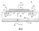
- Figure 8 illustrates a double-diffused or double-implanted MOSFET broadly designated at 60 that incorporates the insulator structure of the present invention.
- the transistor source is formed by n+ regions 61 within p-type wells 62 which are incorporated into a silicon carbide portion shown as the epitaxial layer 63 in the manner described in the above-referenced applications.
- the region 63 represents the drain drift region of the transistor with the n+ drain being illustrated at 64 , a drain contact at 65 , and an appropriate wire lead at 66 .
- the source contacts are respectively shown at 67 with their wire leads 70 .
- the gate insulator structure is formed according to the present invention and in preferred embodiments includes the first silicon dioxide layer 71 , a silicon nitride layer 72 , and a second silicon dioxide layer 73 .
- a gate metal contact 74 and its wire lead 75 complete the structure.
- the p-type regions 62 are depleted to form an inversion layer when a bias is applied to the gate contact 74 .
- the drain portion 64 were to be changed in this structure from n+ conductivity to p-type conductivity, the resulting illustration would represent an insulated gate bipolar transistor (IGBT).
- IGBT insulated gate bipolar transistor
- the illustrated structures may improve the gate or field passivation by layering the second dielectric material over the silicon dioxide.
- the silicon dioxide continues to provide a large electrical barrier (i.e ., its 9 eV bandgap) on silicon carbide and prevents the layered dielectric from leaking current.
- the additional dielectric material (with its higher dielectric constant) improves the high temperature and high field reliability as compared to a single dielectric layer.
- the layered dielectric combines the functional strengths of the two different materials to form a better dielectric on silicon carbide than could be attained with a single material.
- silicon dioxide forms a better interface, in terms of electrically charged or active states, with silicon carbide than does any other dielectric material.
- the dielectric constant of the material selected to be layered with the silicon dioxide is an important consideration because the field in the dielectric will be directly related to the field in the nearby silicon carbide and further related to the ratio of the dielectric constants of the layered dielectric and the silicon carbide.
- Table 1 summarizes the dielectric constant for some common semiconductor devices and also lists silicon carbide as the figure of merit.
- the Critical Field represents the field strength at which the material will break down immediately.
- the Operating Field (E O ) is the highest field that is expected to cause little or no degradation to the dielectric for a satisfactory time period, e.g ., at least 10 years.
- Embodiments of the present invention may improve the reliability of the gate or field passivation on silicon carbide by utilizing a dielectric material with a higher dielectric constant than silicon dioxide.
- Gauss' Law requires the field in the dielectric to be the field in the semiconductor multiplied by a factor of ( ⁇ semiconductor / ⁇ dielectric ). Accordingly, materials with dielectric constants higher than the dielectric constant of silicon carbide will have a lower electric field than the nearby silicon carbide. Accordingly, a critical measure of a material's applicability as a gate dielectric or passivating material for power devices is the product of field strength (E) and dielectric constant ( ⁇ ). Ideally the product of ⁇ E would exceed that of silicon carbide.
- Table 1 lists several dielectrics that could be potentially layered with silicon dioxide to create an insulator structure that has better electrical characteristics than either of the two materials alone. Nevertheless, additional materials may be used in a dielectric structure and the selection is not limited to those in Table 1.
- the layered dielectric of the invention has four important characteristics that enable silicon carbide MIS devices to operate at high temperatures or at high gate voltages: First, the bulk of the dielectric can be deposited, thus avoiding thermal consumption of SiC. As noted earlier, thermally grown silicon dioxide tends to consume silicon carbide more rapidly over implanted regions thus resulting in a physical step and higher fields at the edge of an implanted region. Second, the SiO 2 portion of the insulator structure has a high quality interface with silicon carbide. Third, the multilayer structure minimizes leakage currents at high temperatures (250-400°C). Fourth, the non-SiO 2 portion contributes a relatively high dielectric constant thus lowering the field in the non-SiO 2 dielectric as dictated by Gauss' Law.
- the physical thickness of the layered dielectric of the invention generally will be different than that of a single dielectric layer, with the difference being determined by the ratios of the dielectric constants.
- the layered dielectric is most preferably structured with silicon dioxide as the bottom layer (i.e ., the one in contact with the silicon carbide), because this is required for acceptable leakage currents at high temperatures.
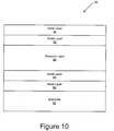
- Figure 10 illustrates a structure of a MIM capacitor 80 according to embodiments of the present invention.
- a metal layer 84 is formed on a substrate 82 , such as a silicon carbide substrate as described above.
- the metal layer 84 may be any suitable conducting material such as aluminum, gold, titanium, chromium or the like, however, in particular, titanium-platinum-gold metal layers may be utilized.
- An oxide layer 86 such as silicon dioxide, is formed on the metal layer 84 by, for example, CVD.
- a second metal layer 92 is formed on the second oxide layer 90 .
- each of the layers 86 , 88 and 90 are deposited layers.
- the capacitor is provided in combination with silicon carbide semiconductor devices.
- at least one of the metal layers 84 and 92 is formed on a silicon carbide substrate, with or without intervening layers.
- the characteristics of silicon carbide as a high voltage, high temperature material may be advantageously exploited.
- the metal layers 84 and 92 may be titanium, platinum, chromium and/or gold.
- the oxide layers 86 and 90 are silicon dioxide and the layer of dielectric material 88 is silicon nitride or oxynitride
- the silicon dioxide layers be at least about an order of magnitude thinner than the silicon nitride or oxynitride layer.
- the silicon dioxide layers may be from about 10 to about 30 nm in thickness and the silicon nitride or oxynitride layer be from about 200 to about 300 nm in thickness.
- thicknesses of the oxide layers should be relatively small so as to provide a high dielectric constant for the total structure.
- differing thicknesses of the oxide and high dielectric layers may be selected so as to provide an overall dielectric constant suitable for a particular application.
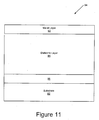
- Figure 11 illustrates further embodiments of the present invention which provide a capacitor 94 having an oxynitride as the dielectric material.
- a silicon carbide substrate 82 has a layer 98 formed thereon.
- the layer 98 is a silicon carbide layer, such as an epitaxial layer.
- the layer 98 is a metal layer such as described above with reference to the metal layer 84 of Figure 10 .
- the dielectric layer 96 is provided on the layer 98 and is disposed between a metal layer 92 and the layer 98 .
- the dielectric layer 96 is an oxynitride.
- Oxynitride refers to a nitride layer deposited in the presence of an oxygen precursor, such as nitrous oxide (N 2 O), thereby introducing oxygen into the layer.
- the dielectric layer 96 is a nitride film that has been oxygenated. The oxygenation results in greater dielectric strength (higher breakdown) without necessarily sacrificing the high dielectric constant.
- the dielectric layer 96 may be an oxynitride, such as silicon oxynitride and preferably is a silicon oxynitride of the formula Si 3 N 4-X O X , where 0 ⁇ X ⁇ 1.
- the thickness of the dielectric layer 96 may depend on the desired characteristics of the capacitor. However, in general thicknesses of from about 20 nm to about 400nm may be suitable for capacitors for use on silicon carbide substrates.
- Dielectric layers 98 may be provided, for example, by PECVD utilizing a silicon precursor, such as SiH 4 , a nitrogen precursor, such as N 2 , and an oxygen precursor, such as N 2 O. Additionally, an inert gas, such as He or Ar, may also be utilized in the PECVD process. Furthermore, other silicon, nitrogen and oxygen precursors may also be utilized while still benefiting from the teachings of the present invention.
- a silicon precursor such as SiH 4
- N 2 such as N 2
- an oxygen precursor such as N 2 O
- an inert gas such as He or Ar
- other silicon, nitrogen and oxygen precursors may also be utilized while still benefiting from the teachings of the present invention.
- a dielectric layer 98 may be formed to a thickness of 250 ⁇ in 2 minutes and 30 seconds at a deposition rate of 10 nm per minute utilizing SiH 4 at a flow rate of 300 standard cubic centimeters per minute (SCCM), N 2 O at a flow rate of 10 SCCM, N 2 at a flow rate of 150 SCCM, He at a flow rate of 200 SCCM, a power of 20 watts, a pressure of 900 mT and a temperature of 250 °C.
- SCCM standard cubic centimeters per minute
- N 2 O at a flow rate of 10 SCCM
- N 2 at a flow rate of 150 SCCM
- He at a flow rate of 200 SCCM
- a power of 20 watts a pressure of 900 mT and a temperature of 250 °C.
- SiH 4 flow rates of from about 240 to about 360 SCCM, N 2 O flow rates of from about 8 to about 12 SCCM and N 2 flow rates of from about 120 to about 180 SCCM may be utilized.
- He is provided as an inert gas
- flow rates of from about 160 to about 240 SCCM may be utilized.
- powers of from about 16 to about 24 watts, pressures of from about 720 to 1080 mT and temperatures of from about 200 to 300 °C may also be utilized.
- the above processing parameters are provided with reference to use of the above described PECVD apparatus. Different processing parameters equivalent to those described above may be utilized with differing PECVD equipment to provide oxynitride layers according to embodiments of the present invention.
- Embodiments of the present invention as illustrated in Figures 10 and 11 may provide for improved mean time to failure over conventional nitride only devices.
- Devices according to embodiments of the present invention may provide mean time to failures of about 10 6 , about 10 7 or even greater, for desired operating parameters.
- MIM capacitors according to embodiments of the present invention have a mean time to failure of at least about 10 7 hours at a voltage of up to about 50 volts and a temperature of about 100 °C. More preferably, such capacitors have a mean time failure of at least about 10 6 and most preferably about 10 7 hours or at a voltage of up to about 100 volts and a temperature of about 100 °C.
- a substrate 118 such as a silicon carbide substrate, may have a plurality of semiconductor devices 120 formed therein.
- An insulating layer may be provided on the semiconductor devices 120 and an interconnection layer having a plurality of regions of interconnect metal 124 provided on the insulating layer 122 .
- a dielectric structure 140 may be provide on the regions of interconnect metal 124 .
- a first oxide layer 142 is provided on the regions of interconnect metal 124 and a layer of dielectric material 144 is provided on the first oxide layer 142 opposite the regions of interconnect metal 124 .
- a second oxide layer 146 is provided on the layer of dielectric material opposite the first oxide layer 142 .
- the layer of dielectric material 144 may have a higher dielectric constant than that of the oxide layers 142 and 146 .
- a second interconnect layer having regions of interconnect metal 126 may be provided on the second oxide layer 146 opposite the layer of dielectric material 144 .
- an insulating layer 128 may be provided on the second interconnect layer.
- a plurality of dielectric structures, such as the structure 140 may be provided between 3 or more metallization layers. Accordingly, embodiments of the present invention may provide for one or more inter-metal dielectric regions having a dielectric structure according to embodiments of the present invention.
- the dielectric structure 140 of Figure 14 may be provided as described above with respect to the dielectric structure of the MIM capacitor of Figure 10 or the capacitor of Figure 11 .
- the metal layer 84 may be considered a region of a first interconnect layer having interconnect metal and metal layer 92 may be considered a region of a second interconnect layer having interconnect metal such that the dielectric structure of Figure 10 is disposed between the corresponding regions of interconnect metal.
- the dielectric structure 140 may be a single layer of oxynitride as illustrated in Figure 11 .
- Such dielectric structures may be selectively located at "cross-over” points of the metal regions of the interconnect structure or the oxide, high dielectric material and oxide layers may be "blanket” deposited over the first interconnect layer and the second interconnect layer formed on the blanket deposited dielectric structure.
- the high mean time to failure benefits of the structure illustrated in Figures 10 and 11 may, thus, also be provided in interconnect structures for integrated circuits.
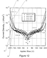
- FIG. 10 MIM capacitors according to embodiments illustrated in Figure 10 were fabricated by a CVD process with varying thicknesses of silicon dioxide and silicon nitride.
- Figure 12 is a graph of current density for versus applied bias for a MIM capacitor having only silicon nitride as its dielectric (line 100 ), a MIM capacitor having a silicon dioxide layers of 30 nm surrounding a silicon nitride layer of 300 nm (line 106 ), a MIM capacitor having a silicon dioxide layers of 10 nm surrounding a silicon nitride layer of 300 nm (line 104 ) and a MIM capacitor having a silicon dioxide layers of 20 nm surrounding a silicon nitride layer of 200 nm (line 102 ).
- the capacitance per unit area ranged from 1.98 to 2.15 with the highest capacitance being for the nitride only capacitor and the lowest capacitance for the 30/300/30 capacitor corresponding to line 106.
- the capacitance of the other devices was 2.02.
- Each of the capacitors had an area of 1.6 x 10 -3 cm 2 except for the 20/260/20 capacitor which had an area of 9 x 10 -4 cm 2 .
- the capacitors according to embodiments of the present invention exhibited reduced leakage currents at high voltages over the capacitor having only a nitride dielectric layer.
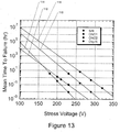
- Figure 13 is graph of stress voltage versus mean time to failure for a capacitor having only a nitride dielectric (line 112 ) and a capacitor according to embodiments of the present invention having silicon dioxide layers of 30 nm in thickness and a silicon nitride layer of 300 nm in thickness (line 110 ), a capacitor having silicon dioxide layers of 30 nm in thickness and a silicon nitride layer of 240 nm in thickness (line 114 ) and a capacitor having a silicon oxynitride layer of 350 nm in thickness (line 116 ).
- Mean time to failure was developed by testing devices at various stress voltages and determining the average of failure times as a result of intrinsic defects (i.e.
- Capacitors were fabricated using the materials in Table 2 and including those of the present invention.
- a three-step process was used to produce respective silicon dioxide, silicon nitride, and silicon dioxide layers.
- high quality silicon dioxide was thermally grown on silicon carbide in an oxidation furnace to a thickness of about 100 angstroms ( ⁇ ).
- a preferred oxidation technique is set forth in co-pending and commonly assigned application Serial No. 08/554,319, filed November 8, 1995 , for "Process for Reducing Defects in Oxide Layers on Silicon Carbide," the contents of which are incorporated entirely herein by reference.
- nitride layer was deposited using low pressure chemical vapor deposition (LPCVD) with silane (SiH 4 ) and ammonia (NH 3 ) as the source gases.
- LPCVD low pressure chemical vapor deposition
- SiH 4 silane
- NH 3 ammonia
- This nitride layer was then oxidized in a wet ambient atmosphere at 950°C for three hours to form a second layer of silicon dioxide that was between about 50 and 100 angstroms thick.
- a dielectric must have high reliability for high temperature high field device passivation applications, such reliability represents a necessary, but not a sufficient characteristic, to make it applicable for the gate layer of a MIS device.
- charged bulk defects and electrically active interface defects must be minimized. Charged bulk defects will tend to cause voltage shifts in the device, while electrically active interface defects will degrade the channel mobility.
- Fixed oxide charge Charged bulk defects are traditionally referred to as "fixed oxide charge” and are measured by the flatband voltage determined by a room temperature high frequency capacitance-voltage (CV) curve. Any difference between the actual voltage at which flatband capacitance occurs and the ideal value, accounting for metal-semiconductor work functions, is attributed to this fixed oxide charge.
- CV capacitance-voltage
- the term "fixed” oxide charge is a misnomer. This calculated charge density includes contributions from interface states, many of which appear fixed at room temperature. For this reason, this calculated charge density is referred to herein as a "net” oxide charge.
- interface states Electrically active defects at the dielectric-semiconductor interface are termed interface states. These states can severely degrade the channel mobility of an MIS devices by either trapping and releasing the electrons, or by providing a charged site which would apply a force normal to the current flow. Either of these effects will inhibit current flow and subsequently reduce the channel mobility.
- Table 3 compares the net oxide charge densities and minimum measured interface state densities of the various capacitors.
- Table 3 Net Oxide Charge (10 11 cm -2 ) Insulator 6H P-type 6H N-type 4H N-type Thermal SiO 2 6.9 -10.8 -26 LPCVD SiO 2 7.5 -11.5 -29 Silicon Nitride Leaky -9.7 -51 ONO 130 1.9 5.9 AlN 64 -26 -54 AlO:N 8.9 1.3 -5.2 Interface State Densities (10 10 cm -2 eV -1 ) Insulator 6H P-type 6H N-type 4H N-type Thermal SiO 2 6.2 36 210 LPCVD SiO 2 7.5 18 270 Silicon Nitride Leaks 240 1500 ONO 74 5.7 14 AlN 650 leaks leaks AlO:N ⁇ 50 leaks leaks
- the net oxide charge and interface state densities are the lowest on thermal - oxides and the LPCVD oxides, with no significant differences seen between these samples.
- the net oxide charge and interface state densities are significantly lower on the silicon dioxide/silicon nitride/silicon dioxide sample (also referred to herein as "ONO" structures).
- the silicon carbide/insulator interface quality is obviously superior when silicon dioxide forms the interface with the silicon carbide.
- the silicon dioxide layers had the highest breakdown fields, especially at high temperature, regardless of the manner in which they were grown or deposited.
- the 1100°C thermally grown oxides had the highest breakdown fields, with the deposited oxides being almost as high.
- E B breakdown fields
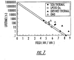
- Time-bias measurements at 350°C taken on 6H n-type SiC MIS capacitors are shown in Figure 7 .
- the measured points are shown by the symbols, and the exponential least squares fit is shown by the lines.
- the lifetimes exhibited by these devices are low, which is partially due to the small sample size. However, these values are not atypical for oxides on n-type SiC at 350°C.
- the ONO capacitors had the highest lifetimes, showing more than an order of magnitude improvement in lifetime over both the deposited and thermal oxides at a given applied electric field.
- the p-type interface quality of ONO capacitors is not as good as the thermal or deposited oxides, the n-type interface quality is better than any of the other materials.
- MISFETs planar metal-insulator semiconductor field effect transistors
- thermal oxidation results in a physical step, as the implanted source and drain regions oxidize faster than the non-implanted channel region. Thermal oxides grown on implanted areas also tend to be weaker than those grown on non-implanted material. These two effects are combined in a thermally oxidized MOSFET, where the step enhances the field and the region of the weakest oxide. Thus the breakdown field of the thermally oxidized MOSFET is significantly reduced from the breakdown fields demonstrated by the MOS capacitors.
- the deposited oxide has a higher breakdown field than the thermally grown oxide, but the highest breakdown voltage was achieved with the ONO dielectric layers.
- the field was slightly low at 350°C, but the breakdown voltage is probably a better indicator of device reliability because a silicon nitride gate insulator must be thicker in order to have the same gate capacitance.
- the ONO structure demonstrated almost double the high temperature breakdown voltage of the thermally oxidized devices.
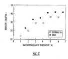
- the channel mobility of the fat FETs (a "fat" FET has a large gate width approximately equal to its gate length) was determined from the linear regime of the MISFET: The drain voltage was set at 0.25 volts, and the gate voltages stepped from 0 to 10 volts in one volt steps. The mobility was calculated from the conductance between the various gate voltages, which is independent of the threshold voltage.
- Figure 5 compares the channel mobility of the MISFETs fabricated with layered ONO dielectrics to those with thermal oxides. The ONO MISFETs have a slightly higher mobility. Figure 5 , thus, shows that the ONO layered dielectric structure is at least as good as a thermal oxide in these devices.
- An estimate of the MISFET device reliability at high temperatures was measured by applying a gate voltage of 15V (3 MV/cm) to a 4 x 100 ⁇ m gate, grounding the source, drain and substrate, and monitoring the gate current until a compliance current of 1 nA was reached. This compliance current corresponds to a current density of 0.25 mA/cm 2 .
- the gate voltage was increased above the probable use-voltage of 5 V to accelerate this test.
- Table 6 compares the high temperature reliability of the MISFETs fabricated with layered ONO dielectrics with those having thermal and deposited silicon dioxide.
- the ONO MOSFETs have a significantly better high temperature lifetime, e.g., more than a factor of 100x better.
- a packaged MISFET operated successfully for 240 hours. TABLE 6 Device lifetimes at 350°C with a 15 V (3 MV/cm) gate bias Insulator Lifetime Dry Thermal Oxide 0.08 hour Deposited Oxide 0.75 hour ONO > 75 hours ONO (Packaged, Estimated 335°C) 240 hours
- the ONO sample was wafer tested at 350°C for 75 hours without failing. At that point, it was decided to package devices for testing, because the device metals would oxidize if exposed to air for several days at 350°C. The packaged parts were then tested at 350°C. The exact temperature of the packaged devices could not be easily controlled, however, and thus the estimated testing temperature was probably closer to 335°C than to 350°C. Nevertheless, the ONO sample survived for 10 days (240 hours) at 335°C.
- Figure 9 also shows the MISFET lifetimes for comparison with the capacitor results.
- the MISFETs with the dry-wet thermal oxide have a dramatically reduced lifetime when compared with the capacitors. This is most likely due to the physical steps created at the source and drain regions by the accelerated growth of the implanted regions.
- the deposited oxide MISFET failed very close to its projected time, but slightly lower.
- the ONO MISFET fails almost exactly where one would predict from the MIS capacitor data.
- a 4-wafer lot of planar diodes was fabricated.
- a cross section of an exemplary device 50 is shown in Figure 6 .
- the top p-layer 51 was implanted with variable doses.
- a second implant, the Junction Termination Extension (JTE) 52 was performed adjacent to the first implant to reduce field crowding.
- JTE Junction Termination Extension
- the JTE implant helps reduce the field crowding at the edge of the device, a high quality dielectric 53 on the surface of the wafer is required for passivation.
- the shape of the planar diode was circular.
- the dielectric 53 is formed of the oxide/nitride/oxide according to the present invention. Specifically, all three layers were deposited by PECVD.
- the mask set used for this device consisted of diodes with radii varying from 100 to 500 ⁇ m, while the width of the JTE implant varied between 50 and 150 ⁇ m.
- the epitaxial layers should support 5 kV, but the JTE of these devices were designed to block only 3 kV in order to place more stress on the passivation.
- the device performance is more sensitive to the passivation, because the JTE implants do not terminate all of the fields generated by the higher voltage. Accordingly, the passivation must withstand much larger fields.
- the devices were deliberately designed to help evaluate the various dielectric materials.
- n-type substrates for these devices had a 50 ⁇ m epitaxial n - layer doped about 1x10 15 cm -3 grown, and a 1.2 ⁇ m p - layer doped 1x10 18 cm -3 .
- Figure 6 also illustrates the n-type portion of the device at 54 , the anode at 55 , and the cathode at 56 .
- the fabrication of the diode began with etching alignment marks into the SiC wafer for alignment of the future masks.
- the anode junction was defined by etching through the top p-type layer in most of the surface, while leaving circular p-type anode regions exposed.
- a thick (1.4 ⁇ m) oxide mask the regions receiving the low-dose JTE implant were defined.
- the thickness of the oxide mask and the implantation energy and dosage of the p-type dopant (aluminum) were chosen so that only the intended termination region receives the implant while it is blocked entirely from regions where it is not intended.
- the junction region also received this implantation step so that a high surface doping of the p-type layer was formed for ohmic anode contacts.
- the implanted aluminum was annealed to minimize the damage from ion implantation and to electrically activate the implants.
- the breakdown voltage was measured on each type of diode.
- the silicon nitride had a great deal of leakage, and broke down at 2.6 kV.
- the oxide devices had low/no leakage and broke down around 3.5 kV.
- the devices incorporating the dielectric structure of the invention had no leakage out to 5 kV, and broke at a world-record level of 5.9 kV.
- the ONO dielectric of the present invention provides a significant improvement.
- the high temperature lifetime of the ONO layered MISFET is more than a factor of 100x better than the state-of-the-art deposited oxide. This has immediate relevance to high temperature SiC power devices and circuits. By projecting back to the likely rated operating field of 1 MV/cm, it can be predicted that ONO MOSFETs will have a lifetime of more than 240,000 hours at 335°C.
Landscapes
- Engineering & Computer Science (AREA)
- Power Engineering (AREA)
- Microelectronics & Electronic Packaging (AREA)
- Manufacturing & Machinery (AREA)
- Chemical & Material Sciences (AREA)
- Condensed Matter Physics & Semiconductors (AREA)
- Crystallography & Structural Chemistry (AREA)
- Physics & Mathematics (AREA)
- Ceramic Engineering (AREA)
- General Physics & Mathematics (AREA)
- Computer Hardware Design (AREA)
- Inorganic Chemistry (AREA)
- Semiconductor Integrated Circuits (AREA)
- Fixed Capacitors And Capacitor Manufacturing Machines (AREA)
- Insulated Gate Type Field-Effect Transistor (AREA)
Applications Claiming Priority (3)
| Application Number | Priority Date | Filing Date | Title |
|---|---|---|---|
| US09/878,442 US6972436B2 (en) | 1998-08-28 | 2001-06-11 | High voltage, high temperature capacitor and interconnection structures |
| US878442 | 2001-06-11 | ||
| PCT/US2002/009393 WO2002101767A2 (en) | 2001-06-11 | 2002-03-26 | High voltage, high temperature capacitor structures and methods of fabricating same |
Publications (2)
| Publication Number | Publication Date |
|---|---|
| EP1412970A2 EP1412970A2 (en) | 2004-04-28 |
| EP1412970B1 true EP1412970B1 (en) | 2019-01-09 |
Family
ID=25372039
Family Applications (1)
| Application Number | Title | Priority Date | Filing Date |
|---|---|---|---|
| EP02728581.6A Expired - Lifetime EP1412970B1 (en) | 2001-06-11 | 2002-03-26 | High voltage, high temperature capacitor structures and methods of fabricating same |
Country Status (8)
| Country | Link |
|---|---|
| US (2) | US6972436B2 (enExample) |
| EP (1) | EP1412970B1 (enExample) |
| JP (2) | JP5004406B2 (enExample) |
| KR (1) | KR100949844B1 (enExample) |
| CN (1) | CN1266742C (enExample) |
| AU (1) | AU2002258625A1 (enExample) |
| CA (1) | CA2448006C (enExample) |
| WO (1) | WO2002101767A2 (enExample) |
Families Citing this family (85)
| Publication number | Priority date | Publication date | Assignee | Title |
|---|---|---|---|---|
| US6956238B2 (en) * | 2000-10-03 | 2005-10-18 | Cree, Inc. | Silicon carbide power metal-oxide semiconductor field effect transistors having a shorting channel and methods of fabricating silicon carbide metal-oxide semiconductor field effect transistors having a shorting channel |
| WO2003047000A1 (en) * | 2001-11-30 | 2003-06-05 | Matsushita Electric Industrial Co., Ltd. | Semiconductor device and production method therefor |
| DE10217566A1 (de) * | 2002-04-19 | 2003-11-13 | Infineon Technologies Ag | Halbleiterbauelement mit integrierter, eine Mehrzahl an Metallisierungsebenen aufweisende Kapazitätsstruktur |
| US7084423B2 (en) | 2002-08-12 | 2006-08-01 | Acorn Technologies, Inc. | Method for depinning the Fermi level of a semiconductor at an electrical junction and devices incorporating such junctions |
| US6833556B2 (en) | 2002-08-12 | 2004-12-21 | Acorn Technologies, Inc. | Insulated gate field effect transistor having passivated schottky barriers to the channel |
| US7022378B2 (en) * | 2002-08-30 | 2006-04-04 | Cree, Inc. | Nitrogen passivation of interface states in SiO2/SiC structures |
| TWI320571B (en) * | 2002-09-12 | 2010-02-11 | Qs Semiconductor Australia Pty Ltd | Dynamic nonvolatile random access memory ne transistor cell and random access memory array |
| US7221010B2 (en) * | 2002-12-20 | 2007-05-22 | Cree, Inc. | Vertical JFET limited silicon carbide power metal-oxide semiconductor field effect transistors |
| US7026650B2 (en) * | 2003-01-15 | 2006-04-11 | Cree, Inc. | Multiple floating guard ring edge termination for silicon carbide devices |
| US9515135B2 (en) * | 2003-01-15 | 2016-12-06 | Cree, Inc. | Edge termination structures for silicon carbide devices |
| KR100520600B1 (ko) * | 2003-02-17 | 2005-10-10 | 주식회사 하이닉스반도체 | 반도체소자의 캐패시터 제조방법 |
| JP2004319907A (ja) * | 2003-04-18 | 2004-11-11 | Tadahiro Omi | 半導体装置の製造方法および製造装置 |
| US7074643B2 (en) * | 2003-04-24 | 2006-07-11 | Cree, Inc. | Silicon carbide power devices with self-aligned source and well regions and methods of fabricating same |
| US6979863B2 (en) * | 2003-04-24 | 2005-12-27 | Cree, Inc. | Silicon carbide MOSFETs with integrated antiparallel junction barrier Schottky free wheeling diodes and methods of fabricating the same |
| US6812110B1 (en) * | 2003-05-09 | 2004-11-02 | Micron Technology, Inc. | Methods of forming capacitor constructions, and methods of forming constructions comprising dielectric materials |
| KR100947064B1 (ko) * | 2003-08-13 | 2010-03-10 | 삼성전자주식회사 | 반도체 장치의 커패시터 및 이를 구비하는 메모리 장치 |
| CN1864268A (zh) * | 2003-09-02 | 2006-11-15 | 埃皮泰克帝斯克有限公司 | 具有隧道式mis发射结的异质结双极晶体管 |
| US7709403B2 (en) * | 2003-10-09 | 2010-05-04 | Panasonic Corporation | Silicon carbide-oxide layered structure, production method thereof, and semiconductor device |
| US7155359B1 (en) * | 2004-07-02 | 2006-12-26 | Advanced Micro Devices, Inc. | Determination of device failure characteristic |
| US7247550B2 (en) * | 2005-02-08 | 2007-07-24 | Teledyne Licensing, Llc | Silicon carbide-based device contact and contact fabrication method |
| DE102005008195A1 (de) * | 2005-02-23 | 2006-08-24 | Atmel Germany Gmbh | Hochfrequenzanordnung |
| US7619298B1 (en) * | 2005-03-31 | 2009-11-17 | Xilinx, Inc. | Method and apparatus for reducing parasitic capacitance |
| US7855401B2 (en) | 2005-06-29 | 2010-12-21 | Cree, Inc. | Passivation of wide band-gap based semiconductor devices with hydrogen-free sputtered nitrides |
| US7525122B2 (en) * | 2005-06-29 | 2009-04-28 | Cree, Inc. | Passivation of wide band-gap based semiconductor devices with hydrogen-free sputtered nitrides |
| US7598576B2 (en) * | 2005-06-29 | 2009-10-06 | Cree, Inc. | Environmentally robust passivation structures for high-voltage silicon carbide semiconductor devices |
| JP2007066944A (ja) | 2005-08-29 | 2007-03-15 | Nissan Motor Co Ltd | 炭化珪素半導体装置及びその製造方法 |
| US7340360B1 (en) * | 2006-02-08 | 2008-03-04 | Advanced Micro Devices, Inc. | Method for determining projected lifetime of semiconductor devices with analytical extension of stress voltage window by scaling of oxide thickness |
| US7478562B2 (en) * | 2006-05-05 | 2009-01-20 | Kulite Semiconductor Products, Inc. | High temperature LC pressure transducer and methods for making the same |
| US8372697B2 (en) | 2006-05-08 | 2013-02-12 | University Of South Carolina | Digital oxide deposition of SiO2 layers on wafers |
| US7728402B2 (en) * | 2006-08-01 | 2010-06-01 | Cree, Inc. | Semiconductor devices including schottky diodes with controlled breakdown |
| US8432012B2 (en) | 2006-08-01 | 2013-04-30 | Cree, Inc. | Semiconductor devices including schottky diodes having overlapping doped regions and methods of fabricating same |
| EP2631951B1 (en) | 2006-08-17 | 2017-10-11 | Cree, Inc. | High power insulated gate bipolar transistors |
| US20080157291A1 (en) * | 2006-12-27 | 2008-07-03 | Texas Instruments Inc. | Packaging implementation while mitigating threshold voltage shifting |
| US8835987B2 (en) * | 2007-02-27 | 2014-09-16 | Cree, Inc. | Insulated gate bipolar transistors including current suppressing layers |
| US8318562B2 (en) * | 2007-04-02 | 2012-11-27 | University Of South Carolina | Method to increase breakdown voltage of semiconductor devices |
| US9634191B2 (en) | 2007-11-14 | 2017-04-25 | Cree, Inc. | Wire bond free wafer level LED |
| US8431962B2 (en) * | 2007-12-07 | 2013-04-30 | Northrop Grumman Systems Corporation | Composite passivation process for nitride FET |
| US9024327B2 (en) | 2007-12-14 | 2015-05-05 | Cree, Inc. | Metallization structure for high power microelectronic devices |
| US8232558B2 (en) | 2008-05-21 | 2012-07-31 | Cree, Inc. | Junction barrier Schottky diodes with current surge capability |
| CN101364481B (zh) * | 2008-09-23 | 2010-12-15 | 宁波碧彩实业有限公司 | 带整流装置的高压电容器 |
| US8106487B2 (en) | 2008-12-23 | 2012-01-31 | Pratt & Whitney Rocketdyne, Inc. | Semiconductor device having an inorganic coating layer applied over a junction termination extension |
| US8288220B2 (en) | 2009-03-27 | 2012-10-16 | Cree, Inc. | Methods of forming semiconductor devices including epitaxial layers and related structures |
| US8294507B2 (en) | 2009-05-08 | 2012-10-23 | Cree, Inc. | Wide bandgap bipolar turn-off thyristor having non-negative temperature coefficient and related control circuits |
| US8193848B2 (en) | 2009-06-02 | 2012-06-05 | Cree, Inc. | Power switching devices having controllable surge current capabilities |
| US8629509B2 (en) * | 2009-06-02 | 2014-01-14 | Cree, Inc. | High voltage insulated gate bipolar transistors with minority carrier diverter |
| US8541787B2 (en) * | 2009-07-15 | 2013-09-24 | Cree, Inc. | High breakdown voltage wide band-gap MOS-gated bipolar junction transistors with avalanche capability |
| US8191217B2 (en) | 2009-08-05 | 2012-06-05 | International Business Machines Corporation | Complimentary metal-insulator-metal (MIM) capacitors and method of manufacture |
| US8375539B2 (en) | 2009-08-05 | 2013-02-19 | International Business Machines Corporation | Method of manufacturing complimentary metal-insulator-metal (MIM) capacitors |
| US8354690B2 (en) | 2009-08-31 | 2013-01-15 | Cree, Inc. | Solid-state pinch off thyristor circuits |
| US9117739B2 (en) | 2010-03-08 | 2015-08-25 | Cree, Inc. | Semiconductor devices with heterojunction barrier regions and methods of fabricating same |
| US8415671B2 (en) | 2010-04-16 | 2013-04-09 | Cree, Inc. | Wide band-gap MOSFETs having a heterojunction under gate trenches thereof and related methods of forming such devices |
| US8683420B2 (en) | 2010-11-17 | 2014-03-25 | Intermolecular, Inc. | Method and system of improved reliability testing |
| US9029945B2 (en) | 2011-05-06 | 2015-05-12 | Cree, Inc. | Field effect transistor devices with low source resistance |
| US9142662B2 (en) | 2011-05-06 | 2015-09-22 | Cree, Inc. | Field effect transistor devices with low source resistance |
| US9269580B2 (en) | 2011-06-27 | 2016-02-23 | Cree, Inc. | Semiconductor device with increased channel mobility and dry chemistry processes for fabrication thereof |
| US9640617B2 (en) | 2011-09-11 | 2017-05-02 | Cree, Inc. | High performance power module |
| US8680587B2 (en) | 2011-09-11 | 2014-03-25 | Cree, Inc. | Schottky diode |
| US9373617B2 (en) | 2011-09-11 | 2016-06-21 | Cree, Inc. | High current, low switching loss SiC power module |
| WO2013036370A1 (en) | 2011-09-11 | 2013-03-14 | Cree, Inc. | High current density power module comprising transistors with improved layout |
| US8664665B2 (en) | 2011-09-11 | 2014-03-04 | Cree, Inc. | Schottky diode employing recesses for elements of junction barrier array |
| US8618582B2 (en) | 2011-09-11 | 2013-12-31 | Cree, Inc. | Edge termination structure employing recesses for edge termination elements |
| JP6042656B2 (ja) | 2011-09-30 | 2016-12-14 | 株式会社日立国際電気 | 半導体装置の製造方法、基板処理方法、基板処理装置およびプログラム |
| WO2013077954A1 (en) | 2011-11-23 | 2013-05-30 | Acorn Technologies, Inc. | Improving metal contacts to group iv semiconductors by inserting interfacial atomic monolayers |
| JP5460768B2 (ja) * | 2012-03-21 | 2014-04-02 | 日産自動車株式会社 | 炭化珪素半導体装置の製造方法 |
| US8779509B2 (en) | 2012-07-02 | 2014-07-15 | Infineon Technologies Austria Ag | Semiconductor device including an edge area and method of manufacturing a semiconductor device |
| JP5646569B2 (ja) * | 2012-09-26 | 2014-12-24 | 株式会社東芝 | 半導体装置 |
| US9991399B2 (en) | 2012-10-04 | 2018-06-05 | Cree, Inc. | Passivation structure for semiconductor devices |
| US9812338B2 (en) | 2013-03-14 | 2017-11-07 | Cree, Inc. | Encapsulation of advanced devices using novel PECVD and ALD schemes |
| US8994073B2 (en) | 2012-10-04 | 2015-03-31 | Cree, Inc. | Hydrogen mitigation schemes in the passivation of advanced devices |
| CN103199081B (zh) * | 2013-04-09 | 2015-12-23 | 上海华力微电子有限公司 | Mim电容器及其制造方法 |
| US9515211B2 (en) * | 2013-07-26 | 2016-12-06 | University Of South Carolina | Schottky barrier detection devices having a 4H-SiC n-type epitaxial layer |
| CN104465608A (zh) * | 2013-09-23 | 2015-03-25 | 中芯国际集成电路制造(上海)有限公司 | Mim电容器及其制造方法 |
| CN104037240A (zh) * | 2014-06-26 | 2014-09-10 | 西安电子科技大学 | SiC MOS电容及制造方法 |
| CN104037239A (zh) * | 2014-06-26 | 2014-09-10 | 西安电子科技大学 | SiC MOS电容及制造方法 |
| CN104037238A (zh) * | 2014-06-26 | 2014-09-10 | 西安电子科技大学 | SiC MOS电容及制造方法 |
| US9461108B2 (en) * | 2014-08-13 | 2016-10-04 | Fairchild Semiconductor Corporation | SiC power device having a high voltage termination |
| JP2016066641A (ja) * | 2014-09-22 | 2016-04-28 | 株式会社東芝 | 半導体装置及び半導体装置の製造方法 |
| US9620611B1 (en) | 2016-06-17 | 2017-04-11 | Acorn Technology, Inc. | MIS contact structure with metal oxide conductor |
| WO2018094205A1 (en) | 2016-11-18 | 2018-05-24 | Acorn Technologies, Inc. | Nanowire transistor with source and drain induced by electrical contacts with negative schottky barrier height |
| US10319582B2 (en) * | 2017-04-27 | 2019-06-11 | Lam Research Corporation | Methods and apparatus for depositing silicon oxide on metal layers |
| US9998109B1 (en) * | 2017-05-15 | 2018-06-12 | Cree, Inc. | Power module with improved reliability |
| CN109887746B (zh) * | 2019-03-06 | 2021-01-01 | 无锡鑫聚电子科技有限公司 | 一种用于高可靠大功率电容器的金属化薄膜及其制备方法 |
| CN111710658A (zh) * | 2020-07-01 | 2020-09-25 | 华虹半导体(无锡)有限公司 | 防分层mim电容及其制作方法 |
| CN111933612B (zh) * | 2020-10-09 | 2021-02-19 | 晶芯成(北京)科技有限公司 | 一种半导体结构的制造方法 |
| TWI795286B (zh) * | 2022-05-06 | 2023-03-01 | 國立陽明交通大學 | 浮動保護環耐壓的穩定方法 |
Family Cites Families (85)
| Publication number | Priority date | Publication date | Assignee | Title |
|---|---|---|---|---|
| US3924024A (en) | 1973-04-02 | 1975-12-02 | Ncr Co | Process for fabricating MNOS non-volatile memories |
| US4466172A (en) | 1979-01-08 | 1984-08-21 | American Microsystems, Inc. | Method for fabricating MOS device with self-aligned contacts |
| JPS61207048A (ja) * | 1985-03-12 | 1986-09-13 | Seiko Instr & Electronics Ltd | 半導体装置 |
| US4875083A (en) | 1987-10-26 | 1989-10-17 | North Carolina State University | Metal-insulator-semiconductor capacitor formed on silicon carbide |
| JPH01239940A (ja) * | 1988-03-22 | 1989-09-25 | Seiko Epson Corp | 半導体装置 |
| JPH0766971B2 (ja) | 1989-06-07 | 1995-07-19 | シャープ株式会社 | 炭化珪素半導体装置 |
| JPH03157974A (ja) | 1989-11-15 | 1991-07-05 | Nec Corp | 縦型電界効果トランジスタ |
| JP2542448B2 (ja) | 1990-05-24 | 1996-10-09 | シャープ株式会社 | 電界効果トランジスタおよびその製造方法 |
| JPH06160174A (ja) | 1991-09-27 | 1994-06-07 | Terumo Corp | 赤外線センサ |
| US5170455A (en) | 1991-10-30 | 1992-12-08 | At&T Bell Laboratories | Optical connective device |
| JP3356816B2 (ja) | 1992-03-24 | 2002-12-16 | セイコーインスツルメンツ株式会社 | 半導体光電気変換装置 |
| JP2704575B2 (ja) * | 1992-04-20 | 1998-01-26 | 日本電信電話株式会社 | 容量素子の製造方法 |
| US5185689A (en) | 1992-04-29 | 1993-02-09 | Motorola Inc. | Capacitor having a ruthenate electrode and method of formation |
| US6344663B1 (en) | 1992-06-05 | 2002-02-05 | Cree, Inc. | Silicon carbide CMOS devices |
| US5459107A (en) | 1992-06-05 | 1995-10-17 | Cree Research, Inc. | Method of obtaining high quality silicon dioxide passivation on silicon carbide and resulting passivated structures |
| US5726463A (en) | 1992-08-07 | 1998-03-10 | General Electric Company | Silicon carbide MOSFET having self-aligned gate structure |
| US5587870A (en) | 1992-09-17 | 1996-12-24 | Research Foundation Of State University Of New York | Nanocrystalline layer thin film capacitors |
| US5506421A (en) | 1992-11-24 | 1996-04-09 | Cree Research, Inc. | Power MOSFET in silicon carbide |
| KR100305123B1 (ko) * | 1992-12-11 | 2001-11-22 | 비센트 비.인그라시아, 알크 엠 아헨 | 정적랜덤액세스메모리셀및이를포함하는반도체장치 |
| EP0605980A3 (en) * | 1993-01-07 | 1995-08-02 | Ramtron Int Corp | Layering process for depositing silicon nitride and silicon oxynitride. |
| JPH06252347A (ja) * | 1993-02-25 | 1994-09-09 | Mitsubishi Electric Corp | Mimキャパシタ及びその製造方法 |
| US5479316A (en) * | 1993-08-24 | 1995-12-26 | Analog Devices, Inc. | Integrated circuit metal-oxide-metal capacitor and method of making same |
| US5510630A (en) | 1993-10-18 | 1996-04-23 | Westinghouse Electric Corporation | Non-volatile random access memory cell constructed of silicon carbide |
| JP3254875B2 (ja) * | 1994-02-03 | 2002-02-12 | 富士通株式会社 | 半導体装置の製造方法 |
| JP3521246B2 (ja) | 1995-03-27 | 2004-04-19 | 沖電気工業株式会社 | 電界効果トランジスタおよびその製造方法 |
| JPH0969589A (ja) * | 1995-09-01 | 1997-03-11 | Mitsubishi Materials Corp | 薄膜コンデンサ内蔵型モジュール |
| JPH11261061A (ja) | 1998-03-11 | 1999-09-24 | Denso Corp | 炭化珪素半導体装置及びその製造方法 |
| JP4001960B2 (ja) | 1995-11-03 | 2007-10-31 | フリースケール セミコンダクター インコーポレイテッド | 窒化酸化物誘電体層を有する半導体素子の製造方法 |
| US5972801A (en) | 1995-11-08 | 1999-10-26 | Cree Research, Inc. | Process for reducing defects in oxide layers on silicon carbide |
| US6136728A (en) | 1996-01-05 | 2000-10-24 | Yale University | Water vapor annealing process |
| JPH09205202A (ja) | 1996-01-26 | 1997-08-05 | Matsushita Electric Works Ltd | 半導体装置 |
| US5877045A (en) | 1996-04-10 | 1999-03-02 | Lsi Logic Corporation | Method of forming a planar surface during multi-layer interconnect formation by a laser-assisted dielectric deposition |
| US5972788A (en) | 1996-05-22 | 1999-10-26 | International Business Machines Corporation | Method of making flexible interconnections with dual-metal-dual-stud structure |
| JP3889476B2 (ja) * | 1996-05-29 | 2007-03-07 | 三菱電機株式会社 | マイクロ波半導体集積回路の製造方法 |
| JPH1022457A (ja) | 1996-07-03 | 1998-01-23 | Mitsubishi Electric Corp | 容量装置及び半導体装置並びにそれらの製造方法 |
| US5763905A (en) | 1996-07-09 | 1998-06-09 | Abb Research Ltd. | Semiconductor device having a passivation layer |
| US6002159A (en) | 1996-07-16 | 1999-12-14 | Abb Research Ltd. | SiC semiconductor device comprising a pn junction with a voltage absorbing edge |
| US5939763A (en) | 1996-09-05 | 1999-08-17 | Advanced Micro Devices, Inc. | Ultrathin oxynitride structure and process for VLSI applications |
| US6028012A (en) | 1996-12-04 | 2000-02-22 | Yale University | Process for forming a gate-quality insulating layer on a silicon carbide substrate |
| US5837572A (en) | 1997-01-10 | 1998-11-17 | Advanced Micro Devices, Inc. | CMOS integrated circuit formed by using removable spacers to produce asymmetrical NMOS junctions before asymmetrical PMOS junctions for optimizing thermal diffusivity of dopants implanted therein |
| JP3206727B2 (ja) | 1997-02-20 | 2001-09-10 | 富士電機株式会社 | 炭化けい素縦型mosfetおよびその製造方法 |
| DE19809554B4 (de) | 1997-03-05 | 2008-04-03 | Denso Corp., Kariya | Siliziumkarbidhalbleitervorrichtung |
| JPH1117027A (ja) * | 1997-06-19 | 1999-01-22 | Hitachi Ltd | 半導体記憶装置及びその製造方法 |
| US6063698A (en) | 1997-06-30 | 2000-05-16 | Motorola, Inc. | Method for manufacturing a high dielectric constant gate oxide for use in semiconductor integrated circuits |
| JP3180895B2 (ja) | 1997-08-18 | 2001-06-25 | 富士電機株式会社 | 炭化けい素半導体装置の製造方法 |
| CN1267397A (zh) | 1997-08-20 | 2000-09-20 | 西门子公司 | 具有预定的α碳化硅区的半导体结构及此半导体结构的应用 |
| US6100184A (en) | 1997-08-20 | 2000-08-08 | Sematech, Inc. | Method of making a dual damascene interconnect structure using low dielectric constant material for an inter-level dielectric layer |
| US6239463B1 (en) | 1997-08-28 | 2001-05-29 | Siliconix Incorporated | Low resistance power MOSFET or other device containing silicon-germanium layer |
| SE9704150D0 (sv) | 1997-11-13 | 1997-11-13 | Abb Research Ltd | Semiconductor device of SiC with insulating layer a refractory metal nitride layer |
| JPH11191559A (ja) | 1997-12-26 | 1999-07-13 | Matsushita Electric Works Ltd | Mosfetの製造方法 |
| JPH11251592A (ja) | 1998-01-05 | 1999-09-17 | Denso Corp | 炭化珪素半導体装置 |
| JP3216804B2 (ja) | 1998-01-06 | 2001-10-09 | 富士電機株式会社 | 炭化けい素縦形fetの製造方法および炭化けい素縦形fet |
| JPH11266017A (ja) | 1998-01-14 | 1999-09-28 | Denso Corp | 炭化珪素半導体装置及びその製造方法 |
| JPH11238742A (ja) | 1998-02-23 | 1999-08-31 | Denso Corp | 炭化珪素半導体装置の製造方法 |
| US5946567A (en) | 1998-03-20 | 1999-08-31 | Taiwan Semiconductor Manufacturing Company, Ltd. | Method for making metal capacitors for deep submicrometer processes for semiconductor integrated circuits |
| JP3893725B2 (ja) | 1998-03-25 | 2007-03-14 | 株式会社デンソー | 炭化珪素半導体装置の製造方法 |
| US6627539B1 (en) | 1998-05-29 | 2003-09-30 | Newport Fab, Llc | Method of forming dual-damascene interconnect structures employing low-k dielectric materials |
| US6107142A (en) | 1998-06-08 | 2000-08-22 | Cree Research, Inc. | Self-aligned methods of fabricating silicon carbide power devices by implantation and lateral diffusion |
| US6100169A (en) | 1998-06-08 | 2000-08-08 | Cree, Inc. | Methods of fabricating silicon carbide power devices by controlled annealing |
| JP4123636B2 (ja) | 1998-06-22 | 2008-07-23 | 株式会社デンソー | 炭化珪素半導体装置及びその製造方法 |
| US5960289A (en) | 1998-06-22 | 1999-09-28 | Motorola, Inc. | Method for making a dual-thickness gate oxide layer using a nitride/oxide composite region |
| JP2000106371A (ja) | 1998-07-31 | 2000-04-11 | Denso Corp | 炭化珪素半導体装置の製造方法 |
| US6221700B1 (en) | 1998-07-31 | 2001-04-24 | Denso Corporation | Method of manufacturing silicon carbide semiconductor device with high activation rate of impurities |
| JP3959856B2 (ja) | 1998-07-31 | 2007-08-15 | 株式会社デンソー | 炭化珪素半導体装置及びその製造方法 |
| US6246076B1 (en) | 1998-08-28 | 2001-06-12 | Cree, Inc. | Layered dielectric on silicon carbide semiconductor structures |
| US6211035B1 (en) | 1998-09-09 | 2001-04-03 | Texas Instruments Incorporated | Integrated circuit and method |
| US6204203B1 (en) | 1998-10-14 | 2001-03-20 | Applied Materials, Inc. | Post deposition treatment of dielectric films for interface control |
| US6048766A (en) | 1998-10-14 | 2000-04-11 | Advanced Micro Devices | Flash memory device having high permittivity stacked dielectric and fabrication thereof |
| JP2000201050A (ja) | 1998-11-02 | 2000-07-18 | Ngk Insulators Ltd | 表面弾性波装置用基板およびその製造方法 |
| JP3127908B2 (ja) * | 1998-11-20 | 2001-01-29 | 日本電気株式会社 | 半導体装置の製造方法 |
| JP2000183052A (ja) * | 1998-12-18 | 2000-06-30 | Sony Corp | 電子装置の製造方法 |
| US6190973B1 (en) | 1998-12-18 | 2001-02-20 | Zilog Inc. | Method of fabricating a high quality thin oxide |
| US6228720B1 (en) | 1999-02-23 | 2001-05-08 | Matsushita Electric Industrial Co., Ltd. | Method for making insulated-gate semiconductor element |
| JP3443589B2 (ja) | 1999-03-01 | 2003-09-02 | 独立行政法人産業技術総合研究所 | 半導体装置の製造方法 |
| US6238967B1 (en) | 1999-04-12 | 2001-05-29 | Motorola, Inc. | Method of forming embedded DRAM structure |
| JP2000349081A (ja) | 1999-06-07 | 2000-12-15 | Sony Corp | 酸化膜形成方法 |
| JP2001024155A (ja) * | 1999-07-05 | 2001-01-26 | Murata Mfg Co Ltd | Mimキャパシタ、その製造方法、半導体装置、エアブリッジ金属配線、およびその製造方法 |
| JP2001077192A (ja) * | 1999-08-31 | 2001-03-23 | Sony Corp | 半導体装置およびその製造方法 |
| JP4192353B2 (ja) | 1999-09-21 | 2008-12-10 | 株式会社デンソー | 炭化珪素半導体装置及びその製造方法 |
| JP2001144176A (ja) * | 1999-11-12 | 2001-05-25 | Sanyo Electric Co Ltd | 半導体装置とその製造方法 |
| JP3450242B2 (ja) * | 1999-11-26 | 2003-09-22 | Necエレクトロニクス株式会社 | 化合物半導体集積回路の製造方法 |
| DE10036208B4 (de) | 2000-07-25 | 2007-04-19 | Siced Electronics Development Gmbh & Co. Kg | Halbleiteraufbau mit vergrabenem Inselgebiet und Konaktgebiet |
| US6610366B2 (en) | 2000-10-03 | 2003-08-26 | Cree, Inc. | Method of N2O annealing an oxide layer on a silicon carbide layer |
| US6767843B2 (en) | 2000-10-03 | 2004-07-27 | Cree, Inc. | Method of N2O growth of an oxide layer on a silicon carbide layer |
| US6593620B1 (en) | 2000-10-06 | 2003-07-15 | General Semiconductor, Inc. | Trench DMOS transistor with embedded trench schottky rectifier |
-
2001
- 2001-06-11 US US09/878,442 patent/US6972436B2/en not_active Expired - Lifetime
-
2002
- 2002-03-26 EP EP02728581.6A patent/EP1412970B1/en not_active Expired - Lifetime
- 2002-03-26 AU AU2002258625A patent/AU2002258625A1/en not_active Abandoned
- 2002-03-26 CN CNB028116372A patent/CN1266742C/zh not_active Expired - Lifetime
- 2002-03-26 CA CA2448006A patent/CA2448006C/en not_active Expired - Lifetime
- 2002-03-26 KR KR1020037014452A patent/KR100949844B1/ko not_active Expired - Lifetime
- 2002-03-26 WO PCT/US2002/009393 patent/WO2002101767A2/en not_active Ceased
- 2002-03-26 JP JP2003504424A patent/JP5004406B2/ja not_active Expired - Lifetime
-
2003
- 2003-03-06 US US10/382,826 patent/US6998322B2/en not_active Expired - Lifetime
-
2012
- 2012-03-28 JP JP2012073492A patent/JP5726800B2/ja not_active Expired - Lifetime
Also Published As
| Publication number | Publication date |
|---|---|
| WO2002101767A2 (en) | 2002-12-19 |
| US6972436B2 (en) | 2005-12-06 |
| AU2002258625A1 (en) | 2002-12-23 |
| CA2448006C (en) | 2013-11-19 |
| US20030160274A1 (en) | 2003-08-28 |
| CN1541404A (zh) | 2004-10-27 |
| JP2012160748A (ja) | 2012-08-23 |
| KR20040005945A (ko) | 2004-01-16 |
| WO2002101767A3 (en) | 2004-02-19 |
| JP2004537847A (ja) | 2004-12-16 |
| JP5726800B2 (ja) | 2015-06-03 |
| CA2448006A1 (en) | 2002-12-09 |
| EP1412970A2 (en) | 2004-04-28 |
| JP5004406B2 (ja) | 2012-08-22 |
| US20020030191A1 (en) | 2002-03-14 |
| US6998322B2 (en) | 2006-02-14 |
| CN1266742C (zh) | 2006-07-26 |
| KR100949844B1 (ko) | 2010-03-29 |
Similar Documents
| Publication | Publication Date | Title |
|---|---|---|
| EP1412970B1 (en) | High voltage, high temperature capacitor structures and methods of fabricating same | |
| US6437371B2 (en) | Layered dielectric on silicon carbide semiconductor structures | |
| US6528373B2 (en) | Layered dielectric on silicon carbide semiconductor structures | |
| Lipkin et al. | Insulator investigation on SiC for improved reliability | |
| US6228779B1 (en) | Ultra thin oxynitride and nitride/oxide stacked gate dielectrics fabricated by high pressure technology | |
| US8575677B2 (en) | Semiconductor device and its manufacturing method | |
| US7598576B2 (en) | Environmentally robust passivation structures for high-voltage silicon carbide semiconductor devices | |
| US5969397A (en) | Low defect density composite dielectric | |
| US8288833B2 (en) | Semiconductor device and manufacturing method thereof | |
| Batey et al. | Plasma-enhanced CVD of high quality insulating films | |
| US20070166931A1 (en) | Methods of Manufacturing A Semiconductor Device for Improving the Electrical Characteristics of A Dielectric Film | |
| US20070284675A1 (en) | Semiconductor device and method for manufacturing same | |
| Klootwijk et al. | Improvements of deposited interpolysilicon dielectric characteristics with RTP N/sub 2/O-anneal | |
| EP4333027A1 (en) | Method of manufacturing ohmic contacts of an electronic device, with thermal budget optimization | |
| Suliman et al. | Electrical properties of the gate oxide and its interface with Si in U-shaped trench MOS capacitors: The impact of polycrystalline Si doping and oxide composition |
Legal Events
| Date | Code | Title | Description |
|---|---|---|---|
| PUAI | Public reference made under article 153(3) epc to a published international application that has entered the european phase |
Free format text: ORIGINAL CODE: 0009012 |
|
| 17P | Request for examination filed |
Effective date: 20030919 |
|
| AK | Designated contracting states |
Kind code of ref document: A2 Designated state(s): AT BE CH CY DE DK ES FI FR GB GR IE IT LI LU MC NL PT SE TR |
|
| AX | Request for extension of the european patent |
Extension state: AL LT LV MK RO SI |
|
| 17Q | First examination report despatched |
Effective date: 20090317 |
|
| REG | Reference to a national code |
Ref country code: DE Ref legal event code: R079 Ref document number: 60249756 Country of ref document: DE Free format text: PREVIOUS MAIN CLASS: H01L0021040000 Ipc: H01L0029400000 |
|
| GRAP | Despatch of communication of intention to grant a patent |
Free format text: ORIGINAL CODE: EPIDOSNIGR1 |
|
| STAA | Information on the status of an ep patent application or granted ep patent |
Free format text: STATUS: GRANT OF PATENT IS INTENDED |
|
| RIC1 | Information provided on ipc code assigned before grant |
Ipc: H01L 21/04 19740701ALI20180622BHEP Ipc: H01G 4/20 19740701ALI20180622BHEP Ipc: H01L 29/40 19740701AFI20180622BHEP Ipc: H01L 29/94 19740701ALI20180622BHEP Ipc: H01L 29/66 19740701ALI20180622BHEP Ipc: H01L 29/78 19740701ALI20180622BHEP Ipc: H01L 27/08 19740701ALI20180622BHEP Ipc: H01G 4/33 19950101ALI20180622BHEP Ipc: H01G 4/12 19740701ALI20180622BHEP Ipc: H01L 29/16 19740701ALI20180622BHEP Ipc: H01L 29/51 19950101ALI20180622BHEP Ipc: H01L 49/02 19740701ALI20180622BHEP Ipc: H01L 29/861 19950101ALI20180622BHEP |
|
| INTG | Intention to grant announced |
Effective date: 20180727 |
|
| GRAS | Grant fee paid |
Free format text: ORIGINAL CODE: EPIDOSNIGR3 |
|
| GRAA | (expected) grant |
Free format text: ORIGINAL CODE: 0009210 |
|
| STAA | Information on the status of an ep patent application or granted ep patent |
Free format text: STATUS: THE PATENT HAS BEEN GRANTED |
|
| AK | Designated contracting states |
Kind code of ref document: B1 Designated state(s): AT BE CH CY DE DK ES FI FR GB GR IE IT LI LU MC NL PT SE TR |
|
| REG | Reference to a national code |
Ref country code: GB Ref legal event code: FG4D |
|
| REG | Reference to a national code |
Ref country code: CH Ref legal event code: EP Ref country code: AT Ref legal event code: REF Ref document number: 1088395 Country of ref document: AT Kind code of ref document: T Effective date: 20190115 |
|
| REG | Reference to a national code |
Ref country code: DE Ref legal event code: R096 Ref document number: 60249756 Country of ref document: DE |
|
| REG | Reference to a national code |
Ref country code: CH Ref legal event code: PK Free format text: BERICHTIGUNGEN |
|
| REG | Reference to a national code |
Ref country code: IE Ref legal event code: FG4D |
|
| RIC2 | Information provided on ipc code assigned after grant |
Ipc: H01L 29/94 20060101ALI20180622BHEP Ipc: H01L 29/66 20060101ALI20180622BHEP Ipc: H01G 4/33 20060101ALI20180622BHEP Ipc: H01L 29/51 20060101ALI20180622BHEP Ipc: H01L 29/16 20060101ALI20180622BHEP Ipc: H01L 29/40 20060101AFI20180622BHEP Ipc: H01L 27/08 20060101ALI20180622BHEP Ipc: H01L 29/78 20060101ALI20180622BHEP Ipc: H01G 4/12 20060101ALI20180622BHEP Ipc: H01L 21/04 20060101ALI20180622BHEP Ipc: H01L 29/861 20060101ALI20180622BHEP Ipc: H01G 4/20 20060101ALI20180622BHEP Ipc: H01L 49/02 20060101ALI20180622BHEP |
|
| REG | Reference to a national code |
Ref country code: NL Ref legal event code: MP Effective date: 20190109 |
|
| PG25 | Lapsed in a contracting state [announced via postgrant information from national office to epo] |
Ref country code: NL Free format text: LAPSE BECAUSE OF FAILURE TO SUBMIT A TRANSLATION OF THE DESCRIPTION OR TO PAY THE FEE WITHIN THE PRESCRIBED TIME-LIMIT Effective date: 20190109 |
|
| REG | Reference to a national code |
Ref country code: AT Ref legal event code: MK05 Ref document number: 1088395 Country of ref document: AT Kind code of ref document: T Effective date: 20190109 |
|
| PG25 | Lapsed in a contracting state [announced via postgrant information from national office to epo] |
Ref country code: PT Free format text: LAPSE BECAUSE OF FAILURE TO SUBMIT A TRANSLATION OF THE DESCRIPTION OR TO PAY THE FEE WITHIN THE PRESCRIBED TIME-LIMIT Effective date: 20190509 Ref country code: ES Free format text: LAPSE BECAUSE OF FAILURE TO SUBMIT A TRANSLATION OF THE DESCRIPTION OR TO PAY THE FEE WITHIN THE PRESCRIBED TIME-LIMIT Effective date: 20190109 Ref country code: SE Free format text: LAPSE BECAUSE OF FAILURE TO SUBMIT A TRANSLATION OF THE DESCRIPTION OR TO PAY THE FEE WITHIN THE PRESCRIBED TIME-LIMIT Effective date: 20190109 Ref country code: FI Free format text: LAPSE BECAUSE OF FAILURE TO SUBMIT A TRANSLATION OF THE DESCRIPTION OR TO PAY THE FEE WITHIN THE PRESCRIBED TIME-LIMIT Effective date: 20190109 |
|
| PG25 | Lapsed in a contracting state [announced via postgrant information from national office to epo] |
Ref country code: GR Free format text: LAPSE BECAUSE OF FAILURE TO SUBMIT A TRANSLATION OF THE DESCRIPTION OR TO PAY THE FEE WITHIN THE PRESCRIBED TIME-LIMIT Effective date: 20190410 |
|
| REG | Reference to a national code |
Ref country code: DE Ref legal event code: R097 Ref document number: 60249756 Country of ref document: DE |
|
| PG25 | Lapsed in a contracting state [announced via postgrant information from national office to epo] |
Ref country code: IT Free format text: LAPSE BECAUSE OF FAILURE TO SUBMIT A TRANSLATION OF THE DESCRIPTION OR TO PAY THE FEE WITHIN THE PRESCRIBED TIME-LIMIT Effective date: 20190109 Ref country code: DK Free format text: LAPSE BECAUSE OF FAILURE TO SUBMIT A TRANSLATION OF THE DESCRIPTION OR TO PAY THE FEE WITHIN THE PRESCRIBED TIME-LIMIT Effective date: 20190109 Ref country code: MC Free format text: LAPSE BECAUSE OF FAILURE TO SUBMIT A TRANSLATION OF THE DESCRIPTION OR TO PAY THE FEE WITHIN THE PRESCRIBED TIME-LIMIT Effective date: 20190109 Ref country code: AT Free format text: LAPSE BECAUSE OF FAILURE TO SUBMIT A TRANSLATION OF THE DESCRIPTION OR TO PAY THE FEE WITHIN THE PRESCRIBED TIME-LIMIT Effective date: 20190109 |
|
| REG | Reference to a national code |
Ref country code: CH Ref legal event code: PL |
|
| PLBE | No opposition filed within time limit |
Free format text: ORIGINAL CODE: 0009261 |
|
| STAA | Information on the status of an ep patent application or granted ep patent |
Free format text: STATUS: NO OPPOSITION FILED WITHIN TIME LIMIT |
|
| PG25 | Lapsed in a contracting state [announced via postgrant information from national office to epo] |
Ref country code: LU Free format text: LAPSE BECAUSE OF NON-PAYMENT OF DUE FEES Effective date: 20190326 |
|
| REG | Reference to a national code |
Ref country code: BE Ref legal event code: MM Effective date: 20190331 |
|
| 26N | No opposition filed |
Effective date: 20191010 |
|
| GBPC | Gb: european patent ceased through non-payment of renewal fee |
Effective date: 20190409 |
|
| PG25 | Lapsed in a contracting state [announced via postgrant information from national office to epo] |
Ref country code: IE Free format text: LAPSE BECAUSE OF NON-PAYMENT OF DUE FEES Effective date: 20190326 Ref country code: GB Free format text: LAPSE BECAUSE OF NON-PAYMENT OF DUE FEES Effective date: 20190409 Ref country code: CH Free format text: LAPSE BECAUSE OF NON-PAYMENT OF DUE FEES Effective date: 20190331 Ref country code: LI Free format text: LAPSE BECAUSE OF NON-PAYMENT OF DUE FEES Effective date: 20190331 |
|
| PG25 | Lapsed in a contracting state [announced via postgrant information from national office to epo] |
Ref country code: FR Free format text: LAPSE BECAUSE OF NON-PAYMENT OF DUE FEES Effective date: 20190331 Ref country code: BE Free format text: LAPSE BECAUSE OF NON-PAYMENT OF DUE FEES Effective date: 20190331 |
|
| PG25 | Lapsed in a contracting state [announced via postgrant information from national office to epo] |
Ref country code: TR Free format text: LAPSE BECAUSE OF FAILURE TO SUBMIT A TRANSLATION OF THE DESCRIPTION OR TO PAY THE FEE WITHIN THE PRESCRIBED TIME-LIMIT Effective date: 20190109 |
|
| PG25 | Lapsed in a contracting state [announced via postgrant information from national office to epo] |
Ref country code: CY Free format text: LAPSE BECAUSE OF FAILURE TO SUBMIT A TRANSLATION OF THE DESCRIPTION OR TO PAY THE FEE WITHIN THE PRESCRIBED TIME-LIMIT Effective date: 20190109 |
|
| PGFP | Annual fee paid to national office [announced via postgrant information from national office to epo] |
Ref country code: DE Payment date: 20210329 Year of fee payment: 20 |
|
| REG | Reference to a national code |
Ref country code: DE Ref legal event code: R071 Ref document number: 60249756 Country of ref document: DE |