EP1369928A1 - Dünnfilmtransistorstruktur, verfahren zur herstellung der dünnfilmtransistorstruktur und anzeigebauelement mit der dünnfilmtransistorstruktur - Google Patents
Dünnfilmtransistorstruktur, verfahren zur herstellung der dünnfilmtransistorstruktur und anzeigebauelement mit der dünnfilmtransistorstruktur Download PDFInfo
- Publication number
- EP1369928A1 EP1369928A1 EP01273779A EP01273779A EP1369928A1 EP 1369928 A1 EP1369928 A1 EP 1369928A1 EP 01273779 A EP01273779 A EP 01273779A EP 01273779 A EP01273779 A EP 01273779A EP 1369928 A1 EP1369928 A1 EP 1369928A1
- Authority
- EP
- European Patent Office
- Prior art keywords
- polymer film
- insulating polymer
- gate wiring
- film transistor
- gate
- Prior art date
- Legal status (The legal status is an assumption and is not a legal conclusion. Google has not performed a legal analysis and makes no representation as to the accuracy of the status listed.)
- Granted
Links
- 238000004519 manufacturing process Methods 0.000 title claims abstract description 37
- 239000010409 thin film Substances 0.000 title claims abstract description 25
- 238000000034 method Methods 0.000 title claims description 66
- 229920006254 polymer film Polymers 0.000 claims abstract description 92
- 239000000758 substrate Substances 0.000 claims abstract description 37
- 229920000642 polymer Polymers 0.000 claims description 22
- 238000007772 electroless plating Methods 0.000 claims description 19
- 238000009713 electroplating Methods 0.000 claims description 19
- 229920005989 resin Polymers 0.000 claims description 17
- 239000011347 resin Substances 0.000 claims description 17
- 229920001296 polysiloxane Polymers 0.000 claims description 13
- 238000000151 deposition Methods 0.000 claims description 12
- 239000011342 resin composition Substances 0.000 claims description 12
- 238000011282 treatment Methods 0.000 claims description 12
- 239000000126 substance Substances 0.000 claims description 10
- 230000003287 optical effect Effects 0.000 claims description 8
- 238000000059 patterning Methods 0.000 claims description 8
- 206010034972 Photosensitivity reaction Diseases 0.000 claims 1
- 230000036211 photosensitivity Effects 0.000 claims 1
- 239000010408 film Substances 0.000 description 38
- 239000000463 material Substances 0.000 description 19
- 230000008569 process Effects 0.000 description 17
- 239000000470 constituent Substances 0.000 description 13
- 239000010949 copper Substances 0.000 description 13
- 229920002120 photoresistant polymer Polymers 0.000 description 12
- 239000003054 catalyst Substances 0.000 description 10
- 239000002184 metal Substances 0.000 description 10
- 229910052751 metal Inorganic materials 0.000 description 10
- 238000002161 passivation Methods 0.000 description 10
- VYPSYNLAJGMNEJ-UHFFFAOYSA-N Silicium dioxide Chemical compound O=[Si]=O VYPSYNLAJGMNEJ-UHFFFAOYSA-N 0.000 description 9
- 230000002940 repellent Effects 0.000 description 7
- 239000005871 repellent Substances 0.000 description 7
- XLYOFNOQVPJJNP-UHFFFAOYSA-N water Substances O XLYOFNOQVPJJNP-UHFFFAOYSA-N 0.000 description 7
- 239000000203 mixture Substances 0.000 description 6
- PXHVJJICTQNCMI-UHFFFAOYSA-N nickel Substances [Ni] PXHVJJICTQNCMI-UHFFFAOYSA-N 0.000 description 6
- 239000002861 polymer material Substances 0.000 description 6
- 229910020286 SiOxNy Inorganic materials 0.000 description 5
- 229910021417 amorphous silicon Inorganic materials 0.000 description 5
- 239000007864 aqueous solution Substances 0.000 description 5
- 229910052802 copper Inorganic materials 0.000 description 5
- 238000002156 mixing Methods 0.000 description 5
- 229910052814 silicon oxide Inorganic materials 0.000 description 5
- 229910004304 SiNy Inorganic materials 0.000 description 4
- 229910052782 aluminium Inorganic materials 0.000 description 4
- 230000015572 biosynthetic process Effects 0.000 description 4
- 238000005229 chemical vapour deposition Methods 0.000 description 4
- 230000008021 deposition Effects 0.000 description 4
- 239000011810 insulating material Substances 0.000 description 4
- 229910052763 palladium Inorganic materials 0.000 description 4
- 238000004381 surface treatment Methods 0.000 description 4
- 229920005992 thermoplastic resin Polymers 0.000 description 4
- 229920001187 thermosetting polymer Polymers 0.000 description 4
- 229920000178 Acrylic resin Polymers 0.000 description 3
- 239000004925 Acrylic resin Substances 0.000 description 3
- 241001239379 Calophysus macropterus Species 0.000 description 3
- 229910016024 MoTa Inorganic materials 0.000 description 3
- PPBRXRYQALVLMV-UHFFFAOYSA-N Styrene Chemical compound C=CC1=CC=CC=C1 PPBRXRYQALVLMV-UHFFFAOYSA-N 0.000 description 3
- 230000002411 adverse Effects 0.000 description 3
- 239000000084 colloidal system Substances 0.000 description 3
- 229920001577 copolymer Polymers 0.000 description 3
- 238000011161 development Methods 0.000 description 3
- 230000000694 effects Effects 0.000 description 3
- 239000011521 glass Substances 0.000 description 3
- 229920000058 polyacrylate Polymers 0.000 description 3
- 230000001105 regulatory effect Effects 0.000 description 3
- 238000004544 sputter deposition Methods 0.000 description 3
- 239000004593 Epoxy Substances 0.000 description 2
- 239000000956 alloy Substances 0.000 description 2
- 229910045601 alloy Inorganic materials 0.000 description 2
- 239000003990 capacitor Substances 0.000 description 2
- 239000000919 ceramic Substances 0.000 description 2
- 230000001276 controlling effect Effects 0.000 description 2
- ARUVKPQLZAKDPS-UHFFFAOYSA-L copper(II) sulfate Chemical compound [Cu+2].[O-][S+2]([O-])([O-])[O-] ARUVKPQLZAKDPS-UHFFFAOYSA-L 0.000 description 2
- 239000003822 epoxy resin Substances 0.000 description 2
- 150000002500 ions Chemical class 0.000 description 2
- 238000010030 laminating Methods 0.000 description 2
- 239000004973 liquid crystal related substance Substances 0.000 description 2
- 150000002739 metals Chemical class 0.000 description 2
- LGQLOGILCSXPEA-UHFFFAOYSA-L nickel sulfate Chemical compound [Ni+2].[O-]S([O-])(=O)=O LGQLOGILCSXPEA-UHFFFAOYSA-L 0.000 description 2
- 229910000363 nickel(II) sulfate Inorganic materials 0.000 description 2
- 238000000206 photolithography Methods 0.000 description 2
- 229920000647 polyepoxide Polymers 0.000 description 2
- 238000007650 screen-printing Methods 0.000 description 2
- 239000000377 silicon dioxide Substances 0.000 description 2
- 238000007740 vapor deposition Methods 0.000 description 2
- 230000000007 visual effect Effects 0.000 description 2
- MUZDXNQOSGWMJJ-UHFFFAOYSA-N 2-methylprop-2-enoic acid;prop-2-enoic acid Chemical compound OC(=O)C=C.CC(=C)C(O)=O MUZDXNQOSGWMJJ-UHFFFAOYSA-N 0.000 description 1
- RYGMFSIKBFXOCR-UHFFFAOYSA-N Copper Chemical compound [Cu] RYGMFSIKBFXOCR-UHFFFAOYSA-N 0.000 description 1
- VGGSQFUCUMXWEO-UHFFFAOYSA-N Ethene Chemical compound C=C VGGSQFUCUMXWEO-UHFFFAOYSA-N 0.000 description 1
- 239000005977 Ethylene Substances 0.000 description 1
- 239000004793 Polystyrene Substances 0.000 description 1
- 229910004205 SiNX Inorganic materials 0.000 description 1
- 239000006087 Silane Coupling Agent Substances 0.000 description 1
- XUIMIQQOPSSXEZ-UHFFFAOYSA-N Silicon Chemical compound [Si] XUIMIQQOPSSXEZ-UHFFFAOYSA-N 0.000 description 1
- 239000002253 acid Substances 0.000 description 1
- 230000004913 activation Effects 0.000 description 1
- 239000000654 additive Substances 0.000 description 1
- 230000003321 amplification Effects 0.000 description 1
- 230000005540 biological transmission Effects 0.000 description 1
- 238000010538 cationic polymerization reaction Methods 0.000 description 1
- 230000001413 cellular effect Effects 0.000 description 1
- 238000000576 coating method Methods 0.000 description 1
- 229910052681 coesite Inorganic materials 0.000 description 1
- 239000004020 conductor Substances 0.000 description 1
- 238000007796 conventional method Methods 0.000 description 1
- 229910000365 copper sulfate Inorganic materials 0.000 description 1
- 229910000366 copper(II) sulfate Inorganic materials 0.000 description 1
- 239000007822 coupling agent Substances 0.000 description 1
- 238000005336 cracking Methods 0.000 description 1
- 229910052906 cristobalite Inorganic materials 0.000 description 1
- 150000008049 diazo compounds Chemical class 0.000 description 1
- 239000006185 dispersion Substances 0.000 description 1
- 238000005530 etching Methods 0.000 description 1
- 239000012530 fluid Substances 0.000 description 1
- 238000002347 injection Methods 0.000 description 1
- 239000007924 injection Substances 0.000 description 1
- 239000011159 matrix material Substances 0.000 description 1
- 229910052759 nickel Inorganic materials 0.000 description 1
- 238000003199 nucleic acid amplification method Methods 0.000 description 1
- 239000002245 particle Substances 0.000 description 1
- 230000000149 penetrating effect Effects 0.000 description 1
- ACVYVLVWPXVTIT-UHFFFAOYSA-N phosphinic acid Chemical compound O[PH2]=O ACVYVLVWPXVTIT-UHFFFAOYSA-N 0.000 description 1
- 238000005498 polishing Methods 0.000 description 1
- 229920006122 polyamide resin Polymers 0.000 description 1
- 229920005668 polycarbonate resin Polymers 0.000 description 1
- 239000004431 polycarbonate resin Substances 0.000 description 1
- 229910021420 polycrystalline silicon Inorganic materials 0.000 description 1
- 229920000728 polyester Polymers 0.000 description 1
- 239000003505 polymerization initiator Substances 0.000 description 1
- 238000006116 polymerization reaction Methods 0.000 description 1
- 229920002223 polystyrene Polymers 0.000 description 1
- 238000012545 processing Methods 0.000 description 1
- 230000009467 reduction Effects 0.000 description 1
- 229920006395 saturated elastomer Polymers 0.000 description 1
- 239000004065 semiconductor Substances 0.000 description 1
- FZHAPNGMFPVSLP-UHFFFAOYSA-N silanamine Chemical compound [SiH3]N FZHAPNGMFPVSLP-UHFFFAOYSA-N 0.000 description 1
- 229910052710 silicon Inorganic materials 0.000 description 1
- 239000010703 silicon Substances 0.000 description 1
- 235000012239 silicon dioxide Nutrition 0.000 description 1
- 229910052709 silver Inorganic materials 0.000 description 1
- 238000004528 spin coating Methods 0.000 description 1
- 229910052682 stishovite Inorganic materials 0.000 description 1
- 238000003860 storage Methods 0.000 description 1
- 238000006467 substitution reaction Methods 0.000 description 1
- -1 that is Polymers 0.000 description 1
- 230000008719 thickening Effects 0.000 description 1
- 238000012546 transfer Methods 0.000 description 1
- 229910052905 tridymite Inorganic materials 0.000 description 1
Images


Classifications
-
- H—ELECTRICITY
- H01—ELECTRIC ELEMENTS
- H01L—SEMICONDUCTOR DEVICES NOT COVERED BY CLASS H10
- H01L29/00—Semiconductor devices adapted for rectifying, amplifying, oscillating or switching, or capacitors or resistors with at least one potential-jump barrier or surface barrier, e.g. PN junction depletion layer or carrier concentration layer; Details of semiconductor bodies or of electrodes thereof ; Multistep manufacturing processes therefor
- H01L29/66—Types of semiconductor device ; Multistep manufacturing processes therefor
- H01L29/68—Types of semiconductor device ; Multistep manufacturing processes therefor controllable by only the electric current supplied, or only the electric potential applied, to an electrode which does not carry the current to be rectified, amplified or switched
- H01L29/76—Unipolar devices, e.g. field effect transistors
- H01L29/772—Field effect transistors
- H01L29/78—Field effect transistors with field effect produced by an insulated gate
- H01L29/786—Thin film transistors, i.e. transistors with a channel being at least partly a thin film
-
- H—ELECTRICITY
- H01—ELECTRIC ELEMENTS
- H01L—SEMICONDUCTOR DEVICES NOT COVERED BY CLASS H10
- H01L29/00—Semiconductor devices adapted for rectifying, amplifying, oscillating or switching, or capacitors or resistors with at least one potential-jump barrier or surface barrier, e.g. PN junction depletion layer or carrier concentration layer; Details of semiconductor bodies or of electrodes thereof ; Multistep manufacturing processes therefor
- H01L29/66—Types of semiconductor device ; Multistep manufacturing processes therefor
- H01L29/66007—Multistep manufacturing processes
- H01L29/66075—Multistep manufacturing processes of devices having semiconductor bodies comprising group 14 or group 13/15 materials
- H01L29/66227—Multistep manufacturing processes of devices having semiconductor bodies comprising group 14 or group 13/15 materials the devices being controllable only by the electric current supplied or the electric potential applied, to an electrode which does not carry the current to be rectified, amplified or switched, e.g. three-terminal devices
- H01L29/66409—Unipolar field-effect transistors
- H01L29/66477—Unipolar field-effect transistors with an insulated gate, i.e. MISFET
- H01L29/66742—Thin film unipolar transistors
- H01L29/6675—Amorphous silicon or polysilicon transistors
- H01L29/66757—Lateral single gate single channel transistors with non-inverted structure, i.e. the channel layer is formed before the gate
-
- H—ELECTRICITY
- H01—ELECTRIC ELEMENTS
- H01L—SEMICONDUCTOR DEVICES NOT COVERED BY CLASS H10
- H01L29/00—Semiconductor devices adapted for rectifying, amplifying, oscillating or switching, or capacitors or resistors with at least one potential-jump barrier or surface barrier, e.g. PN junction depletion layer or carrier concentration layer; Details of semiconductor bodies or of electrodes thereof ; Multistep manufacturing processes therefor
- H01L29/40—Electrodes ; Multistep manufacturing processes therefor
- H01L29/43—Electrodes ; Multistep manufacturing processes therefor characterised by the materials of which they are formed
- H01L29/49—Metal-insulator-semiconductor electrodes, e.g. gates of MOSFET
- H01L29/4908—Metal-insulator-semiconductor electrodes, e.g. gates of MOSFET for thin film semiconductor, e.g. gate of TFT
-
- H—ELECTRICITY
- H01—ELECTRIC ELEMENTS
- H01L—SEMICONDUCTOR DEVICES NOT COVERED BY CLASS H10
- H01L29/00—Semiconductor devices adapted for rectifying, amplifying, oscillating or switching, or capacitors or resistors with at least one potential-jump barrier or surface barrier, e.g. PN junction depletion layer or carrier concentration layer; Details of semiconductor bodies or of electrodes thereof ; Multistep manufacturing processes therefor
- H01L29/66—Types of semiconductor device ; Multistep manufacturing processes therefor
- H01L29/66007—Multistep manufacturing processes
- H01L29/66075—Multistep manufacturing processes of devices having semiconductor bodies comprising group 14 or group 13/15 materials
- H01L29/66227—Multistep manufacturing processes of devices having semiconductor bodies comprising group 14 or group 13/15 materials the devices being controllable only by the electric current supplied or the electric potential applied, to an electrode which does not carry the current to be rectified, amplified or switched, e.g. three-terminal devices
- H01L29/66409—Unipolar field-effect transistors
- H01L29/66477—Unipolar field-effect transistors with an insulated gate, i.e. MISFET
- H01L29/66742—Thin film unipolar transistors
- H01L29/6675—Amorphous silicon or polysilicon transistors
- H01L29/66765—Lateral single gate single channel transistors with inverted structure, i.e. the channel layer is formed after the gate
-
- H—ELECTRICITY
- H01—ELECTRIC ELEMENTS
- H01L—SEMICONDUCTOR DEVICES NOT COVERED BY CLASS H10
- H01L29/00—Semiconductor devices adapted for rectifying, amplifying, oscillating or switching, or capacitors or resistors with at least one potential-jump barrier or surface barrier, e.g. PN junction depletion layer or carrier concentration layer; Details of semiconductor bodies or of electrodes thereof ; Multistep manufacturing processes therefor
- H01L29/66—Types of semiconductor device ; Multistep manufacturing processes therefor
- H01L29/68—Types of semiconductor device ; Multistep manufacturing processes therefor controllable by only the electric current supplied, or only the electric potential applied, to an electrode which does not carry the current to be rectified, amplified or switched
- H01L29/76—Unipolar devices, e.g. field effect transistors
- H01L29/772—Field effect transistors
- H01L29/78—Field effect transistors with field effect produced by an insulated gate
- H01L29/786—Thin film transistors, i.e. transistors with a channel being at least partly a thin film
- H01L29/78603—Thin film transistors, i.e. transistors with a channel being at least partly a thin film characterised by the insulating substrate or support
Definitions
- the present invention relates to a thin film transistor structure, a method of manufacturing the same and a display device including the same, more particularly to a thin film transistor capable of realizing a high definition display without causing a signal delay and providing a large display screen by making a gate wiring which is connected to the thin film transistor have a large cross sectional area while reducing floating capacitance, a method of manufacturing the same, and a display device including the same.
- a liquid crystal display using a thin film transistor (hereinafter referred to as a TFT) has been widely used as a display device in apparatuses such as computers, cellular telephones, watches and television sets to perform various displays.
- a large screen and a high definition of a display device using the TFT have been demanded in recent years accompanied with increases in capability and storage capacitance of the computers and the like.
- To achieve the large screen and the high definition of the display device using the TFT it is necessary to prevent a signal propagation delay by reducing resistivity particularly of a gate wiring. Therefore, lowering of resistivity of material forming the gate wiring has been investigated, and materials having low resistivity such as Al and Cu are starting to be adopted in stead of materials having relatively high resistivity such as Mo, MoW and MoTa.
- the cross sectional area of the gate wiring must be made large in addition to using the material with low resistivity.
- a horizontal planar area of a gate electrode is expanded to increase the cross sectional area of the gate wiring, an aperture ratio of a pixel electrode is necessarily reduced, and additionally, a capacitor is formed between the gate wiring and other wirings or the gate electrode, thus producing floating capacitor. Accordingly, a transmission delay of signals may occur.
- a thickness of the gate wiring can be simply increased, the mere increase in the thickness of the gate wiring causes another disadvantage that other wirings such as a signal wiring crossing the gate wiring are broken down.
- the gate wiring is formed conventionally by a vapor deposition method such as a sputtering method.
- a vapor deposition method such as a sputtering method.
- this method may cause disadvantages in manufacturing such as a low yield and a high cost. Accordingly, the gate wiring must be manufactured by a more efficient method.
- a method of manufacturing a substrate with a buried electrode in which a silicon dioxide film deposited on the substrate is patterned, and an electrode is formed on the exposed substrate by use of an electroless plating method.
- any of the methods described above have not been satisfactory in terms of achieving a large screen, a high definition, an improved manufacturing yield and a reduced manufacturing cost while minimizing a propagation delay of a display device including a TFT structure.
- the present invention was made in consideration of the foregoing problems.
- a TFT structure in which, on a substrate, formed are a source electrode, a drain electrode, a gate electrode, an active layer, a gate wiring connected to the gate electrode and an insulating polymer film in which at least a trench is formed, the trench formed in the insulating polymer film accommodating the gate wiring constituted of a conductive layer in a self-alignment therewith.
- a thickness of the gate wiring should be 2 micrometers to 15 micrometers, and an aspect ratio of the gate wiring should be 0.3 to 3.
- the insulating polymer film may be subjected to a treatment for regulating an optical property thereof.
- the insulating polymer film may contain silicone-containing polymeric substance.
- the gate wiring can be constituted by the conductive layer forming a seed layer deposited by electroless plating and the conductive layer deposited by electroplating.
- the TFT may be a top gate type TFT or a bottom gate type TFT.
- the insulating polymer film may contain photosensitive resin or photosensitive resin composition.
- a method of manufacturing a TFT structure in which, on a substrate, formed are a source electrode, a drain electrode, a gate electrode, an active layer, a gate wiring connected to the gate electrode, and an insulating polymer film in which at least a trench is formed, the method comprising the steps of: forming the source electrode, the drain electrode, the gate electrode, and the active layer; forming the insulating polymer film on the substrate; forming the trench by patterning the insulating polymer film; and depositing a conductive layer in the trench to form the gate wiring in self-alignment with the insulating polymer film.
- the gate wiring can be formed by a process for depositing the conductive layer forming a seed layer through electroless plating and by a process for depositing the conductive layer different from the seed layer through electroplating.
- the process for forming the gate wiring may include a process for controlling a current amount and duration of the electroplating.
- the process for forming the gate wiring may include a process for forming the conductive layer different from the conductive layer forming the seed layer and a process for making a level of the conductive layer formed by the electroplating equal to that of the insulating polymer film.
- the process may include a process for subjecting the insulating polymer film to a treatment for regulating an optical property thereof.
- the insulating polymer film may contain silicone-containing polymeric substance.
- the insulating polymer film can be made of photosensitive resin or photosensitive resin composition.
- a display device including a TFT structure in which, on a substrate, formed are a source electrode, a drain electrode, a gate electrode, an active layer, a gate wiring connected to the gate electrode and an insulating polymer film in which at least a trench is formed, the trench formed in the insulating polymer film accommodating the gate wiring constituted of a conductive layer in a self-alignment therewith.
- a thickness of the gate wiring can be set 2 micrometers to 15 micrometers, and an aspect ratio of the gate electrode can be set 0.3 to 3.
- the insulating polymer film can be subjected to a treatment for regulating an optical property of the display device.
- the insulating polymer film may contain photosenstive resin or photosenstive resin composition.
- the insulating polymer film may contain silicone-containing polymeric substance.
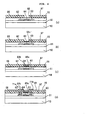
- Figs. 1 (a) and 1 (b) are drawings showing a TFT structure of the present invention.
- Fig. 1(a) shows a structure of a bottom gate type TFT
- Fig. 1(b) shows a structure of a top gate type TFT.
- an insulating polymer film 11 is provided on a substrate 10 such as insulating glass and ceramics, and a gate wiring formed by a plurality of conductive layers 13a and 13b are buried in a trench 12 formed in the insulating polymer film 11.
- the insulating polymer film 11 that can be employed in the present invention may be constituted of any one of insulating polymer material and polymer composition.
- thermoplastic resin or thermosetting resin such as polyacrylate, polystyrene, polyacrylate styrene, polyester, epoxy resin, polycarbonate resin, polyamide resin and the like.
- the polymer material that can be used as the insulating polymer film 11 in the present invention can be made of either photosensitive resin composition or photosensitive resin, that is, polymer or polymer composition that can be used as so-called photoresist, which is obtained by mixing or chemically combining photosensitve components with acrylic polymer, acrylic-styrene.polymer or epoxy polymer.
- photosensitive resin composition it is possible to enumerate: positive photoresist obtained by mixing quinone-diazo derivative to acrylic resin and phenolnovolac resin; positive or negative photoresist of so-called chemical amplification type obtained by mixing optical acid generator to acrylic resin, one of acrylic-styrene copolymer and acrylic-hydroxy styrene copolymer, and acrylic-alkoxy styrene copolymer; negative photoresist obtained by mixing acrylic resin with acrylate (methacrylate) having ethylene non-saturated bond, the negative photoresist enabling photo-polymerization by diazo compound; and epoxy photoresist obtained by mixing cation polymerization initiator to epoxy resin.
- positive photoresist obtained by mixing quinone-diazo derivative to acrylic resin and phenolnovolac resin
- positive or negative photoresist of so-called chemical amplification type obtained by mixing optical acid generator to acrylic resin, one of acrylic-styrene copolymer and acrylic-
- the photosenstive resin composition is not limited to the foregoing polymer or the foregoing photoresist, and any polymer or polymer composition can be used as long as the polymer or polymer composition is capable of forming the trench 12 by use of an appropriate patterning process for the polymer material.
- a thickness of the insulating polymer film 11 shown in Fig. 1(a) can be set in a range of 1 micrometer to 15 micrometers taking an electrical property such as an insulating property into consideration.
- the thickness of the insulating polymer film 11 should be set in a range of 2 micrometers to 10 micrometers in consideration for easiness of formation of the trench 12, more preferably in a range of 2 micrometers to 5 micrometers to particularly achieve a high definition and a large screen in the present invention.
- the gate wiring is formed by laminating the conductive layers 13a and 13b.
- the conductive layer 13a is a seed layer made of a metal such as Ni, which is formed by an electroless plating method.
- the conductive layer 13b is formed by an electroplating method and is formed so as to contain material for making resistivity of the gate wiring low.
- the conductive layer 13b is formed by a metal with low resistivity such as Al, Cu and Ag. Moreover, from the viewpoint of stability of the conductive layer 13b in the present invention, the conductive layer 13b should be formed by Al or Cu.
- a thickness of the gate wiring shown in Fig. 1(a) should be set to the same level as that of the insulating polymer film 11, and the thickness of the gate wiring can be set in a range of 1 micrometer to 15 micrometers depending on the requirement of the application. Moreover, in the present invention, the thickness of the gate wiring should be set in a range of 1 micrometer to 10 micrometers from the viewpoint of the high definition and the large screen of the display device and also from the viewpoint of reproducibility and stability of photolithography in manufacturing the insulating polymer film 11.
- the thickness of the gate wiring should be further preferably set in a range of 2 micrometers to 5 micrometers from the viewpoint of keeping a balance between the high definition and the large screen of the display device and easiness of the manufacturing processes including the process for forming the insulating polymer film 11.
- the insulating polymer film 11 and a top end of the gate wiring should be formed in a self-alignment with each other so that the TFT adjacent to the gate wiring is not adversely affected electrically.
- An insulating film 14 is deposited on the insulating polymer film 11 and on the top end of the gate wiring.
- Layers such as the source electrode 15, the drain electrode 16 and an active layer 17 made of material such as P* a-Si and N + a-Si are deposited on the insulating film 14.
- the layers are then patterned, and the respective electrodes are formed by metals or alloys such as Mo, MoW and MoTa to serve as constituent elements of the TFT.
- the gate wiring and the gate electrode, which is a constituent element of the TFT are formed so as to be adjacent to each other.
- the gate electrode and the gate wiring can be formed so as to be positionally shifted from each other in a horizontal direction on the insulating film 14.
- a size of the gate electrode can be set to any size required for the TFT structure.
- a passivation layer 18 made of an insulating material such as SiOx, SiNy and SiOxNy is formed on the constituent elements of the TFT such as the source electrode 15, the drain electrode 16 and the active layer, that is, a semiconductor layer 17.
- the passivation layer 18 serves to secure operations of the constituent elements of the TFT.
- Contact holes 20a and 20b are formed in the passivation layer 18, and a contact electrode 21a and a signal wiring 21b are connected to the source electrode 15 through the contact hole 20a and the drain electrode 16 through the contact hole 20b, respectively.
- Fig. 1(b) shows an embodiment in which the TFT structure of the present invention is applied to the top gate type TFT.
- the TFT shown in Fig. 1(b) is constituted in such a manner that an insulating layer 22 is formed on the insulating substrate 10, and a source electrode 23, a drain electrode 24, and an active layer 25 are formed on the insulating layer 22, thus constituting the TFT structure.
- An insulating film 26 made of insulating material such as SiOx, SiNy and SiOxNy is deposited on the constituent elements of the TFT such as the source electrode 23, the drain electrode 24 and the active layer 25 by use of an appropriate method such as a CVD method.
- the insulating layer 22 is optionally used from the viewpoint of characteristics and cost of the TFT.
- An insulating polymer film 27 containing the polymer material is formed on the insulating film 26, and a gate wiring 29 is buried and formed in a trench 28 formed in the insulating polymer film 27.
- the gate electrode is formed so as to be adjacent to the gate wiring 29 in the embodiment shown in Fig. 1(b).
- the gate electrode and the gate wiring 29 need not to be formed particularly so as to be adjacent to each other and can be formed so as to be apart from each other in the horizontal direction if necessary.
- the gate wiring shown in Fig. 1(b) is also constituted by the plurality of layers such as the seed layer formed by the electroless plating method and the conductive layer formed by the electroplating method. Note that, in the present invention, the gate wiring needs not to be a two-layer structure and can be formed with two or more layers if necessary.
- a passivation film 31 is deposited on the insulating polymer film 27, and a contact electrode 32a and a signal wiring 32b are connected to the source electrode 23 and the drain electrode 24 respectively, both through the passivation film 31, the insulating polymer film 27, and the insulating film 26.
- the same materials arid constitutions as those of each of the layers described in Fig. 1(a) can be employed for each of the films described in Fig. 1(b).
- Figs. 2(a) and 2(b) are drawings for explaining in detail operations of the conventional TFT structure and the TFT structure of the present invention.
- Fig. 2(a) shows the gate wiring of the conventional TFT structure
- Fig. 2(b) shows the gate wiring of the TFT structure of the present invention.
- a horizontal planar area of the conventional gate wiring 35 is inevitably expanded due to a film growth rate seen in a film growth method such as sputtering.
- the gate wiring 35 is constituted in the trench formed in the insulating polymer film 36 with a high aspect ratio while being self-aligned with the insulating film.
- the aspect ratio, or the ratio of the height (h) to the width (w), in the present invention is defined as the following equation, in which a height (h) is divided by a width (w).
- the constitution of the gate electrode 35 of the present invention enables the thickness of the gate electrode 35 to be increased while maintaining its characteristics. Accordingly, it is possible to make the cross sectional area of the gate electrode 35 larger and obtain desired characteristics such as a large screen and a high definition of the display device without causing the problem of the signal delay.
- the aspect ratio (As) of the gate electrode 35 in the present invention should be set in a range from 0.3 to 3 when the thickness of the gate electrode 35 ranges from 2 micrometers to 15 micrometers, to sufficiently achieve the object of the present invention that is a large screen and a high definition of the display device while giving the gate electrode a larger cross sectional area than that of the conventional gate electrode.
- the aspect ratio (As) of the gate electrode 35 should be especially set in a range from 0.4 to 3 when the thickness of the gate electrode 35 ranges from 2 micrometers to 15 micrometers.
- Figs. 3(a) to 3(f) show manufacturing steps of the method of manufacturing the TFT of the present invention.
- the insulating substrate 10 such as glass and ceramics, which has been subjected to a surface treatment if necessary, is prepared.
- the substrate 10 is first treated with a silane coupling agent, namely an aminosilane coupling agent, thus forming a Pd-containing catalyst layer 41 for performing electroless plating.
- the catalyst layer 41 can be formed in such a manner that, for example, the substrate 10 is immersed in a commercially available catalyst aqueous solution containing either Pd ions or Pd colloid, and metals are then separated out by reduction of the Pd ions according to need.
- an insulating polymer film 42 containing polymer is formed on the catalyst layer 41 by use of an appropriate coating method such as a spin coating method, for example.
- the polymer that can be used here is one of thermoplastic resin and thermosetting resin or photoresist as described in Fig. 1.
- the buried gate wiring can be formed without adding steps of exposure and development, by using one of the photosensitive resin and the photosensitive resin composition as the foregoing polymer material.
- Fig. 3(d) exposure and development are performed for the insulating polymer film 42 made of photoresist by using an appropriate photomask, thus forming a trench 43 for forming the gate wiring.
- the Pd catalyst is exposed at the bottom of the trench 43, and it is possible to selectively form a seed layer by use of the electroless plating method.
- the trench 43 can be formed by use of a method such as a screen printing method, not by use of the exposure and development processes.
- a method such as a screen printing method
- the screen printing method it is also possible to reduce the number of the processes irrespective of whether the insulating polymer film 42 used being one of the photosensitive resin and the photosensitive resin component or being one of the thermoplastic resin and the thermosetting resin.
- a step for forming a seed layer 44a in the trench 43 by the electroless plating in the present invention is shown in Fig. 3(e).
- conductive material for forming the seed layer 44a to function as a conductive layer any known metal can be employed. In the present invention, however, it is preferable to form the seed layer 44a using nickel (Ni) by the electroless plating method.
- Ni nickel
- adherability of the seed layer 44a to the substrate 10 made of a metal such as Cu, which is formed relatively thick and to be described later, can be enhanced. It is therefore possible to reduce disadvantages occurring due to detachment of the gate wiring from the substrate 10 as well as warping of the glass substrate, caused by an increase in in-film stress accompanied with the thickening of the insulating polymer film 42.
- the above described seed layer 44a can be formed by the electroless plating method by using, for example, a nickel sulfate aqueous solution containing hypophosphorous acid. Any known additives other than nickel sulfate may be added to the aqueous solution for forming the seed layer 44a.
- a thickness of the seed layer 44a shown in Fig. 3(e) is not particularly limited in the present invention, and the seed layer 44a can be formed to have any thickness as long as no disadvantages, such as the detachment of the gate wiring and the warping of the substrate caused by the formation of the seed layer 44a, occur.
- the electroless plating method for forming the seed layer 44a any known techniques may be employed.
- a conductive layer 44b formed by a metal with low resistivity such as Al, Cu, and Ag is deposited by the electroplating method, and the gate wiring is formed.
- the conductive layer 44b is formed by a metal such as copper (Cu) by applying the electroplating method
- the substrate 10 on which the structure shown in Fig. 3(e) is formed is immersed in a copper sulfate (CuSO 4 ) aqueous solution. Thereafter, by allowing current to flow therethrough, a deposition amount of Cu being separated out is controlled by a product of a current amount and duration according to the Faraday's law.
- CuSO 4 copper sulfate
- a gate wiring 45 can be formed in a self-alignment as described above is estimated as follows. Specifically, since the trench 43 is formed in the insulating polymer film 42 in the present invention, when the seed layer 44a is formed in the step shown in Fig. 3(e), the Pd catalyst adheres not only to the bottom but also to the walls of the trench 43 to some degree. Therefore, Cu can be well deposited from the bottom of the trench 43 not only upward along the walls of the trench 43, but also toward the center of the trench 43 from the walls thereof.
- the self-alignment of the gate wiring can be improved by depositing the gate wiring to a height where the gate wiring protrudes from the trench 43 and by applying a surface treatment such as polishing and etching thereafter.
- the gate electrode and the gate wiring can be formed so as to be adjacent to each other, or alternatively apart from each other, depending on requirements for the TFT structure.
- Ni is particularly used as the seed layer 44a
- Cu is used as the conductive layer 44b, whereby low resistivity in the TFT including a thick film wiring can be achieved without creating the occurrence of the disadvantage caused by the in-film stress, while satisfying the demand for the large screen and the high definition of the display device.
- the insulating polymer film 42 is used and a degree of unification of the gate wiring and the substrate 10 is enhanced by the seed layer 44a, a difference between the in-film stress and an expansion rate can be more absorbed compared to a case where SiO 2 is used as the insulating film.
- a TFT with a higher reliability can be provided.
- Figs. 4(a) to 4(d) are drawings showing manufacturing steps for forming the constituent elements of the TFT of the present invention subsequent to those shown in Figs. 3(a) to 3(f).
- an insulating film 47 made of an insulating layer such as SiOx, SiNy, and SiOxNy is deposited on the insulating polymer film 42, in which the gate wiring and the gate electrode are formed, by use of an appropriate method such as the CVD method, as shown in Fig. 4(a).
- an appropriate method such as the CVD method
- a source electrode 48, a drain electrode 49 and an active layer 50 are deposited on the gate insulating film 47 by any known methods including deposition, patterning, and ion-injection.
- These electrodes are constituted so as to contain an appropriate metal or alloy, which has been subjected to deposition or patterning, such as Mo, MoTa, MoW and Al.
- a passivation layer 51 formed by an insulating layer such as SiOx, SiNx and SiOxNy is deposited, and contact holes are formed in the passivation layer 51 by use of an appropriate patterning process.
- a contact electrode 52a and a signal wiring 52b are formed in the respective contact holes, thus completing the TFT structure of the present invention shown in Fig. 4(d).
- the TFT structure of the present invention has a constitution that the gate wiring is buried. Therefore, according to the present invention, an unnecessary difference in level is not created upon forming the TFT structure, and hence a reliability of the TFT can be enhanced.
- Figs. 5(a) to 5(e) are manufacturing steps showing another embodiment of a method of manufacturing a TFT structure when the TFT structure of the present invention is applied to a top gate type TFT.
- the top gate type TFT structure shown in Figs. 5(a) to 5(e) is formed according to the method of the present invention, first, the substrate 10 that has been subjected to a proper surface treatment is used as shown in Fig. 5(a). Then, an insulating layer 61 formed by a material such as SiOx, SiNy, and SiOxNy is deposited on the substrate 10 by use of an appropriate method such as the CVD method as shown in Fig. 5(b).
- a source electrode 62, a drain electrode 63 and an active layer 64 are deposited and patterned by use of the same process as described in Fig. 4(b).
- an insulating film 65 is deposited by a method such as the CVD method. After the deposition of the insulating film 65, a Pd catalyst 66 is allowed to adhere to the surface of the insulating film 65 in the same manner as that described in Fig. 3. An insulating polymer film 67 used in the present invention is then formed on the insulating film 65.
- the above-described manufacturing steps can be performed by use of the same methods as those described in Fig. 3.
- a trench 68 is formed in the insulating polymer film 67 deposited as shown in Fig. 5(d).
- a seed layer 69a is then formed by use of the electroless plating method as shown in Fig. 6(b), and a conductive layer 69b is deposited on the seed layer 69a by use of the electroplating method as shown in Fig. 6(c).
- a passivation layer 70 is formed on the entire surface of the resultant structure, and a contact electrode 71a and a signal wiring 71b are formed in the same manner as those described above, as shown in Fig. 6(d), thus completing the top gate type TFT.
- Figs. 7(a) to 7(e) are drawings showing still another embodiment of the method of manufacturing the TFT structure of the present invention.
- the substrate 10 that has been subjected to a surface treatment according to necessity is used as shown in Fig. 7(a), and an insulating polymer film 80 is formed on the substrate 10 as shown in Fig. 7(b).
- a trench 81 is formed by use of the same method as that described in Fig. 3.
- a water repellent layer 82 is transferred or formed by treating the insulating polymer film 80 and the substrate 10 with fluid dispersion obtained by dispersing silicone particles.
- the resultant structure shown in Fig. 7(d), in which the insulating polymer film 80 and the water repellent layer 82 are formed on the substrate 10, is immersed in a Pd catalyst aqueous solution, and a treatment with the Pd catalyst is performed for this resultant structure.
- Pd or Pd colloid adheres to the portion where the water repellent layer 82 is not formed, and the Pd or Pd colloid does not adhere to the portion where the water repellent layer 82 is formed. Therefore, as shown in Fig. 7(e), the seed layer 84a can be well formed by use of the electroless plating method.
- a conductive layer made of a metal with low resistivity such as Cu is deposited by the electroplating method, thus forming the gate wiring.
- the transfer of the water repellent layer 82 can be performed before the formation of the trench 81 shown Fig. 7(c).
- silicone-containing polymeric substance containing silicone segments can be used as the polymer.
- the silicon-containing polymeric substance containing silicone segments, mixed with the above-described polymers, can be used as the polymer. In this case, too, the silicone segments are exposed on the surface of the insulating polymer film 80.
- the silicone-containing polymeric substance When the above-described silicone-containing polymeric substance is used, a water repellent effect obtained by transferring the water repellent layer 82 by use of another step can also be obtained, and it is possible to selectively adhere the Pd catalyst. Furthermore, the polymer containing the foregoing silicone segments or the polymer composition can be formed as photosensitive resin or photosensitive resin composition.
- Figs. 8(a) and 8(b) and Fig. 9 are drawings showing the embodiment of the TFT structure in which the treatment is performed for the foregoing insulating polymer film of a bottom gate type TFT structure.
- a surface of an insulating polymer film 90 is subjected to a surface roughing treatment by use of, for example, a proper photolithography process, and a reflection film 90a is formed on the surface of the insulating polymer film 90 that has been subjected to the surface roughing treatment.
- the TFT structure is constituted so as to make a visual field angle wider.
- a reflection film made of any known material and constitution formed by, for example, the CVD process using various materials, can be used.
- the reflection film 90a can be formed as one layer structure, or a multilayered structure composed of dielectric.
- an insulating film 91 for flattening the entire surface of the resultant structure is formed on the surface that has been subjected to the surface roughing treatment, thus achieving a structure with no adverse influences on the constituent elements of the TFT.
- the same material as that constituting the insulating polymer film 90 can be used, or alternatively the insulating film 91 can be constituted by laminating material having different refractive index so as to create a scattering effect.
- Fig. 8(b) shows still another embodiment of the TFT structure of the present invention.
- a slope 90b is formed on the insulating polymer film 90, so as to form a prism.
- a polymer layer 92 having a still different refractive index is laminated on the insulating polymer film 90, thus constituting the prism. Accordingly, it is possible to achieve an enhanced visual field angle and high luminance even when the TFT structure having the structure shown in Fig. 8(b) is used.
- a Fresnel lens 90c is formed on the surface of the insulating polymer film 90, and another insulating material 93 having a further different refractive index is formed to create a flat surface on the Fresnel lens 90c, thus controlling a directivity of a beam of light.
- a polymer material can be used as the insulating material 93 similarly in the cases of the insulating films 91 and 92, dielectric other than polymer can also be used if necessary.
- the insulating polymer film 90 and a gate wiring 94 are formed so as to be self-aligned with each other in an adjacent portion in any case, and are formed not to have adverse influences on the constituent elements bf the TFT formed above.
- Fig. 10 is a graph in which a screen size (inch) and a resolution (PPI) in the embodiment of the TFT of the present invention shown in Fig. 2 are plotted.
- the lines (a), (b) , and ⁇ are for the gate wiring formed by the conventional method
- the line (d) is for the buried gate wiring of the present invention.
- the screen size becomes smaller due to the signal delay caused by an increase of resistivity as the gate wiring becomes thinner in an attempt to enhance the resolution.
- the TFT structure constituted by adopting the constitution of the buried gate wiring according to the present invention since the cross sectional area of the gate wiring can be increased as shown in Fig. 10(d) and the problem of the floating capacitance does not occur, it is possible to provide a screen size of about 25 inches while maintaining a high definition resolution of 400PPI. This tendency is apparent when compared with the case of the lower resolution, and it is indicated that the display device using the TFT structure adopting the gate wiring of the present invention can achieve a larger screen compared with that of the conventional display device.
- Fig. 11 is a perspective view showing a display device in which a TFT array is constituted by use of the TFT structure of the present invention.
- the TFT array shown in Fig. 11 is constituted as the bottom gate type TFT, and the TFT array is constituted by including an insulating polymer film 101 formed on an insulating substrate 100 and an insulating film 102 deposited on the insulating polymer film 101.
- a source electrode 103, a drain electrode 104 and an active layer 105 are formed on the insulating film 102 after being patterned.
- a passivation film 106 covers these constituent elements of the TFT to protect them.
- a contact electrode 107 and a signal wiring 108 are connected to the source electrode 103 and the drain electrode 104, respectively, through contact holes penetrating through the passivation film 106, and the above described constituent elements are arranged in a form of an array.
- a gate wiring 110 is constituted by depositing a plurality of conductive layers inside a trench 109 formed in the insulating polymer film 101 by the method of the present invention, and is buried therein.
- the TFT structure of the present invention as shown in Fig. 11, it is possible to make the cross sectional area of the gate wiring 110 larger than that of the conventional gate wiring.
- the gate wiring 110 having the large cross sectional area is buried in the insulating polymer film 101, and the gate wiring 110 is tightly united with the insulating polymer film 101 by use of the electroless plating and the electroplating.
- Fig. 12 is a drawing showing a TFT array in the case where the TFT structure of the present invention is applied to the top gate type TFT.
- the gate wiring 110 is formed by being buried in a trench formed in the insulating polymer film 101. Accordingly, it is possible to increase the cross sectional area of the gate electrode without causing disadvantages such as disconnection of wirings formed thereon.
- the TFT structure of the present invention can be employed in any display devices using a so-called active matrix driving system in which the TFTs are arranged in a form of an array as described above.
- a liquid crystal display device and an electroluminessence device using an inorganic or organic activation material can be listed as examples.
- the present invention was described accompanied with the embodiments shown in the drawings, the present invention is not limited to the embodiments shown in the drawings, and any known material, constitution and dimension in various constituent factors such as a constitution, a material and a dimension, can be employed as long as these constituent factors demonstrate the effects of the present invention.
Applications Claiming Priority (3)
| Application Number | Priority Date | Filing Date | Title |
|---|---|---|---|
| JP2001042081 | 2001-02-19 | ||
| JP2001042081 | 2001-02-19 | ||
| PCT/JP2001/011110 WO2002067335A1 (fr) | 2001-02-19 | 2001-12-18 | Structure de transistor en couches minces, procede de fabrication d'une structure de transistor en couches minces, et dispositif d'affichage utilisant une structure de transistor en couches minces |
Publications (3)
| Publication Number | Publication Date |
|---|---|
| EP1369928A1 true EP1369928A1 (de) | 2003-12-10 |
| EP1369928A4 EP1369928A4 (de) | 2006-01-11 |
| EP1369928B1 EP1369928B1 (de) | 2010-01-27 |
Family
ID=18904430
Family Applications (1)
| Application Number | Title | Priority Date | Filing Date |
|---|---|---|---|
| EP01273779A Expired - Lifetime EP1369928B1 (de) | 2001-02-19 | 2001-12-18 | Verfahren zur herstellung einer dünnfilmtransistorstruktur |
Country Status (9)
| Country | Link |
|---|---|
| US (2) | US6952036B2 (de) |
| EP (1) | EP1369928B1 (de) |
| JP (1) | JP4022470B2 (de) |
| KR (1) | KR100650417B1 (de) |
| CN (1) | CN100459163C (de) |
| AT (1) | ATE456863T1 (de) |
| DE (1) | DE60141225D1 (de) |
| TW (1) | TW541705B (de) |
| WO (1) | WO2002067335A1 (de) |
Cited By (7)
| Publication number | Priority date | Publication date | Assignee | Title |
|---|---|---|---|---|
| WO2004093198A1 (en) * | 2003-04-11 | 2004-10-28 | Applied Materials, Inc. | Methods to form metal lines using selective electrochemical deposition |
| WO2004100281A1 (en) * | 2003-05-12 | 2004-11-18 | Cambridge University Technical Services Limited | Polymer transistor |
| EP1651018A1 (de) * | 2003-06-04 | 2006-04-26 | Tadahiro Ohmi | Substrat und prozess zu seiner herstellung |
| US7223641B2 (en) | 2004-03-26 | 2007-05-29 | Semiconductor Energy Laboratory Co., Ltd. | Semiconductor device, method for manufacturing the same, liquid crystal television and EL television |
| US7575965B2 (en) | 2003-12-02 | 2009-08-18 | Semiconductor Energy Laboratory Co., Ltd. | Method for forming large area display wiring by droplet discharge, and method for manufacturing electronic device and semiconductor device |
| EP2151876A1 (de) * | 2008-08-05 | 2010-02-10 | Nederlandse Organisatie voor toegepast- natuurwetenschappelijk onderzoek TNO | Elektrische Transportkomponente, Herstellungsverfahren dafür sowie elektro-optische Vorrichtung und opto-elektrische Vorrichtung |
| US7868957B2 (en) | 2003-12-02 | 2011-01-11 | Semiconductor Energy Laboratory Co., Ltd. | Thin film transistor, display device and liquid crystal display device and method for manufacturing the same |
Families Citing this family (34)
| Publication number | Priority date | Publication date | Assignee | Title |
|---|---|---|---|---|
| ATE456863T1 (de) | 2001-02-19 | 2010-02-15 | Ibm | Verfahren zur herstellung einer dünnfilmtransistorstruktur |
| TWI253174B (en) * | 2003-05-09 | 2006-04-11 | Au Optronics Corp | Ion sensitive field effect transistor and fabrication method of the same |
| JP4712361B2 (ja) * | 2003-12-02 | 2011-06-29 | 株式会社半導体エネルギー研究所 | 薄膜トランジスタの作製方法 |
| JP4554344B2 (ja) * | 2003-12-02 | 2010-09-29 | 株式会社半導体エネルギー研究所 | 半導体装置の作製方法 |
| KR100636503B1 (ko) * | 2004-06-25 | 2006-10-18 | 삼성에스디아이 주식회사 | 발광 표시장치와 그의 제조방법 |
| JP2006030502A (ja) * | 2004-07-15 | 2006-02-02 | Sony Corp | 表示装置および表示装置の製造方法 |
| JP4628040B2 (ja) * | 2004-08-20 | 2011-02-09 | 株式会社半導体エネルギー研究所 | 半導体素子を備えた表示装置の製造方法 |
| CN100452325C (zh) * | 2005-03-22 | 2009-01-14 | 友达光电股份有限公司 | 一种薄膜晶体管与液晶显示器的制造方法 |
| WO2006134899A1 (ja) * | 2005-06-13 | 2006-12-21 | Tohoku University | 薄膜トランジスタ、配線板、及び電子装置の製造方法 |
| US20080217617A1 (en) * | 2005-07-05 | 2008-09-11 | Zeon Corporation | Thin Film Transistor, Wiring Board and Methods of Manufacturing the Same |
| US7397086B2 (en) * | 2005-12-23 | 2008-07-08 | Xerox Corporation | Top-gate thin-film transistor |
| JP2007203442A (ja) * | 2006-02-06 | 2007-08-16 | Univ Kanagawa | 金属被覆砥粒,金属被覆砥粒の製造方法,およびその金属被覆砥粒を使用した砥石 |
| WO2007142273A1 (ja) * | 2006-06-08 | 2007-12-13 | International Business Machines Corporation | 高熱伝導で柔軟なシート |
| TWI305682B (en) | 2006-08-14 | 2009-01-21 | Au Optronics Corp | Bottom substrate for liquid crystal display device and the method of making the same |
| JP2008103653A (ja) * | 2006-09-22 | 2008-05-01 | Tohoku Univ | 半導体装置及び半導体装置の製造方法 |
| KR101272489B1 (ko) * | 2006-10-03 | 2013-06-07 | 삼성디스플레이 주식회사 | 표시 기판, 이의 제조 방법 및 이를 구비하는 전기영동표시장치 |
| JP5329038B2 (ja) * | 2006-12-21 | 2013-10-30 | 宇部日東化成株式会社 | 半導体装置及び半導体装置の製造方法 |
| KR101418588B1 (ko) * | 2007-11-14 | 2014-07-16 | 삼성디스플레이 주식회사 | 표시 기판 및 이의 제조 방법 |
| GB2454740B (en) * | 2007-11-19 | 2011-12-21 | Hewlett Packard Development Co | Conductive interconnects |
| JP2010040897A (ja) * | 2008-08-07 | 2010-02-18 | Sony Corp | 有機薄膜トランジスタ、有機薄膜トランジスタの製造方法、および電子機器 |
| JP5533050B2 (ja) * | 2009-04-23 | 2014-06-25 | セイコーエプソン株式会社 | 半導体装置の製造方法、半導体装置、アクティブマトリクス装置、電気光学装置および電子機器 |
| US9099437B2 (en) * | 2011-03-08 | 2015-08-04 | Semiconductor Energy Laboratory Co., Ltd. | Semiconductor device |
| JP5891952B2 (ja) * | 2012-05-29 | 2016-03-23 | 株式会社ジャパンディスプレイ | 表示装置の製造方法 |
| KR20140061030A (ko) | 2012-11-13 | 2014-05-21 | 삼성디스플레이 주식회사 | 박막 트랜지스터 표시판 및 그 제조 방법 |
| KR20140064550A (ko) * | 2012-11-20 | 2014-05-28 | 삼성디스플레이 주식회사 | 박막 트랜지스터 표시판의 제조 방법 |
| CN105706222B (zh) * | 2013-11-21 | 2018-11-23 | 株式会社尼康 | 布线图案的制造方法和晶体管的制造方法 |
| TW201525064A (zh) * | 2013-12-16 | 2015-07-01 | Daxin Materials Corp | 感光樹脂組成物、感光樹脂及有機發光二極體顯示元件 |
| CN104795400B (zh) * | 2015-02-12 | 2018-10-30 | 合肥鑫晟光电科技有限公司 | 阵列基板制造方法、阵列基板和显示装置 |
| CN106128963B (zh) * | 2016-09-23 | 2019-07-23 | 京东方科技集团股份有限公司 | 薄膜晶体管及制备方法、阵列基板及制备方法、显示面板 |
| CN106876260B (zh) | 2017-03-03 | 2020-03-27 | 惠科股份有限公司 | 一种闸电极结构及其制造方法和显示装置 |
| CN107665896B (zh) * | 2017-10-27 | 2021-02-23 | 北京京东方显示技术有限公司 | 显示基板及其制作方法、显示面板和显示装置 |
| US11114475B2 (en) * | 2017-11-22 | 2021-09-07 | Shenzhen China Star Optoelectronics Semiconductor Display Technology Co., Ltd. | IPS thin-film transistor array substrate and manufacturing method thereof |
| CN109873037A (zh) * | 2019-03-20 | 2019-06-11 | 京东方科技集团股份有限公司 | 薄膜晶体管及其制备方法、显示装置 |
| CN113540127B (zh) * | 2021-07-19 | 2023-09-19 | 合肥鑫晟光电科技有限公司 | 一种背板、显示面板、显示装置及其制备方法 |
Family Cites Families (24)
| Publication number | Priority date | Publication date | Assignee | Title |
|---|---|---|---|---|
| JPS6418758U (de) * | 1987-07-25 | 1989-01-30 | ||
| DE69032773T2 (de) * | 1989-02-14 | 1999-05-27 | Seiko Epson Corp | Verfahren zur Herstellung einer Halbleitervorrichtung |
| JPH0651350A (ja) * | 1992-08-03 | 1994-02-25 | Alps Electric Co Ltd | 表示装置 |
| JPH06107881A (ja) * | 1992-09-30 | 1994-04-19 | Mitsubishi Rayon Co Ltd | 光拡散性メタクリル樹脂 |
| JPH06177126A (ja) * | 1992-12-01 | 1994-06-24 | Alps Electric Co Ltd | 薄膜積層体の形成方法 |
| JPH0823102A (ja) * | 1994-07-08 | 1996-01-23 | Matsushita Electric Ind Co Ltd | 電子部品及びその製造方法 |
| US5530293A (en) * | 1994-11-28 | 1996-06-25 | International Business Machines Corporation | Carbon-free hydrogen silsesquioxane with dielectric constant less than 3.2 annealed in hydrogen for integrated circuits |
| US5686329A (en) * | 1995-12-29 | 1997-11-11 | Taiwan Semiconductor Manufacturing Company, Ltd. | Method for forming a metal oxide semiconductor field effect transistor (MOSFET) having improved hot carrier immunity |
| GB2321336B (en) * | 1997-01-15 | 2001-07-25 | Univ Warwick | Gas-sensing semiconductor devices |
| JP3859181B2 (ja) | 1997-03-27 | 2006-12-20 | 東京応化工業株式会社 | 導電パターン形成方法 |
| US6121159A (en) * | 1997-06-19 | 2000-09-19 | Lsi Logic Corporation | Polymeric dielectric layers having low dielectric constants and improved adhesion to metal lines |
| JPH1146006A (ja) * | 1997-07-25 | 1999-02-16 | Canon Inc | 光起電力素子およびその製造方法 |
| JPH11232335A (ja) | 1998-02-13 | 1999-08-27 | Nec Corp | 注文管理装置 |
| JP3299167B2 (ja) | 1998-02-13 | 2002-07-08 | 日本板硝子株式会社 | 埋設電極付き基板の製造方法 |
| JPH11339672A (ja) * | 1998-05-29 | 1999-12-10 | Sony Corp | 画像表示装置の製造方法 |
| US6501098B2 (en) * | 1998-11-25 | 2002-12-31 | Semiconductor Energy Laboratory Co, Ltd. | Semiconductor device |
| US6225238B1 (en) * | 1999-06-07 | 2001-05-01 | Allied Signal Inc | Low dielectric constant polyorganosilicon coatings generated from polycarbosilanes |
| JP3272326B2 (ja) | 1999-06-14 | 2002-04-08 | 三協化学株式会社 | 2−ピリジルピリジン誘導体の製造方法 |
| KR20010046141A (ko) * | 1999-11-10 | 2001-06-05 | 구본준 | 박막 트랜지스터 및 배선 제조방법 |
| ATE456863T1 (de) | 2001-02-19 | 2010-02-15 | Ibm | Verfahren zur herstellung einer dünnfilmtransistorstruktur |
| US7045861B2 (en) * | 2002-03-26 | 2006-05-16 | Semiconductor Energy Laboratory Co., Ltd. | Light-emitting device, liquid-crystal display device and method for manufacturing same |
| US6825517B2 (en) * | 2002-08-28 | 2004-11-30 | Cova Technologies, Inc. | Ferroelectric transistor with enhanced data retention |
| TW200406829A (en) * | 2002-09-17 | 2004-05-01 | Adv Lcd Tech Dev Ct Co Ltd | Interconnect, interconnect forming method, thin film transistor, and display device |
| US6887776B2 (en) * | 2003-04-11 | 2005-05-03 | Applied Materials, Inc. | Methods to form metal lines using selective electrochemical deposition |
-
2001
- 2001-12-18 AT AT01273779T patent/ATE456863T1/de not_active IP Right Cessation
- 2001-12-18 CN CNB018227236A patent/CN100459163C/zh not_active Expired - Fee Related
- 2001-12-18 JP JP2002566560A patent/JP4022470B2/ja not_active Expired - Fee Related
- 2001-12-18 DE DE60141225T patent/DE60141225D1/de not_active Expired - Lifetime
- 2001-12-18 KR KR1020037010725A patent/KR100650417B1/ko not_active IP Right Cessation
- 2001-12-18 EP EP01273779A patent/EP1369928B1/de not_active Expired - Lifetime
- 2001-12-18 US US10/468,431 patent/US6952036B2/en not_active Expired - Fee Related
- 2001-12-18 WO PCT/JP2001/011110 patent/WO2002067335A1/ja active Application Filing
-
2002
- 2002-02-07 TW TW091102189A patent/TW541705B/zh not_active IP Right Cessation
-
2005
- 2005-06-27 US US11/167,637 patent/US7326600B2/en not_active Expired - Fee Related
Non-Patent Citations (2)
| Title |
|---|
| No further relevant documents disclosed * |
| See also references of WO02067335A1 * |
Cited By (15)
| Publication number | Priority date | Publication date | Assignee | Title |
|---|---|---|---|---|
| WO2004093198A1 (en) * | 2003-04-11 | 2004-10-28 | Applied Materials, Inc. | Methods to form metal lines using selective electrochemical deposition |
| US6887776B2 (en) | 2003-04-11 | 2005-05-03 | Applied Materials, Inc. | Methods to form metal lines using selective electrochemical deposition |
| WO2004100281A1 (en) * | 2003-05-12 | 2004-11-18 | Cambridge University Technical Services Limited | Polymer transistor |
| EP1651018A4 (de) * | 2003-06-04 | 2009-11-11 | Tadahiro Ohmi | Substrat und prozess zu seiner herstellung |
| EP1651018A1 (de) * | 2003-06-04 | 2006-04-26 | Tadahiro Ohmi | Substrat und prozess zu seiner herstellung |
| US7575965B2 (en) | 2003-12-02 | 2009-08-18 | Semiconductor Energy Laboratory Co., Ltd. | Method for forming large area display wiring by droplet discharge, and method for manufacturing electronic device and semiconductor device |
| US7868957B2 (en) | 2003-12-02 | 2011-01-11 | Semiconductor Energy Laboratory Co., Ltd. | Thin film transistor, display device and liquid crystal display device and method for manufacturing the same |
| US7897968B2 (en) | 2003-12-02 | 2011-03-01 | Semiconductor Energy Laboratory Co., Ltd. | Electronic device and semiconductor device and method for manufacturing the same |
| US8228453B2 (en) | 2003-12-02 | 2012-07-24 | Semiconductor Energy Laboratory Co., Ltd. | Thin film transistor, display device and liquid crystal display device and method for manufacturing the same |
| US8619219B2 (en) | 2003-12-02 | 2013-12-31 | Semiconductor Energy Laboratory Co., Ltd. | Thin film transistor, display device and liquid crystal display device and method for manufacturing the same |
| US7223641B2 (en) | 2004-03-26 | 2007-05-29 | Semiconductor Energy Laboratory Co., Ltd. | Semiconductor device, method for manufacturing the same, liquid crystal television and EL television |
| EP2151876A1 (de) * | 2008-08-05 | 2010-02-10 | Nederlandse Organisatie voor toegepast- natuurwetenschappelijk onderzoek TNO | Elektrische Transportkomponente, Herstellungsverfahren dafür sowie elektro-optische Vorrichtung und opto-elektrische Vorrichtung |
| WO2010016763A1 (en) * | 2008-08-05 | 2010-02-11 | Nederlandse Organisatie Voor Toegepast-Natuurwetenschappelijk Onderzoek Tno | Electric transport component, method of manufacturing the same, as well as electro-optical device and opto-electrical device |
| US8507899B2 (en) | 2008-08-05 | 2013-08-13 | Nederlandse Organisatie Voor Toegepast-Natuurwetenschappelijk Onderzoek Tno | Electric transport component, method of manufacturing the same, as well as electro-optical device and opto-electrical device |
| CN102144310B (zh) * | 2008-08-05 | 2013-08-28 | 荷兰应用科学研究会(Tno) | 电输送部件、制造该部件的方法以及电光器件和光电器件 |
Also Published As
| Publication number | Publication date |
|---|---|
| CN1489790A (zh) | 2004-04-14 |
| WO2002067335A1 (fr) | 2002-08-29 |
| EP1369928B1 (de) | 2010-01-27 |
| JP4022470B2 (ja) | 2007-12-19 |
| ATE456863T1 (de) | 2010-02-15 |
| KR20030077621A (ko) | 2003-10-01 |
| JPWO2002067335A1 (ja) | 2004-06-24 |
| US20040113161A1 (en) | 2004-06-17 |
| KR100650417B1 (ko) | 2006-11-28 |
| TW541705B (en) | 2003-07-11 |
| US20050250262A1 (en) | 2005-11-10 |
| CN100459163C (zh) | 2009-02-04 |
| EP1369928A4 (de) | 2006-01-11 |
| US7326600B2 (en) | 2008-02-05 |
| US6952036B2 (en) | 2005-10-04 |
| DE60141225D1 (de) | 2010-03-18 |
Similar Documents
| Publication | Publication Date | Title |
|---|---|---|
| EP1369928B1 (de) | Verfahren zur herstellung einer dünnfilmtransistorstruktur | |
| US8368856B2 (en) | Transflective liquid crystal display device and method of fabricating the same | |
| US7488983B2 (en) | Transflective liquid crystal display device and method of fabricating the same | |
| US8791459B2 (en) | Array substrate, manufacturing method of the same, and fabricating method of display device including the array substrate | |
| US7687330B2 (en) | TFT-LCD pixel structure and manufacturing method thereof | |
| US20070200984A1 (en) | Reflection type liquid crystal display device and method of manufacturing the same | |
| US7999262B2 (en) | Thin film transistor, method of fabricating the same, and method of fabricating liquid crystal display device having the same | |
| US7277138B2 (en) | Array substrate for LCD device having double-layered metal structure and manufacturing method thereof | |
| US7678619B2 (en) | Method of manufacturing a thin film transistor matrix substrate | |
| KR20080003706A (ko) | 액정표시장치의 기판 및 그 제조방법 | |
| CN101373736A (zh) | 互连、互连形成方法、薄膜晶体管及显示器 | |
| US7230668B2 (en) | Reflection type liquid crystal display device with a passivation layer directly on the pad electrode | |
| CN101013740A (zh) | 有机薄膜晶体管及其制造方法 | |
| US20050142704A1 (en) | Method for fabricating liquid crystal display device | |
| US6961101B2 (en) | Copper alloy, array substrate of liquid crystal display using the same and method of fabricating the same | |
| US7177003B2 (en) | LCD with gate and data lines formed of copper and an aluminum under-layer | |
| US20070264597A1 (en) | Method for manufacturing transflective liquid crystal display | |
| KR20050118537A (ko) | 액정표시장치용 기판 및 그 제조방법 | |
| US7932979B2 (en) | Method for fabricating a liquid crystal display device wherein the storage electrode is simultaneously formed with the active pattern | |
| KR20020031765A (ko) | 액정표시장치용 어레이 기판 및 그의 제조방법 | |
| KR100701657B1 (ko) | 액정표시소자 패널의 제조방법 | |
| US6398974B1 (en) | Method of forming an electrode for a thin film transistor | |
| KR20020031764A (ko) | 액정표시장치용 어레이패널 및 그의 제조방법 |
Legal Events
| Date | Code | Title | Description |
|---|---|---|---|
| PUAI | Public reference made under article 153(3) epc to a published international application that has entered the european phase |
Free format text: ORIGINAL CODE: 0009012 |
|
| 17P | Request for examination filed |
Effective date: 20030915 |
|
| AK | Designated contracting states |
Kind code of ref document: A1 Designated state(s): AT BE CH CY DE DK ES FI FR GB GR IE IT LI LU MC NL PT SE TR |
|
| AX | Request for extension of the european patent |
Extension state: AL LT LV MK RO SI |
|
| A4 | Supplementary search report drawn up and despatched |
Effective date: 20051130 |
|
| 17Q | First examination report despatched |
Effective date: 20060911 |
|
| RTI1 | Title (correction) |
Free format text: METHOD FOR MANUFACTURING A THIN-FILM TRANSISTOR STRUCTURE |
|
| GRAP | Despatch of communication of intention to grant a patent |
Free format text: ORIGINAL CODE: EPIDOSNIGR1 |
|
| GRAS | Grant fee paid |
Free format text: ORIGINAL CODE: EPIDOSNIGR3 |
|
| GRAA | (expected) grant |
Free format text: ORIGINAL CODE: 0009210 |
|
| AK | Designated contracting states |
Kind code of ref document: B1 Designated state(s): AT BE CH CY DE DK ES FI FR GB GR IE IT LI LU MC NL PT SE TR |
|
| REG | Reference to a national code |
Ref country code: GB Ref legal event code: FG4D |
|
| REG | Reference to a national code |
Ref country code: CH Ref legal event code: EP Ref country code: CH Ref legal event code: NV Representative=s name: IBM RESEARCH GMBH ZURICH RESEARCH LABORATORY INTEL |
|
| REG | Reference to a national code |
Ref country code: GB Ref legal event code: 746 Effective date: 20100202 |
|
| REG | Reference to a national code |
Ref country code: IE Ref legal event code: FG4D |
|
| REF | Corresponds to: |
Ref document number: 60141225 Country of ref document: DE Date of ref document: 20100318 Kind code of ref document: P |
|
| REG | Reference to a national code |
Ref country code: NL Ref legal event code: VDEP Effective date: 20100127 |
|
| PG25 | Lapsed in a contracting state [announced via postgrant information from national office to epo] |
Ref country code: AT Free format text: LAPSE BECAUSE OF FAILURE TO SUBMIT A TRANSLATION OF THE DESCRIPTION OR TO PAY THE FEE WITHIN THE PRESCRIBED TIME-LIMIT Effective date: 20100127 |
|
| PG25 | Lapsed in a contracting state [announced via postgrant information from national office to epo] |
Ref country code: PT Free format text: LAPSE BECAUSE OF FAILURE TO SUBMIT A TRANSLATION OF THE DESCRIPTION OR TO PAY THE FEE WITHIN THE PRESCRIBED TIME-LIMIT Effective date: 20100527 Ref country code: NL Free format text: LAPSE BECAUSE OF FAILURE TO SUBMIT A TRANSLATION OF THE DESCRIPTION OR TO PAY THE FEE WITHIN THE PRESCRIBED TIME-LIMIT Effective date: 20100127 Ref country code: ES Free format text: LAPSE BECAUSE OF FAILURE TO SUBMIT A TRANSLATION OF THE DESCRIPTION OR TO PAY THE FEE WITHIN THE PRESCRIBED TIME-LIMIT Effective date: 20100508 |
|
| PG25 | Lapsed in a contracting state [announced via postgrant information from national office to epo] |
Ref country code: FI Free format text: LAPSE BECAUSE OF FAILURE TO SUBMIT A TRANSLATION OF THE DESCRIPTION OR TO PAY THE FEE WITHIN THE PRESCRIBED TIME-LIMIT Effective date: 20100127 |
|
| PG25 | Lapsed in a contracting state [announced via postgrant information from national office to epo] |
Ref country code: SE Free format text: LAPSE BECAUSE OF FAILURE TO SUBMIT A TRANSLATION OF THE DESCRIPTION OR TO PAY THE FEE WITHIN THE PRESCRIBED TIME-LIMIT Effective date: 20100127 Ref country code: BE Free format text: LAPSE BECAUSE OF FAILURE TO SUBMIT A TRANSLATION OF THE DESCRIPTION OR TO PAY THE FEE WITHIN THE PRESCRIBED TIME-LIMIT Effective date: 20100127 Ref country code: CY Free format text: LAPSE BECAUSE OF FAILURE TO SUBMIT A TRANSLATION OF THE DESCRIPTION OR TO PAY THE FEE WITHIN THE PRESCRIBED TIME-LIMIT Effective date: 20100127 Ref country code: GR Free format text: LAPSE BECAUSE OF FAILURE TO SUBMIT A TRANSLATION OF THE DESCRIPTION OR TO PAY THE FEE WITHIN THE PRESCRIBED TIME-LIMIT Effective date: 20100428 |
|
| PLBE | No opposition filed within time limit |
Free format text: ORIGINAL CODE: 0009261 |
|
| STAA | Information on the status of an ep patent application or granted ep patent |
Free format text: STATUS: NO OPPOSITION FILED WITHIN TIME LIMIT |
|
| 26N | No opposition filed |
Effective date: 20101028 |
|
| PG25 | Lapsed in a contracting state [announced via postgrant information from national office to epo] |
Ref country code: DK Free format text: LAPSE BECAUSE OF FAILURE TO SUBMIT A TRANSLATION OF THE DESCRIPTION OR TO PAY THE FEE WITHIN THE PRESCRIBED TIME-LIMIT Effective date: 20100127 |
|
| PG25 | Lapsed in a contracting state [announced via postgrant information from national office to epo] |
Ref country code: IT Free format text: LAPSE BECAUSE OF FAILURE TO SUBMIT A TRANSLATION OF THE DESCRIPTION OR TO PAY THE FEE WITHIN THE PRESCRIBED TIME-LIMIT Effective date: 20100127 |
|
| PG25 | Lapsed in a contracting state [announced via postgrant information from national office to epo] |
Ref country code: MC Free format text: LAPSE BECAUSE OF NON-PAYMENT OF DUE FEES Effective date: 20101231 |
|
| REG | Reference to a national code |
Ref country code: CH Ref legal event code: PL |
|
| PG25 | Lapsed in a contracting state [announced via postgrant information from national office to epo] |
Ref country code: LI Free format text: LAPSE BECAUSE OF NON-PAYMENT OF DUE FEES Effective date: 20101231 Ref country code: CH Free format text: LAPSE BECAUSE OF NON-PAYMENT OF DUE FEES Effective date: 20101231 Ref country code: IE Free format text: LAPSE BECAUSE OF NON-PAYMENT OF DUE FEES Effective date: 20101218 |
|
| PG25 | Lapsed in a contracting state [announced via postgrant information from national office to epo] |
Ref country code: LU Free format text: LAPSE BECAUSE OF NON-PAYMENT OF DUE FEES Effective date: 20101218 |
|
| PG25 | Lapsed in a contracting state [announced via postgrant information from national office to epo] |
Ref country code: TR Free format text: LAPSE BECAUSE OF FAILURE TO SUBMIT A TRANSLATION OF THE DESCRIPTION OR TO PAY THE FEE WITHIN THE PRESCRIBED TIME-LIMIT Effective date: 20100127 |
|
| PGFP | Annual fee paid to national office [announced via postgrant information from national office to epo] |
Ref country code: FR Payment date: 20130110 Year of fee payment: 12 |
|
| REG | Reference to a national code |
Ref country code: FR Ref legal event code: ST Effective date: 20140829 |
|
| PG25 | Lapsed in a contracting state [announced via postgrant information from national office to epo] |
Ref country code: FR Free format text: LAPSE BECAUSE OF NON-PAYMENT OF DUE FEES Effective date: 20131231 |
|
| PGFP | Annual fee paid to national office [announced via postgrant information from national office to epo] |
Ref country code: DE Payment date: 20181116 Year of fee payment: 18 |
|
| PGFP | Annual fee paid to national office [announced via postgrant information from national office to epo] |
Ref country code: GB Payment date: 20181228 Year of fee payment: 18 |
|
| REG | Reference to a national code |
Ref country code: DE Ref legal event code: R119 Ref document number: 60141225 Country of ref document: DE |
|
| GBPC | Gb: european patent ceased through non-payment of renewal fee |
Effective date: 20191218 |
|
| PG25 | Lapsed in a contracting state [announced via postgrant information from national office to epo] |
Ref country code: DE Free format text: LAPSE BECAUSE OF NON-PAYMENT OF DUE FEES Effective date: 20200701 Ref country code: GB Free format text: LAPSE BECAUSE OF NON-PAYMENT OF DUE FEES Effective date: 20191218 |