EP1365214A1 - Sensor mit einem, aus einem Array von Dachkantenspiegel und -prismen, bestehenden Massstab, und Apparatus mit einem derartigen Sensor - Google Patents
Sensor mit einem, aus einem Array von Dachkantenspiegel und -prismen, bestehenden Massstab, und Apparatus mit einem derartigen Sensor Download PDFInfo
- Publication number
- EP1365214A1 EP1365214A1 EP03253116A EP03253116A EP1365214A1 EP 1365214 A1 EP1365214 A1 EP 1365214A1 EP 03253116 A EP03253116 A EP 03253116A EP 03253116 A EP03253116 A EP 03253116A EP 1365214 A1 EP1365214 A1 EP 1365214A1
- Authority
- EP
- European Patent Office
- Prior art keywords
- light
- reflecting
- scale
- array
- light source
- Prior art date
- Legal status (The legal status is an assumption and is not a legal conclusion. Google has not performed a legal analysis and makes no representation as to the accuracy of the status listed.)
- Withdrawn
Links
- 230000003287 optical effect Effects 0.000 claims description 81
- 238000006073 displacement reaction Methods 0.000 claims description 79
- 238000006243 chemical reaction Methods 0.000 claims description 16
- 230000009471 action Effects 0.000 claims description 8
- 238000009826 distribution Methods 0.000 claims description 5
- 230000010354 integration Effects 0.000 claims description 4
- 239000003550 marker Substances 0.000 claims description 4
- 230000003595 spectral effect Effects 0.000 claims description 4
- 239000012141 concentrate Substances 0.000 claims 1
- 239000002184 metal Substances 0.000 claims 1
- 238000012856 packing Methods 0.000 claims 1
- 230000001965 increasing effect Effects 0.000 abstract description 14
- 238000010276 construction Methods 0.000 description 45
- 230000014509 gene expression Effects 0.000 description 30
- 239000000758 substrate Substances 0.000 description 14
- 239000004065 semiconductor Substances 0.000 description 11
- 238000001514 detection method Methods 0.000 description 9
- 238000012545 processing Methods 0.000 description 9
- 230000009467 reduction Effects 0.000 description 9
- 239000010408 film Substances 0.000 description 6
- 230000005540 biological transmission Effects 0.000 description 5
- 238000005253 cladding Methods 0.000 description 5
- ORQBXQOJMQIAOY-UHFFFAOYSA-N nobelium Chemical compound [No] ORQBXQOJMQIAOY-UHFFFAOYSA-N 0.000 description 5
- XAGFODPZIPBFFR-UHFFFAOYSA-N aluminium Chemical compound [Al] XAGFODPZIPBFFR-UHFFFAOYSA-N 0.000 description 4
- 229910052782 aluminium Inorganic materials 0.000 description 4
- 230000000694 effects Effects 0.000 description 4
- 238000001704 evaporation Methods 0.000 description 4
- 230000002349 favourable effect Effects 0.000 description 4
- 238000002474 experimental method Methods 0.000 description 3
- 230000004907 flux Effects 0.000 description 3
- 239000011521 glass Substances 0.000 description 3
- 238000002347 injection Methods 0.000 description 3
- 239000007924 injection Substances 0.000 description 3
- 239000000463 material Substances 0.000 description 3
- 238000000034 method Methods 0.000 description 3
- 230000035945 sensitivity Effects 0.000 description 3
- XUIMIQQOPSSXEZ-UHFFFAOYSA-N Silicon Chemical compound [Si] XUIMIQQOPSSXEZ-UHFFFAOYSA-N 0.000 description 2
- 230000003247 decreasing effect Effects 0.000 description 2
- 238000005530 etching Methods 0.000 description 2
- 230000008020 evaporation Effects 0.000 description 2
- 238000004519 manufacturing process Methods 0.000 description 2
- 238000005259 measurement Methods 0.000 description 2
- 230000004048 modification Effects 0.000 description 2
- 238000012986 modification Methods 0.000 description 2
- 230000000737 periodic effect Effects 0.000 description 2
- 229920003229 poly(methyl methacrylate) Polymers 0.000 description 2
- 239000004417 polycarbonate Substances 0.000 description 2
- 229920000515 polycarbonate Polymers 0.000 description 2
- 239000004926 polymethyl methacrylate Substances 0.000 description 2
- 229910052710 silicon Inorganic materials 0.000 description 2
- 239000010703 silicon Substances 0.000 description 2
- 239000010409 thin film Substances 0.000 description 2
- VYZAMTAEIAYCRO-UHFFFAOYSA-N Chromium Chemical compound [Cr] VYZAMTAEIAYCRO-UHFFFAOYSA-N 0.000 description 1
- 239000004593 Epoxy Substances 0.000 description 1
- 230000003321 amplification Effects 0.000 description 1
- 230000008859 change Effects 0.000 description 1
- 229910052804 chromium Inorganic materials 0.000 description 1
- 239000011651 chromium Substances 0.000 description 1
- 150000001875 compounds Chemical class 0.000 description 1
- 238000007796 conventional method Methods 0.000 description 1
- 239000013078 crystal Substances 0.000 description 1
- 238000010586 diagram Methods 0.000 description 1
- 230000002708 enhancing effect Effects 0.000 description 1
- 230000020169 heat generation Effects 0.000 description 1
- 229920006015 heat resistant resin Polymers 0.000 description 1
- 230000001678 irradiating effect Effects 0.000 description 1
- 238000004020 luminiscence type Methods 0.000 description 1
- JFNLZVQOOSMTJK-KNVOCYPGSA-N norbornene Chemical compound C1[C@@H]2CC[C@H]1C=C2 JFNLZVQOOSMTJK-KNVOCYPGSA-N 0.000 description 1
- 238000003199 nucleic acid amplification method Methods 0.000 description 1
- 230000002093 peripheral effect Effects 0.000 description 1
- 239000004033 plastic Substances 0.000 description 1
- 229920003023 plastic Polymers 0.000 description 1
- 230000008569 process Effects 0.000 description 1
- 239000011347 resin Substances 0.000 description 1
- 229920005989 resin Polymers 0.000 description 1
- 230000006641 stabilisation Effects 0.000 description 1
- 238000011105 stabilization Methods 0.000 description 1
- 230000000087 stabilizing effect Effects 0.000 description 1
Images


Classifications
-
- G—PHYSICS
- G01—MEASURING; TESTING
- G01D—MEASURING NOT SPECIALLY ADAPTED FOR A SPECIFIC VARIABLE; ARRANGEMENTS FOR MEASURING TWO OR MORE VARIABLES NOT COVERED IN A SINGLE OTHER SUBCLASS; TARIFF METERING APPARATUS; MEASURING OR TESTING NOT OTHERWISE PROVIDED FOR
- G01D5/00—Mechanical means for transferring the output of a sensing member; Means for converting the output of a sensing member to another variable where the form or nature of the sensing member does not constrain the means for converting; Transducers not specially adapted for a specific variable
- G01D5/26—Mechanical means for transferring the output of a sensing member; Means for converting the output of a sensing member to another variable where the form or nature of the sensing member does not constrain the means for converting; Transducers not specially adapted for a specific variable characterised by optical transfer means, i.e. using infrared, visible, or ultraviolet light
- G01D5/32—Mechanical means for transferring the output of a sensing member; Means for converting the output of a sensing member to another variable where the form or nature of the sensing member does not constrain the means for converting; Transducers not specially adapted for a specific variable characterised by optical transfer means, i.e. using infrared, visible, or ultraviolet light with attenuation or whole or partial obturation of beams of light
- G01D5/34—Mechanical means for transferring the output of a sensing member; Means for converting the output of a sensing member to another variable where the form or nature of the sensing member does not constrain the means for converting; Transducers not specially adapted for a specific variable characterised by optical transfer means, i.e. using infrared, visible, or ultraviolet light with attenuation or whole or partial obturation of beams of light the beams of light being detected by photocells
- G01D5/36—Forming the light into pulses
- G01D5/38—Forming the light into pulses by diffraction gratings
-
- G—PHYSICS
- G01—MEASURING; TESTING
- G01D—MEASURING NOT SPECIALLY ADAPTED FOR A SPECIFIC VARIABLE; ARRANGEMENTS FOR MEASURING TWO OR MORE VARIABLES NOT COVERED IN A SINGLE OTHER SUBCLASS; TARIFF METERING APPARATUS; MEASURING OR TESTING NOT OTHERWISE PROVIDED FOR
- G01D5/00—Mechanical means for transferring the output of a sensing member; Means for converting the output of a sensing member to another variable where the form or nature of the sensing member does not constrain the means for converting; Transducers not specially adapted for a specific variable
- G01D5/26—Mechanical means for transferring the output of a sensing member; Means for converting the output of a sensing member to another variable where the form or nature of the sensing member does not constrain the means for converting; Transducers not specially adapted for a specific variable characterised by optical transfer means, i.e. using infrared, visible, or ultraviolet light
- G01D5/32—Mechanical means for transferring the output of a sensing member; Means for converting the output of a sensing member to another variable where the form or nature of the sensing member does not constrain the means for converting; Transducers not specially adapted for a specific variable characterised by optical transfer means, i.e. using infrared, visible, or ultraviolet light with attenuation or whole or partial obturation of beams of light
- G01D5/34—Mechanical means for transferring the output of a sensing member; Means for converting the output of a sensing member to another variable where the form or nature of the sensing member does not constrain the means for converting; Transducers not specially adapted for a specific variable characterised by optical transfer means, i.e. using infrared, visible, or ultraviolet light with attenuation or whole or partial obturation of beams of light the beams of light being detected by photocells
- G01D5/347—Mechanical means for transferring the output of a sensing member; Means for converting the output of a sensing member to another variable where the form or nature of the sensing member does not constrain the means for converting; Transducers not specially adapted for a specific variable characterised by optical transfer means, i.e. using infrared, visible, or ultraviolet light with attenuation or whole or partial obturation of beams of light the beams of light being detected by photocells using displacement encoding scales
- G01D5/34707—Scales; Discs, e.g. fixation, fabrication, compensation
- G01D5/34715—Scale reading or illumination devices
Definitions
- the present invention relates to a displacement measuring apparatus, and in particular to a displacement measuring apparatus, such as a linear encoder or a rotary encoder, that detects displacement information, such as the moving amount, moving speed, and rotation speed, of a moving body using an optical scale.
- a displacement measuring apparatus such as a linear encoder or a rotary encoder, that detects displacement information, such as the moving amount, moving speed, and rotation speed, of a moving body using an optical scale.
- Such a displacement measuring apparatus is proposed in Japanese Patent Publication No. 60-23282, Japanese Utility Model Application Laid-Open No. 1-180615, and the like, for instance.
- FIGS. 26 and 27 are each a schematic drawing showing the main portion of an optical system of the displacement measuring apparatus proposed in Japanese Patent Publication No. 60-23282.
- reference numerals 103, 104, and 105 respectively denote a first scale, a second scale, and a third scale that each have a grating provided with light transmission portions and non-transmission portions at a constant pitch P 1 , P 2 , or P 3 . Also, these first to third scales are each opposedly arranged approximately parallel to a displacement detecting direction 106.
- Reference numeral 101 indicates a light source that radiates a light flux whose luminescence center wavelength is ⁇ m
- reference numeral 102 indicates a light-receiving element.
- the second scale 104, the third scale 105, the light source 101, and the light-receiving element 102 are integrally contained within a single case.
- the first scale 103 is provided for a moving body (not shown) and is capable of moving in the direction of an arrow 106.
- the light beam from the light source 101 is made incident on the second scale 104, is light-modulated by the second scale 104, and is made incident on the first scale 103. Then, the light beam is light-modulated by the first scale 103, is made incident on the third scale 105, is light-modulated by the third scale 105, and is made incident on the light-receiving element 102 to be detected.
- the space between the second scale 104 and the first scale 103 is referred to as " ⁇ "
- the space between the first scale 103 and the third scale 105 is referred to as "V”
- a natural number is referred to as "n”, as shown in the drawing.
- a geometrical real image concerning the grating of the first scale 103 and a diffraction optical real image concerning the grating of the first scale 103 are respectively formed by the light beam light-modulated by the second scale 104 and the first scale 103 at the position of the third scale 105 if Expressions (1) to (5) given below are satisfied.
- the geometrical real image and the diffraction optical real image will be hereinafter referred to as the "grating image”.
- the grating image becomes an image having a periodic contrast with a pitch P 3 that is the same as a grating pitch P 3 of the third scale 105.
- the grating image forming on the third scale 105 also moves.
- the intensity of light passing through the third scale 105 changes along with the movement of the grating image and a periodic displacement signal concerning movement information of the first scale 103 is obtained from the light-receiving element 102.
- the illustrated displacement measuring apparatus detects movement information of the first scale 103, which is a moving body in this example, using the displacement signal obtained from the light-receiving element 102.
- FIG. 27 is a schematic drawing showing the main portion of an optical system of another displacement measuring apparatus proposed in Japanese Patent Publication No. 60-23282 described above.
- the displacement measuring apparatus in this drawing differs from the displacement measuring apparatus shown in FIG. 26 in that a first scale 113 is of a reflection type and a second scale 116 doubles as a third scale, although there is used the same optical displacement detecting principle.
- a light beam from a light source 111 is irradiated onto the second scale 116 through a half mirror 117, a light-modulated light beam from the second scale 116 is made incident on the first scale 113, and reflected which is light light-modulated by the first scale 113 is made incident on the second scale 116. Then, the light-modulated light beam from the second scale 116 is detected by a light-receiving element 112 through the half mirror 117.
- the reflection-type displacement detecting system has more merits than the transmission-type displacement detecting system. For instance, the number of required scales is substantially reduced from three to two, as can be seen from FIG. 27.
- the reflection-type displacement detecting system is favorable in terms of miniaturization, in comparison with the transmission-type displacement detecting system.
- Expression (6) is a general expression that gives a substantial positional relation that is in particular optimum for the reflection-type construction.
- FIG. 28 is a schematic drawing showing the main portion of an optical system of the displacement measuring apparatus proposed in Japanese Utility Model Application Laid-Open No. 1-180615.
- reference numerals 123, 124, and 125 respectively denote a first scale, a second scale, and a third scale, numeral 121 a light source, and numeral 122 (122a, 122b) a light-receiving element.
- the first scale 123 is produced using a reflection-type scale and is provided for a moving body (not shown) so as to be movable in the direction of the arrow 126.
- the principle of the first scale 123 to detect displacement information is the same as that of the displacement measuring apparatus illustrated in FIG. 26.
- a light beam from the light source 121 is made incident on the second scale 124 in a diverging manner, is light-modulated by the second scale, and is made incident on the first scale 123.
- two reflected lights light-modulated by a displacement of the first scale 123 are detected by the light-receiving elements 122a and 122b through the third scales 125a and 125b provided adjacent to each other on approximately the same plane as the second scale 124.
- there are obtained displacement signals concerning movement information of the first scale 123 in the direction of the arrow 126 as is the case of the displacement measuring apparatus in FIG. 26.
- a metallic scale produced by forming many slit opening portions in a metallic substrate through etching
- a glass scale produced by forming many slit opening portions in a glass substrate through evaporation of Chromium thin film or Aluminum thin film or the like and etching, or the like.
- FIGS. 29 and 30 are each a schematic drawing showing the main portion of another optical system of the displacement measuring apparatus proposed in Japanese Utility Model Application Laid-Open No. 1-180615.
- FIG. 32 where a shortage of light intensity is compensated for using a lens
- FIGS. 33 and 34 where direct reflected light is used as a reflecting body and a distance between a reflecting body and a light source is further reduced, thereby avoiding the shortage of light intensity.
- the reflection-type displacement measuring apparatus shown in FIG. 27 there is used a half mirror, so that the size of the apparatus is increased as a whole and the loss of intensity of light from the light source is considerably increased due to the existence of the half mirror. Accordingly, it is required to increase the intensity of light emitted from the light source, which results in an increase in power consumption.
- light emitted in a light source optical axis direction (optical axis A of the light source in FIG. 28) has high intensity, but is not made incident on the light-receiving element and is reflected in a light source direction. This leads to a situation where the light does not become a substantially effective light beam, which also results in an increase in power consumption in a like manner.
- a displacement measuring apparatus functioning as an encoder or the like, it is generally required to obtain displacement signals in a plurality of different phases in order to detect a displacement direction as displacement information of a moving body.
- FIG. 28 in a like manner, in order to obtain a plurality of displacement signals having different phases, it is required to perform layout of various components such as the components 125b, 125a, 122b, and 122a in the illustrated manner.
- FIG. 31 shows a concrete arrangement of these components. In this drawing, there is illustrated a construction where light emitted from a light source 42 reaches a main scale 340 through an index scale 342, is reflected by the main scale 340, passes through the index scale 342 again, and reaches a light-receiving element 348.
- the displacement measuring apparatuses shown in FIGS. 26, 27, and 28 in order to obtain a plurality of displacement signals having different phases, it is required to classify gratings of scales with reference to the number of required signals, perform layout of the gratings so as to have them displaced from each other by a predetermined phase difference, and provide a plurality of light-receiving elements in order to obtain respective signals.
- the apparatus becomes complicated as a whole.
- the sizes of the gratings (scales) and the total size of the apparatus are increased.
- the size of the light-emitting region of the light source in the displacement direction of a reflection scale is set at around 1/2 of the pitch of a reflecting slit when the size setting is performed in compliance with the three-grating-type principle.
- the size setting is performed in compliance with the three-grating-type principle.
- An embodiment of the present invention seeks to provide, in compliance with the three-grating-type principle and, in particular, using the reflection-type construction, an encoder having a favorable gap characteristic, and to realize (1) miniaturization of an apparatus and (2) low power consumption that are the aforementioned technical problems.
- An embodiment of the present invention seeks to provide, by realizing (1) and (2), an optical encoder that simultaneously satisfies various requirements such as the following: (3) to facilitate embedding into a device, (4) to be capable of performing high-resolution position detection, and (5) to perform high-accuracy position detection.
- An embodiment of the present invention seeks to provide, as means for solving the aforementioned problems, a reflection scale that improves light usage efficiency using a novel grating shape and to provide an optical arrangement that is optimum for the reflection scale.
- An embodiment of the present invention seeks to provide a displacement measuring apparatus that is capable of detecting displacement information containing the moving direction of a moving body with high precision and at high resolution by obtaining a plurality of displacement signals having different phases, where overall simplification, miniaturization and reduction in power consumption of the apparatus is realized by utilizing the novel shape and pitch of the grating portion of the reflection scale and by appropriately setting arrangements and the like of the reflection scale, the light-emitting element of a light source, and a light-receiving element.
- a scale having a reflecting function is arranged approximately parallel to a base on which a light-emitting element (or a light-emitting element array) and a light-receiving element (or a light-receiving element array) are mounted.
- the scale having the reflecting function has projection and depression portions that are arranged at constant periods in a displacement measuring direction.
- the displacement measuring apparatus of an embodiment is characterized in that a light beam irradiated onto a scale from a light source and reflected by the MRA grating portion of the scale forms a grating image, whose pitch is twice as large as that of the grating of the scale, on a light-receiving element (or a light-receiving element array), and is received by a light-receiving means. Then, relative displacement information with reference to the scale in a parallel direction is detected using a signal from the light-receiving means.
- the present embodiment has the following features.
- FIG. 1A is a perspective view of the main portion of an optical system of a first embodiment that uses an optical-reflection-type linear scale of the present invention.
- a light source means and a light-receiving means and (2) a reflection scale in this order will be briefly described (1) a light source means and a light-receiving means and (2) a reflection scale in this order.
- reference numeral 1 denotes a multi-point light emission LED of a current constricting type that functions as a light source means and is a light-emitting diode having a current constricting structure with which current is concentrated in a limited light-emitting region, reactive current is reduced, and there is taken out light.
- the light source 1 has a construction where a plurality of light-emitting regions are provided on a semiconductor substrate.
- the light source 1 radiates a light flux whose center wavelength of an output peak value (or the wavelength of a center value obtained through integration of spectral distribution) ⁇ m is 0.65 ⁇ m.
- Reference symbol La denotes the center axis (light source optical axis) of a light beam radiated from the light-emitting region 1a of the light source 1.
- FIG. 1B is a cross-sectional view of the light-emitting diode 1 for explanation of the current constricting structure.
- the light-emitting diode 1 is produced by forming a first cladding layer 914, an active layer 916, a second cladding layer 918, and a block layer 920 on a base 912 in this order through crystal growth, and then evaporating a lower portion electrode 922 and an upper portion electrode 924 on the lower surface of the base 912 and on the upper surface of the block layer 920, respectively.
- the base 912 is, for instance, a compound semiconductor having a thickness of around 150 to 250 ⁇ m.
- the current constricting structure is provided so that light generated within the active layer 916 by allowing an operating current to pass through within a predetermined region between the base 912 and the second cladding layer 918 is taken out from the second cladding layer 918 side.
- a construction is also effective where a multi-layered reflecting film layer is provided in order to achieve high efficiency by guiding, to the second cladding layer side, light that is generated in the active layer 916 and traveling toward the bottom side of the base 912.
- a plurality of LEDs having the current constricting structure are formed on a single semiconductor base and are used as an alternative to the light source 121 and the second scale 124 in FIG. 28 illustrating the prior art, which is means of the present embodiment for realizing miniaturization.
- this construction may be conceived as a light source means for converting electrical energy injected into the light source means into light and irradiating the light onto the first scale with the highest efficiency.
- an element given reference numeral 2 in FIGS. 1A and 1B is a semiconductor substrate on which there are mounted a photodiode array functioning as a light-receiving means, a signal processing circuit, and an electrical division circuit.
- the light source means and the light-receiving means described above are mounted on the same glass epoxy substrate and are integrally constructed as shown in FIG. 5.
- FIG. 5 a plurality of light-emitting regions and a photodiode array are arranged along a displacement measuring direction Sa of the reflection scale to be described later.
- the photodiode array portion provided for the light-receiving means 2 is composed of three segments S1 S2, and S3, with the segment S1 being a collection of four light-receiving elements 2a1, 2b1, 2c1, and 2d1, the segment S2 being a collection of four light-receiving elements 2a2, 2b2, 2c2, and 2d2, and the segment S3 being a collection of four light-receiving elements 2a3, 2b3, 2c3, and 2d3.
- Other elements are also arranged in a like manner, so that 12 light-receiving elements 2a1, 2b1, ..., 2c3, and 2d3 (minimum light-receiving regions) each have a light-receiving width that is around 1/4 of the pitch P 2 .
- the semiconductor base 2 that is the light-receiving means includes an amplifier for amplifying signals from the photodiodes, a comparator for performing binarization, an interpolating circuit for realizing electrical division, a light intensity compensating circuit for stabilizing the intensity of light from the light source, and the like.
- the reflection scale 3 that achieves the important function of the present embodiment is produced using a substrate made of a translucent resin such as polymethylmethacrylate (PMMA), polycarbonate (PC), or preferably norbornene (PCPD)-based transparent heat-resistant resin "ARTON (trademark)" (having heat resistance corresponding to a heat deformation temperature of 170 C°).
- a translucent resin such as polymethylmethacrylate (PMMA), polycarbonate (PC), or preferably norbornene (PCPD)-based transparent heat-resistant resin "ARTON (trademark)” (having heat resistance corresponding to a heat deformation temperature of 170 C°).
- Projection and depression portions having a constant period (whose pitch P 2 is approximately equal to 84 ⁇ m) and continuous V-grooves (whose pitch Pmra is approximately equal to 100 ⁇ m) are formed on one surface thereof.
- the reference symbol Sa in the drawing denotes the displacement measuring direction.
- FIG. 2 is a perspective view of the projection and depression portions when viewed from a surface side of the reflection scale 3 on which there is formed the projection and depression portions
- FIG. 3A is a Y-Z cross-sectional view of the reflection scale
- FIG. 3B is an X-Z cross-sectional view of the reflection scale.
- reference symbol La denotes a normal line standing from the light-emitting surface of the light-emitting region 1a of the light source 1
- reference symbol n indicates a line extending parallel to the normal line La.
- a saw-shaped cross-sectional portion in this drawing corresponds to a portion of a micro roof mirror array (hereinafter referred to as the "MRA", this scale will be hereinafter referred to as the "MRA scale") that achieves the important function of the present embodiment, with this portion being composed of respective planes of inclined surface groups of two kinds "..., 3a1, 3b1, 3a2, 3b2, " and an angle formed between two planes that are the inclined surfaces 3a and 3b is set at Ra.
- the vertical angle Ra is set at around 95°.
- the pitch Pm of the MRA is set at around 100 ⁇ m in this embodiment.
- the normal line on the surfaces 3c1 and 3c2 is parallel to the normal line La
- the continuous V-groove group constituting the aforementioned MRA is arranged with the pitch P 1 as shown in this cross-sectional view
- the width Wmra in this cross section of the continuous V-groove group constituting the MRA is set at half the pitch P 1 of the MRA (Wmra is approximately equal to 1/2 ⁇ P 1 ).
- an angle Rb in this cross-sectional view is approximately equal to the angle of the gradient of pulling-out from a metallic mold.
- FIG. 4 is a schematic plane view of the MRA scale 3.
- FIG. 19A is a perspective view of the conventional reflecting body, while FIG. 19B is a cross-sectional view thereof.
- FIG. 19B shows a state where the a divergent light beam from a light source 1 is made incident on an incident surface 3F of a reflecting body 3, is reflected by a reflecting surface 3R composed of a plane, and is guided to a light-receiving portion 2 side while maintaining an angle of divergence of the light beam.
- FIGS. 20A, 20B, and 20C each show an optical path in the case where a single roof mirror is used for the reflecting body 3.
- FIGS. 20A to 20C each show a case where two reflecting surfaces 3a and 3b are arranged so that a light beam is reflected by a single roof mirror opposedly arranged with a predetermined angle.
- the light beam radiated from the light source 1 in all directions is guided to the light-receiving portion 2 side while maintaining the angle of divergence that is approximately equal to that shown in FIGS. 19A and 19B described above.
- the divergent light beam from the light source 1 is divided by the two reflecting surfaces 3a and 3b and advances to the light-receiving portion 2 side without overlapping each other.
- FIGS. 20B and 20C each show a state where the divergent light beam radiated from the light source 1 is divided into two light beams.
- the divergent light beam radiated from the light source 1 toward the two inclined surfaces 3a and 3b is divided and separated by the two inclined surfaces 3a and 3b constituting the roof mirror.
- the light beam radiated to the right side from the light source 1 is guided to the left side of the light-receiving portion 2.
- the light beams divided and separated by the roof mirror travel to the light-receiving portion 2 side without overlapping each other.
- the light beam made incident on the light-receiving surface has the same light intensity as that in the case of the conventional reflecting body 3 shown in FIG 19A and 19B.
- FIG. 21 is an explanatory drawing showing the optical action of the reflecting body 3 of the present embodiment.
- a reflecting means OE is provided on one surface of a transparent substrate 3e, with the reflecting means OE being produced by arranging, in a one-dimensional direction, a plurality of roof mirrors obtained by opposedly arranging two reflecting surfaces 3a and 3b at a predetermined angle.
- a divergent light beam from a light source 1 is reflected by the reflecting means OE of the reflecting body 3 and reflected light beams are made to overlap each other at an arbitrary position (at a light-receiving portion 2 or a position in proximity thereto).
- the divergent light beam from the light source 1 is approximately contained within the surface of the light-receiving portion 2. That is, the light beam emitted from the light source 1 with an angle of divergence is approximately contained within the surface of the light-receiving portion 2. As a result, there is increased the ray density of the light beam made incident on the surface of the light-receiving portion 2.
- FIGS. 22A to 22D each show a state where the light beam from the light source 1 shown in FIG. 21 that is divergent in various directions is made incident on the reflecting body 3, the incident light beam is divided into a plurality of light beams by a plurality of roof mirrors, the plurality of light beams are reflected by the roof mirrors, and the light beams reflected by respective roof mirrors overlap each other at an arbitrary position (at the light-receiving portion 2 or a position in proximity thereto).
- the light beam made incident on each inclined surface of the roof mirror is divided and separated, although the reflected light beams in FIGS. 22A and 22D overlap each other at the light-receiving surface 2 and the reflected light beams in FIGS. 22B and 22C overlap each other in the same region of the light-receiving surface 2.
- the MRA scale converts a divergent light beam into a convergent light beam and guides the light beam to the light-receiving portion with efficiency.
- FIGS. 23A and 23B illustrate a difference in ray action due to a difference in refractive index between materials of a translucent member serving as the substrate of the reflecting body 3.
- FIG. 23A shows a case where the refractive index of the material of the translucent member 3e is 1.69, while FIG. 23B shows a case where the refractive index thereof is 1.53.
- the reflecting body 3 of this embodiment uses a translucent member having a high refractive index (at least equal to 1.65), so that there is enhanced light usage efficiency.
- FIGS. 24A to 24C and FIGS. 25A to 25C each show the condensing state of a reflected light beam that varies depending on the number of roof mirrors constituting the reflecting means.
- an angle ⁇ r formed by the reflecting surfaces of inclined surfaces with reference to the light source 1 becomes small and, at the same time, the intensity of each light beam resulting from division is decreased, although the irradiation region on the light-receiving surface 2 of the reflected light beam guided to the light-receiving surface also becomes small.
- FIGS. 25A to 25C show a state where light beams emitted from the light source 1 at the same angle of divergence area made incident on the reflecting body 3 under a condition where there is set the same distance to the light source.
- the ray density of a light beam guided onto the light-receiving surface 2 is increased in accordance with a reduction in pitch of the roof mirror.
- the aforementioned reflecting means 3 is a reflection-type linear scale.
- the reflecting surface of the reflection scale 3 is opposedly arranged so that a distance gP of around 1.5 to 2.5 mm is maintained with reference to the light-receiving element array 2.
- the reflection scale 3 and the light-receiving element array 2 are arranged approximately parallel to the moving direction Sa.
- FIGS. 6A and 6B are each an explanatory drawing of the optical path of each light beam made incident on the projection and depression portions (V-grooves 3a and 3b and the plane 3c) of the MRA scale 3.
- a light beam made incident on the inclined surfaces 3a 1 and 3b 1 of the V-grooves at an angle that is at least equal to the critical angle repeats total reflection twice on the inclined surfaces 3a 1 and 3b 1 , and then returns to the light source 1 side.
- the light beam made incident on the plane 3c passes through the MRA scale 3 as it is.
- FIGS. 6C and 6D each show an optical path resulting from changing of the angle Ra between the two inclined surfaces forming each V-groove of the MRA scale. By changing this angle as appropriate, it becomes possible to guide a light beam to an arbitrary position with reference to the Y-axis direction on the photodiodes (see FIGS. 1A and 1B).
- the divergent light beam from the light source 1b also behaves in a like manner and the light beam made incident on the micro roof mirror array is guided to the photodiodes.
- FIGS. 6E and 6F show equivalent optical systems for illustrating the optical action in FIGS. 6A and 6B in an easily understandable manner.
- FIG. 6E shows an equivalent optical system when viewed form sides of the relative displacement of the MRA scale and the detecting head.
- the light-emitting means 1 having a plurality of light-emitting bodies and the light-receiving means 2 including the photodiode array are respectively arranged at positions at which their distances to the MRA scale of the present invention become gL and gP, respectively.
- gL and gP each indicate an optical air conversion distance.
- FIG. 6E has almost the same optical arrangement as in FIGS. 26, 29, or 30 illustrating the prior arts.
- a divergent light beam from the light source means 1 is guided to the light-receiving means 2 as a convergent light beam, as can be seen from this drawing.
- the divergent light beam is converted into a convergent light beam and the convergent light beam is made incident on the light-receiving element in this embodiment.
- the substantial ray action of the convergent light beam has already been explained with reference to FIGS. 19A to 25C. This embodiment greatly differs from the conventional examples in this point.
- the usage efficiency of the light beam emitted from the light source is high in comparison with the conventional constructions.
- a grating image formed on the photodiode array portions S1 to S3 of the semiconductor base 2 also moves in the same direction along with the movement of the MRA scale.
- relative displacement information of the MRA scale 3 with reference to the detecting head including the semiconductor base 2 and the light-emitting element 1 is detected using the displacement signals obtained from the light-receiving means 2.
- the light beam emitted from the light source means 1 generates a plurality of reflected and diffracted light beams along with the displacement of the MRA scale positioned midway through its optical path.
- each reflected and diffracted light beam other than the zeroth-order diffracted light beam (direct light) is phase-modulated and forms a pattern of interference fringes that moves vertically on the semiconductor substrate 2 equipped with the photodiode array, the signal processing circuit, and the electrical division circuit.
- fringes having the light intensity distribution shown in FIGS. 7A and 7B move in a vertical direction in the drawings.
- FIG. 7A shows the semiconductor base 2 on which the photodiode array, the signal processing circuit, and the electrical division circuit are mounted.
- the photodiode array, the signal processing circuit, and the electrical division circuit are integrally provided, so that it becomes possible to obtain a high-resolution output signal while reducing the size of the semiconductor substrate.
- FIG. 7A shows a relation between the photodiode array pattern of the optical encoder used in this embodiment and a detected light contrast pattern.
- photodiodes having a width of 1/4 of the period of the bright and dark pattern are arranged so as to respectively have relations of 0°, 90°, 180°, and 270°.
- light-receiving elements 2a1, 2b1, 2c1, 2d1, 2a2, 2b2, 2c2, 2d2, 2a3, 2b3, 2c3, and 2d3, whose number is 12 in total are disposed as effective light-receiving elements, and one dummy photodiode is additionally arranged on each end portion thereof.
- These dummy photodiodes are provided in order to obtain a state where the light-receiving elements 2a1 and 2d3 positioned at both end portions of the effective portion have the same characteristics as other effective light-receiving elements in defiance of an influence of crosstalk received from their peripheral elements.
- each set of photodiodes having the same phase is electrically connected in the manner shown in FIG. 7B and generates one of output signals 2a, 2b, 2c, and 2d.
- FIG. 8 shows a signal processing circuit that processes the signals obtained from the array of the 12 photodiodes described above.
- Reference numerals 41 to 44 denote amplifiers that I-V convert the signals 2a, 2b, 2c, and 2d that are each the sum of signals having the same phase generated by the photodiode array.
- an output signal A By superimposing a constant voltage (Vref2) on a differential amplification result of the signals 2c to 2a, there is obtained an output signal A.
- an output signal B is obtained from the signals 2d to 2b and an output signal C is obtained from the signals 2a to 2c.
- the output signals A, B, and C are given phase relations of 0°, 90°, and 180° and there is used the same DC voltage (verf2).
- An AC voltage is also given as a detection voltage from a photodiode existing at almost the same position, so that respective levels become equal to each other and there is performed light intensity feedback control. As a result, there is obtained a constant amplitude where there is reduced an influence of fluctuations in light intensity and errors in attachment.
- Reference numeral 50 denotes the electrical division circuit. Note that signals from the differential amplifiers 47 to 49 are directly inputted into a resistance chain. Also, this electrical division circuit is constructed so as to operate even with one power supply.
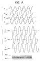
- FIG. 9 shows an example of wavelengths of output signals of the I-V conversion circuits 41 to 44 in the case where a light contrast pattern moves on the photodiode array and there occurs fluctuations in light intensity. From the I-V conversion circuits 41, 42, 43, and 44, there are obtained similar signal waveforms although their phases differ from each other.
- Reference numerals 2a and 2c denote signals whose phases are shifted from each other by 180°. With these signals, it is possible to obtain, from a result of addition of the signals 2a to 2c, a reference signal for performing feedback of the intensity of light emitted from the light source.
- the MRA reflection scale 3 possesses a function of converting a divergent light beam into a convergent light beam that has been unattainable by the conventional reflection-type scale.
- a light transmission portion (corresponding to 3c) and light reflecting portions (corresponding to 3a n , 3b n ) are provided at constant periods, so that there is realized the same optical action as a diffraction grating of an amplitude type, as is the case of the conventional reflection-type optical scale.
- a diffraction interference phenomenon in compliance with the three-grating-type optical principle that is known in the prior art.
- a light beam emitted from the light source means and reflected, diffracted, and interfered by the MRA reflection scale 3 forms a grating image (diffracted and interfered image) on the photodiode portions S1 to S3 of the semiconductor base 2, with the grating image being determined by the grating pitch P 1 of the MRA scale, the arrangement intervals P 2 between the plurality of light-emitting regions, and the luminescence center wavelength ⁇ of the light source.
- the pitch of the grating image is P 2 (approximately equal to 168 ⁇ m) and exhibits a value that is twice as great as P 1 , and the segment pitch of the light-receiving means is set at P 2 and overlaps the pitch P 2 of the grating image.
- FIG. 10B shows a relation between the received light intensity and the gaps.
- the peak of the received light intensity is exhibited at a position of around 2 mm and it is scarcely possible to secure a practical light intensity with a distance of 5 mm or longer.
- the gap is set at a position in proximity to "0" in the graph shown in FIG. 10A.
- FIG. 10C is a characteristic drawing showing the changing of an output signal amplitude obtained from results of actual experiments.
- the output signal amplitude becomes the maximum, thereby obtaining a favorable characteristic.
- a second embodiment differs from the first embodiment described above only in a size relation in a manner described below.
- P 1 that is the pitch of the MRA scale is approximately equal to 42 ⁇ m
- P 2 that is the arrangement pitch of the array-shaped light source/the pitch between the segments (S1, S2, and S3) of the photodiode array is approximately equal to 84 ⁇ m.
- a preferable gap setting position will be calculated by concretely assuming important numerical values in the second embodiment, as is the case of the first embodiment described above.
- FIG. 10D shows results of experiments conducted in the second embodiment.
- the received light intensity becomes very low.
- the peak of the output signal is obtained in a range of n ⁇ 1, and the maximum amplitude exists at around 1.0 mm in this case.
- the maximum amplitude exists in proximity to the received light intensity peak position that is around 2 mm.
- a valley of the contrast value exists in proximity to the peak position of the received light intensity, so that the maximum amplitude position deviates from the peak of the received light intensity, and the signal amplitude peak exists in proximity to 1 mm.
- a third embodiment differs from the first embodiment only in a size relation in a manner described below, as is the case of the second embodiment.
- P 1 that is the pitch of the MRA scale is approximately equal to 21 ⁇ m
- P 2 that is the arrangement pitch of the array-shaped light source/the pitch between segments (S1 S2,and S3) of the photodiode array is approximately equal to 42 ⁇ m.
- a preferable gap setting position will be calculated by concretely assuming important numerical values in the third embodiment, as is the case of the first embodiment described above.
- FIG. 10E shows results of experiments conducted in the third embodiment.
- the peak of an output signal is obtained at a position of 1.357 mm.
- an effective gap position is given within a range of 0.5 ⁇ n ⁇ 1.5.
- Conditional Expression (6) has been hitherto regarded as preferable in the case of the three-grating-type and reflection-type construction. When a substantial signal amplitude is considered, however, it is impossible to say that the arrangement derived from this Conditional Expression (6) is necessarily optimum.
- the peak position of the received light intensity is critical, and the optimum arrangement is determined in a relation between the contrast peak position obtained from Conditional Expression (6) and this received light intensity peak position.
- the received light intensity peak position is controlled by changing the arrangement relation between the light source means and the light-receiving means so that the peak position of the received light intensity coincides with the contrast peak position, thereby making an attempt to obtain an output signal having the maximum amplitude with which these peak positions coincide with each other. Therefore, it is possible to realize this embodiment with the means described above.
- n in Conditional Expression (6) has been hitherto considered within a range of natural numbers. If the possible reflection scale pitch is set at around 84 ⁇ m or 42 ⁇ m as is the case of the first or second embodiment, the best position exists within a range of n ⁇ 1 or n ⁇ 0.5, with the peak position of the received light intensity being more dominance than the contrast peak position. Also, when the pitch is set at around 21 ⁇ m as described in the third embodiment, it is preferable that a relation is realized with which the contrast peak position coincides with the received light intensity peak position.
- FIG. 10F collectively shows the results obtained in the first to third embodiments. Fourth Embodiment
- FIG. 11 When Ra is set at 90° and the pitch Pm is set at a size with which no problem occurs, a construction shown in FIG. 11 is applicable as an example of a realizable arrangement construction of the light-emitting means 1 and the light-receiving means 2.
- the reflection scale 3 is produced using a translucent member and the angle Ra is set at 90°.
- a chip of the LED 1 is mounted and implemented on the silicon photodiode chip of the light-receiving element 2, which makes it possible to avoid the problems described above. It is possible to say that this construction is preferable when its high mounting density is considered, although it is required to give consideration to heat generation of the LED 1.
- an angle offset is given (set at an angle larger than 90°), and the silicon photodiode 2 and the LED chip 1 are mounted on the same mounting surface in parallel, as shown in FIG. 14.
- FIGS. 12A to 14B are each an explanatory drawing related to another embodiment of the MRA reflection scale functioning as the reflecting means.
- FIG. 12A shows a basic construction (Ra is set at 95°) for comparison.
- FIG. 12B relates to this fifth embodiment and shows a state where V-letter shaped grooves are arranged along a cylindrical surface CL (partial surface of a cylinder.) .
- This arrangement is effective when a translucent member is used and, in comparison with the construction in FIG. 12A with which limitations tend to be imposed on the condition of total reflection, it is possible to widen an allowable range of an incident angle of a light beam onto the surfaces of the V-letter shaped grooves.
- FIG. 12C relates to a sixth embodiment and shows an example in which the V-letter shaped grooves are arranged in a straight line manner while maintaining the directions of respective V-letter shaped grooves in FIG. 12B (angle directions indicated by the alternate long and short dash lines).
- the reflecting body is bent and therefore increases in thickness. In this example, however, this problem is solved.
- the concept of the present invention is applicable not only to the V-letter shaped grooves but also to an example of FIG. 13A (seventh embodiment), or a modification thereof, which is shown in FIG. 13B (eighth embodiment).
- FIG. 13A relates to a seventh embodiment and shows an example of a one-dimensional convergent reflecting element obtained by forming a reflecting film on a cylindrical surface CL through evaporation of aluminum or the like.
- a one-dimensional convergent reflecting element obtained by forming a reflecting film on a cylindrical surface CL through evaporation of aluminum or the like.
- FIG. 13B relates to an eighth embodiment and shows a construction where the cylindrical surface CL is divided into curved surfaces having different curvatures, and the curved surfaces are combined with each other, thereby avoiding the problem that the thickness is increased.
- a reflecting film is applied to each surface obtained by dividing the cylindrical surface CL.
- FIGS. 13A and 13B As can be seen by comparing FIGS. 13A and 13B with each other under a condition where the one-dimensional convergent reflecting element is confined within a certain thickness, if the thickness is the same, a range, in which it is possible to guide a light beam from the light source to a light-receiving portion, is widened by around 10° in the case of FIG. 13B in which the cylindrical curved surface is divided. As a result of this modification, the usage efficiency of light intensity is further enhanced.
- FIG. 14A shows a case where a reflection-type Fresnel zone plate is used as the reflecting body.
- a reflecting surface is formed in a reflecting portion 105(A) by utilizing an internal total reflection action of the V-letter shaped grooves.
- FIG. 14B shows a case where the aforementioned construction in FIG. 13B is further improved.
- no aluminum reflecting film is applied to the divided cylindrical surface CL, and reflecting surfaces are substantially formed by utilizing the internal total reflection action of the V-letter shaped grooves.
- FIG. 15 shows a construction where the aforementioned reflecting body 3 having the one-dimensional convergent reflecting element in FIG. 12C is applied as a reflection scale for a linear encoder.
- reference numeral 1 denotes a light source of a photosensor PS
- reference numeral 2 indicates a light-receiving portion of the photosensor PS.
- FIGS. 16, 17A, and 17B according to the construction of the first embodiment where the reflection scale 3 of the reflection-type linear encoder is produced by periodically providing the V-letter shaped groove group OE for a translucent member TT1, the cylindrical surface CL is integrally or independently provided on the underside of the transparent substrate, thereby enhancing the light usage efficiency.
- Its 17A-17A cross-sectional view and 17B-17B cross-sectional view are respectively shown in FIGS. 17A and 17B.
- a divergent light beam from a light source is converted on the cylindrical surface CL into an almost parallel light beam, repeats internal total reflection twice on the V-letter shaped groove surface, is converted into a convergent light beam while passing through the cylindrical surface CL again, and is guided to a light-receiving portion (not shown).
- FIG. 18 is an explanatory drawing of a comparison result on a relation between (a) a distance between a photosensor in the case where the reflecting body having the one-dimensional convergence reflecting element of the present invention that has been hitherto explained is applied to, for instance, an encoder and the reflecting body and (b) the value of a photo current generated when the light-receiving portion of the photosensor detects light, a relation in the case of using a conventional reflecting plate (reflecting body produced by evaporating aluminum to a flat plate).
- a conventional reflecting plate reflecting body produced by evaporating aluminum to a flat plate
- FIG. 35 shows an example in which a video lens system is formed using a voice coil actuator.
- a lens group 801b of variator lenses for magnification and a lens group 801d of focus lenses are driven using the voice coil actuator, and encoders for zooming 816a and 820 and encoders for auto-focusing 816b and 821 are attached to detect the absolute positions of the lens groups 801b and 801d.
- the construction elements 816a and 816b are each a linear encoder scale of an embodiment of the present invention, while the construction elements 820 and 821 are each the detecting head of an embodiment of the present invention.
- Outputs from the detecting heads 820 and 821 are respectively read by reading circuits 822 and 823 and are sent to a CPU 824. Also, information concerning a focus state is sent to the CPU 824 through a reading circuit 826 by means of a video signal from a CCD 825.
- the CPU 824 determines the value or waveform of a current that should be allowed to pass through each voice coil based on the received information as well as information prestored in a ROM 827 and energizes the coils 816a and 816b through their corresponding drivers 828 and 829. With this system, the lens group 801b and the lens group 801d are positioned so that an in-focus state is always maintained.
- the construction elements 820 and 821 are equipped with the detecting head of the present invention.
- the sensitivity of the optical system to positioning tends to be increased in accordance with a reduction in size, so that a high-resolution and high-accuracy encoder becomes necessary.
- the low-power consumption encoder embodying the present invention has an important effect in view of application as well as the aforementioned features.
- the encoders 820 and 821 there has been used a type, in which a brush traces an electrode for which a linear-type volume or a gray code pattern has been formed, or a type in which position detection is performed using a photoelectric conversion element, such as a PSD, and an optical element that moves along with a lens holding frame.
- a photoelectric conversion element such as a PSD
- an optical encoder embodying the present invention By applying an optical encoder embodying the present invention, it becomes possible to perform position detection in a non-contact manner and also to realize a significant reduction in mounting space. As a result, there is enhanced flexibility in designing a lens-barrel.
- FIG. 36 shows an example in which the optical reflection encoder scale and head embodying the present invention are used in order to control driving of a print head of an ink jet printer.
- reference numeral 701 denotes a case, numeral 505 a carriage unit containing a print head, an ink tank, and the like, numeral 705 a guiding rod, numeral 703 a drive motor for transporting paper, numeral 703 a gear on a drive axis, numeral 704 an idler gear, numeral 603 a gear placed on the main axis of a transport roller.
- an encoder for detecting a rotation angle is also placed on this axis.
- a linear encoder scale 502 of an embodiment of the present invention extends parallel to the guiding rod 705, with one end thereof being fixed to the case 701 and the other end being fixed to the case 701 through a not-shown plate spring.
- the scale 502 in this embodiment is produced by providing a transparent film made of transparent polycarbonate with the minute groove shape at predetermined intervals.
- FIG. 37 is an explanatory drawing of the encoder portion of the present embodiment placed on the carriage.
- reference numeral 502 denotes the linear encoder scale of the present embodiment that is placed in the case 701 shown in FIG. 36
- numeral 503 a detecting head of the present embodiment that is mounted on a substrate 506 attached to the carriage 504 along with a drive circuit for driving an ink jet head and the like.
- the detecting head embodying the present invention has a ultra-small size, and therefore it is easy to mount this detecting head. That is, it is easy to embed the present detecting head into a printer, in comparison with a conventional transmission-type encoder. From the viewpoint of low power consumption, the application to a mobile printer or the like becomes a further effective means.
- FIG. 38 shows a state where the printer is viewed from a side thereof.
- a rotary encoder scale 602 that is mounted and hidden behind a main paper transport roller drive gear, a detecting head 601, and a base 603 on which the detecting head 601 is mounted.
- embodiments of the present invention it becomes possible to realize high-resolution and high-precision electrical division, which in turn makes it possible to reduce the diameter of a rotary encoder scale for performing angle detection.
- a large-diameter encoder scale has been hitherto used in order to detect paper sending position with high resolution, it becomes possible to reduce the size of the rotary encoder scale so as to become smaller than the diameter of a gear for driving, as shown in this drawing.
- an apparatus or the like such as a mobile printer, for which it is required to perform designing for ultra-miniaturization
- embodiments of the present invention achieve a particularly enormous effect.
- the application of embodiments of the present invention to a mobile printer or the like becomes a further effective means even from the viewpoint of low power consumption.
- a reflecting element provided for a reflecting body that is the target of measurement and observation
- an optical apparatus such as an encoder
- the reflecting body When the reflecting body is used as a marker member for an optical sensor/optical scale, there is obtained a high light transmission efficiency between light emission and light reception.
- a sensor embodying the present invention to various kinds of information devices, video devices, and the like, it becomes possible to detect displacement information containing the moving direction of a moving body with high precision while realizing overall simplification, miniaturization, and reduction in power consumption of an apparatus.
Applications Claiming Priority (2)
| Application Number | Priority Date | Filing Date | Title |
|---|---|---|---|
| JP2002145920 | 2002-05-21 | ||
| JP2002145920A JP4208483B2 (ja) | 2002-05-21 | 2002-05-21 | 光学式エンコーダ |
Publications (1)
| Publication Number | Publication Date |
|---|---|
| EP1365214A1 true EP1365214A1 (de) | 2003-11-26 |
Family
ID=29397787
Family Applications (1)
| Application Number | Title | Priority Date | Filing Date |
|---|---|---|---|
| EP03253116A Withdrawn EP1365214A1 (de) | 2002-05-21 | 2003-05-19 | Sensor mit einem, aus einem Array von Dachkantenspiegel und -prismen, bestehenden Massstab, und Apparatus mit einem derartigen Sensor |
Country Status (3)
| Country | Link |
|---|---|
| US (2) | US7022974B2 (de) |
| EP (1) | EP1365214A1 (de) |
| JP (1) | JP4208483B2 (de) |
Cited By (8)
| Publication number | Priority date | Publication date | Assignee | Title |
|---|---|---|---|---|
| DE102005004419A1 (de) * | 2005-01-31 | 2006-08-03 | Sick Ag | Optoelektronischer Sensor |
| EP1688711A2 (de) * | 2005-02-04 | 2006-08-09 | Canon Kabushiki Kaisha | Optischer Kodierer |
| EP2169357A1 (de) * | 2008-09-24 | 2010-03-31 | CSEM Centre Suisse d'Electronique et de Microtechnique SA Recherche et Développement | Zweidimensionaler Positionsanzeiger |
| CN102155915A (zh) * | 2010-12-31 | 2011-08-17 | 东莞康视达自动化科技有限公司 | 多波段光学在线尺寸检测方法及系统 |
| KR101289805B1 (ko) * | 2012-03-19 | 2013-08-14 | 주식회사 져스텍 | 랜덤 코드 및 프레넬 존 플레이트를 이용한 광학 인코더의 영점 검출 장치 |
| CN103376123A (zh) * | 2012-04-27 | 2013-10-30 | 佳能株式会社 | 编码器、透镜装置和照相机 |
| JP2013239578A (ja) * | 2012-05-15 | 2013-11-28 | Omron Corp | 光電センサ |
| CN103512597A (zh) * | 2012-06-29 | 2014-01-15 | 佳能株式会社 | 编码器、镜头装置和照相机 |
Families Citing this family (36)
| Publication number | Priority date | Publication date | Assignee | Title |
|---|---|---|---|---|
| EP1235054B1 (de) * | 2001-02-20 | 2011-09-21 | Canon Kabushiki Kaisha | Optisches Wegmessungsvorrichtung |
| JP4343556B2 (ja) * | 2003-03-05 | 2009-10-14 | キヤノン株式会社 | 光学式エンコーダ |
| JP2005064625A (ja) * | 2003-08-19 | 2005-03-10 | Pioneer Electronic Corp | 信号調整装置 |
| JP4209279B2 (ja) * | 2003-08-19 | 2009-01-14 | パイオニア株式会社 | 信号調整装置 |
| JP4418278B2 (ja) * | 2004-03-30 | 2010-02-17 | オリンパス株式会社 | 光学式エンコーダ及びその製造方法 |
| US7667186B2 (en) * | 2004-05-28 | 2010-02-23 | Nokia Corporation | Optoelectronic position determination system |
| JP4498024B2 (ja) * | 2004-06-15 | 2010-07-07 | キヤノン株式会社 | 光学式エンコーダ |
| US7332709B2 (en) * | 2004-12-13 | 2008-02-19 | Nikon Corporation | Photoelectric encoder |
| JP4847031B2 (ja) * | 2005-03-14 | 2011-12-28 | キヤノン株式会社 | 光学式エンコーダ |
| US7253384B2 (en) * | 2005-03-23 | 2007-08-07 | Microscan Systems Incorporated | Focusing system using light source and image sensor |
| US7193697B2 (en) * | 2005-07-25 | 2007-03-20 | Chroma Ate Inc. | Apparatus for feature detection |
| JP2008028025A (ja) | 2006-07-19 | 2008-02-07 | Canon Inc | 反射型センサ |
| DE102006049178A1 (de) * | 2006-10-18 | 2008-04-30 | Sensopart Industriesensorik Gmbh | Optoelektronische Sensorvorrichtung |
| BRPI0720784A2 (pt) * | 2007-01-11 | 2014-01-28 | 3M Innovative Properties Co | Sensor de manta em posição longitudinal |
| EP2165162A2 (de) * | 2007-06-19 | 2010-03-24 | 3M Innovative Properties Company | Totalreflektions-verschiebungsskala |
| KR101493115B1 (ko) * | 2007-06-19 | 2015-02-12 | 쓰리엠 이노베이티브 프로퍼티즈 컴파니 | 웨브의 위치를 나타내는 시스템 및 방법 |
| CN101688794B (zh) * | 2007-06-19 | 2012-12-12 | 3M创新有限公司 | 用于制造位移刻度尺的系统和方法 |
| NL1036323A1 (nl) * | 2007-12-27 | 2009-06-30 | Asml Holding Nv | Folded optical encoder and applications for same. |
| JP5058845B2 (ja) * | 2008-02-25 | 2012-10-24 | キヤノン株式会社 | 変位検出装置及びそれを有する光学機器 |
| WO2010077592A2 (en) | 2008-12-29 | 2010-07-08 | 3M Innovative Properties Company | Phase-locked web position signal using web fiducials |
| SG172781A1 (en) | 2008-12-30 | 2011-08-29 | 3M Innovative Properties Co | Apparatus and method for making fiducials on a substrate |
| JP5460352B2 (ja) * | 2010-01-22 | 2014-04-02 | キヤノン株式会社 | 変位測定装置および速度測定装置 |
| JP5479435B2 (ja) * | 2011-01-31 | 2014-04-23 | 日本電産コパル株式会社 | レンズ駆動装置及び撮像装置 |
| JP5868058B2 (ja) * | 2011-07-28 | 2016-02-24 | キヤノン株式会社 | 位置計測装置、光学部品の製造方法、および型の製造方法 |
| JP5941268B2 (ja) * | 2011-11-10 | 2016-06-29 | キヤノン株式会社 | 発光素子駆動回路、光学式エンコーダ、カメラ及び発光素子駆動回路の制御方法 |
| EP2639615A1 (de) * | 2012-03-13 | 2013-09-18 | Leica Geosystems AG | Kamerasystem mit einem Zoomobjektiv und einem Linearencoder |
| JP2013222032A (ja) * | 2012-04-16 | 2013-10-28 | Olympus Imaging Corp | 光検出装置 |
| JP6020583B2 (ja) * | 2012-10-11 | 2016-11-02 | ソニー株式会社 | 位置検出装置、レンズ鏡筒、撮像装置 |
| CN104180827A (zh) * | 2013-05-23 | 2014-12-03 | 株式会社精工技研 | 光学式编码器的代码板 |
| JP5832562B2 (ja) * | 2014-01-24 | 2015-12-16 | ファナック株式会社 | 樹脂製コード板を有する反射型光学式エンコーダ |
| JP2016057346A (ja) * | 2014-09-05 | 2016-04-21 | 株式会社アスカネット | 再帰性反射体及びその製造方法 |
| FR3031588B1 (fr) * | 2015-01-13 | 2018-11-16 | Hutchinson | Capteurs inductifs de deplacement |
| US11499848B2 (en) * | 2016-03-31 | 2022-11-15 | Pixart Imaging Inc. | Marker product and related optical detection system |
| JP6932983B2 (ja) * | 2017-05-01 | 2021-09-08 | セイコーエプソン株式会社 | エンコーダースケール、エンコーダースケールの製造方法、エンコーダー、ロボットおよびプリンター |
| CN108444396B (zh) * | 2018-05-18 | 2024-02-06 | 北方民族大学 | 光路一致式位移传感器及其测量方法 |
| TWI692336B (zh) * | 2019-04-24 | 2020-05-01 | 萬物智得股份有限公司 | 手沖咖啡動作記錄裝置 |
Citations (5)
| Publication number | Priority date | Publication date | Assignee | Title |
|---|---|---|---|---|
| WO2001063215A1 (en) * | 2000-02-23 | 2001-08-30 | Renishaw Plc | Opto-electronic scale reading apparatus |
| JP2001284639A (ja) * | 2000-03-31 | 2001-10-12 | Hitachi Cable Ltd | プリンター用発光ダイオードアレイ |
| US20020000515A1 (en) | 2000-04-17 | 2002-01-03 | Manabu Takayama | Optical scale, mold therefor, and optical encoder |
| EP1184645A1 (de) * | 2000-08-29 | 2002-03-06 | Abb Research Ltd. | Optischer Winkel- oder Wegmessgeber |
| EP1235054A2 (de) | 2001-02-20 | 2002-08-28 | Canon Kabushiki Kaisha | Reflexionsskala und Wegmessungsvorrichtung |
Family Cites Families (2)
| Publication number | Priority date | Publication date | Assignee | Title |
|---|---|---|---|---|
| JPS5830725A (ja) * | 1981-08-17 | 1983-02-23 | Ricoh Co Ltd | ダハミラ−アレイ |
| US4736225A (en) * | 1985-07-17 | 1988-04-05 | Minolta Camera Kabushiki Kaisha | Slit exposure projection device |
-
2002
- 2002-05-21 JP JP2002145920A patent/JP4208483B2/ja not_active Expired - Fee Related
-
2003
- 2003-05-19 US US10/441,862 patent/US7022974B2/en not_active Expired - Fee Related
- 2003-05-19 EP EP03253116A patent/EP1365214A1/de not_active Withdrawn
-
2005
- 2005-08-30 US US11/216,900 patent/US7045770B2/en not_active Expired - Lifetime
Patent Citations (5)
| Publication number | Priority date | Publication date | Assignee | Title |
|---|---|---|---|---|
| WO2001063215A1 (en) * | 2000-02-23 | 2001-08-30 | Renishaw Plc | Opto-electronic scale reading apparatus |
| JP2001284639A (ja) * | 2000-03-31 | 2001-10-12 | Hitachi Cable Ltd | プリンター用発光ダイオードアレイ |
| US20020000515A1 (en) | 2000-04-17 | 2002-01-03 | Manabu Takayama | Optical scale, mold therefor, and optical encoder |
| EP1184645A1 (de) * | 2000-08-29 | 2002-03-06 | Abb Research Ltd. | Optischer Winkel- oder Wegmessgeber |
| EP1235054A2 (de) | 2001-02-20 | 2002-08-28 | Canon Kabushiki Kaisha | Reflexionsskala und Wegmessungsvorrichtung |
Non-Patent Citations (1)
| Title |
|---|
| SAWADA R ET AL: "MONOLITHIC-INTEGRATED MICROLASER ENCODER", APPLIED OPTICS, OPTICAL SOCIETY OF AMERICA,WASHINGTON, US, vol. 38, no. 33, 20 November 1999 (1999-11-20), pages 6866 - 6873, XP000903742, ISSN: 0003-6935 * |
Cited By (16)
| Publication number | Priority date | Publication date | Assignee | Title |
|---|---|---|---|---|
| DE102005004419A1 (de) * | 2005-01-31 | 2006-08-03 | Sick Ag | Optoelektronischer Sensor |
| US7463419B2 (en) | 2005-01-31 | 2008-12-09 | Sick Ag | Optoelectronic sensor |
| EP1688711A2 (de) * | 2005-02-04 | 2006-08-09 | Canon Kabushiki Kaisha | Optischer Kodierer |
| EP1688711A3 (de) * | 2005-02-04 | 2012-05-02 | Canon Kabushiki Kaisha | Optischer Kodierer |
| EP2169357A1 (de) * | 2008-09-24 | 2010-03-31 | CSEM Centre Suisse d'Electronique et de Microtechnique SA Recherche et Développement | Zweidimensionaler Positionsanzeiger |
| CN102155915A (zh) * | 2010-12-31 | 2011-08-17 | 东莞康视达自动化科技有限公司 | 多波段光学在线尺寸检测方法及系统 |
| CN102155915B (zh) * | 2010-12-31 | 2013-01-23 | 东莞科视自动化科技有限公司 | 多波段光学在线尺寸检测方法及系统 |
| KR101289805B1 (ko) * | 2012-03-19 | 2013-08-14 | 주식회사 져스텍 | 랜덤 코드 및 프레넬 존 플레이트를 이용한 광학 인코더의 영점 검출 장치 |
| CN103376123A (zh) * | 2012-04-27 | 2013-10-30 | 佳能株式会社 | 编码器、透镜装置和照相机 |
| EP2657655A3 (de) * | 2012-04-27 | 2014-06-11 | Canon Kabushiki Kaisha | Kodierer, Linsenvorrichtung und Kamera |
| CN103376123B (zh) * | 2012-04-27 | 2016-01-20 | 佳能株式会社 | 编码器、透镜装置和照相机 |
| US9329058B2 (en) | 2012-04-27 | 2016-05-03 | Canon Kabushiki Kaisha | Encoder that detects displacement of an object, and lens apparatus and camera having the same |
| JP2013239578A (ja) * | 2012-05-15 | 2013-11-28 | Omron Corp | 光電センサ |
| CN103512597A (zh) * | 2012-06-29 | 2014-01-15 | 佳能株式会社 | 编码器、镜头装置和照相机 |
| US9116020B2 (en) | 2012-06-29 | 2015-08-25 | Canon Kabushiki Kaisha | Encoder, lens apparatus, and camera capable of detecting position of object |
| CN103512597B (zh) * | 2012-06-29 | 2016-05-11 | 佳能株式会社 | 编码器、镜头装置和照相机 |
Also Published As
| Publication number | Publication date |
|---|---|
| JP2003337052A (ja) | 2003-11-28 |
| US20030218125A1 (en) | 2003-11-27 |
| JP4208483B2 (ja) | 2009-01-14 |
| US20060028653A1 (en) | 2006-02-09 |
| US7022974B2 (en) | 2006-04-04 |
| US7045770B2 (en) | 2006-05-16 |
Similar Documents
| Publication | Publication Date | Title |
|---|---|---|
| EP1365214A1 (de) | Sensor mit einem, aus einem Array von Dachkantenspiegel und -prismen, bestehenden Massstab, und Apparatus mit einem derartigen Sensor | |
| EP1382941B1 (de) | Gitterkodierer mit faseroptischen Empfängerkanälen und Vorrichtung zur Messung einer Verlagerung | |
| US9618370B2 (en) | Optical encoder and apparatus provided therewith | |
| JP4724496B2 (ja) | 光学式エンコーダ | |
| US7622698B2 (en) | Detection head | |
| US20080173800A1 (en) | Optical encoder and optical lens module | |
| US8710425B2 (en) | Encoder that optically detects positional information of a moving body from different optical paths lengths | |
| EP1475613B1 (de) | Kodierer mit faseroptischen Empfängerkanälen | |
| US9347802B2 (en) | Scale, vernier encoder and apparatus using the same | |
| JP2013003146A (ja) | 変位センサ | |
| US7995212B2 (en) | Optical displacement measuring device | |
| JP2006292728A (ja) | 光電式エンコーダ | |
| US7230726B2 (en) | Scanning unit for a position measuring instrument for optical scanning of a object measuring graduation | |
| EP2023095B1 (de) | Fixpunktdetektor und Verschiebungsmesser | |
| JP2007315919A (ja) | エンコーダ | |
| JP2002243503A (ja) | 光学式エンコーダ | |
| US9366550B2 (en) | Optical encoder having a scale comprising a light guiding portion with reflection surfaces and a light guiding function | |
| JP4416560B2 (ja) | 光学式変位測定装置 | |
| JPH10213455A (ja) | 光学式リニアエンコーダ | |
| JPH11154019A (ja) | リニア駆動装置 | |
| JP2005090997A (ja) | 光学式エンコーダとその信号安定化方法 |
Legal Events
| Date | Code | Title | Description |
|---|---|---|---|
| PUAI | Public reference made under article 153(3) epc to a published international application that has entered the european phase |
Free format text: ORIGINAL CODE: 0009012 |
|
| AK | Designated contracting states |
Kind code of ref document: A1 Designated state(s): AT BE BG CH CY CZ DE DK EE ES FI FR GB GR HU IE IT LI LU MC NL PT RO SE SI SK TR |
|
| AX | Request for extension of the european patent |
Extension state: AL LT LV MK |
|
| 17P | Request for examination filed |
Effective date: 20040426 |
|
| AKX | Designation fees paid |
Designated state(s): DE FR GB |
|
| 17Q | First examination report despatched |
Effective date: 20110120 |
|
| GRAP | Despatch of communication of intention to grant a patent |
Free format text: ORIGINAL CODE: EPIDOSNIGR1 |
|
| INTG | Intention to grant announced |
Effective date: 20160811 |
|
| STAA | Information on the status of an ep patent application or granted ep patent |
Free format text: STATUS: THE APPLICATION HAS BEEN WITHDRAWN |
|
| 18W | Application withdrawn |
Effective date: 20161215 |