EP1251607B1 - Semiconductor laser module, spatial optical transmission system and electronic appliance - Google Patents
Semiconductor laser module, spatial optical transmission system and electronic appliance Download PDFInfo
- Publication number
- EP1251607B1 EP1251607B1 EP02252736A EP02252736A EP1251607B1 EP 1251607 B1 EP1251607 B1 EP 1251607B1 EP 02252736 A EP02252736 A EP 02252736A EP 02252736 A EP02252736 A EP 02252736A EP 1251607 B1 EP1251607 B1 EP 1251607B1
- Authority
- EP
- European Patent Office
- Prior art keywords
- receiving element
- light receiving
- wavelength
- light
- semiconductor laser
- Prior art date
- Legal status (The legal status is an assumption and is not a legal conclusion. Google has not performed a legal analysis and makes no representation as to the accuracy of the status listed.)
- Expired - Lifetime
Links
Images


Classifications
-
- H—ELECTRICITY
- H04—ELECTRIC COMMUNICATION TECHNIQUE
- H04B—TRANSMISSION
- H04B10/00—Transmission systems employing electromagnetic waves other than radio-waves, e.g. infrared, visible or ultraviolet light, or employing corpuscular radiation, e.g. quantum communication
- H04B10/11—Arrangements specific to free-space transmission, i.e. transmission through air or vacuum
-
- B—PERFORMING OPERATIONS; TRANSPORTING
- B82—NANOTECHNOLOGY
- B82Y—SPECIFIC USES OR APPLICATIONS OF NANOSTRUCTURES; MEASUREMENT OR ANALYSIS OF NANOSTRUCTURES; MANUFACTURE OR TREATMENT OF NANOSTRUCTURES
- B82Y20/00—Nanooptics, e.g. quantum optics or photonic crystals
-
- H—ELECTRICITY
- H01—ELECTRIC ELEMENTS
- H01S—DEVICES USING THE PROCESS OF LIGHT AMPLIFICATION BY STIMULATED EMISSION OF RADIATION [LASER] TO AMPLIFY OR GENERATE LIGHT; DEVICES USING STIMULATED EMISSION OF ELECTROMAGNETIC RADIATION IN WAVE RANGES OTHER THAN OPTICAL
- H01S5/00—Semiconductor lasers
- H01S5/02—Structural details or components not essential to laser action
- H01S5/022—Mountings; Housings
- H01S5/0225—Out-coupling of light
- H01S5/02253—Out-coupling of light using lenses
-
- H—ELECTRICITY
- H10—SEMICONDUCTOR DEVICES; ELECTRIC SOLID-STATE DEVICES NOT OTHERWISE PROVIDED FOR
- H10F—INORGANIC SEMICONDUCTOR DEVICES SENSITIVE TO INFRARED RADIATION, LIGHT, ELECTROMAGNETIC RADIATION OF SHORTER WAVELENGTH OR CORPUSCULAR RADIATION
- H10F30/00—Individual radiation-sensitive semiconductor devices in which radiation controls the flow of current through the devices, e.g. photodetectors
- H10F30/20—Individual radiation-sensitive semiconductor devices in which radiation controls the flow of current through the devices, e.g. photodetectors the devices having potential barriers, e.g. phototransistors
- H10F30/21—Individual radiation-sensitive semiconductor devices in which radiation controls the flow of current through the devices, e.g. photodetectors the devices having potential barriers, e.g. phototransistors the devices being sensitive to infrared, visible or ultraviolet radiation
- H10F30/22—Individual radiation-sensitive semiconductor devices in which radiation controls the flow of current through the devices, e.g. photodetectors the devices having potential barriers, e.g. phototransistors the devices being sensitive to infrared, visible or ultraviolet radiation the devices having only one potential barrier, e.g. photodiodes
- H10F30/223—Individual radiation-sensitive semiconductor devices in which radiation controls the flow of current through the devices, e.g. photodetectors the devices having potential barriers, e.g. phototransistors the devices being sensitive to infrared, visible or ultraviolet radiation the devices having only one potential barrier, e.g. photodiodes the potential barrier being a PIN barrier
-
- H—ELECTRICITY
- H10—SEMICONDUCTOR DEVICES; ELECTRIC SOLID-STATE DEVICES NOT OTHERWISE PROVIDED FOR
- H10F—INORGANIC SEMICONDUCTOR DEVICES SENSITIVE TO INFRARED RADIATION, LIGHT, ELECTROMAGNETIC RADIATION OF SHORTER WAVELENGTH OR CORPUSCULAR RADIATION
- H10F55/00—Radiation-sensitive semiconductor devices covered by groups H10F10/00, H10F19/00 or H10F30/00 being structurally associated with electric light sources and electrically or optically coupled thereto
- H10F55/20—Radiation-sensitive semiconductor devices covered by groups H10F10/00, H10F19/00 or H10F30/00 being structurally associated with electric light sources and electrically or optically coupled thereto wherein the electric light source controls the radiation-sensitive semiconductor devices, e.g. optocouplers
- H10F55/25—Radiation-sensitive semiconductor devices covered by groups H10F10/00, H10F19/00 or H10F30/00 being structurally associated with electric light sources and electrically or optically coupled thereto wherein the electric light source controls the radiation-sensitive semiconductor devices, e.g. optocouplers wherein the radiation-sensitive devices and the electric light source are all semiconductor devices
-
- H—ELECTRICITY
- H10—SEMICONDUCTOR DEVICES; ELECTRIC SOLID-STATE DEVICES NOT OTHERWISE PROVIDED FOR
- H10F—INORGANIC SEMICONDUCTOR DEVICES SENSITIVE TO INFRARED RADIATION, LIGHT, ELECTROMAGNETIC RADIATION OF SHORTER WAVELENGTH OR CORPUSCULAR RADIATION
- H10F77/00—Constructional details of devices covered by this subclass
- H10F77/10—Semiconductor bodies
- H10F77/12—Active materials
-
- H—ELECTRICITY
- H01—ELECTRIC ELEMENTS
- H01S—DEVICES USING THE PROCESS OF LIGHT AMPLIFICATION BY STIMULATED EMISSION OF RADIATION [LASER] TO AMPLIFY OR GENERATE LIGHT; DEVICES USING STIMULATED EMISSION OF ELECTROMAGNETIC RADIATION IN WAVE RANGES OTHER THAN OPTICAL
- H01S5/00—Semiconductor lasers
- H01S5/02—Structural details or components not essential to laser action
- H01S5/022—Mountings; Housings
- H01S5/02218—Material of the housings; Filling of the housings
- H01S5/02234—Resin-filled housings; the housings being made of resin
-
- H—ELECTRICITY
- H01—ELECTRIC ELEMENTS
- H01S—DEVICES USING THE PROCESS OF LIGHT AMPLIFICATION BY STIMULATED EMISSION OF RADIATION [LASER] TO AMPLIFY OR GENERATE LIGHT; DEVICES USING STIMULATED EMISSION OF ELECTROMAGNETIC RADIATION IN WAVE RANGES OTHER THAN OPTICAL
- H01S5/00—Semiconductor lasers
- H01S5/10—Construction or shape of the optical resonator, e.g. extended or external cavity, coupled cavities, bent-guide, varying width, thickness or composition of the active region
- H01S5/1082—Construction or shape of the optical resonator, e.g. extended or external cavity, coupled cavities, bent-guide, varying width, thickness or composition of the active region with a special facet structure, e.g. structured, non planar, oblique
- H01S5/1085—Oblique facets
-
- H—ELECTRICITY
- H01—ELECTRIC ELEMENTS
- H01S—DEVICES USING THE PROCESS OF LIGHT AMPLIFICATION BY STIMULATED EMISSION OF RADIATION [LASER] TO AMPLIFY OR GENERATE LIGHT; DEVICES USING STIMULATED EMISSION OF ELECTROMAGNETIC RADIATION IN WAVE RANGES OTHER THAN OPTICAL
- H01S5/00—Semiconductor lasers
- H01S5/20—Structure or shape of the semiconductor body to guide the optical wave ; Confining structures perpendicular to the optical axis, e.g. index or gain guiding, stripe geometry, broad area lasers, gain tailoring, transverse or lateral reflectors, special cladding structures, MQW barrier reflection layers
- H01S5/22—Structure or shape of the semiconductor body to guide the optical wave ; Confining structures perpendicular to the optical axis, e.g. index or gain guiding, stripe geometry, broad area lasers, gain tailoring, transverse or lateral reflectors, special cladding structures, MQW barrier reflection layers having a ridge or stripe structure
-
- H—ELECTRICITY
- H01—ELECTRIC ELEMENTS
- H01S—DEVICES USING THE PROCESS OF LIGHT AMPLIFICATION BY STIMULATED EMISSION OF RADIATION [LASER] TO AMPLIFY OR GENERATE LIGHT; DEVICES USING STIMULATED EMISSION OF ELECTROMAGNETIC RADIATION IN WAVE RANGES OTHER THAN OPTICAL
- H01S5/00—Semiconductor lasers
- H01S5/30—Structure or shape of the active region; Materials used for the active region
- H01S5/34—Structure or shape of the active region; Materials used for the active region comprising quantum well or superlattice structures, e.g. single quantum well [SQW] lasers, multiple quantum well [MQW] lasers or graded index separate confinement heterostructure [GRINSCH] lasers
- H01S5/343—Structure or shape of the active region; Materials used for the active region comprising quantum well or superlattice structures, e.g. single quantum well [SQW] lasers, multiple quantum well [MQW] lasers or graded index separate confinement heterostructure [GRINSCH] lasers in AIIIBV compounds, e.g. AlGaAs-laser, InP-based laser
- H01S5/34313—Structure or shape of the active region; Materials used for the active region comprising quantum well or superlattice structures, e.g. single quantum well [SQW] lasers, multiple quantum well [MQW] lasers or graded index separate confinement heterostructure [GRINSCH] lasers in AIIIBV compounds, e.g. AlGaAs-laser, InP-based laser with a well layer having only As as V-compound, e.g. AlGaAs, InGaAs
-
- H—ELECTRICITY
- H10—SEMICONDUCTOR DEVICES; ELECTRIC SOLID-STATE DEVICES NOT OTHERWISE PROVIDED FOR
- H10F—INORGANIC SEMICONDUCTOR DEVICES SENSITIVE TO INFRARED RADIATION, LIGHT, ELECTROMAGNETIC RADIATION OF SHORTER WAVELENGTH OR CORPUSCULAR RADIATION
- H10F77/00—Constructional details of devices covered by this subclass
- H10F77/10—Semiconductor bodies
- H10F77/12—Active materials
- H10F77/122—Active materials comprising only Group IV materials
-
- H—ELECTRICITY
- H10—SEMICONDUCTOR DEVICES; ELECTRIC SOLID-STATE DEVICES NOT OTHERWISE PROVIDED FOR
- H10F—INORGANIC SEMICONDUCTOR DEVICES SENSITIVE TO INFRARED RADIATION, LIGHT, ELECTROMAGNETIC RADIATION OF SHORTER WAVELENGTH OR CORPUSCULAR RADIATION
- H10F77/00—Constructional details of devices covered by this subclass
- H10F77/10—Semiconductor bodies
- H10F77/12—Active materials
- H10F77/124—Active materials comprising only Group III-V materials, e.g. GaAs
-
- H—ELECTRICITY
- H10—SEMICONDUCTOR DEVICES; ELECTRIC SOLID-STATE DEVICES NOT OTHERWISE PROVIDED FOR
- H10W—GENERIC PACKAGES, INTERCONNECTIONS, CONNECTORS OR OTHER CONSTRUCTIONAL DETAILS OF DEVICES COVERED BY CLASS H10
- H10W72/00—Interconnections or connectors in packages
- H10W72/01—Manufacture or treatment
- H10W72/015—Manufacture or treatment of bond wires
- H10W72/01515—Forming coatings
-
- H—ELECTRICITY
- H10—SEMICONDUCTOR DEVICES; ELECTRIC SOLID-STATE DEVICES NOT OTHERWISE PROVIDED FOR
- H10W—GENERIC PACKAGES, INTERCONNECTIONS, CONNECTORS OR OTHER CONSTRUCTIONAL DETAILS OF DEVICES COVERED BY CLASS H10
- H10W72/00—Interconnections or connectors in packages
- H10W72/071—Connecting or disconnecting
- H10W72/075—Connecting or disconnecting of bond wires
-
- H—ELECTRICITY
- H10—SEMICONDUCTOR DEVICES; ELECTRIC SOLID-STATE DEVICES NOT OTHERWISE PROVIDED FOR
- H10W—GENERIC PACKAGES, INTERCONNECTIONS, CONNECTORS OR OTHER CONSTRUCTIONAL DETAILS OF DEVICES COVERED BY CLASS H10
- H10W72/00—Interconnections or connectors in packages
- H10W72/851—Dispositions of multiple connectors or interconnections
- H10W72/874—On different surfaces
- H10W72/884—Die-attach connectors and bond wires
-
- H—ELECTRICITY
- H10—SEMICONDUCTOR DEVICES; ELECTRIC SOLID-STATE DEVICES NOT OTHERWISE PROVIDED FOR
- H10W—GENERIC PACKAGES, INTERCONNECTIONS, CONNECTORS OR OTHER CONSTRUCTIONAL DETAILS OF DEVICES COVERED BY CLASS H10
- H10W74/00—Encapsulations, e.g. protective coatings
Definitions
- the present invention relates to a spatial optical transmission system for optically transmitting data in a free space. More specifically, it relates to a spatial optical transmission system of which directional full width at half maximum of the transmitted light is wide and which has a diffusion type transmission light source used for the communication distance of at most 10 m, a semiconductor laser module used for the spatial optical transmission system, and to an electronic appliance mounting the spatial optical transmission system or the semiconductor laser module.
- a light emitting diode (LED) has been used as a light source for the transmission light.
- LED light emitting diode
- an optical transmitting/receiving device of IrDA (Infrared Data Association) shown in Fig. 21 has been known.
- the optical transmitting/receiving device includes a light emitting diode 112 having a peak wavelength of 850 to 900 nm and a light receiving element 102, and is applied to low speed data link of a short distance.
- a spatial optical link system for a space without humans in a normal state As a spatial optical transmission system using a semiconductor laser device for optical communication, a spatial optical link system for a space without humans in a normal state has been known.
- the semiconductor laser device is used in the spatial optical link system, as it has better condensing characteristic than the LED, and hence it is possible to transmit a light beam over a long distance while maintaining luminous flux of a small diameter.
- radiation angle of a beam is limited narrow, to realize long distance and high-speed data link.
- a semiconductor laser beam having the wavelength range of 735 nm to 759 nm, 770 nm to 811 nm or 838 nm to 891 nm.
- An LED is a non-coherent device and, generally, has a half maximum width of several tens nm.
- the peak wavelength is 850 nm, for example, as shown in Fig. 22, the emission band expands to the range of about 750 to 1000 nm. Therefore, when a sharp optical filter is used in a transmitting/receiving device using an LED, the wavelength range that will be cut is wide, lowering signal light intensity. Thus, a sharp optical filter cannot be used.
- the LED when the LED is used, as the wavelength expands wide, it becomes necessary to expand effective sensitive wavelength band, in designing the light receiving element.
- the effective sensitive wavelength band is made wider, however, background noise light such as sunlight or fluorescent lamp increases, so that signal to noise (SN) ratio degrades, and the minimum reception sensitivity lowers, that is, the maximum transmission distance becomes shorter.
- the background light on the shorter wavelength side is cut to some extent, and therefore, lower noise is expected.
- the wavelength of the LED as the transmission light source is inherently wide, and therefore, significant noise reduction is not attained.
- the color of the semiconductor laser module as a whole is limited to black, which is not very preferable considering the appearance of products such as mini disk players in silver, white or other colors.
- a semiconductor laser beam having the wavelength range of 735 nm to 759 nm, 770 nm to 811 nm or 838 nm to 891 nm is used, considering attenuation in the air.
- radiation directional full width at half maximum is wide, however, light intensity attenuates abruptly as the transmission distance increases. Therefore, the usage is limited for short distance. In this case, it is unnecessary to consider attenuation by air, and oscillation wavelength of the light source is determined from the following different view points.
- a light beam having a short wavelength of about 735 to 850 nm is much absorbed by a silicon light receiving element, and is absorbed at the surface of a pin or pin junction photodiode (PD), that is, on the light entering side. Therefore, it is necessary to make a layer on the light entering side efficiently thin.
- background light having wavelength shorter than the aforementioned laser beam wavelength is also absorbed at the surface layer, and as the surface layer is thin, it results in a diffusion current, and thus, noise component.
- the above described use of the semiconductor laser beam as a light source is simply an application of a semiconductor laser device for a spatial transmission, and, as compared with a conventional device using a LED, technical superiority is not very high.
- JP 06252856 discloses a rear infrared ray long range spatial communication system comprising a transmitter which includes a semiconductor laser; and a receiver which includes a photodetector.
- the oscillating wavelength ranges employed by the system are 735 nm - 759 nm, 770 nm - 811 nm or 838 nm - 891 nm.
- EP 1079550 discloses a spatial optical transmission system comprising a semiconductor laser device and a light receiving element arranged to receive and convert to an electric signal the laser beam emitted from said semiconductor laser and propagate through a space, wherein the light receiving element is a silicon based photodiode and said semiconductor laser emits light of an oscillation wavelength of 980 nm.
- an object of the present invention is to provide a highly sensitive and inexpensive spatial optical transmission system using a semiconductor laser device as a light source, making use of characteristics of the semiconductor laser beam and the light receiving element.
- a spatial optical transmission system comprising: a semiconductor laser device arranged to oscillate a laser beam; and a light receiving element arranged to receive and convert to an electric signal the laser beam emitted from said semiconductor laser device and propagated through a space; wherein said light receiving element is formed of a silicon based photodiode, said semiconductor laser device emits the laser light at an oscillation wavelength, within a range of 885 to 980 nm, for which the absorption coefficient at said light receiving element is in a range of 0.007 to 0.04 ⁇ m -1 .
- a spatial optical transmission system comprising: a semiconductor laser device arranged to oscillate a laser beam; and a light receiving element arranged to receive and convert to an electric signal the laser beam emitted from said semiconductor laser device and propagated through a space; wherein said light receiving element is formed of an InP based photodiode, and said semiconductor laser device emits the laser light at an oscillation wavelength, within a range of 900 to 945 nm, for which the absorption coefficient at said light receiving element is in a range of 0.001 to 0.3 ⁇ m -1 .
- a spatial optical transmission system comprising: a semiconductor laser device arranged to oscillate a laser beam; and a light receiving element arranged to receive and convert to an electric signal the laser beam emitted from said semiconductor laser device and propagated through a space; wherein said light receiving element is formed on a Ge based photodiode, and said semiconductor laser device emits the laser light at an oscillation wavelength, within a range of 1550 to 1590 nm, for which the absorption coefficient at said light receiving element is in a range of 0.001 to 0.06 ⁇ m -1 .
- a semiconductor laser device is provided on at least one, and a light receiving element on the other, of two devices between which optical transmission is performed.
- the semiconductor laser device oscillates a laser beam having a wavelength of which absorption coefficient at the light receiving element is in a specified range.
- the spatial optical transmission system emitting the light beam having such a wavelength that results in the aforementioned range of the absorption coefficient of the silicon, InP or Ge based photodiode by using an LD surely provides a SN ratio much higher than the conventional system using an LED.
- the oscillation wavelength of the semiconductor laser device lies in the range of 885 to 980 nm.
- the absorption coefficient in silicon is in the range of 0.007 to 0.04 ⁇ m -1 .
- the SN ratio attained by using a LD with a silicon light receiving element converting an optical signal to an electric signal by an intrinsic semiconductor silicon layer having an impurity conductive type silicon layer arranged at the surface side is significantly increased than when an LED is used.
- the light receiving element is formed of an InP based photodiode, and oscillation wavelength of the semiconductor laser device lies in the range of 900 to 945 nm.
- the absorption coefficient of the InP forming the light receiving element is in the range of 0.001 to 0.3 ⁇ m -1 for values of wavelength lying within this wavelength range.
- the same state can be attained as attained when a filter transmitting the light bean of narrow wavelength range 900 to 945 nm is added.
- the SN ratio of the present spatial optical transmission system using an LD is significantly improved over the conventional system using an LED.
- the light receiving element is formed of a Ge based photodiode, and oscillation wavelength of the semiconductor laser device may be in the range of 1550 to 1590nm.
- the light receiving element may include, starting from the entering surface side where the laser beam enters, a first conductivity type semiconductor layer having a thickness of 5 to 25 ⁇ m, an intrinsic semiconductor layer having the thickness of 60 to 200 ⁇ m positioned below the first conductivity type semiconductor layer, and a second conductivity type semiconductor layer positioned below the intrinsic semiconductor layer.
- the structure of the light receiving element described above is optimised to obtain a good SN ratio, when an LD is used as a light source and the light receiving element is formed of silicon or indium phosphide.
- the light receiving element is formed of a Ge based photodiode, and it may include, starting from the entering surface side where the laser beam enters, a first conductivity type semiconductor layer having the thickness of 20 to 40 ⁇ m, an intrinsic semiconductor layer having the thickness of 60 to 250 ⁇ m positioned below the first conductivity type semiconductor layer, and a second conductivity type semiconductor layer positioned below the intrinsic semiconductor layer.
- the structure of the light receiving element described above is optimized to obtain a good SN ratio, when an LD is used as a light source and the light receiving element is formed of germanium.
- the electronic appliance of the present invention responds to data optically transmitted through a space, and includes any of the above described spatial optical transmission systems.
- Fig. 1 is a cross sectional view showing the spatial optical transmission module of the spatial optical transmission system in accordance with the first embodiment of the present invention.
- Fig. 2 is a perspective view showing the portion of the light source
- Fig. 3 is a perspective view showing the light receiving element.
- an InGaAs based semiconductor laser device (laser chip) 1 having oscillation wavelength of 890 nm is used as the light source, and a pin photodiode of silicon (Si) is used as the light receiving element.
- the counterpart transmitting/receiving signals also has the same spatial optical transmission module as described above.
- a pattern of both positive and negative electrodes for driving a semiconductor laser is formed, and as can be seen from the figure, a recessed portion 6a having the depth of 300 ⁇ m is provided at a portion at which the laser chip is mounted.
- a laser mount (mounting member) 20 on which laser chip 1 is mounted is fixed.
- a flat portion 23 of a positive electrode 22 of laser mount 20 is electrically connected, by a wire 7a, to a positive electrode portion (not shown) for driving laser on circuit board 6.
- Recessed portion 6a has such a depth that does not hinder radiation of a laser beam, and surface roughness is adapted such that it does not affect radiation angle.
- Light receiving element 2 is also mounted on circuit board 6, and an electric signal is taken out by a wire 7b.
- an IC circuit 8 for driving laser/processing received signal is mounted on the circuit board.
- a liquid silicon resin 9 is dropped by an appropriate amount. Silicon resin 9 remains in the recessed portion because of surface tension, covers the laser mount 20 and fixes the same on recessed portion 6a. Though a recessed portion is provided in circuit board 6 for mounting laser mount 20 in the present embodiment, silicon resin 9 remains at the surface and in the vicinity of the laser chip because of surface tension as described above, and therefore, the recessed portion is not always necessary.
- a transparent epoxy based resin mold 3 is provided as a coverage.
- a lens portion 4 for controlling radiation angle is formed, and at an upper surface of the light receiving element, a lens portion 5 for collecting signal light, are respectively formed, integrally as mold lenses.
- the counterpart has the same spatial optical transmission module, for performing transmission and reception of optical signals.
- the optical signal emitted from the light source bearing information is received by the receiving element of the counterpart spatial optical transmission module, and the optical signal emitted from the counterpart is received by the above described receiving element.
- laser mount 20 will be described with reference to Fig. 2.
- Laser chip 1 is die-bonded on an L-shaped heat sink 21.
- Laser chip 1 is an InGaAs based semiconductor laser device, having a chip lower surface 1b coated with a highly reflective film.
- the highly reflective film also serves to provide an end surface of the laser chip.
- a light taking surface of laser chip upper surface 1a is not coated, and a reflection surface is formed by cleavage.
- precoating with silicon resin is performed, which precoat film also has the function of protecting the end surface of the laser chip.
- the step of providing an end surface protective coating which is one of the causes of increased cost, can be reduced to 1/2. It is needless to say that both upper and lower end surfaces may be coated. In that case, an effect that the reflectance can be designed to a desired value, is attained.
- a positive electrode 22 is fixed with an insulator, so as to prevent conduction with heat sink 21.
- Positive electrode 22 is connected to a surface 1c of laser chip 1 by a gold-plated tungsten wire 7c.
- laser mount 20 is fixed by solder on a negative electrode (not shown) of circuit board 6 shown in Fig. 1, and a flat portion 23 at the upper portion of positive electrode 22 is connected to a positive electrode portion (not shown) of circuit board 6 by means of a wire 7a.
- the oscillation wavelength of laser chip 1 as a light source is about 890 nm, and considering process accuracy at the time of production, the overall laser chip has the oscillation wavelength accuracy within 890 ⁇ 1nm. Further, variation in oscillation wavelength caused by temperature change is also suppressed to at most a few nm. Thus, the chip can be considered as a light emitting device having single oscillation wavelength.
- Fig. 3 shows the light receiving element, which has, on an n type silicon substrate 31, an intrinsic region 32 (depletion layer, i layer: intrinsic layer) having the thickness of 100 ⁇ m, and a p type region 33 having the thickness of 10.5 ⁇ m.
- an average depth at which the light is absorbed is referred to as a mean free path ⁇ , and the reciprocal thereof is referred to as an absorption coefficient ⁇ .
- the photons absorbed in depletion layer 32 can be taken out as an electric signal.
- only those of the photons absorbed in the p layer or the n layer which have reached the depletion layer by diffusion phenomenon can be taken out as an electric signal.
- diffusion length of silicon is about 1 to 10 ⁇ m. Therefore, the efficiency of taking out the electric signal when photons are absorbed by the p or n layer is quite low.
- modulation of optical signal at high speed cannot be followed, and hence an effective electric signal cannot be obtained.
- Fig. 4 represents wavelength dependency of absorption coefficient of silicon (Si), indium phosphide (InP) and germanium (Ge) as semiconductor photodiode materials that form the light receiving element.
- Si silicon
- InP indium phosphide
- Ge germanium
- a light receiving element having Si arranged as the semiconductor photodiode material (hereinafter referred to as an Si light receiving element) is used.
- Si the absorption coefficient at a wavelength of 1000 nm or higher is 1/10 or lower than the absorption coefficient on the shorter wavelength side having the wavelength of 800 nm or lower.
- the shorter wavelength side of 800 nm or lower it can be confirmed from equation (1) or the like that at least 63% is absorbed, when Si having the thickness of 10 ⁇ m is used.
- Fig. 5 represents relation between the depth in the Si light receiving element and the number of photons surviving at the depth, in accordance with the equation (1).
- the number of surviving photons at the depth is represented as the ratio between the number of photons at that depth and the number of photons at the surface (photon number ratio).
- the laser beam having the wavelength of 890 nm corresponds to the absorption coefficient of 0.04 ⁇ m -1 from Fig. 4.
- the light is absorbed by 30% at the upper p layer 33 and 68% at the next i layer 32 of the light receiving element shown in Fig. 3. More specifically, approximately 68% of the laser beam that entered the light receiving element is absorbed by the i layer 32 of light receiving element 2 and converted to an electric signal.
- background light is distributed over the entire sensitive wavelength range of the silicon light receiving element, and the background light on the shorter wavelength side that is much absorbed, is absorbed with high efficiency by the light receiving element and results in noise current.
- the thickness of p layer 33 is increased to 10.5 ⁇ m. Therefore, as shown in Fig. 5, the light beam on the shorter wavelength side having the wavelength of 780 nm, for example, is absorbed by about 70% on the p layer at the surface side, and not easily taken out as an electric signal, and not resulting in a large noise.
- Comparison experiments is performed, using the semiconductor laser device and the LED as light emitting elements.
- 7 different LEDs having the central wavelengths of 850, 875, 900, 925, 950, 975 and 1000 nm were used, and as the examples of the present invention, 7 different semiconductor laser devices having oscillation wavelengths of 850, 875, 900, 925, 950, 975 and 1000 nm were used.
- Optimal design was performed while changing the thickness of p layer 33 and i layer 32 of the light receiving elements for respective wavelength bands of the light emitting elements, and signal to noise ratio (SN ratio) at the time of actual signal reception was measured. The measurement was performed under the condition same as for the common communication: fine day time, in a room with a window, with a fluorescent lamp on.
- Fig. 6A to 6D show the results when the LEDs were used.
- Figs. 6A to 6D are graphs representing dependency of SN ratio on (p layer thickness + i layer thickness), corresponding to the central wavelengths of 850, 900, 950 and 1000 nm. More specifically, the abscissa represents the total thickness of p and i layers, and the thickness of p layer is changed as a parameter.
- Fig. 6A showing the example having the wavelength of 850 nm, there is a tendency that SN ratio increases when the p layer is thin. The reason for this is that much light is absorbed at a shallow portion of the light receiving element, as absorption coefficient for the light of shorter wavelength is large. When the p layer is made thin, the capability to remove background light of shorter wavelength decreases. In order to improve overall reception sensitivity, it can be understood from Fig. 6A, that the thickness of the i layer should preferably be about 50 to 100 ⁇ m. When it is made thicker, noise caused by the background light on the longer wavelength side increases.
- Figs. 6B and 6C when the central wavelength is made longer, the optimal thickness of p layer and i layer increases, and accordingly, the SN ratio also increases. When the wavelength is made still longer, the SN ratio degrades as shown in Fig. 6D. The main cause thereof is the insufficient thickness of the i layer. When an i layer having the thickness of 300 ⁇ m or more is employed, substantially, electric field strength in the i layer lowers, and it is confirmed that the signal becomes weak.
- Figs. 7A to 7D correspond to the oscillation wavelength of 850, 900, 950 and 1000 nm of the semiconductor laser device, respectively.
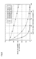
- the tendency observed from the result of measurement shown in Figs. 7A to 7D is similar to the result shown in Figs. 6A to 6D. It is noted, however, that the magnitude of the SN ratio tends to be larger in case of semiconductor laser devices (Figs. 7A to 7D).
- Fig. 8 represents the maximum SN ratio obtained when the thicknesses of the p and i layers of the light receiving element are optimized in accordance with the wavelength. From Fig. 8, it is understood that even when the light receiving element is improved, that is, optimized, the maximum SN ratio is about 150 in case of the LED. More specifically, when an LED is used, it is impossible to exceed the minimum SN ratio of about 150 that can be attained when a semiconductor laser device having the oscillation wavelengths of 885 to 980 nm is used.
- the wavelength band corresponds to the range of the absorption coefficient of 0.007 to 0.04 ⁇ m -1 for silicon, from Fig. 4.
- the optimal condition for the thickness of respective layers forming the light receiving element is that p layer is 5 to 25 ⁇ m and i layer is 60 to 200 ⁇ m.
- the laser beam can be taken out vertical to the circuit board, as already described.
- a method has also been tried in which the light beam is reflected by a side surface of a recessed portion formed in the circuit board 6 to take the light beam at the upper surface side. Satisfactory radiation pattern could not be obtained, however, as smoothness of the side surface of the recessed portion was insufficient.
- a laser mount that takes out the laser beam vertical to the circuit board as described above, satisfactory radiation pattern can be obtained, and an SN ratio larger than that of the LED can be attained.
- thermal resistance is 250 deg/W.
- the thermal resistance can be reduced to about 1/3, that is, 80 deg/W.
- Silicon resin 9 used for covering laser chip 1 described above is a so-called jellied resin, which has JISA hardness after curing of 0. Some rubber like resin materials having JISA hardness larger than 0 were tried. It was confirmed, however, that highest reliability is attained when a jellied resin is used.
- the oscillation wavelength of semiconductor laser device 1 is set to 930 nm.
- the oscillation wavelength of laser chip 1 can be adjusted by adjusting the ratio of mixed crystal of active layer InGaAs.
- As the light receiving element a light receiving element of an InP based compound semiconductor was used.
- the thickness of the p layer and the thickness of the i layer of the light receiving element was set to 3 ⁇ m and 15 ⁇ m.
- the SN ratio was measured under the same condition as the first embodiment, and the obtained SN ratio was 400.
- a light beam having the wavelength around 930 nm has absorption coefficient of about 0.07 ⁇ m -1 in the InP light receiving element 2.
- the absorption coefficient for the light beam having the wavelength of 900 nm is about 1.0 ⁇ m -1 .
- the absorption coefficient for the light beam of longer wavelength side for example, having the wavelength of 950 nm, is 0.0005 ⁇ m -1 . From these absorption coefficients and the equation (1), the ratio of surviving photons at a prescribed depth of the light incident on InP can be found.
- Fig. 9 represents the ratio of surviving photons with respect to the number of incident photons, when the light enters the InP light receiving element 2, where absorption coefficients are 1.0 (wavelength 900 nm), 0.07 (wavelength 930 nm), and 0.0005 ⁇ m -1 (wavelength 950 nm). It can be seen from Fig. 9 that the light beam having the wavelength of 910 nm or shorter is mostly absorbed only by the uppermost p layer 33, and an effective electric signal cannot be taken out therefrom. Namely, it does not form even a noise. The light beam having the wavelength of 940 nm or longer is not much absorbed, and hence the light is passed through p layer 33 and i layer 32, and hence it does not cause much noise, either.
- the wavelength range of the light that can be received by the above described light receiving element and that can be turned to the electric signal is about 900 to 950 nm.
- the InP light receiving element can be considered having an additional function of an optical filter having the wavelength range width of 50 nm.
- the inventor prepared semiconductor laser devices and LEDs as in the first embodiment, and signal to noise ratio (SN ratio) at the time of reception by the InP light receiving element was measured.
- the peak wavelength of the laser devices and the LEDs was changed in the range of 860 to 1020 nm.
- the results of measurement of the LEDs and the semiconductor laser devices are represented in Figs. 10A to 10D and 11A to 11D, respectively.
- the SN ratio begins to increase simultaneously as the wavelength is increased, the SN ratio increases abruptly when the wavelength exceeds 920 nm, and exhibits a peak near the wavelength of 940 nm. It is confirmed through experiment that when the wavelength is made still longer, the SN ratio abruptly degrades after 950 nm. By contrast, when the LED is used, the SN ratio tends to increase monotonously, as the peak wavelength is made longer.
- Fig. 12 represents the SN ratio when the layer thickness of the light receiving element is optimized for respective wavelengths.
- the SN ratio of the semiconductor laser device is significantly larger than that of LED, in the wavelength range of 920 to 940 nm. It has been proved that when the InP based light receiving element is used as the light receiving element, an extremely high SN ratio that could not be obtained so far can be attained, if a semiconductor laser device is used as an emission light source and the wavelength is within the range of 920 to 940 nm.
- the desirable combinations of the p and i layer thicknesses are as follows.
- the maximum SN ratio can readily be attained.
- the oscillation wavelength of the laser device when the oscillation wavelength of the laser device is set to 900 to 945 nm, it is the transition region where the absorption coefficient changes significantly and the absorption coefficient for the peak wavelength is 0.001 ⁇ m -1 , it becomes possible to perform optical filtering, using the difference in absorption coefficient.
- an LED is used as the light source that is received by the light receiving element of such an InP based photodiode, even when the central wavelength is in the range of 900 to 945 nm, the emission is broad, the light out of the wavelength range of 900 to 945 nm does not result in any electric signal.
- the intensity of the electric signal obtained from the LED light is significantly smaller than the signal intensity obtained from a light source of a line spectrum-like narrow line width within the wavelength range of 900 to 945 nm emitted from a semiconductor laser device.
- the noise comes from the background light, the noise is the same for both examples. Therefore, SN ratio of the LED is significantly smaller.
- the large difference in SN ratio between LED and the LD is based on the assumption that the oscillation wavelength of the LD is in the range of 900 to 945 nm. This wavelength range includes the absorption coefficient of 0.001 to 0.3 ⁇ m -1 , from the relation between the wavelength and absorption coefficient of InP shown in Fig. 4.
- the absorption coefficient of the light receiving element differs significantly, dependent on the material forming the light receiving element, as can be seen from Fig. 4.
- a direct transition type photodiode such as InP has a sharp absorption end, and is suitable for such a use as described in the present embodiment.
- a Ge photodiode has a sharp absorption end, and therefore, it can be used in the manner similar to InP.
- Fig. 15 represents SN ratios of the PD structures optimized for respective peak wavelengths. As the change rate of the absorption coefficient is moderate for Ge as compared with InP, even when an LED is used, the SN ratio does not decrease monotonously simultaneously with the increase of the wavelength, and it has a peak at about 1560 to 1580 nm, similar to a semiconductor laser device.
- the oscillation wavelength of the laser device should be 1.55 to 1.59 ⁇ m (1550 to 1590 nm).
- the wavelength is shorter than 1.55 ⁇ m, the absorption by the p layer of the light receiving element is too large, so that most of the light is absorbed before it enters the i layer, and hence the light does not contribute to any signal.
- the wavelength becomes longer than 1.59 ⁇ m, the light is not substantially absorbed either by the p layer or i layer but is passed therethrough, and hence the signal does not contribute to any signal, either.
- the wavelength range mentioned above is, similarly, correspond to the absorption coefficient of 0.001 to 0.06 ⁇ m -1 , from Fig. 4.
- the laser beam in the wavelength band of 1.55 ⁇ m can be oscillated by an InP based laser device, or a GaInNAs based laser device.
- the width of the wavelength range in which the absorption coefficient changes steeply over three to four orders is about 50 nm.
- the light source of which wavelength expansion is 50 nm or smaller is used in the wavelength range, it is possible to significantly improve the SN ratio.
- a light source of which wavelength expansion is at most 50 nm can be realized by the semiconductor laser device (LD) and not by an LED.
- the noise can significantly be reduced as compared with the conventional optical communication using an LED. Further, communication is possible between the optical transmitting/receiving apparatus and the conventional optical transmitting/receiving apparatus or an optical module formed of an Si light receiving element.
- a structure using a semiconductor laser having the wavelength of 1550 nm and a Ge light receiving element has higher safety with respect to one's eyes, as the wavelength is longer, and hence, it is possible to increase the optical output. This is as described in IEC60825-1, which is an international standardization reference.
- Both the InP light receiving element and the Ge light receiving element can be applied to a light source having the wavelength width of at most 50 nm.
- a light source having narrow width range industrially, a semiconductor laser device is most preferable.
- the light emitting diode has too wide an emission width, and as the wavelength other than the range mentioned above does not contribute to any signal, the SN ratio degrades abruptly.
- a semiconductor laser and a photodiode having light receiving sensitivity for a narrow band are used as in the present embodiment, it becomes unnecessary to provide an optical filter, and hence an optical transmitting/receiving apparatus can be formed at a low cost.
- Fig. 16 shows a semiconductor laser device (laser chip) in accordance with the third embodiment of the present invention. Referring to Fig. 16, the steps of forming the semiconductor laser device will be described. On an n type GaAs substrate 41, the layers having the following compositions and thicknesses are stacked in order from the lower side. The numerical values in the parentheses following the names of the layers represent the thickness of the layer.
- the portion up to the Al 0.1 GaAs second guide layer 49 serves as an active layer that causes laser oscillation at the wavelength of 920 nm.
- a p type Al 0.5 GaAs third clad layer 50 (3 ⁇ m) and thereafter a p type As contact layer 51 (2 ⁇ m) are stacked.
- a photomask is formed on the p type GaAs contact layer 51 through a common photo process.
- the direction of the waveguide is adapted to be in the ⁇ 110 > direction.
- GaAs contact layer 51 is etched.
- a hydrofluoric acid based etchant the third clad layer 50, active layer 49, 48, 47, 46 and 45 as well as the second clad layer 44 are etched. The etching automatically stops at the etching stopper layer 43.
- the sulfuric acid based etchant does not have plane direction dependency, and hence results in an almost vertical etching surface.
- the hydrofluoric acid based etchant has a plane direction dependency, and therefore, at the surface vertical to the direction of the waveguide, a ⁇ 111 ⁇ A plane is exposed, and an angle formed with the direction of the waveguide is about 54.7 degrees.
- the side surface of the waveguide may have a quasi mesa structure or anti mesa structure, dependent on the etching condition. Further, an almost vertical plane may be formed as shown in the figure.
- An SiN film 52 is embedded on the side surface of the waveguide, so that an upper part of the electrode contact layer 51 protrudes from the embedded layer.
- a metal electrode, not shown, is deposited on the upper surface, thus providing a positive electrode.
- Transparent electrode material, not shown, is provided on the lower surface, thus providing a negative electrode.
- one side is cleaved at a portion where the waveguide is disconnected, to form a surface 54. Thereafter, on the side of the surface 54, a highly reflective film of TiO 2 S i O 2 or the like is formed by vacuum vapor deposition.
- the active layer is so designed as to attain the laser oscillation wavelength of 920 nm.
- Fig. 17 shows energy (wavelength) dependency of the absorption coefficient of the n type GaAs.
- an n type GaAs substrate with the dosage of 2 to 4 ⁇ 10 18 cm -3 is used.
- the absorption coefficient is at most 10 cm -1 .
- the absorption coefficient is about 30 cm -1 , transmittance of at least 70% can be ensured for the GaAs substrate having the thickness of 100 ⁇ m. Therefore, when the optical energy is about 1.39eV, that is, when the wavelength is about 890 nm or longer, the effect of the present invention of the laser chip is attained.
- Fig. 18 shows only a data transmitting portion (light emitting portion) of a spatial optical transmission module.
- semiconductor laser device 1 is mounted on circuit board 6 with the positive electrode (not shown) facing downward.
- a silver paste not shown, is applied by an appropriate amount to circuit board 6, semiconductor laser device 1 is adhered, and cured at 80°C for a few minutes.
- the negative electrode (not shown) of the semiconductor laser device is connected by a wire 7a to an electrode (not shown) of circuit board 6.
- An upper portion of the semiconductor laser device is molded by a transparent resin 3 to which a diffuser 11 for diffusing light has been mixed, and by the same resin, a mold lens 4 is formed.
- the light reflected from the waveguide is propagated through resin 3, and the center of progress thereof is slightly deviated from the angle from the above.
- the mold lens of the present example is designed such that the light entering from above is focused on a reflecting surface of semiconductor laser device 1. Therefore, the optical beam that is in the opposite direction, that is, emitted obliquely from the vicinity of the focal point, is radiated to the space above. At this time, as there is the diffuser, the beam radiated to the space actually comes to be a beam having a certain expansion upward.
- the angle of expansion is determined by the density of the diffuser, and the expansion angle is the same both in the longitudinal and lateral directions.
- Such emission and entrance of light is preferred for a light emitting portion of the optical transmitting/receiving module.
- a light receiving element described with respect to the first embodiment is used.
- the semiconductor laser device of the present embodiment and the light receiving element of InP described with reference to the second embodiment are used, it becomes unnecessary to use a mold resin for optical filter, such as a black carbon, as already described in the second embodiment. Therefore, in the present example, for better design, an opaque resin with diffuser is used as the mold resin.
- the semiconductor laser device of the present embodiment By using the semiconductor laser device of the present embodiment, it becomes possible to take out the laser beam emitted upward from the upper surface, without using a special heat sink. Further, as the GaAs substrate has lower thermal conductivity as compared with metal, it is desired that the distance between the laser emitting portion, as a main heat generating portion, and the circuit board 6 is short. In the present example, absorption by the GaAs substrate can be minimized, by setting the wavelength to be 890 nm or longer. Thus, die-bonding of the laser emitting portion facing downward to the circuit board 6, that is, a so-called junction down type device mounting becomes possible.
- the thickness of SiN embedded film is about 20 ⁇ m in the semiconductor laser device 1 of the present example, which film covers a side surface of the pn junction. Therefore, even when silver paste 10 used at the time of die-bonding climbs up, leakage of current can be prevented when the climbing is at most 20 ⁇ m. Further, the optical filter becomes unnecessary, allowing selection of a mold resin. Further, the SiN film has a function of protecting an end surface, and therefore, a highly reliable laser chip can be realized by a simple method.
- Fig. 20 is a perspective view showing a mini disk player 60 mounting the spatial optical transmission module 62 in accordance with the third embodiment of the present invention and a remote controller 61.
- Mini disk player 60 has the entire surface finished with silver aluminum.
- the mold resin in accordance with the third embodiment is opaque, and hence good color balance with the silver case can be attained, thus improving the value of the overall system as a product.
- the present embodiment provides an optical transmitting/receiving module that matches the color of the product, for improved design. Further, by the use of the spatial optical transmission system of the present invention, it becomes possible for the first time to provide a transparent mold resin.
Landscapes
- Physics & Mathematics (AREA)
- Engineering & Computer Science (AREA)
- Optics & Photonics (AREA)
- Electromagnetism (AREA)
- Nanotechnology (AREA)
- Chemical & Material Sciences (AREA)
- Signal Processing (AREA)
- Biophysics (AREA)
- Life Sciences & Earth Sciences (AREA)
- Crystallography & Structural Chemistry (AREA)
- Computer Networks & Wireless Communication (AREA)
- Condensed Matter Physics & Semiconductors (AREA)
- General Physics & Mathematics (AREA)
- Light Receiving Elements (AREA)
- Semiconductor Lasers (AREA)
- Optical Communication System (AREA)
- Photo Coupler, Interrupter, Optical-To-Optical Conversion Devices (AREA)
Priority Applications (1)
| Application Number | Priority Date | Filing Date | Title |
|---|---|---|---|
| EP06005995A EP1681751A1 (en) | 2001-04-20 | 2002-04-18 | Semiconductor laser module, spatial optical transmission system and electronic appliance |
Applications Claiming Priority (4)
| Application Number | Priority Date | Filing Date | Title |
|---|---|---|---|
| JP2001122399 | 2001-04-20 | ||
| JP2001122399 | 2001-04-20 | ||
| JP2002026725A JP4097949B2 (ja) | 2001-04-20 | 2002-02-04 | 空間光伝送システム |
| JP2002026725 | 2002-02-04 |
Related Child Applications (1)
| Application Number | Title | Priority Date | Filing Date |
|---|---|---|---|
| EP06005995A Division EP1681751A1 (en) | 2001-04-20 | 2002-04-18 | Semiconductor laser module, spatial optical transmission system and electronic appliance |
Publications (3)
| Publication Number | Publication Date |
|---|---|
| EP1251607A2 EP1251607A2 (en) | 2002-10-23 |
| EP1251607A3 EP1251607A3 (en) | 2003-05-07 |
| EP1251607B1 true EP1251607B1 (en) | 2006-05-17 |
Family
ID=26613908
Family Applications (2)
| Application Number | Title | Priority Date | Filing Date |
|---|---|---|---|
| EP02252736A Expired - Lifetime EP1251607B1 (en) | 2001-04-20 | 2002-04-18 | Semiconductor laser module, spatial optical transmission system and electronic appliance |
| EP06005995A Ceased EP1681751A1 (en) | 2001-04-20 | 2002-04-18 | Semiconductor laser module, spatial optical transmission system and electronic appliance |
Family Applications After (1)
| Application Number | Title | Priority Date | Filing Date |
|---|---|---|---|
| EP06005995A Ceased EP1681751A1 (en) | 2001-04-20 | 2002-04-18 | Semiconductor laser module, spatial optical transmission system and electronic appliance |
Country Status (4)
| Country | Link |
|---|---|
| US (2) | US6970489B2 (https=) |
| EP (2) | EP1251607B1 (https=) |
| JP (1) | JP4097949B2 (https=) |
| DE (1) | DE60211414T2 (https=) |
Families Citing this family (22)
| Publication number | Priority date | Publication date | Assignee | Title |
|---|---|---|---|---|
| US6712529B2 (en) * | 2000-12-11 | 2004-03-30 | Rohm Co., Ltd. | Infrared data communication module and method of making the same |
| US7061025B2 (en) * | 2003-03-10 | 2006-06-13 | Mccolloch Lawrence R | Optoelectronic device packaging assemblies and methods of making the same |
| US7508854B2 (en) * | 2003-11-14 | 2009-03-24 | Sanyo Electric Co., Ltd. | Semiconductor laser device |
| JP3857694B2 (ja) * | 2004-02-05 | 2006-12-13 | ローム株式会社 | 光通信モジュール |
| KR100945621B1 (ko) * | 2005-03-07 | 2010-03-04 | 로무 가부시키가이샤 | 광 통신 모듈 및 그 제조 방법 |
| JP4969055B2 (ja) * | 2005-04-28 | 2012-07-04 | ローム株式会社 | 光通信モジュール |
| US7482666B2 (en) * | 2006-01-12 | 2009-01-27 | Silicon Laboratories Inc. | Apparatus and method for optical isolation |
| JP2007258667A (ja) * | 2006-02-21 | 2007-10-04 | Seiko Epson Corp | 光電気複合基板及び電子機器 |
| JP5114773B2 (ja) * | 2007-08-10 | 2013-01-09 | スタンレー電気株式会社 | 表面実装型発光装置 |
| EP2249201A4 (en) | 2008-03-03 | 2011-08-10 | Sharp Kk | DISPLAY DEVICE WITH LIGHT SENSOR |
| US20130223846A1 (en) | 2009-02-17 | 2013-08-29 | Trilumina Corporation | High speed free-space optical communications |
| US9620934B2 (en) * | 2010-08-31 | 2017-04-11 | Avago Technologies General Ip (Singapore) Pte. Ltd. | Flip-chip assembly comprising an array of vertical cavity surface emitting lasers (VCSELs) |
| US9188751B2 (en) | 2010-08-31 | 2015-11-17 | Avago Technologies General Ip (Singapore) Pte. Ltd. | Flip-chip assembly comprising an array of vertical cavity surface emitting lasers (VCSELSs), and an optical transmitter assembly that incorporates the flip-chip assembly |
| WO2012115246A1 (ja) * | 2011-02-25 | 2012-08-30 | ローム株式会社 | 通信モジュールおよび携帯型電子機器 |
| US11095365B2 (en) * | 2011-08-26 | 2021-08-17 | Lumentum Operations Llc | Wide-angle illuminator module |
| US20150270900A1 (en) * | 2014-03-19 | 2015-09-24 | Apple Inc. | Optical data transfer utilizing lens isolation |
| KR102378761B1 (ko) * | 2015-07-21 | 2022-03-25 | 엘지이노텍 주식회사 | 일체형 발광 패키지 및 이를 이용한 차량용 램프 |
| US10539661B2 (en) * | 2015-11-25 | 2020-01-21 | Velodyne Lidar, Inc. | Three dimensional LIDAR system with targeted field of view |
| JP6940749B2 (ja) * | 2016-04-28 | 2021-09-29 | 日亜化学工業株式会社 | 発光装置 |
| US10148365B2 (en) * | 2017-01-05 | 2018-12-04 | Intel Corporation | Hybrid free air and electrical interconnect |
| CN114069378B (zh) * | 2020-07-30 | 2025-07-22 | 核工业理化工程研究院 | 一种高功率激光长距离传输装置及其长距离传输方法 |
| DE102022201340A1 (de) * | 2022-02-09 | 2023-08-24 | Osram Opto Semiconductors Gmbh | Halbleiterlaser mit Strahlungsführungselement |
Family Cites Families (31)
| Publication number | Priority date | Publication date | Assignee | Title |
|---|---|---|---|---|
| DE2737345C2 (de) * | 1976-08-20 | 1991-07-25 | Canon K.K., Tokio/Tokyo | Halbleiterlaser-Vorrichtung mit einem Peltier-Element |
| JPS5848443A (ja) * | 1981-09-17 | 1983-03-22 | Toshiba Corp | 樹脂封止型半導体装置 |
| JPS6063977A (ja) * | 1983-09-17 | 1985-04-12 | Mitsubishi Electric Corp | 半導体レ−ザ装置 |
| JPS60154689A (ja) * | 1984-01-25 | 1985-08-14 | Hitachi Ltd | 発光素子およびこれを用いた光通信装置 |
| KR910004265B1 (ko) * | 1987-03-26 | 1991-06-25 | 가부시기가이샤 히다찌세이사꾸쇼 | 반도체 레이저 장치와 그 제조 방법 및 그것을 사용한 광 헤드 |
| US5130563A (en) * | 1989-11-30 | 1992-07-14 | Washington Research Foundation | Optoelectronic sensory neural network |
| JPH03274781A (ja) * | 1990-03-23 | 1991-12-05 | Rohm Co Ltd | レーザダイオード |
| US5140384A (en) * | 1990-06-14 | 1992-08-18 | Rohm Co., Ltd. | Semiconductor laser device mounted on a stem |
| JPH0448674A (ja) * | 1990-06-14 | 1992-02-18 | Rohm Co Ltd | 半導体レーザ |
| JPH04144396A (ja) * | 1990-10-04 | 1992-05-18 | Sony Corp | 双方向リモートコントロール装置 |
| US5590144A (en) * | 1990-11-07 | 1996-12-31 | Fuji Electric Co., Ltd. | Semiconductor laser device |
| JPH04216682A (ja) * | 1990-12-18 | 1992-08-06 | Sumitomo Electric Ind Ltd | 受光素子 |
| JPH06252856A (ja) * | 1992-12-30 | 1994-09-09 | Canon Inc | 近赤外光空間通信装置 |
| US5680241A (en) * | 1992-12-30 | 1997-10-21 | Canon Kabushiki Kaisha | Optical space communication |
| JP3110586B2 (ja) * | 1993-06-04 | 2000-11-20 | 松下電子工業株式会社 | 半導体レーザ装置 |
| EP0632511A3 (en) * | 1993-06-29 | 1996-11-27 | Mitsubishi Cable Ind Ltd | Light emitting diode assembly and manufacturing method. |
| IL114176A (en) * | 1995-06-15 | 2000-02-29 | Jolt Ltd | Wireless communication system |
| JPH09252285A (ja) * | 1996-03-15 | 1997-09-22 | Toshiba Corp | 近赤外線通信装置 |
| JPH10190584A (ja) | 1996-10-25 | 1998-07-21 | Seiko Epson Corp | 光無線データ通信システムと、それに用いる送信装置、受信装置 |
| US6310707B1 (en) * | 1996-10-25 | 2001-10-30 | Seiko Epson Corporation | Optical wireless data communication system, and transmitter and receiver used therefor |
| JP3425310B2 (ja) * | 1996-11-25 | 2003-07-14 | シャープ株式会社 | 発光/受光装置 |
| JP3087676B2 (ja) * | 1997-02-13 | 2000-09-11 | 日本電気株式会社 | ゲル状樹脂を用いた光結合系及び実装構造 |
| US5844257A (en) * | 1997-06-12 | 1998-12-01 | Quarton, Inc. | Multi-directional light emitting semiconductor device |
| JP3948789B2 (ja) * | 1997-07-02 | 2007-07-25 | シチズン電子株式会社 | 赤外線データ通信モジュール |
| US6020590A (en) * | 1998-01-22 | 2000-02-01 | Ois Optical Imaging Systems, Inc. | Large area imager with UV blocking layer |
| US6081020A (en) * | 1998-02-20 | 2000-06-27 | Lucent Technologies Inc. | Linear PIN photodiode |
| EP1079550B1 (en) * | 1998-04-24 | 2007-10-31 | Sharp Kabushiki Kaisha | Space-division multiplex full-duplex local area network |
| US6452669B1 (en) * | 1998-08-31 | 2002-09-17 | Digital Optics Corp. | Transmission detection for vertical cavity surface emitting laser power monitor and system |
| US6198800B1 (en) * | 1998-09-16 | 2001-03-06 | Canon Kabushiki Kaisha | Exposure control for digital radiography systems using charge build-up in sensor array pixels |
| EP1163711A1 (en) * | 1999-03-24 | 2001-12-19 | Cielo Communications, Inc. | Encapsulated optoelectronic devices with controlled properties |
| JP4902044B2 (ja) * | 1999-09-24 | 2012-03-21 | シャープ株式会社 | 半導体レーザ装置、光伝送装置、光伝送システム、電子機器、制御装置、接続コネクタ、通信装置、ならびに光伝送方法、データ送受信方法 |
-
2002
- 2002-02-04 JP JP2002026725A patent/JP4097949B2/ja not_active Expired - Fee Related
- 2002-04-18 EP EP02252736A patent/EP1251607B1/en not_active Expired - Lifetime
- 2002-04-18 DE DE60211414T patent/DE60211414T2/de not_active Expired - Lifetime
- 2002-04-18 EP EP06005995A patent/EP1681751A1/en not_active Ceased
- 2002-04-22 US US10/126,967 patent/US6970489B2/en not_active Expired - Lifetime
-
2005
- 2005-09-20 US US11/229,618 patent/US20060062269A1/en not_active Abandoned
Also Published As
| Publication number | Publication date |
|---|---|
| JP4097949B2 (ja) | 2008-06-11 |
| US20060062269A1 (en) | 2006-03-23 |
| JP2003008131A (ja) | 2003-01-10 |
| EP1681751A1 (en) | 2006-07-19 |
| EP1251607A2 (en) | 2002-10-23 |
| DE60211414T2 (de) | 2007-04-26 |
| US6970489B2 (en) | 2005-11-29 |
| DE60211414D1 (de) | 2006-06-22 |
| US20020154667A1 (en) | 2002-10-24 |
| EP1251607A3 (en) | 2003-05-07 |
Similar Documents
| Publication | Publication Date | Title |
|---|---|---|
| EP1251607B1 (en) | Semiconductor laser module, spatial optical transmission system and electronic appliance | |
| US6005262A (en) | Flip-chip bonded VCSEL CMOS circuit with silicon monitor detector | |
| US6037644A (en) | Semi-transparent monitor detector for surface emitting light emitting devices | |
| US20060124946A1 (en) | Optical transmitter | |
| US7085300B2 (en) | Integral vertical cavity surface emitting laser and power monitor | |
| US6593602B2 (en) | Edge emission type semiconductor device for emitting super luminescent light, its manufacture and spatial optical communication device | |
| KR100532281B1 (ko) | 면굴절 입사형 수광소자 및 그 제조방법 | |
| JPH09214066A (ja) | 一体化レーザ・ベース光源 | |
| US6847053B2 (en) | Optical transmitter | |
| US6973110B2 (en) | Monolithic laser configuration | |
| JPH02191389A (ja) | 半導体レーザ装置 | |
| US7465960B2 (en) | Submount for light emitting/receiving device | |
| JP5197978B2 (ja) | 光半導体モジュール | |
| KR100464333B1 (ko) | 수광소자 및 그 제조방법 | |
| KR102761471B1 (ko) | 표면방출발광레이저 패키지 및 이를 포함하는 광 모듈 | |
| US7057255B2 (en) | Photodiode, optical receiver device including the same, and method of making the photodiode | |
| US20030122061A1 (en) | Optical device, optical device module and carrier for optical device | |
| TWI782350B (zh) | 光模態轉換裝置及其製造方法 | |
| US20040141699A1 (en) | Optical module | |
| US6807326B2 (en) | Optical module for suppressing optical and electrical crosstalk simultaneously | |
| US7620090B2 (en) | Semiconductor laser device | |
| JP3320058B2 (ja) | アングルキャビティ共鳴型光検出器組立体及びその製造方法 | |
| JP2004241746A (ja) | 高速受光素子およびその製造方法 | |
| JP3272060B2 (ja) | 半導体素子 | |
| JP2000183439A (ja) | 半導体レーザ装置 |
Legal Events
| Date | Code | Title | Description |
|---|---|---|---|
| PUAI | Public reference made under article 153(3) epc to a published international application that has entered the european phase |
Free format text: ORIGINAL CODE: 0009012 |
|
| AK | Designated contracting states |
Kind code of ref document: A2 Designated state(s): AT BE CH CY DE DK ES FI FR GB GR IE IT LI LU MC NL PT SE TR |
|
| AX | Request for extension of the european patent |
Free format text: AL;LT;LV;MK;RO;SI |
|
| PUAL | Search report despatched |
Free format text: ORIGINAL CODE: 0009013 |
|
| AK | Designated contracting states |
Designated state(s): AT BE CH CY DE DK ES FI FR GB GR IE IT LI LU MC NL PT SE TR |
|
| AX | Request for extension of the european patent |
Extension state: AL LT LV MK RO SI |
|
| 17P | Request for examination filed |
Effective date: 20030723 |
|
| 17Q | First examination report despatched |
Effective date: 20030903 |
|
| AKX | Designation fees paid |
Designated state(s): DE FR GB |
|
| GRAP | Despatch of communication of intention to grant a patent |
Free format text: ORIGINAL CODE: EPIDOSNIGR1 |
|
| GRAS | Grant fee paid |
Free format text: ORIGINAL CODE: EPIDOSNIGR3 |
|
| GRAA | (expected) grant |
Free format text: ORIGINAL CODE: 0009210 |
|
| AK | Designated contracting states |
Kind code of ref document: B1 Designated state(s): DE FR GB |
|
| REG | Reference to a national code |
Ref country code: GB Ref legal event code: FG4D |
|
| REF | Corresponds to: |
Ref document number: 60211414 Country of ref document: DE Date of ref document: 20060622 Kind code of ref document: P |
|
| ET | Fr: translation filed | ||
| PLBE | No opposition filed within time limit |
Free format text: ORIGINAL CODE: 0009261 |
|
| STAA | Information on the status of an ep patent application or granted ep patent |
Free format text: STATUS: NO OPPOSITION FILED WITHIN TIME LIMIT |
|
| 26N | No opposition filed |
Effective date: 20070220 |
|
| REG | Reference to a national code |
Ref country code: DE Ref legal event code: R084 Ref document number: 60211414 Country of ref document: DE |
|
| REG | Reference to a national code |
Ref country code: GB Ref legal event code: 746 Effective date: 20140918 |
|
| REG | Reference to a national code |
Ref country code: DE Ref legal event code: R084 Ref document number: 60211414 Country of ref document: DE Effective date: 20141002 |
|
| REG | Reference to a national code |
Ref country code: FR Ref legal event code: PLFP Year of fee payment: 15 |
|
| REG | Reference to a national code |
Ref country code: FR Ref legal event code: PLFP Year of fee payment: 16 |
|
| REG | Reference to a national code |
Ref country code: FR Ref legal event code: PLFP Year of fee payment: 17 |
|
| PGFP | Annual fee paid to national office [announced via postgrant information from national office to epo] |
Ref country code: FR Payment date: 20210818 Year of fee payment: 20 |
|
| PGFP | Annual fee paid to national office [announced via postgrant information from national office to epo] |
Ref country code: GB Payment date: 20210820 Year of fee payment: 20 Ref country code: DE Payment date: 20210819 Year of fee payment: 20 |
|
| REG | Reference to a national code |
Ref country code: DE Ref legal event code: R071 Ref document number: 60211414 Country of ref document: DE |
|
| REG | Reference to a national code |
Ref country code: GB Ref legal event code: PE20 Expiry date: 20220417 |
|
| PG25 | Lapsed in a contracting state [announced via postgrant information from national office to epo] |
Ref country code: GB Free format text: LAPSE BECAUSE OF EXPIRATION OF PROTECTION Effective date: 20220417 |