EP1213757A2 - Integrierte Schaltkreise und benachbarte p-dotierte Gebiete mit flachen Grabenisolations-Strukturen ohne "Liner"-Schichten dazwischen und zugeörige Herstellungsverfahren - Google Patents
Integrierte Schaltkreise und benachbarte p-dotierte Gebiete mit flachen Grabenisolations-Strukturen ohne "Liner"-Schichten dazwischen und zugeörige Herstellungsverfahren Download PDFInfo
- Publication number
- EP1213757A2 EP1213757A2 EP01128854A EP01128854A EP1213757A2 EP 1213757 A2 EP1213757 A2 EP 1213757A2 EP 01128854 A EP01128854 A EP 01128854A EP 01128854 A EP01128854 A EP 01128854A EP 1213757 A2 EP1213757 A2 EP 1213757A2
- Authority
- EP
- European Patent Office
- Prior art keywords
- integrated circuit
- trench
- layer
- forming
- side wall
- Prior art date
- Legal status (The legal status is an assumption and is not a legal conclusion. Google has not performed a legal analysis and makes no representation as to the accuracy of the status listed.)
- Granted
Links
- 238000000034 method Methods 0.000 title claims description 38
- 238000002955 isolation Methods 0.000 title claims description 21
- 239000000758 substrate Substances 0.000 claims abstract description 79
- 239000012212 insulator Substances 0.000 claims abstract description 30
- 230000002093 peripheral effect Effects 0.000 claims description 54
- 239000004065 semiconductor Substances 0.000 claims description 39
- 229910052581 Si3N4 Inorganic materials 0.000 claims description 26
- HQVNEWCFYHHQES-UHFFFAOYSA-N silicon nitride Chemical compound N12[Si]34N5[Si]62N3[Si]51N64 HQVNEWCFYHHQES-UHFFFAOYSA-N 0.000 claims description 26
- 239000003989 dielectric material Substances 0.000 claims description 21
- XUIMIQQOPSSXEZ-UHFFFAOYSA-N Silicon Chemical compound [Si] XUIMIQQOPSSXEZ-UHFFFAOYSA-N 0.000 claims description 11
- 230000000903 blocking effect Effects 0.000 claims description 11
- 229910052710 silicon Inorganic materials 0.000 claims description 11
- 239000010703 silicon Substances 0.000 claims description 11
- 238000005530 etching Methods 0.000 claims description 5
- 238000004519 manufacturing process Methods 0.000 claims description 3
- 230000001590 oxidative effect Effects 0.000 claims description 3
- 238000005498 polishing Methods 0.000 claims description 3
- 238000000059 patterning Methods 0.000 claims 3
- 238000000151 deposition Methods 0.000 claims 2
- 238000001312 dry etching Methods 0.000 description 6
- 230000007547 defect Effects 0.000 description 5
- 238000000206 photolithography Methods 0.000 description 5
- 239000000969 carrier Substances 0.000 description 3
- 229920002120 photoresistant polymer Polymers 0.000 description 3
- 241000293849 Cordylanthus Species 0.000 description 2
- NBIIXXVUZAFLBC-UHFFFAOYSA-N Phosphoric acid Chemical compound OP(O)(O)=O NBIIXXVUZAFLBC-UHFFFAOYSA-N 0.000 description 2
- VYPSYNLAJGMNEJ-UHFFFAOYSA-N Silicium dioxide Chemical compound O=[Si]=O VYPSYNLAJGMNEJ-UHFFFAOYSA-N 0.000 description 2
- 230000015572 biosynthetic process Effects 0.000 description 2
- 230000015556 catabolic process Effects 0.000 description 2
- 230000000694 effects Effects 0.000 description 2
- 229910052814 silicon oxide Inorganic materials 0.000 description 2
- 230000002411 adverse Effects 0.000 description 1
- 229910000147 aluminium phosphate Inorganic materials 0.000 description 1
- 238000000280 densification Methods 0.000 description 1
- 230000005669 field effect Effects 0.000 description 1
- 239000012535 impurity Substances 0.000 description 1
- 230000010354 integration Effects 0.000 description 1
- 229910044991 metal oxide Inorganic materials 0.000 description 1
- 150000004706 metal oxides Chemical class 0.000 description 1
- 230000003647 oxidation Effects 0.000 description 1
- 238000007254 oxidation reaction Methods 0.000 description 1
- 230000035515 penetration Effects 0.000 description 1
- 239000000126 substance Substances 0.000 description 1
- 238000001039 wet etching Methods 0.000 description 1
Images


Classifications
-
- H—ELECTRICITY
- H01—ELECTRIC ELEMENTS
- H01L—SEMICONDUCTOR DEVICES NOT COVERED BY CLASS H10
- H01L21/00—Processes or apparatus adapted for the manufacture or treatment of semiconductor or solid state devices or of parts thereof
- H01L21/70—Manufacture or treatment of devices consisting of a plurality of solid state components formed in or on a common substrate or of parts thereof; Manufacture of integrated circuit devices or of parts thereof
- H01L21/71—Manufacture of specific parts of devices defined in group H01L21/70
- H01L21/76—Making of isolation regions between components
- H01L21/762—Dielectric regions, e.g. EPIC dielectric isolation, LOCOS; Trench refilling techniques, SOI technology, use of channel stoppers
- H01L21/76224—Dielectric regions, e.g. EPIC dielectric isolation, LOCOS; Trench refilling techniques, SOI technology, use of channel stoppers using trench refilling with dielectric materials
- H01L21/76229—Concurrent filling of a plurality of trenches having a different trench shape or dimension, e.g. rectangular and V-shaped trenches, wide and narrow trenches, shallow and deep trenches
-
- H—ELECTRICITY
- H01—ELECTRIC ELEMENTS
- H01L—SEMICONDUCTOR DEVICES NOT COVERED BY CLASS H10
- H01L21/00—Processes or apparatus adapted for the manufacture or treatment of semiconductor or solid state devices or of parts thereof
- H01L21/70—Manufacture or treatment of devices consisting of a plurality of solid state components formed in or on a common substrate or of parts thereof; Manufacture of integrated circuit devices or of parts thereof
- H01L21/71—Manufacture of specific parts of devices defined in group H01L21/70
- H01L21/76—Making of isolation regions between components
- H01L21/762—Dielectric regions, e.g. EPIC dielectric isolation, LOCOS; Trench refilling techniques, SOI technology, use of channel stoppers
- H01L21/76224—Dielectric regions, e.g. EPIC dielectric isolation, LOCOS; Trench refilling techniques, SOI technology, use of channel stoppers using trench refilling with dielectric materials
- H01L21/76232—Dielectric regions, e.g. EPIC dielectric isolation, LOCOS; Trench refilling techniques, SOI technology, use of channel stoppers using trench refilling with dielectric materials of trenches having a shape other than rectangular or V-shape, e.g. rounded corners, oblique or rounded trench walls
-
- H—ELECTRICITY
- H01—ELECTRIC ELEMENTS
- H01L—SEMICONDUCTOR DEVICES NOT COVERED BY CLASS H10
- H01L21/00—Processes or apparatus adapted for the manufacture or treatment of semiconductor or solid state devices or of parts thereof
- H01L21/70—Manufacture or treatment of devices consisting of a plurality of solid state components formed in or on a common substrate or of parts thereof; Manufacture of integrated circuit devices or of parts thereof
- H01L21/77—Manufacture or treatment of devices consisting of a plurality of solid state components or integrated circuits formed in, or on, a common substrate
- H01L21/78—Manufacture or treatment of devices consisting of a plurality of solid state components or integrated circuits formed in, or on, a common substrate with subsequent division of the substrate into plural individual devices
- H01L21/82—Manufacture or treatment of devices consisting of a plurality of solid state components or integrated circuits formed in, or on, a common substrate with subsequent division of the substrate into plural individual devices to produce devices, e.g. integrated circuits, each consisting of a plurality of components
- H01L21/822—Manufacture or treatment of devices consisting of a plurality of solid state components or integrated circuits formed in, or on, a common substrate with subsequent division of the substrate into plural individual devices to produce devices, e.g. integrated circuits, each consisting of a plurality of components the substrate being a semiconductor, using silicon technology
- H01L21/8232—Field-effect technology
- H01L21/8234—MIS technology, i.e. integration processes of field effect transistors of the conductor-insulator-semiconductor type
- H01L21/823481—MIS technology, i.e. integration processes of field effect transistors of the conductor-insulator-semiconductor type isolation region manufacturing related aspects, e.g. to avoid interaction of isolation region with adjacent structure
Definitions
- the present invention relates to integrated circuits and methods of forming integrated circuits in general and, more particularly, to shallow trench isolation structures in integrated circuits and methods of forming shallow trench isolation structures in integrated circuits.
- LOCOS Local Oxidation Of Silicon
- a semiconductor substrate 10 includes as a cell region, a core region and a peripheral region.
- a blocking pattern (not shown) is formed on the semiconductor substrate 10 to expose an isolation region.
- the blocking pattern may be a stack of an oxide layer and a silicon nitride layer.
- the exposed semiconductor substrate 10 is etched to a depth using the blocking pattern as a mask to form trenches t 1 and t 2 .
- the trench t 1 is formed in the cell region and the trench t 2 is used to define a PMOS transistor region in the core and peripheral regions.
- the trenches t 1 and t 2 can be formed by dry etching using plasma.
- the dry etching may cause silicon lattice defects and damage the inner surfaces of the trenches t 1 and t 2 .
- a side wall oxide layer 12 can be formed by thermally oxidizing the inner surfaces of the trenches t 1 and t 2 . Also, the formation of the side wall oxide layer 12 can remove sharp comers generated in the trenches t 1 and t 2 associated with the bird's beak effect discussed above.
- a silicon nitride liner 14 can be formed on the side wall oxide layer 12 .
- the silicon nitride liner 14 may reduce stress due to a difference between the respective thermal expansion coefficients associated with the semiconductor substrate 10 and a silicon oxide layer in the trenches t 1 and t 2 .
- a dielectric material such as a High Density Plasma (HDP) oxide
- HDP High Density Plasma
- CMP Chemical Mechanical Polishing
- the semiconductor device having the conventional STI structure discussed above may cause the following problems.
- high energy or "hot" carriers in a MOS transistor can penetrate through the side wall oxide layer 12 into the STI layer 16 .
- N-type charged carriers, such as electrons 30 that penetrate into the STI layer 16 may collect at an interface of the silicon nitride liner 14 and the side wall oxide layer 12 and in the silicon nitride liner 14 as shown in FIG. 2A.
- the electrons 30 may be trapped at the interface due the thickness of the side wall oxide layer 12 .
- positive holes 32 can be induced at a boundary of the STI layer 16 opposite the electrons 30 as shown in FIG. 2A.
- a conductive path through the semiconductor substrate 10 may not be formed between n-type junction regions 26a and 26b of an N-channel field effect transistor (N-FET) because the major carriers are electrons 30 .
- the holes 32 at the boundary of the STI layer 16 can provide a current path I that electrically connects a p-type junction region 28a (associated with a gate electrode of a Metal Oxide Semiconductor (MOSFET) 24 ) and 28b associated with an adjacent MOSFET.
- MOSFET Metal Oxide Semiconductor
- holes may be induced in the channel region of the P-FET thereby affecting the operation of the P-FET. Also, holes induced when the P-FET is turned on may not be easily removed and, therefore, may remain after the P-FET is turned off. The length of the channel of the P-FET may, therefore, be reduced which may decrease the threshold and breakdown voltages associated with the P-FET.
- Embodiments according to the present invention may provide integrated circuits having Shallow Trench Isolation (STI) structures.
- an integrated circuit substrate can include first and second adjacent p-type doped regions spaced-apart from one another in the integrated circuit substrate.
- a trench in the integrated circuit substrate is between the first and second adjacent p-type doped regions.
- An insulator layer in the trench has a side wall, wherein the side wall is free of a layer thereon that reduces a stress between the integrated circuit substrate and the insulator layer.
- a dielectric material is in the trench directly on the side wall.
- the trench is a first trench and the side wall is a first side wall and the insulator layer is a first insulator layer.
- First and second adjacent n-type doped regions are spaced-apart from one another in the integrated circuit substrate.
- a second trench is in the integrated circuit substrate between the first and second adjacent n-type doped regions.
- a second insulator layer in the second trench has a second side wall.
- a liner layer on the second side wall can reduce a stress between the integrated circuit substrate and the second insulator layer.
- the dielectric material is a first dielectric material and a second dielectric material is in the second trench on the liner layer.
- the side wall is free of silicon nitride.
- the integrated circuit includes a core region, a peripheral region, and a cell region that is spaced apart from the core and peripheral regions and has a greater density of integrated circuit devices therein than the core and peripheral regions, wherein the first trench is in one of the peripheral and core regions. The second trench is in the cell region.
- the integrated circuit includes a core region, a peripheral region, and a cell region that is spaced apart from the core and peripheral regions and has a greater density of integrated circuit devices therein than the core and peripheral regions.
- the trench is between the core and peripheral regions and the cell region.
- the integrated circuit includes a core region, a peripheral region, and a cell region that is spaced apart from the core and peripheral regions and has a greater density of integrated circuit devices therein than the core and peripheral regions.
- the trench is in one of the core and peripheral regions.
- first and second adjacent p-type doped regions are formed spaced-apart from one another in an integrated circuit substrate.
- a trench is formed in the integrated circuit substrate between the first and second adjacent p-type doped regions.
- An insulator layer is formed in the trench having a side wall, wherein the side wall is free of a layer that reduces a stress between the integrated circuit substrate and the insulator layer.
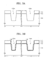
- a pad oxide layer 102 and a silicon nitride layer 104 are formed on a semiconductor substrate 100.
- the semiconductor substrate 100 which can be a silicon substrate containing impurities, is defined as having a cell region in which memory devices can be formed and core and peripheral regions in which PMOS transistors can be formed.
- A1 denotes the cell region and A2 denotes the core and peripheral regions.
- the pad oxide layer 102 is formed to a thickness in a range between about 70 and 160 ⁇ ngstroms and the silicon nitride layer 104 is formed in a range between about 1300 and 1600 ⁇ ngstroms.
- the silicon nitride layer 104 and the pad oxide layer 102 are etched using known photolithography processes, to expose a pre-isolation region of the semiconductor substrate 100 thereby forming a blocking pattern.
- pre-isolation region means a region for defining the cell, core and peripheral regions and the isolation structures formed in respective regions.
- the first and second trenches 106a and 106b are formed by etching the semiconductor substrate 100 to a depth in a range between about 0.1 and 1.5 ⁇ m and preferably to a depth in a range between about 0.24 and 0.26 ⁇ m using the blocking pattern as a mask.
- the first and second trenches 106a and 106b are used to form Shallow Trench Isolation (STI) structures.
- the first trench 106a can provide isolation between devices formed in the cell region A1 and the second trench 106b can provide isolation between devices formed in the core and peripheral regions A2.
- the first trench 106a is formed in the cell region A1 which may be densely populated with devices. Accordingly, the width of the first trench 106a may be less than the width of the second trench 106b that is formed in the core and peripheral regions A2.
- the first and second trenches 106a and 106b may be formed using dry etching in conjunction with a plasma. The dry etching may cause silicon lattice defects and damage to the surfaces of the first and second trenches 106a and 106b. For example, dry etching may cause the formation of sharp comers at the bottom of the side walls in the first and second trenches 106a and 106b.
- a side wall oxide layer 108 is formed in the first and second trenches 106a and 106b by thermally oxidizing the inner surfaces of the first and second trenches 106a and 106b.
- the side wall oxide layer 108 may address the silicon lattice defects and the damage to the first and second trenches 106a and 106b.
- the side wall oxide layer 108 may smooth the sharp comers at the bottom of the side walls of the first and second trenches 106a and 106b.
- the side wall oxide layer 108 is formed to a thickness in a range between about 20 and 240 ⁇ ngstroms and more preferably in a range between about 20 and 50 ⁇ ngstroms.
- a relief liner 110 is formed on the side wall oxide layer 108.
- the relief liner 110 may relieve a stress caused by a difference between the respective thermal expansion coefficients associated with the silicon semiconductor substrate 100 and a dielectric in the trenches 106a and 106b.
- the relief liner 110 may also reduce the penetration of defects into the first and second trenches 106a and 106b.
- the relief liner 110 is a silicon nitride layer or a silicon oxynitride layer either of which can be formed to a thickness in a range between about of 50 and 100 ⁇ ngstroms.
- a photoresist pattern 112 is formed on the cell region using a known photolithography process.
- the core and peripheral regions A2 are exposed.
- the relief liner 110 on the core and peripheral regions A2 is removed so that the side wall oxide layer 108 is free of the relief liner 110 thereon.
- it is preferable that the relief liner 110 is etched using isotropic etching.
- the isotropic etching is a wet etching using a phosphoric acid solution or a dry etching using an isotropic gas.
- the photoresist pattern 112 is removed by a known method.
- a dielectric layer 114 is formed on the resultant semiconductor substrate 100 to a thickness of more than about 6000 ⁇ ngstroms to fill the first and second trenches 106a and 106b.
- the dielectric layer 114 is a HDP dielectric layer having good filling properties.
- the dielectric layer 114 is densified to reduce the upper part of the dielectric layer 114 in the trenches 106a and 106b lost during a subsequent CMP process.
- the densification process is performed at a temperature higher than about 900°C.
- a CMP process is performed on the dielectric layer 114, the relief liner 110, the silicon nitride layer 104, and the pad oxide layer 102 until the surface of the semiconductor substrate 100 is exposed, thereby providing the first and second STI structures 120a and 120b.
- the relief liner 110 of the second STI structure 120b in the core and peripheral regions A2 is removed.
- an amount of negative charges trapped at the inner edge of the second STI structure 120b can be reduced thereby reducing the positive charges induced at the outer edge of the second STI structure 120b.
- a leakage current path may not be generated between adjacent p-type doped regions 204 of adjacent PMOS transistors.
- the region and size of the second STI structure 120b in the core and peripheral regions A2 may be larger than the first STI layer 120a in the cell region. Consequently, less stress may be caused by a difference in respective thermal expansion coefficients associated with the substrate and a silicon oxide layer in the trench even though a thermal process is performed. Therefore, although the second STI structure 120b is free of the relief liner 110, the stress on the second STI layer 120b may be reduced during the thermal process.
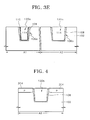
- the second STI structure 120b is formed only between PMOS transistors in the core and peripheral regions.
- the first STI structure 120a (having the relief liner 110 included) is formed in the cell region as well as in a region for providing isolation in areas that are not between PMOS transistors in the core and peripheral regions.
- the manufacturing method is substantially the same as that disclosed above in reference to FIGs. 3A to 4, except that the photoresist pattern 112 for removing the relief liner 110 is formed to define trenches only between adjacent PMOS transistors.
- the other steps may be the same as those disclosed above.
- reference numeral A3 denotes a region where circuits other than PMOS transistors are formed in the cell region, the core region and the peripheral region.
- Reference numeral A4 denotes a region having PMOS transistors formed therein.
- the pad oxide layer 102 and the silicon nitride layer 104 are formed on the semiconductor substrate 100.
- An anti-reflection film 250 is formed on the silicon nitride layer 104 to reduce reflection from the silicon nitride layer 104 during a subsequent photolithography process.
- the anti-reflection film 250 is a silicon oxynitride (SiON) layer formed to a thickness in a range between about 600 and 700 ⁇ ngstroms.
- the anti-reflection film 250, the silicon nitride layer 104, and the pad oxide layer 102 are etched using a known photolithography process to expose a pre-isolation region of the semiconductor substrate 100.
- the semiconductor substrate 100 is etched to a depth in a range between about 0.1 to 1.5 ⁇ m using the silicon nitride layer 104 as a mask, to thereby form the first and second trenches 106a and 106b.
- the first trench 106a is. formed in the cell region A1 or in the region A3 except for those portions within A3 that provide isolation between PMOS transistors.
- the second trench 106b is formed in the core and peripheral regions A2 or the region A4 for providing isolation between adjacent PMOS transistors in the core and the peripheral regions. Forming the anti-reflection film 250 on the silicon nitride layer 104 may prevent a notching phenomenon in the photolithography process.
- the STI structures that provide isolation between the core and peripheral regions or between PMOS transistors in the core and peripheral regions are formed free of the relief liner.
- the amount of negative charges trapped or remaining at the inner boundary of the STI structure can be reduced which may reduce the amount of positive charges induced at the outer boundary of the STI layer.
- a current path may not be created between the adjacent p-type doped regions of adjacent PMOS transistors and the threshold and breakdown voltages associated with the PMOS transistor can be protected.
- STI structures formed in the cell region and between adjacent n-type doped regions include the relief layer.
Landscapes
- Engineering & Computer Science (AREA)
- Physics & Mathematics (AREA)
- Condensed Matter Physics & Semiconductors (AREA)
- General Physics & Mathematics (AREA)
- Manufacturing & Machinery (AREA)
- Computer Hardware Design (AREA)
- Microelectronics & Electronic Packaging (AREA)
- Power Engineering (AREA)
- Element Separation (AREA)
- Metal-Oxide And Bipolar Metal-Oxide Semiconductor Integrated Circuits (AREA)
- Semiconductor Memories (AREA)
Priority Applications (1)
| Application Number | Priority Date | Filing Date | Title |
|---|---|---|---|
| EP04020046A EP1487011B1 (de) | 2000-12-09 | 2001-12-04 | Integrierte Schaltkreise und benachbarte Gebiete mit flachen Grabenisolations-Strukturen ohne "Liner"-Schichten dazwischen und zugehörige Herstellungsverfahren |
Applications Claiming Priority (2)
| Application Number | Priority Date | Filing Date | Title |
|---|---|---|---|
| KR10-2000-0074915A KR100382728B1 (ko) | 2000-12-09 | 2000-12-09 | 얕은 트렌치 아이솔레이션 구조를 갖는 반도체 디바이스및 그 제조방법 |
| KR2000074915 | 2000-12-09 |
Related Child Applications (1)
| Application Number | Title | Priority Date | Filing Date |
|---|---|---|---|
| EP04020046A Division EP1487011B1 (de) | 2000-12-09 | 2001-12-04 | Integrierte Schaltkreise und benachbarte Gebiete mit flachen Grabenisolations-Strukturen ohne "Liner"-Schichten dazwischen und zugehörige Herstellungsverfahren |
Publications (3)
| Publication Number | Publication Date |
|---|---|
| EP1213757A2 true EP1213757A2 (de) | 2002-06-12 |
| EP1213757A3 EP1213757A3 (de) | 2003-09-03 |
| EP1213757B1 EP1213757B1 (de) | 2007-04-11 |
Family
ID=19702879
Family Applications (2)
| Application Number | Title | Priority Date | Filing Date |
|---|---|---|---|
| EP04020046A Expired - Lifetime EP1487011B1 (de) | 2000-12-09 | 2001-12-04 | Integrierte Schaltkreise und benachbarte Gebiete mit flachen Grabenisolations-Strukturen ohne "Liner"-Schichten dazwischen und zugehörige Herstellungsverfahren |
| EP01128854A Expired - Lifetime EP1213757B1 (de) | 2000-12-09 | 2001-12-04 | Integrierte Schaltkreise und benachbarte p-dotierte Gebiete mit flachen Grabenisolations-Strukturen ohne "Liner"-Schichten dazwischen und zugehöriges Herstellungsverfahren |
Family Applications Before (1)
| Application Number | Title | Priority Date | Filing Date |
|---|---|---|---|
| EP04020046A Expired - Lifetime EP1487011B1 (de) | 2000-12-09 | 2001-12-04 | Integrierte Schaltkreise und benachbarte Gebiete mit flachen Grabenisolations-Strukturen ohne "Liner"-Schichten dazwischen und zugehörige Herstellungsverfahren |
Country Status (7)
| Country | Link |
|---|---|
| US (2) | US6642125B2 (de) |
| EP (2) | EP1487011B1 (de) |
| JP (1) | JP2002231805A (de) |
| KR (1) | KR100382728B1 (de) |
| CN (1) | CN1277300C (de) |
| DE (2) | DE60141256D1 (de) |
| TW (1) | TWI247377B (de) |
Cited By (3)
| Publication number | Priority date | Publication date | Assignee | Title |
|---|---|---|---|---|
| WO2003046991A1 (fr) * | 2001-11-26 | 2003-06-05 | Hitachi, Ltd. | Composant a semi-conducteur et procede de fabrication |
| US7479688B2 (en) * | 2003-05-30 | 2009-01-20 | International Business Machines Corporation | STI stress modification by nitrogen plasma treatment for improving performance in small width devices |
| US9331144B2 (en) | 2012-09-04 | 2016-05-03 | Ps4 Luxco S.A.R.L. | Semiconductor device and method for producing the same |
Families Citing this family (39)
| Publication number | Priority date | Publication date | Assignee | Title |
|---|---|---|---|---|
| US6906793B2 (en) * | 2000-12-11 | 2005-06-14 | Canesta, Inc. | Methods and devices for charge management for three-dimensional sensing |
| KR100413830B1 (ko) * | 2001-04-30 | 2003-12-31 | 삼성전자주식회사 | 트렌치 소자분리 구조를 가지는 반도체 소자 및 그 제조방법 |
| KR100400254B1 (ko) * | 2001-12-18 | 2003-10-01 | 주식회사 하이닉스반도체 | 반도체 소자의 제조방법 |
| JP2003273206A (ja) * | 2002-03-18 | 2003-09-26 | Fujitsu Ltd | 半導体装置とその製造方法 |
| JP2004047599A (ja) * | 2002-07-10 | 2004-02-12 | Renesas Technology Corp | 半導体装置およびその製造方法 |
| KR100443126B1 (ko) * | 2002-08-19 | 2004-08-04 | 삼성전자주식회사 | 트렌치 구조물 및 이의 형성 방법 |
| US7081395B2 (en) * | 2003-05-23 | 2006-07-25 | Taiwan Semiconductor Manufacturing Co., Ltd. | Silicon strain engineering accomplished via use of specific shallow trench isolation fill materials |
| KR100839528B1 (ko) * | 2003-06-30 | 2008-06-19 | 주식회사 하이닉스반도체 | 트렌치형 소자분리막을 갖는 반도체 소자 및 그 제조 방법 |
| KR100971432B1 (ko) * | 2003-06-30 | 2010-07-21 | 주식회사 하이닉스반도체 | 반도체 소자의 소자분리막 형성방법 |
| US7244680B2 (en) * | 2003-11-14 | 2007-07-17 | Macronix International Co., Ltd. | Method of simultaneously fabricating isolation structures having rounded and unrounded corners |
| KR100602085B1 (ko) * | 2003-12-31 | 2006-07-14 | 동부일렉트로닉스 주식회사 | 반도체 소자 및 그의 제조 방법 |
| US20050158897A1 (en) * | 2004-01-21 | 2005-07-21 | Jhy-Jyi Sze | Image sensor device and method of fabricating the same |
| KR100546161B1 (ko) * | 2004-07-13 | 2006-01-24 | 주식회사 하이닉스반도체 | 반도체 소자의 소자 분리막 제조 방법 |
| JP2006286788A (ja) * | 2005-03-31 | 2006-10-19 | Fujitsu Ltd | 半導体装置とその製造方法 |
| JP4515951B2 (ja) * | 2005-03-31 | 2010-08-04 | 富士通セミコンダクター株式会社 | 半導体装置及びその製造方法 |
| KR100695868B1 (ko) * | 2005-06-23 | 2007-03-19 | 삼성전자주식회사 | 소자 분리막과 그 제조 방법, 이를 갖는 반도체 장치 및 그제조 방법 |
| US7396728B2 (en) * | 2005-06-29 | 2008-07-08 | Texas Instruments Incorporated | Methods of improving drive currents by employing strain inducing STI liners |
| US7384861B2 (en) * | 2005-07-18 | 2008-06-10 | Texas Instruments Incorporated | Strain modulation employing process techniques for CMOS technologies |
| US7514309B2 (en) * | 2005-07-19 | 2009-04-07 | Texas Instruments Incorporated | Methods to selectively protect NMOS regions, PMOS regions, and gate layers during EPI process |
| US20070200196A1 (en) * | 2006-02-24 | 2007-08-30 | Lattice Semiconductor Corporation | Shallow trench isolation (STI) devices and processes |
| US7691722B2 (en) | 2006-03-14 | 2010-04-06 | Micron Technology, Inc. | Isolation trench fill using oxide liner and nitride etch back technique with dual trench depth capability |
| US20070267715A1 (en) * | 2006-05-18 | 2007-11-22 | Sunil Mehta | Shallow trench isolation (STI) with trench liner of increased thickness |
| US7892931B2 (en) * | 2006-12-20 | 2011-02-22 | Texas Instruments Incorporated | Use of a single mask during the formation of a transistor's drain extension and recessed strained epi regions |
| US20080205023A1 (en) * | 2007-02-27 | 2008-08-28 | International Business Machines Corporation | Electronic components on trenched substrates and method of forming same |
| KR100891534B1 (ko) * | 2007-10-26 | 2009-04-03 | 주식회사 하이닉스반도체 | 반도체 소자의 제조방법 |
| US20090191688A1 (en) * | 2008-01-28 | 2009-07-30 | Texas Instruments Incorporated | Shallow Trench Isolation Process Using Two Liners |
| KR101446331B1 (ko) * | 2008-02-13 | 2014-10-02 | 삼성전자주식회사 | 반도체 소자의 제조 방법 |
| US8003482B2 (en) | 2009-11-19 | 2011-08-23 | Micron Technology, Inc. | Methods of processing semiconductor substrates in forming scribe line alignment marks |
| CN102693932B (zh) * | 2011-03-23 | 2014-06-11 | 中芯国际集成电路制造(上海)有限公司 | 浅沟槽隔离结构的制造方法 |
| DK177321B1 (en) * | 2011-05-10 | 2013-01-02 | Skandinavisk HTP ApS | Paper for transfer pattern printing |
| CN102412184B (zh) * | 2011-05-23 | 2014-03-12 | 上海华力微电子有限公司 | 离子注入调整隔离氧化物应力的浅沟槽隔离结构制备方法 |
| US8927387B2 (en) * | 2012-04-09 | 2015-01-06 | International Business Machines Corporation | Robust isolation for thin-box ETSOI MOSFETS |
| US9006080B2 (en) * | 2013-03-12 | 2015-04-14 | Taiwan Semiconductor Manufacturing Company, Ltd. | Varied STI liners for isolation structures in image sensing devices |
| CN104240762B (zh) * | 2013-06-09 | 2018-06-01 | 中芯国际集成电路制造(上海)有限公司 | 反熔丝结构及编程方法 |
| CN105826191B (zh) * | 2015-01-07 | 2019-09-17 | 中芯国际集成电路制造(上海)有限公司 | 浅沟槽隔离结构的制备方法 |
| CN106711213B (zh) * | 2015-07-20 | 2021-02-26 | 联华电子股份有限公司 | 半导体元件及其制作方法 |
| US9812548B2 (en) * | 2015-09-08 | 2017-11-07 | Maxpower Semiconductor, Inc. | Power device having a polysilicon-filled trench with a tapered oxide thickness |
| US11335770B2 (en) | 2020-05-28 | 2022-05-17 | Winbond Electronics Corp. | Semiconductor isolation structures having different configurations in different device regions and method of forming the same |
| CN116344623B (zh) * | 2023-05-30 | 2023-08-22 | 粤芯半导体技术股份有限公司 | 高压mos器件及其制备方法 |
Citations (9)
| Publication number | Priority date | Publication date | Assignee | Title |
|---|---|---|---|---|
| JPH07176606A (ja) * | 1993-12-21 | 1995-07-14 | Toshiba Corp | 半導体装置およびその製造方法 |
| JPH11220017A (ja) * | 1998-01-30 | 1999-08-10 | Mitsubishi Electric Corp | 半導体装置とその製造方法 |
| US5940717A (en) * | 1997-12-30 | 1999-08-17 | Siemens Aktiengesellschaft | Recessed shallow trench isolation structure nitride liner and method for making same |
| JPH11284137A (ja) * | 1998-03-30 | 1999-10-15 | Nippon Steel Corp | 半導体記憶装置及びその製造方法 |
| US5990002A (en) * | 1997-04-18 | 1999-11-23 | Micron Technology, Inc | Method of making an antireflective structure |
| EP0967636A2 (de) * | 1998-06-16 | 1999-12-29 | Siemens Aktiengesellschaft | Elektrisch isolierte Halbleiter-Anordnungen |
| JP2000124303A (ja) * | 1998-10-09 | 2000-04-28 | Samsung Electronics Co Ltd | トレンチ隔離の製造方法 |
| US6064105A (en) * | 1997-10-09 | 2000-05-16 | Vantis Corporation | Data retention of EEPROM cell with shallow trench isolation using thicker liner oxide |
| US6143635A (en) * | 1998-02-19 | 2000-11-07 | International Business Machines Corporation | Field effect transistors with improved implants and method for making such transistors |
Family Cites Families (5)
| Publication number | Priority date | Publication date | Assignee | Title |
|---|---|---|---|---|
| JPS5848936A (ja) * | 1981-09-10 | 1983-03-23 | Fujitsu Ltd | 半導体装置の製造方法 |
| JPH02273956A (ja) * | 1989-04-15 | 1990-11-08 | Fujitsu Ltd | 半導体装置及びその製造方法 |
| US5981341A (en) * | 1997-12-05 | 1999-11-09 | Advanced Micro Devices | Sidewall spacer for protecting tunnel oxide during isolation trench formation in self-aligned flash memory core |
| KR20000009808A (ko) * | 1998-07-28 | 2000-02-15 | 윤종용 | 트렌치 격리의 제조 방법 |
| US6468849B1 (en) * | 1999-06-11 | 2002-10-22 | Texas Instruments Incorporated | Methods and devices for optimized digital and analog CMOS transistor performance in deep submicron technology |
-
2000
- 2000-12-09 KR KR10-2000-0074915A patent/KR100382728B1/ko active IP Right Grant
-
2001
- 2001-11-30 TW TW090129618A patent/TWI247377B/zh not_active IP Right Cessation
- 2001-12-04 EP EP04020046A patent/EP1487011B1/de not_active Expired - Lifetime
- 2001-12-04 EP EP01128854A patent/EP1213757B1/de not_active Expired - Lifetime
- 2001-12-04 DE DE60141256T patent/DE60141256D1/de not_active Expired - Lifetime
- 2001-12-04 DE DE60127799T patent/DE60127799T2/de not_active Expired - Lifetime
- 2001-12-07 CN CNB011396989A patent/CN1277300C/zh not_active Expired - Lifetime
- 2001-12-07 US US10/021,165 patent/US6642125B2/en not_active Expired - Lifetime
- 2001-12-07 JP JP2001374719A patent/JP2002231805A/ja not_active Ceased
-
2003
- 2003-07-31 US US10/631,602 patent/US20040021197A1/en not_active Abandoned
Patent Citations (9)
| Publication number | Priority date | Publication date | Assignee | Title |
|---|---|---|---|---|
| JPH07176606A (ja) * | 1993-12-21 | 1995-07-14 | Toshiba Corp | 半導体装置およびその製造方法 |
| US5990002A (en) * | 1997-04-18 | 1999-11-23 | Micron Technology, Inc | Method of making an antireflective structure |
| US6064105A (en) * | 1997-10-09 | 2000-05-16 | Vantis Corporation | Data retention of EEPROM cell with shallow trench isolation using thicker liner oxide |
| US5940717A (en) * | 1997-12-30 | 1999-08-17 | Siemens Aktiengesellschaft | Recessed shallow trench isolation structure nitride liner and method for making same |
| JPH11220017A (ja) * | 1998-01-30 | 1999-08-10 | Mitsubishi Electric Corp | 半導体装置とその製造方法 |
| US6143635A (en) * | 1998-02-19 | 2000-11-07 | International Business Machines Corporation | Field effect transistors with improved implants and method for making such transistors |
| JPH11284137A (ja) * | 1998-03-30 | 1999-10-15 | Nippon Steel Corp | 半導体記憶装置及びその製造方法 |
| EP0967636A2 (de) * | 1998-06-16 | 1999-12-29 | Siemens Aktiengesellschaft | Elektrisch isolierte Halbleiter-Anordnungen |
| JP2000124303A (ja) * | 1998-10-09 | 2000-04-28 | Samsung Electronics Co Ltd | トレンチ隔離の製造方法 |
Non-Patent Citations (4)
| Title |
|---|
| PATENT ABSTRACTS OF JAPAN vol. 1995, no. 10, 30 November 1995 (1995-11-30) & JP 07 176606 A (TOSHIBA CORP), 14 July 1995 (1995-07-14) * |
| PATENT ABSTRACTS OF JAPAN vol. 1999, no. 13, 30 November 1999 (1999-11-30) & JP 11 220017 A (MITSUBISHI ELECTRIC CORP), 10 August 1999 (1999-08-10) & US 6 245 641 B1 (SHIOZAWA KATSUOMI ET AL) 12 June 2001 (2001-06-12) * |
| PATENT ABSTRACTS OF JAPAN vol. 2000, no. 01, 31 January 2000 (2000-01-31) & JP 11 284137 A (NIPPON STEEL CORP), 15 October 1999 (1999-10-15) * |
| PATENT ABSTRACTS OF JAPAN vol. 2000, no. 07, 29 September 2000 (2000-09-29) & JP 2000 124303 A (SAMSUNG ELECTRONICS CO LTD), 28 April 2000 (2000-04-28) & US 6 251 746 B1 (KOO BON-YOUNG ET AL) 26 June 2001 (2001-06-26) * |
Cited By (4)
| Publication number | Priority date | Publication date | Assignee | Title |
|---|---|---|---|---|
| WO2003046991A1 (fr) * | 2001-11-26 | 2003-06-05 | Hitachi, Ltd. | Composant a semi-conducteur et procede de fabrication |
| US7244643B2 (en) | 2001-11-26 | 2007-07-17 | Hitachi, Ltd. | Semiconductor device and manufacturing method thereof |
| US7479688B2 (en) * | 2003-05-30 | 2009-01-20 | International Business Machines Corporation | STI stress modification by nitrogen plasma treatment for improving performance in small width devices |
| US9331144B2 (en) | 2012-09-04 | 2016-05-03 | Ps4 Luxco S.A.R.L. | Semiconductor device and method for producing the same |
Also Published As
| Publication number | Publication date |
|---|---|
| DE60127799T2 (de) | 2007-12-27 |
| DE60141256D1 (de) | 2010-03-25 |
| EP1487011A1 (de) | 2004-12-15 |
| KR100382728B1 (ko) | 2003-05-09 |
| US20040021197A1 (en) | 2004-02-05 |
| KR20020045656A (ko) | 2002-06-20 |
| CN1359145A (zh) | 2002-07-17 |
| JP2002231805A (ja) | 2002-08-16 |
| EP1213757A3 (de) | 2003-09-03 |
| EP1487011B1 (de) | 2010-02-03 |
| EP1213757B1 (de) | 2007-04-11 |
| TWI247377B (en) | 2006-01-11 |
| US6642125B2 (en) | 2003-11-04 |
| DE60127799D1 (de) | 2007-05-24 |
| US20020070420A1 (en) | 2002-06-13 |
| CN1277300C (zh) | 2006-09-27 |
Similar Documents
| Publication | Publication Date | Title |
|---|---|---|
| US6642125B2 (en) | Integrated circuits having adjacent P-type doped regions having shallow trench isolation structures without liner layers therein therebetween and methods of forming same | |
| US6670689B2 (en) | Semiconductor device having shallow trench isolation structure | |
| US6486517B2 (en) | Semiconductor device having shallow trench isolation structure and manufacturing method thereof | |
| US6482715B2 (en) | Method of forming shallow trench isolation layer in semiconductor device | |
| US6326282B1 (en) | Method of forming trench isolation in a semiconductor device and structure formed thereby | |
| US6069057A (en) | Method for fabricating trench-isolation structure | |
| US6586804B2 (en) | Shallow trench isolation type semiconductor device and method of manufacturing the same | |
| US8384188B2 (en) | Semiconductor device and fabrication method thereof | |
| US20020127818A1 (en) | Recess-free trench isolation structure and method of forming the same | |
| US6913978B1 (en) | Method for forming shallow trench isolation structure | |
| KR100271399B1 (ko) | 반도체 소자 분리를 위한 얕은 트랜치 제조 방법 | |
| US6344374B1 (en) | Method of fabricating insulators for isolating electronic devices | |
| JP4592193B2 (ja) | 半導体装置の製造方法 | |
| JP2004296754A (ja) | 半導体装置および半導体装置の製造方法 | |
| KR101025731B1 (ko) | 라이너질화막을 포함하는 반도체소자의 소자분리막 및 그제조 방법 | |
| KR100289663B1 (ko) | 반도체 소자의 소자 분리막 형성방법 | |
| US20020068415A1 (en) | Method of fabricating a shallow trench isolation structure | |
| KR101022672B1 (ko) | 트렌치형 소자분리를 갖는 반도체소자 및 그의 제조 방법 | |
| JP2006222418A (ja) | 半導体装置の製造方法 | |
| KR20030055997A (ko) | 얕은 트렌치 아이솔레이션 구조를 갖는 반도체 장치 및 그형성방법 | |
| KR20050010251A (ko) | 반도체소자의 소자분리막 형성방법 |
Legal Events
| Date | Code | Title | Description |
|---|---|---|---|
| PUAI | Public reference made under article 153(3) epc to a published international application that has entered the european phase |
Free format text: ORIGINAL CODE: 0009012 |
|
| 17P | Request for examination filed |
Effective date: 20011204 |
|
| AK | Designated contracting states |
Kind code of ref document: A2 Designated state(s): AT BE CH CY DE DK ES FI FR GB GR IE IT LI LU MC NL PT SE TR |
|
| AX | Request for extension of the european patent |
Free format text: AL;LT;LV;MK;RO;SI |
|
| PUAL | Search report despatched |
Free format text: ORIGINAL CODE: 0009013 |
|
| AK | Designated contracting states |
Kind code of ref document: A3 Designated state(s): AT BE CH CY DE DK ES FI FR GB GR IE IT LI LU MC NL PT SE TR |
|
| AX | Request for extension of the european patent |
Extension state: AL LT LV MK RO SI |
|
| 17Q | First examination report despatched |
Effective date: 20040212 |
|
| AKX | Designation fees paid |
Designated state(s): DE FR GB |
|
| 17Q | First examination report despatched |
Effective date: 20040212 |
|
| GRAP | Despatch of communication of intention to grant a patent |
Free format text: ORIGINAL CODE: EPIDOSNIGR1 |
|
| RTI1 | Title (correction) |
Free format text: INTEGRATED CIRCUITS HAVING ADJACENT P-TYPE DOPED REGIONS HAVING SHALLOW TRENCH ISOLATION STRUCTURES WITHOUT LINER LAYERS THEREBETWEEN AND METHODS OF FORMING SAME |
|
| GRAS | Grant fee paid |
Free format text: ORIGINAL CODE: EPIDOSNIGR3 |
|
| GRAA | (expected) grant |
Free format text: ORIGINAL CODE: 0009210 |
|
| AK | Designated contracting states |
Kind code of ref document: B1 Designated state(s): DE FR GB |
|
| REG | Reference to a national code |
Ref country code: GB Ref legal event code: FG4D |
|
| REF | Corresponds to: |
Ref document number: 60127799 Country of ref document: DE Date of ref document: 20070524 Kind code of ref document: P |
|
| ET | Fr: translation filed | ||
| PLBE | No opposition filed within time limit |
Free format text: ORIGINAL CODE: 0009261 |
|
| STAA | Information on the status of an ep patent application or granted ep patent |
Free format text: STATUS: NO OPPOSITION FILED WITHIN TIME LIMIT |
|
| 26N | No opposition filed |
Effective date: 20080114 |
|
| REG | Reference to a national code |
Ref country code: FR Ref legal event code: PLFP Year of fee payment: 15 |
|
| REG | Reference to a national code |
Ref country code: FR Ref legal event code: PLFP Year of fee payment: 16 |
|
| REG | Reference to a national code |
Ref country code: FR Ref legal event code: PLFP Year of fee payment: 17 |
|
| PGFP | Annual fee paid to national office [announced via postgrant information from national office to epo] |
Ref country code: DE Payment date: 20201119 Year of fee payment: 20 Ref country code: FR Payment date: 20201120 Year of fee payment: 20 Ref country code: GB Payment date: 20201123 Year of fee payment: 20 |
|
| REG | Reference to a national code |
Ref country code: DE Ref legal event code: R071 Ref document number: 60127799 Country of ref document: DE |
|
| REG | Reference to a national code |
Ref country code: GB Ref legal event code: PE20 Expiry date: 20211203 |
|
| PG25 | Lapsed in a contracting state [announced via postgrant information from national office to epo] |
Ref country code: GB Free format text: LAPSE BECAUSE OF EXPIRATION OF PROTECTION Effective date: 20211203 |