EP0978729A2 - Hochfrequenz-Sende-Empfangsvorrichtung für Fahrzeug-Radarsysteme - Google Patents
Hochfrequenz-Sende-Empfangsvorrichtung für Fahrzeug-Radarsysteme Download PDFInfo
- Publication number
- EP0978729A2 EP0978729A2 EP99306230A EP99306230A EP0978729A2 EP 0978729 A2 EP0978729 A2 EP 0978729A2 EP 99306230 A EP99306230 A EP 99306230A EP 99306230 A EP99306230 A EP 99306230A EP 0978729 A2 EP0978729 A2 EP 0978729A2
- Authority
- EP
- European Patent Office
- Prior art keywords
- circuit
- antenna
- base plate
- frequency
- transceiver circuit
- Prior art date
- Legal status (The legal status is an assumption and is not a legal conclusion. Google has not performed a legal analysis and makes no representation as to the accuracy of the status listed.)
- Withdrawn
Links
Images


Classifications
-
- H—ELECTRICITY
- H01—ELECTRIC ELEMENTS
- H01L—SEMICONDUCTOR DEVICES NOT COVERED BY CLASS H10
- H01L23/00—Details of semiconductor or other solid state devices
- H01L23/58—Structural electrical arrangements for semiconductor devices not otherwise provided for, e.g. in combination with batteries
- H01L23/64—Impedance arrangements
- H01L23/66—High-frequency adaptations
-
- G—PHYSICS
- G01—MEASURING; TESTING
- G01S—RADIO DIRECTION-FINDING; RADIO NAVIGATION; DETERMINING DISTANCE OR VELOCITY BY USE OF RADIO WAVES; LOCATING OR PRESENCE-DETECTING BY USE OF THE REFLECTION OR RERADIATION OF RADIO WAVES; ANALOGOUS ARRANGEMENTS USING OTHER WAVES
- G01S7/00—Details of systems according to groups G01S13/00, G01S15/00, G01S17/00
- G01S7/02—Details of systems according to groups G01S13/00, G01S15/00, G01S17/00 of systems according to group G01S13/00
- G01S7/03—Details of HF subsystems specially adapted therefor, e.g. common to transmitter and receiver
- G01S7/032—Constructional details for solid-state radar subsystems
-
- H—ELECTRICITY
- H01—ELECTRIC ELEMENTS
- H01Q—ANTENNAS, i.e. RADIO AERIALS
- H01Q1/00—Details of, or arrangements associated with, antennas
- H01Q1/27—Adaptation for use in or on movable bodies
- H01Q1/32—Adaptation for use in or on road or rail vehicles
- H01Q1/3208—Adaptation for use in or on road or rail vehicles characterised by the application wherein the antenna is used
- H01Q1/3233—Adaptation for use in or on road or rail vehicles characterised by the application wherein the antenna is used particular used as part of a sensor or in a security system, e.g. for automotive radar, navigation systems
-
- H—ELECTRICITY
- H01—ELECTRIC ELEMENTS
- H01Q—ANTENNAS, i.e. RADIO AERIALS
- H01Q21/00—Antenna arrays or systems
- H01Q21/0087—Apparatus or processes specially adapted for manufacturing antenna arrays
-
- H—ELECTRICITY
- H01—ELECTRIC ELEMENTS
- H01Q—ANTENNAS, i.e. RADIO AERIALS
- H01Q23/00—Antennas with active circuits or circuit elements integrated within them or attached to them
-
- G—PHYSICS
- G01—MEASURING; TESTING
- G01S—RADIO DIRECTION-FINDING; RADIO NAVIGATION; DETERMINING DISTANCE OR VELOCITY BY USE OF RADIO WAVES; LOCATING OR PRESENCE-DETECTING BY USE OF THE REFLECTION OR RERADIATION OF RADIO WAVES; ANALOGOUS ARRANGEMENTS USING OTHER WAVES
- G01S13/00—Systems using the reflection or reradiation of radio waves, e.g. radar systems; Analogous systems using reflection or reradiation of waves whose nature or wavelength is irrelevant or unspecified
- G01S13/88—Radar or analogous systems specially adapted for specific applications
- G01S13/93—Radar or analogous systems specially adapted for specific applications for anti-collision purposes
- G01S13/931—Radar or analogous systems specially adapted for specific applications for anti-collision purposes of land vehicles
- G01S2013/9325—Radar or analogous systems specially adapted for specific applications for anti-collision purposes of land vehicles for inter-vehicle distance regulation, e.g. navigating in platoons
-
- G—PHYSICS
- G01—MEASURING; TESTING
- G01S—RADIO DIRECTION-FINDING; RADIO NAVIGATION; DETERMINING DISTANCE OR VELOCITY BY USE OF RADIO WAVES; LOCATING OR PRESENCE-DETECTING BY USE OF THE REFLECTION OR RERADIATION OF RADIO WAVES; ANALOGOUS ARRANGEMENTS USING OTHER WAVES
- G01S7/00—Details of systems according to groups G01S13/00, G01S15/00, G01S17/00
- G01S7/02—Details of systems according to groups G01S13/00, G01S15/00, G01S17/00 of systems according to group G01S13/00
- G01S7/03—Details of HF subsystems specially adapted therefor, e.g. common to transmitter and receiver
-
- H—ELECTRICITY
- H01—ELECTRIC ELEMENTS
- H01L—SEMICONDUCTOR DEVICES NOT COVERED BY CLASS H10
- H01L2223/00—Details relating to semiconductor or other solid state devices covered by the group H01L23/00
- H01L2223/58—Structural electrical arrangements for semiconductor devices not otherwise provided for
- H01L2223/64—Impedance arrangements
- H01L2223/66—High-frequency adaptations
- H01L2223/6605—High-frequency electrical connections
- H01L2223/6627—Waveguides, e.g. microstrip line, strip line, coplanar line
-
- H—ELECTRICITY
- H01—ELECTRIC ELEMENTS
- H01L—SEMICONDUCTOR DEVICES NOT COVERED BY CLASS H10
- H01L2223/00—Details relating to semiconductor or other solid state devices covered by the group H01L23/00
- H01L2223/58—Structural electrical arrangements for semiconductor devices not otherwise provided for
- H01L2223/64—Impedance arrangements
- H01L2223/66—High-frequency adaptations
- H01L2223/6661—High-frequency adaptations for passive devices
- H01L2223/6677—High-frequency adaptations for passive devices for antenna, e.g. antenna included within housing of semiconductor device
-
- H—ELECTRICITY
- H01—ELECTRIC ELEMENTS
- H01L—SEMICONDUCTOR DEVICES NOT COVERED BY CLASS H10
- H01L2224/00—Indexing scheme for arrangements for connecting or disconnecting semiconductor or solid-state bodies and methods related thereto as covered by H01L24/00
- H01L2224/01—Means for bonding being attached to, or being formed on, the surface to be connected, e.g. chip-to-package, die-attach, "first-level" interconnects; Manufacturing methods related thereto
- H01L2224/02—Bonding areas; Manufacturing methods related thereto
- H01L2224/04—Structure, shape, material or disposition of the bonding areas prior to the connecting process
- H01L2224/05—Structure, shape, material or disposition of the bonding areas prior to the connecting process of an individual bonding area
- H01L2224/0554—External layer
- H01L2224/05599—Material
-
- H—ELECTRICITY
- H01—ELECTRIC ELEMENTS
- H01L—SEMICONDUCTOR DEVICES NOT COVERED BY CLASS H10
- H01L2224/00—Indexing scheme for arrangements for connecting or disconnecting semiconductor or solid-state bodies and methods related thereto as covered by H01L24/00
- H01L2224/01—Means for bonding being attached to, or being formed on, the surface to be connected, e.g. chip-to-package, die-attach, "first-level" interconnects; Manufacturing methods related thereto
- H01L2224/42—Wire connectors; Manufacturing methods related thereto
- H01L2224/47—Structure, shape, material or disposition of the wire connectors after the connecting process
- H01L2224/48—Structure, shape, material or disposition of the wire connectors after the connecting process of an individual wire connector
- H01L2224/4805—Shape
- H01L2224/4809—Loop shape
- H01L2224/48091—Arched
-
- H—ELECTRICITY
- H01—ELECTRIC ELEMENTS
- H01L—SEMICONDUCTOR DEVICES NOT COVERED BY CLASS H10
- H01L2224/00—Indexing scheme for arrangements for connecting or disconnecting semiconductor or solid-state bodies and methods related thereto as covered by H01L24/00
- H01L2224/80—Methods for connecting semiconductor or other solid state bodies using means for bonding being attached to, or being formed on, the surface to be connected
- H01L2224/85—Methods for connecting semiconductor or other solid state bodies using means for bonding being attached to, or being formed on, the surface to be connected using a wire connector
- H01L2224/8538—Bonding interfaces outside the semiconductor or solid-state body
- H01L2224/85399—Material
-
- H—ELECTRICITY
- H01—ELECTRIC ELEMENTS
- H01L—SEMICONDUCTOR DEVICES NOT COVERED BY CLASS H10
- H01L24/00—Arrangements for connecting or disconnecting semiconductor or solid-state bodies; Methods or apparatus related thereto
- H01L24/01—Means for bonding being attached to, or being formed on, the surface to be connected, e.g. chip-to-package, die-attach, "first-level" interconnects; Manufacturing methods related thereto
- H01L24/42—Wire connectors; Manufacturing methods related thereto
- H01L24/47—Structure, shape, material or disposition of the wire connectors after the connecting process
- H01L24/48—Structure, shape, material or disposition of the wire connectors after the connecting process of an individual wire connector
-
- H—ELECTRICITY
- H01—ELECTRIC ELEMENTS
- H01L—SEMICONDUCTOR DEVICES NOT COVERED BY CLASS H10
- H01L2924/00—Indexing scheme for arrangements or methods for connecting or disconnecting semiconductor or solid-state bodies as covered by H01L24/00
- H01L2924/0001—Technical content checked by a classifier
- H01L2924/00014—Technical content checked by a classifier the subject-matter covered by the group, the symbol of which is combined with the symbol of this group, being disclosed without further technical details
-
- H—ELECTRICITY
- H01—ELECTRIC ELEMENTS
- H01L—SEMICONDUCTOR DEVICES NOT COVERED BY CLASS H10
- H01L2924/00—Indexing scheme for arrangements or methods for connecting or disconnecting semiconductor or solid-state bodies as covered by H01L24/00
- H01L2924/01—Chemical elements
- H01L2924/0102—Calcium [Ca]
-
- H—ELECTRICITY
- H01—ELECTRIC ELEMENTS
- H01L—SEMICONDUCTOR DEVICES NOT COVERED BY CLASS H10
- H01L2924/00—Indexing scheme for arrangements or methods for connecting or disconnecting semiconductor or solid-state bodies as covered by H01L24/00
- H01L2924/01—Chemical elements
- H01L2924/01078—Platinum [Pt]
-
- H—ELECTRICITY
- H01—ELECTRIC ELEMENTS
- H01L—SEMICONDUCTOR DEVICES NOT COVERED BY CLASS H10
- H01L2924/00—Indexing scheme for arrangements or methods for connecting or disconnecting semiconductor or solid-state bodies as covered by H01L24/00
- H01L2924/095—Indexing scheme for arrangements or methods for connecting or disconnecting semiconductor or solid-state bodies as covered by H01L24/00 with a principal constituent of the material being a combination of two or more materials provided in the groups H01L2924/013 - H01L2924/0715
- H01L2924/097—Glass-ceramics, e.g. devitrified glass
- H01L2924/09701—Low temperature co-fired ceramic [LTCC]
-
- H—ELECTRICITY
- H01—ELECTRIC ELEMENTS
- H01L—SEMICONDUCTOR DEVICES NOT COVERED BY CLASS H10
- H01L2924/00—Indexing scheme for arrangements or methods for connecting or disconnecting semiconductor or solid-state bodies as covered by H01L24/00
- H01L2924/10—Details of semiconductor or other solid state devices to be connected
- H01L2924/11—Device type
- H01L2924/12—Passive devices, e.g. 2 terminal devices
- H01L2924/1204—Optical Diode
- H01L2924/12042—LASER
-
- H—ELECTRICITY
- H01—ELECTRIC ELEMENTS
- H01L—SEMICONDUCTOR DEVICES NOT COVERED BY CLASS H10
- H01L2924/00—Indexing scheme for arrangements or methods for connecting or disconnecting semiconductor or solid-state bodies as covered by H01L24/00
- H01L2924/10—Details of semiconductor or other solid state devices to be connected
- H01L2924/11—Device type
- H01L2924/14—Integrated circuits
- H01L2924/141—Analog devices
- H01L2924/1423—Monolithic Microwave Integrated Circuit [MMIC]
-
- H—ELECTRICITY
- H01—ELECTRIC ELEMENTS
- H01L—SEMICONDUCTOR DEVICES NOT COVERED BY CLASS H10
- H01L2924/00—Indexing scheme for arrangements or methods for connecting or disconnecting semiconductor or solid-state bodies as covered by H01L24/00
- H01L2924/15—Details of package parts other than the semiconductor or other solid state devices to be connected
- H01L2924/151—Die mounting substrate
- H01L2924/1515—Shape
- H01L2924/15153—Shape the die mounting substrate comprising a recess for hosting the device
-
- H—ELECTRICITY
- H01—ELECTRIC ELEMENTS
- H01L—SEMICONDUCTOR DEVICES NOT COVERED BY CLASS H10
- H01L2924/00—Indexing scheme for arrangements or methods for connecting or disconnecting semiconductor or solid-state bodies as covered by H01L24/00
- H01L2924/15—Details of package parts other than the semiconductor or other solid state devices to be connected
- H01L2924/151—Die mounting substrate
- H01L2924/1517—Multilayer substrate
-
- H—ELECTRICITY
- H01—ELECTRIC ELEMENTS
- H01L—SEMICONDUCTOR DEVICES NOT COVERED BY CLASS H10
- H01L2924/00—Indexing scheme for arrangements or methods for connecting or disconnecting semiconductor or solid-state bodies as covered by H01L24/00
- H01L2924/15—Details of package parts other than the semiconductor or other solid state devices to be connected
- H01L2924/161—Cap
- H01L2924/1615—Shape
- H01L2924/16152—Cap comprising a cavity for hosting the device, e.g. U-shaped cap
-
- H—ELECTRICITY
- H01—ELECTRIC ELEMENTS
- H01L—SEMICONDUCTOR DEVICES NOT COVERED BY CLASS H10
- H01L2924/00—Indexing scheme for arrangements or methods for connecting or disconnecting semiconductor or solid-state bodies as covered by H01L24/00
- H01L2924/19—Details of hybrid assemblies other than the semiconductor or other solid state devices to be connected
- H01L2924/1901—Structure
- H01L2924/1903—Structure including wave guides
Definitions
- the present invention relates generally to a high-frequency transmitter-receiver apparatus which can be employed as a radar for an automobile or motor vehicle, a communication device in a wireless LAN (local area network) and others. Further, the present invention is concerned with an antenna unit incorporating a high-frequency transmitter-receiver device and a vehicle-onboard radar system incorporating the same.
- the high-frequency transmitter-receiver apparatus employed as the vehicle radar, the wireless LAN or the like, it is important to realize the high-frequency transmitter-receiver apparatus in a miniaturized and simplified structure from the standpoint of mountability and portability of the apparatus.
- a millimeter-wave (60 GHz band) transmitter-receiver circuit or transceiver circuit is realized as a discrete transmitter-receiver unit encased within a housing.
- an antenna unit is also realized as a discrete unit and adapted to be connected to the transceiver circuit unit. More specifically, a waveguide terminal serving as input/output terminal for the radio-frequency or RF signal is provided on a rear or bottom surface of the transmitter-receiver unit. Similarly, the antenna unit is equipped with a corresponding waveguide terminal. Thus, the transmitter-receiver unit and the antenna unit can be electrically interconnected by using a waveguide.
- JP-A-8-250913 (hereinafter referred to as the prior art reference 2), there is disclosed a high-frequency transmitter-receiver apparatus in which a planar antenna is formed on an outer surface of a package in which a monolithic microwave integrated circuit (hereinafter referred as MMIC) is hermetically accommodated.
- MMIC monolithic microwave integrated circuit
- Figure 18 of the accompanying drawings shows a structure of the same. As can be seen in the figure, an antenna 142 is mounted on a bottom surface 141 of the package while a MMIC 143 is mounted as embedded within the package in opposition to the antenna 142.
- the bottom surface of the MMIC package 143 that is, the top surface of the MMIC package 143 as viewed in the figure, is provided with a slot 146 formed by removing partially a ground conductor layer 145.
- a conductor pattern 144 constituting a part of a high-frequency circuit and provided on the bottom surface of the MMIC package 143 and the antenna 142 are coupled electromagnetically through the medium of the slot 146.
- a bonding pad 147 provided on the surface of the MMIC package 143 and a power source terminal 149 also provided on the same surface for receiving external power supply are electrically interconnected by a bonding wire 148.
- the transceiver unit and the antenna unit designed and realized discretely from each other are interconnected for constituting the high-frequency transmitter-receiver apparatus.
- This structure is certainly advantageous in that the characteristics of the transceiver unit and the antenna unit can be evaluated independent of each other.
- a large number of parts are required with the structure being complicated, which makes it difficult to realize the high-frequency transmitter-receiver apparatus in a miniaturized and simplified structure.
- coupling of the discrete units through the waveguide in a very high frequency band such as a millimeter wave band involves complexity in machining the waveguide, terminals and others, giving rise to a problem of high manufacturing cost.
- the high-frequency transceiver circuit and the antenna are electromagnetically coupled through the slot.
- insertion loss of the high-frequency signal tends to increase.
- the thickness of the electrically conductive plate 141 disposed between the antenna and the high-frequency transceiver circuit has to be reduced as thin as possible.
- the thickness of the electrically conductive plate mentioned above is on the order of 0.5 to 0.7 mm.
- the thickness of the electrically conductive plate has to be further decreased.
- the electromagnetic coupling of the signal of short wavelength such as millimeter-wave requires high dimensional precision for realizing the slot as well as high-precision positioning of the antenna pattern 142 and the high-frequency circuit pattern 144, which of course imposes not a little burden on the assembling work.
- the whole package in order to assure reliability of the MMIC, the whole package must be implemented in a hermetically sealed structure, which renders the assembling work more difficult.
- Another object of the present invention is to provide an antenna unit which incorporates as an integral part thereof a high-frequency transmitter-receiver device and in which the problems such as mentioned above are solved satisfactorily.
- a high-frequency transmitter-receiver apparatus in which a high-frequency transceiver circuit composed of an oscillator, an amplifier, a mixer circuit and the like is realized in the form of a planar circuit structure by using a dielectric substrate and a semiconductor chip, while an antenna for transmitting and receiving a high-frequency signal is realized as a planar antenna by using a dielectric substrate, wherein the dielectric substrate constituting a part of the planar circuit structure and the dielectric substrate constituting a part of the planar antenna are directly bonded on first and second surfaces, respectively, of a single electrically conductive base plate, the first and second surfaces being opposite to each other, and wherein high-frequency signal lines of the planar circuit and the planar antenna, respectively, are interconnected by an coaxial line which extends through the base plate.
- the apparatus can be miniaturized as a whole.
- those portions of the coaxial line (coaxial cable) where the coaxial line is connected, respectively, to the dielectric substrate constituting a part of the planar circuit structure and the dielectric substrate constituting a part of the planar antenna structure should preferably be realized in an airtight structure by using a dielectric such as glass, ceramic or the like.
- the transceiver circuit structure including the semiconductor chip can be realized in a hermetically sealed structure without any appreciable difficulty.
- a high-frequency transmitter-receiver apparatus which includes a base plate, an antenna provided on a first surface of the base plate, a transceiver circuit provided on a second surface of the base plate opposite to the first surface and electrically connected to the antenna, and a terminal for external connection provided on the second surface of the base plate for supplying a source current to the transceiver circuit or outputting an electric signal.
- the base plate is provided with a concave portion in the first surface and covered with the antenna and a through-hole extending through the concave portion and the second surface.
- a connecting terminal for supplying a source current to the transceiver circuit or outputting a signal extends through the through-hole and connected to the terminal for external connection in the concave portion.
- the connecting terminal is implemented in a line structure having a metal conductor electrically insulated from the base plate in the through-hole.
- the coaxial line interconnecting the high-frequency transceiver circuit and the antenna on one hand and the coaxial line for the terminal for receiving D.C. bias or power supply and/or the input/output terminal for an IF (intermediate frequency) signal on the other hand should be realized in a same structure and disposed in a same orientation. Owing to such arrangement, the work efficiency in assembling the apparatus can be enhanced, and additionally common use of the circuit components can be achieved.
- the coaxial line of a same structure can be used not only as the connecting terminal but also for interconnection of the transceiver circuit and the antenna.
- the transceiver circuit including the semiconductor chip can be realized in a hermetically sealed structure without any appreciable difficulty.
- FIG. 1 is a sectional view showing a high-frequency transmitter-receiver apparatus according to an embodiment of the present invention.
- the high-frequency transmitter-receiver apparatus includes a base plate 1 made of a metal and having a top surface on which an antenna substrate 2 formed of a dielectric for constituting an antenna is bonded and a bottom surface on which a circuit substrate 3 formed of a dielectric for constituting a transmitter-receiver or transceiver circuit and a monolithic microwave integrated circuit semiconductor chip (hereinafter referred to as the MMIC semiconductor chip or simply as the semiconductor chip) 4 are mounted by bonding.
- the MMIC semiconductor chip monolithic microwave integrated circuit semiconductor chip
- Metal patterns 10 on circuit substrate deposited on the surface of the circuit substrate 3 and metal patterns 7 on antenna substrate deposited on the surface of the antenna substrate 2 are electrically connected to each other by a center conductor 6 of a coaxial line. Since the semiconductor chip 4 is not packaged, the transceiver circuit is hermetically sealed by means of a cover 5 of transceiver components made of a metal. Mounted locally on the transceiver component cover 5 are terminals 12 for the external connection to a power source and for an IF (intermediate frequency) signal, being electrically insulated from the conductor plate (base plate) and the transceiver component cover 5, respectively, by insulation materials 8 and 9.
- IF intermediate frequency
- the terminals 12 for external connection (hereinafter referred to as the external terminal only for convenience of description) and the transceiver circuit on one hand and the circuit pattern conductor and the semiconductor chip on the other hand are interconnected by bonding wires 11.
- the semiconductor chip 4 may be electrically contacted directly onto the circuit substrate 3 in a so-called flip chip mount structure, as will be described later on by reference to Fig. 4.
- the base plate 1 and the transceiver component cover 5 may be formed of a nonmetallic material such as plastic or the like with the surface thereof being coated with a metal through plating, evaporation or the like process.
- Figure 2 is a bottom plan view of the high-frequency transmitter-receiver apparatus, in which the antenna substrate 2 mounted on the top surface is indicated by a phantom line.
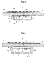
- Figure 3 shows a structure of the high-frequency transmitter-receiver apparatus according to another embodiment of the invention, in which the base plate 1 is divided separably into a mid portion 1-2 where the transceiver circuit is provided and a peripheral portion 1-1.
- the mid portion 1-2 should be so dimensioned that at least the transceiver component cover 5 can be mounted.
- FIG 4 shows in a sectional view another example of the structure of the high-frequency transmitter-receiver apparatus in which the transceiver component cover 5 is constituted by a side frame 5-2 and a cover sheet 5-1. Mounted at a location of the side frame 5-2 are pin terminals 12' for external connection, wherein the pin terminals 12' are electrically insulated by insulation material 8'. It can further be seen that the transceiver circuit is realized in a flip-chip package structure in which the MMIC semiconductor chip is mounted directly on the circuit substrate, as mentioned previously.
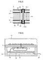
- FIG. 5 is a fragmentary sectional view showing on an enlarged scale the coaxial line (or coaxial cable, to say in another way) for electrically interconnecting the transceiver circuit and the antenna.
- Deposited on the antenna substrate 2 bonded onto the top surface of the base plate 1 are metal patterns 7 on antenna substrate and an ground conductor (or earth conductor) 21.
- metal patterns 10 on circuit substrate and a ground conductor (or earth conductor) 31 are deposited on the circuit substrate 3 which is bonded onto the bottom surface of the base plate 1.
- Electrical connection between the metal patterns 7 on antenna substrate and the metal patterns 10 on circuit substrate is established by means of the center conductor 6 supported by a dielectric 14 of the coaxial line and solders 13-1 and 13-2.
- the coaxial line of the structure in which glass, ceramic or the like may be employed as the dielectric 14 airtightness can easily be ensured for the high-frequency transmitter-receiver apparatus inclusive of the semiconductor chip.
- electrically conductive layers 23 and 33 may be deposited by plating or the like process on lateral surfaces of through-hole portions formed in the dielectric substrates (antenna substrate and circuit substrate) for inserting the center conductor therethrough.
- the electrically conductive layers 23 and 33 formed on the lateral surfaces of the through-hole portions mentioned above may be extended so as to form lands 22 and 32 flush with the ground conductors 21 and 31, respectively, which is effective for protecting the lateral surface conductive layers from delamination.
- the space defined between the dielectric substrate and the center conductor can be filled with solder essentially without any void owing to high-contact susceptibility of the metallic conductor and the solder.
- the high-frequency transmitter-receiver apparatus can be protected against deterioration of the characteristics even when the apparatus is employed in a vehicle-onboard radar system.
- the lateral surface conductive layers are provided, the current will flow along the solder surface and thus the loss due to roughness of the solder surface will not be negligible.
- the current can flow through the lateral surface conductive layers, whereby the electric loss can be suppressed to a minimum. Such advantageous effects can be observed especially in the millimeter wave region.
- soldering a metal such as AuSn, AuSi or the like can be used as well. Further, for the connection of the coaxial line, welding, ribbon bonding or the like may be resorted to in addition to the soldering.
- FIG. 6 is a sectional view of an antenna unit according to another embodiment of the present invention.
- the antenna unit according to the instant embodiment is comprised of a high-frequency transmitter-receiver apparatus or device described hereinbefore by reference Figs. 1 to 4 which is integrally combined with a signal processing circuit.
- a signal processing circuit substrate 17 on which circuit components 18 such as those for a power source circuit and an IF signal processing circuit are mounted is disposed in the vicinity of the high-frequency transmitter-receiver device, wherein the high-frequency transmitter-receiver device and the signal processing circuit are electrically interconnected by a lead wire 19.
- An antenna cover 16 formed of a dielectric is mounted so as to cover the whole antenna array while a cover 15 of signal processing circuit made of a metal and covering wholly the transceiver circuit and the signal processing circuit is mounted directly on the base plate 1, wherein signal transfers with external apparatuses are realized through the medium of a lead terminal 20 for external connection.
- a cover 15 of signal processing circuit made of a metal and covering wholly the transceiver circuit and the signal processing circuit is mounted directly on the base plate 1, wherein signal transfers with external apparatuses are realized through the medium of a lead terminal 20 for external connection.
- airtightness is not required because the circuit components 18 are packaged.
- Figure 7 is a sectional view showing a modified structure of the antenna unit shown in Fig. 6.
- this antenna unit some of the circuit components 18 for the IF signal processing circuit such as an operational amplifier and/or other is accommodated within the space defined by the transceiver component cover 5 mounted hermetically, wherein the IF signal is taken out externally from the transceiver component cover 5 after having been amplified (i.e., after the signal level of the IF signal has been raised).
- reference numeral 18-1 in Fig. 7 denotes the other parts or circuitries of the signal processing circuit.
- the amplified IF signal is outputted from the transceiver circuit packaged hermetically.
- the IF signal is less susceptible to the influence of noise generated by the other signal processing circuit components 18-1 including digital circuitries, which means that improved S/N ratio can be ensured, to an advantage.
- a vehicle-onboard radar system i.e., radar equipment for automobiles or motor vehicles
- a radar hereinafter referred to as the subject motor vehicle only for convenience of description
- Figure 19 is a pictorial view for illustrating schematically a configuration of such radar system.
- the radar system illustrated includes an antenna unit 151 designed for transmitting or sending out radio wave of millimeter-wave band and receiving echo returning from the fore-running motor vehicle or the obstacle to thereby detect difference between the frequency of the transmitted radio wave and that of the echo.
- the radio wave of the millimeter-wave band is less susceptible to the influence of weather conditions as compared with the infrared laser known heretofore and can thus ensure high accuracy for measurement of the inter-vehicle distance (i.e., distance between the fore-running motor vehicle and the subject motor vehicle).
- the relative running speed between the fore-running motor vehicle and the subject motor vehicle can be determined. Additionally, the inter-vehicle distance between the fore-running motor vehicle and the subject vehicle as well as the direction in which the fore-running motor vehicle is located, as viewed from the subject motor vehicle, can be detected.
- a signal processing unit 152 is provided for performing appropriate arithmetic processings on the output signal of the antenna unit 151 to thereby make decision as to the environmental situation for effectuating automatically controls required or desired for the subject motor vehicle such as throttle control, transmission control, brake control and/or the like.
- the ambient or environmental situations such as existence of obstacle, presence of a fore-running motor vehicle, relative speed between the fore-running motor vehicle and the subject motor vehicle should preferably be messaged to the operator or driver of the subject motor vehicle. Besides, an alarm should be issued to the driver as occasion requires.
- the signal processing unit 152 sends the relevant information to a driver display device 153 which is designed to execute relevant display processings and alarm message generating processing on the basis of the signals or information received from the signal processing unit 152.
- the signal processing unit and the antenna unit are provided discretely or separately from each other.
- both the signal processing unit and the antenna unit can be combined in a unitary structure by realizing the antenna unit in a miniaturized structure.
- integral combination of the signal processing unit and the antenna unit can facilitate mounting of the radar system on the motor vehicle or automobile.
- the antenna unit be mounted on the front or lateral side of the motor vehicle.
- the antenna unit should preferably be implemented in a small size at light weight.
- a high mechanical strength should be ensured for the antenna unit.
- Figure 8 is a sectional view showing a high-frequency transmitter-receiver apparatus which is designed for use in an antenna unit according to yet another embodiment of the present invention.
- the apparatus includes a base plate 101 (composed of sections 101-1 and 101-2) made of a metal and having a top surface on which an antenna substrate 102 formed of a dielectric for constituting an antenna is bonded and a bottom surface on which a circuit substrate 103 formed of a dielectric for constituting a transceiver circuit and an MMIC semiconductor chip 104 are mounted by bonding.
- Metal patterns 110 on circuit substrate deposited on the surface of the circuit substrate 103 and metal patterns 107 on antenna substrate deposited on the surface of the antenna substrate 102 are electrically connected to each other by an RF (radio frequency) coaxial line which is realized by a dielectric 114 and a metal center conductor 106. Since the MMIC semiconductor chip is not packaged, the transceiver circuit is hermetically sealed by means of a cover 105 of transceiver components made of a metal. The metal patterns 110 on circuit substrate and the semiconductor chips 104 are electrically interconnected by bonding wires 111. Parenthetically, the MMIC semiconductor chip 104 may be implemented in a so-called flip-chip package structure in which the MMIC semiconductor chip 104 is directly contacted onto the circuit substrate 103. Further, the base plate 101 and the transceiver component cover 105 may be formed of a nonmetallic material such as plastic or the like with the surface thereof being coated with metal through plating, evaporation or the like process.
- the base plate 101 is divided separately into a peripheral portion 101-1 where the transceiver circuit is provided and a mid portion 101-2.
- the mid portion 101-2 should be so dimensioned as to include at least the area which is hermetically sealed by the transceiver component cover 105.
- a connecting terminal of a coaxial structure which is composed of a metal conductor 108-1 for the terminal and a dielectric 108-2 for the terminal and which serves as the power supplying terminal (D.C. bias supply terminal) and/or the IF (intermediate frequency) signal terminal.
- the mid portion 101-2 of the base plate is partially recessed in the surface on which the antenna substrate is bonded, as illustrated in Figs. 10A and 10B.
- the metal conductor 108-1 for the terminal is electrically connected to the lead wire 109 forming the terminal for external connection to be thereby connected to an external power supply circuit or a signal processing circuit also provided externally.
- the high-frequency transmitter-receiver apparatus is equipped with two antennas, i.e., transmitting antenna and receiving antenna, there are required two coaxial terminals for interconnecting the transceiver circuit and these two antennas.
- the D.C. bias supply terminal or power supply terminal and the IF signal terminal are provided at one side of the housing, they may be provided at both sides. Of course, the invention is never restricted to any specific number of the terminals.
- Figure 9 is a bottom plan view of the high-frequency transmitter-receiver apparatus according to the instant embodiment of the invention, in which the antenna substrate 102 bonded onto the top surface of the base plate is indicated by a phantom line.
- Figures 10A and 10B show a structure of the mid portion 101-2 of the base plate according to an embodiment of the invention, in which Fig. 10A is a top plan view of the mid portion 101-2, and Fig. 10B is a sectional view of the same taken along a line A-B shown in Fig. 10A.
- numeral 106 i denotes a through-hole for the coaxial line interconnecting the transceiver circuit and the antenna
- numeral 108 denotes through-holes for the coaxial terminals for the D.C. bias supply or power supply and the IF signal.
- the surface I of the mid portion 101-2 onto which the antenna substrate is bonded is partially recessed for accommodating signal lines extending from the coaxial terminal.
- Figure 11 is a partially enlarged sectional view for illustrating a structure around the coaxial terminal (i.e., terminal of the coaxial structure).
- the dielectric substrate 103 constituting a part of the transceiver circuit is bonded onto the bottom surface of the mid portion 101-2 of the base plate.
- the through-hole 108 is formed in the dielectric substrate 103, and one end portion of the metal conductor 108-1 of the coaxial terminal is inserted into the through-hole to be subsequently connected to the pattern conductor of the transceiver circuit by soldering, as designated by numeral 112.
- the other end of the metal conductor 108-1 is connected to the lead wire (external terminal) 109 covered with an insulation coat.
- the lead wire 109 is connected to the signal processing circuit provided externally.
- a flat cable or the like available commercially can be made use of as the lead wires.
- the dielectric 108-2 supporting the metal conductor 108-1 of the coaxial terminal may serve for electrical insulation. By using ceramic or glass as the dielectric 108-2, airtightness of the transceiver circuit can be enhanced with the reliability thereof being enhanced.
- the lateral surface of the through-hole formed in the dielectric substrate 103 is coated with an electrically conductive layer through plating or the like process.
- the space defined between the dielectric substrate and the center conductor can be filled with solder without voids owing to the high contact susceptibility or affinity between the metal conductor and the solder, whereby the mechanical strength can be increased.
- Figure 12 is a view showing a structure of the coaxial terminal according to still another embodiment of the invention.
- one end portion of the metal conductor 108-1 is elongated so that the metal conductor 108-1 can serve as a lead wire for connection to the signal processing circuit provided externally, while the other end portion of the metal conductor 108-1 is connected to the pattern conductor of the transceiver circuit by a bonding wire.
- the coaxial terminal formed by using a metallic sleeve 113 of Kovar, iron or the like is provided separately to be connected to the mid portion 101-2 of the base plate by soldering or the like.
- Figure 13 is a sectional view of a high-frequency transmitter-receiver apparatus according to a further embodiment of the present invention. More specifically, the instant embodiment of the invention is directed to a structure of the high-frequency transmitter-receiver apparatus in which the mechanical strength as required can be sustained only by the antenna substrate because the area for the antenna is not excessively large or because the antenna substrate is thick.
- the base plate is not divided into the peripheral portion 101-1 and the mid portion 101-2, and the antenna substrate 102 is directly mounted on the base plate 1 in a region corresponding to the mid portion 101-2.
- Figure 14 is a sectional view of a high-frequency transmitter-receiver apparatus of a structure in which an transmitting antenna and a receiving antenna are provided separately from each other according to another embodiment of the present invention.
- the power supplying terminal and the terminal for the IF signal are provided at right and left end portions, respectively, as viewed in the figure, wherein high-frequency (RF) coaxial lines 106-1 and 106-2 for establishing connection between the antenna pattern conductors (metal patterns) and the high-frequency circuit pattern conductor (metal patterns) are provided discretely at two locations, i.e., at left-hand and right-hand sides, as viewed in the figure.
- RF radio frequency
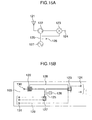
- FIGS 15A and 15B show yet another structure of the high-frequency transmitter-receiver apparatus according to an embodiment of the invention in which an antenna is employed common to transmission and reception
- Fig. 15A is a circuit diagram of a high-frequency (RF) circuit arrangement
- Fig. 15B shows an RF circuit pattern provided on a dielectric substrate 103.
- an RF (radio frequency) signal generated by an oscillator 127 is fed to an antenna 121 via a circulator 122. Since the antenna 121 is used for signal transmission and reception, the received RF signal, i.e., echo signal, is applied to the mixer 123 via the circulator 122.
- RF radio frequency
- the RF signal generated by the oscillator 127 is supplied to the mixer 123 as a local oscillation signal via a coupler 125, whereby the received RF signal or echo is converted into an IF (intermediate frequency) signal, which is taken out from an IF signal terminal 124.
- a resistor 126 serves to stably operate the coupler 125.
- the RF signal generated by the oscillator 127 implemented in the form of an MMIC semiconductor chip is applied to an RF coaxial terminal 130 which interconnects the RF circuit and the antenna through a microstrip line 128 and the circulator 122.
- a D.C. power or D.C. bias from the D.C. bias supply terminals 131 through a D.C. bias supply line 129 (shown by a phantom line) deposited on the dielectric substrate 103.
- the D.C. bias supply terminals 131 and the IF signal terminals 124 should preferably be disposed at locations in the vicinity of opposite sides (right and left sides as viewed in the figure) of the dielectric substrate 103, respectively, so that the IF signal lines and the D.C. bias supply lines do not extend in parallel.
- the IF signal may undergo interference by the noise carried by the D.C. bias supply line.
- a ground conductor earth conductor
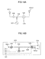
- FIGS. 16A and 16B show a structure of the high-frequency transmitter-receiver apparatus according to another embodiment of the invention in which a transmitting antenna and a receiving antenna are provided separately from each other, wherein Figs. 16A is a circuit diagram showing a high-frequency (RF) circuit arrangement and Fig. 16B shows a corresponding RF circuit pattern.
- RF radio frequency
- a part of the RF signal generated by the oscillator 127 is also supplied to the mixer 123 as a local oscillation signal via the distributor 134.
- the RF signal outputted from the oscillator 127 which is realized in the form of an MMIC semiconductor chip is supplied through a microstrip line 128 to an RF coaxial terminal 130-1 interconnecting the RF circuit and the transmitting antenna, while the signal received by the receiving antenna is applied to the mixer 123 implemented in the form of an MMIC semiconductor chip via an RF coaxial terminal 130-2.
- Figure 17A and 17B show a high-frequency transmitter-receiver apparatus according to still another embodiment of the present invention in which the transmitting antenna and the receiving antenna are provided separately from each other and in which a plurality of receiving antennas are provided in order to catch with high accuracy the direction in which a fore-running motor vehicle and/or obstacle exists. More specifically, Fig. 17A shows an exemplary RF circuit arrangement while Fig. 17B shows a corresponding RF circuit pattern. Referring to Fig. 17A, an RF signal generated by an oscillator 127 is sent out from a transmitting antenna 121-1 through an RF amplifier 133 via a distributor 134-1.
- the RF echoes as received by a plurality of transmitting receiving antennas 121-2 and 121-3 are supplied to mixers 123-1; 123-2. Additionally, a part of the RF signal generated by the oscillator 127 is also supplied to the mixers 123-1 and 123-2 as a local oscillation signal via distributors 134-1 and 134-2, respectively. Referring to Fig.
- the RF signal outputted from the oscillator 127 which is realized in the form of a semiconductor chip is supplied through a microstrip line 128 to an RF coaxial terminal 130-1 interconnecting the RF circuit and the transmitting antennas, while the echoes received by the receiving antennas are applied to the mixers 123-1 and 123-2 each implemented in the form of a semiconductor chip via RF coaxial terminals 130-2 and 130-3, respectively.
- the IF signal terminals 124 and the D.C. bias supply terminals 131 are provided at locations near to the opposite sides of the dielectric substrate 103, respectively, to thereby prevent the IF signal lines and the D.C. bias supply lines from extending in parallel.
- the efficiency of work involved in assembling the high-frequency transmitter-receiver apparatus can be enhanced while ensuring airtightness thereof by virtue of such arrangement that the coaxial terminal which may have a same structure as the coaxial line interconnecting the transceiver circuit and the antenna is used as the connecting terminal for electrically interconnecting the transceiver circuit and the external terminal.
Applications Claiming Priority (4)
| Application Number | Priority Date | Filing Date | Title |
|---|---|---|---|
| JP22400698 | 1998-08-07 | ||
| JP10224006A JP2000059140A (ja) | 1998-08-07 | 1998-08-07 | 高周波送受信装置 |
| JP494999 | 1999-01-12 | ||
| JP00494999A JP3758397B2 (ja) | 1999-01-12 | 1999-01-12 | 高周波送受信装置および車載レーダシステム |
Publications (2)
| Publication Number | Publication Date |
|---|---|
| EP0978729A2 true EP0978729A2 (de) | 2000-02-09 |
| EP0978729A3 EP0978729A3 (de) | 2002-03-20 |
Family
ID=26338814
Family Applications (1)
| Application Number | Title | Priority Date | Filing Date |
|---|---|---|---|
| EP99306230A Withdrawn EP0978729A3 (de) | 1998-08-07 | 1999-08-05 | Hochfrequenz-Sende-Empfangsvorrichtung für Fahrzeug-Radarsysteme |
Country Status (2)
| Country | Link |
|---|---|
| US (1) | US6249242B1 (de) |
| EP (1) | EP0978729A3 (de) |
Cited By (34)
| Publication number | Priority date | Publication date | Assignee | Title |
|---|---|---|---|---|
| US6249242B1 (en) * | 1998-08-07 | 2001-06-19 | Hitachi, Ltd. | High-frequency transmitter-receiver apparatus for such an application as vehicle-onboard radar system |
| FR2808886A1 (fr) * | 2000-05-15 | 2001-11-16 | Hitachi Ltd | Radar a ondes radioelectriques monte sur vehicule |
| WO2002009234A2 (en) * | 2000-07-21 | 2002-01-31 | Raytheon Company | Antenna structure and associated method |
| WO2002015323A2 (en) * | 2000-08-16 | 2002-02-21 | Raytheon Company | Highly integrated single substrate mmw multi-beam sensor |
| US6489927B2 (en) | 2000-08-16 | 2002-12-03 | Raytheon Company | System and technique for mounting a radar system on a vehicle |
| EP1280225A2 (de) * | 2001-07-23 | 2003-01-29 | Hitachi Ltd. | Hochfrequenz-Sender/Empfänger |
| WO2003041117A2 (de) * | 2001-11-09 | 2003-05-15 | Robert Bosch Gmbh | Integrirertes halbleiterbauelement für hochfrequenzmessungen und dessen verwendung |
| WO2003040754A1 (fr) * | 2001-11-09 | 2003-05-15 | Hitachi, Ltd. | Radar mobile a onde millimetrique |
| US6657581B1 (en) | 2000-08-16 | 2003-12-02 | Raytheon Company | Automotive lane changing aid indicator |
| EP1411369A1 (de) * | 2002-10-16 | 2004-04-21 | Valeo Schalter und Sensoren GmbH | Radarempfänger und Herstellungsverfahren für einen solchen Radar |
| EP1410062A2 (de) * | 2001-02-03 | 2004-04-21 | Robert Bosch Gmbh | Integrierte schaltung für ein radargerät in hermetisch abgeschlossenem gehäuse mit einer aus einem blech-biegeteil geformten patch-antenne |
| EP1422534A1 (de) * | 2002-10-10 | 2004-05-26 | Hitachi, Ltd. | Fahrzeugmontiertes Millimeterwellenradargerät, Millimeterwellenradarmodul und Herstellungsverfahren hiervon |
| US6748312B2 (en) | 2000-08-16 | 2004-06-08 | Raytheon Company | Safe distance algorithm for adaptive cruise control |
| FR2849927A1 (fr) * | 2003-01-13 | 2004-07-16 | Epcos Ag | Emetteur-recepteur radar pour des applications en micro-ondes et en ondes millimetriques |
| EP1438702A1 (de) * | 2001-09-27 | 2004-07-21 | Wavetronix LLC | Fahrzeugverkehrssensor |
| US6784828B2 (en) | 2000-08-16 | 2004-08-31 | Raytheon Company | Near object detection system |
| US6816107B2 (en) | 2000-08-16 | 2004-11-09 | Raytheon Company | Technique for changing a range gate and radar coverage |
| WO2005057728A1 (en) * | 2003-12-12 | 2005-06-23 | Stichting Noble House | Coupling for patch antennas |
| WO2005109330A1 (en) * | 2004-05-06 | 2005-11-17 | Fractus, S.A. | Radio-frequency system in package including antenna |
| EP1655803A1 (de) * | 2004-11-05 | 2006-05-10 | Hitachi, Ltd. | Hochfrequenzantenneanordnung und Verfahren für deren Herstellung |
| US7095372B2 (en) | 2002-11-07 | 2006-08-22 | Fractus, S.A. | Integrated circuit package including miniature antenna |
| WO2007017352A1 (de) * | 2005-08-11 | 2007-02-15 | Robert Bosch Gmbh | Radarsensor in kompaktbauweise |
| EP1907878A1 (de) * | 2005-07-18 | 2008-04-09 | Dan Manor | Antennen- bzw. sender/empfänger-konfiguration in einem verkehrssensor |
| WO2009142983A1 (en) * | 2008-05-23 | 2009-11-26 | Alliant Techsystems Inc. | Broadband patch antenna and antenna system |
| US7924226B2 (en) | 2004-09-27 | 2011-04-12 | Fractus, S.A. | Tunable antenna |
| US8196829B2 (en) | 2006-06-23 | 2012-06-12 | Fractus, S.A. | Chip module, sim card, wireless device and wireless communication method |
| US8330259B2 (en) | 2004-07-23 | 2012-12-11 | Fractus, S.A. | Antenna in package with reduced electromagnetic interaction with on chip elements |
| CN103207384A (zh) * | 2012-01-17 | 2013-07-17 | 万都株式会社 | 雷达装置及其装配方法 |
| CN103217684A (zh) * | 2012-01-19 | 2013-07-24 | 万都株式会社 | 雷达装置和天线装置 |
| CN103308906A (zh) * | 2012-03-08 | 2013-09-18 | 万都株式会社 | 雷达装置 |
| CN103389491A (zh) * | 2012-05-09 | 2013-11-13 | 万都株式会社 | 一种雷达装置和一种天线装置 |
| WO2017209761A1 (en) | 2016-06-03 | 2017-12-07 | Intel IP Corporation | Wireless module with antenna package and cap package |
| US10049569B2 (en) | 2005-10-31 | 2018-08-14 | Wavetronix Llc | Detecting roadway targets within a multiple beam radar system |
| EP4130783A1 (de) * | 2021-08-06 | 2023-02-08 | Aptiv Technologies Limited | Radarsystem für ein fahrzeug |
Families Citing this family (59)
| Publication number | Priority date | Publication date | Assignee | Title |
|---|---|---|---|---|
| WO2000017813A1 (fr) * | 1998-09-18 | 2000-03-30 | Hitachi Maxell, Ltd. | Dispositif de communication a semi-conducteurs sans contact |
| US6577269B2 (en) | 2000-08-16 | 2003-06-10 | Raytheon Company | Radar detection method and apparatus |
| EP1310018B1 (de) | 2000-08-16 | 2018-07-25 | Valeo Radar Systems, Inc. | Antennenarchitektur mit geschalteten strahlungskeulen |
| US6675094B2 (en) | 2000-09-08 | 2004-01-06 | Raytheon Company | Path prediction system and method |
| DE10104377A1 (de) * | 2001-02-01 | 2002-08-08 | Reitter & Schefenacker Gmbh | Betätigungsvorrichtung für Entriegelungseinrichtungen von Fahrzeugen, vorzugsweise von Kraftfahrzeugen |
| US6708100B2 (en) | 2001-03-14 | 2004-03-16 | Raytheon Company | Safe distance algorithm for adaptive cruise control |
| US6627992B2 (en) * | 2001-05-21 | 2003-09-30 | Xytrans, Inc. | Millimeter wave (MMW) transceiver module with transmitter, receiver and local oscillator frequency multiplier surface mounted chip set |
| US6563456B1 (en) * | 2001-10-04 | 2003-05-13 | Yazaki North America, Inc. | Flexible wave guide joint |
| JP3973402B2 (ja) * | 2001-10-25 | 2007-09-12 | 株式会社日立製作所 | 高周波回路モジュール |
| JP3883847B2 (ja) * | 2001-11-19 | 2007-02-21 | 株式会社日立製作所 | 車載用信号処理装置 |
| US6480144B1 (en) * | 2002-01-30 | 2002-11-12 | Ford Global Technologies, Inc. | Wireless communication between countermeasure devices |
| US20030190903A1 (en) * | 2002-07-22 | 2003-10-09 | Envara Ltd. | Zero-loss front end for wireless communication |
| JP3956823B2 (ja) * | 2002-10-07 | 2007-08-08 | 株式会社日本自動車部品総合研究所 | アンテナの実装方法、アンテナの実装構造、およびモニタ装置 |
| JP2004297486A (ja) * | 2003-03-27 | 2004-10-21 | Sharp Corp | 低雑音ブロックダウンコンバータ用多層基板 |
| US7391372B2 (en) * | 2003-06-26 | 2008-06-24 | Hrl Laboratories, Llc | Integrated phased array antenna |
| US8144059B2 (en) * | 2003-06-26 | 2012-03-27 | Hrl Laboratories, Llc | Active dielectric resonator antenna |
| CN100337365C (zh) * | 2003-11-20 | 2007-09-12 | 启碁科技股份有限公司 | 讯号接受装置 |
| JP2005348032A (ja) * | 2004-06-02 | 2005-12-15 | Yokohama Rubber Co Ltd:The | 車載用通信アンテナ |
| DE102004036890A1 (de) * | 2004-07-19 | 2006-02-16 | Würth Elektronik Rot am See GmbH & Co. KG | Leiterplattenanordnung |
| US7680464B2 (en) * | 2004-12-30 | 2010-03-16 | Valeo Radar Systems, Inc. | Waveguide—printed wiring board (PWB) interconnection |
| US7603097B2 (en) * | 2004-12-30 | 2009-10-13 | Valeo Radar Systems, Inc. | Vehicle radar sensor assembly |
| US20060160500A1 (en) * | 2005-01-14 | 2006-07-20 | Xytrans, Inc. | VSAT block up converter (BUC) chip |
| US7692598B1 (en) * | 2005-10-26 | 2010-04-06 | Niitek, Inc. | Method and apparatus for transmitting and receiving time-domain radar signals |
| US8248272B2 (en) | 2005-10-31 | 2012-08-21 | Wavetronix | Detecting targets in roadway intersections |
| JP4908899B2 (ja) * | 2006-04-07 | 2012-04-04 | ラピスセミコンダクタ株式会社 | 半導体装置及びその製造方法 |
| US7652619B1 (en) | 2007-05-25 | 2010-01-26 | Niitek, Inc. | Systems and methods using multiple down-conversion ratios in acquisition windows |
| US7649492B2 (en) * | 2007-05-25 | 2010-01-19 | Niitek, Inc. | Systems and methods for providing delayed signals |
| US9316729B2 (en) * | 2007-05-25 | 2016-04-19 | Niitek, Inc. | Systems and methods for providing trigger timing |
| US7675454B2 (en) * | 2007-09-07 | 2010-03-09 | Niitek, Inc. | System, method, and computer program product providing three-dimensional visualization of ground penetrating radar data |
| US8207885B2 (en) * | 2007-09-19 | 2012-06-26 | Niitek, Inc. | Adjustable pulse width ground penetrating radar |
| JP4656121B2 (ja) * | 2007-10-19 | 2011-03-23 | 株式会社デンソー | レーダ装置、および保持部材 |
| JP2009103458A (ja) * | 2007-10-19 | 2009-05-14 | Denso Corp | レーダ出力最適化方法、およびレーダ出力最適化装置 |
| JP4497190B2 (ja) * | 2007-10-19 | 2010-07-07 | 株式会社デンソー | レーダ装置、および保持部材 |
| US8022861B2 (en) * | 2008-04-04 | 2011-09-20 | Toyota Motor Engineering & Manufacturing North America, Inc. | Dual-band antenna array and RF front-end for mm-wave imager and radar |
| US7830301B2 (en) * | 2008-04-04 | 2010-11-09 | Toyota Motor Engineering & Manufacturing North America, Inc. | Dual-band antenna array and RF front-end for automotive radars |
| US7733265B2 (en) * | 2008-04-04 | 2010-06-08 | Toyota Motor Engineering & Manufacturing North America, Inc. | Three dimensional integrated automotive radars and methods of manufacturing the same |
| US7990237B2 (en) * | 2009-01-16 | 2011-08-02 | Toyota Motor Engineering & Manufacturing North America, Inc. | System and method for improving performance of coplanar waveguide bends at mm-wave frequencies |
| US8013784B2 (en) * | 2009-03-03 | 2011-09-06 | Toyota Motor Engineering & Manufacturing North America, Inc. | Butler matrix for 3D integrated RF front-ends |
| US20110316139A1 (en) * | 2010-06-23 | 2011-12-29 | Broadcom Corporation | Package for a wireless enabled integrated circuit |
| US8786496B2 (en) | 2010-07-28 | 2014-07-22 | Toyota Motor Engineering & Manufacturing North America, Inc. | Three-dimensional array antenna on a substrate with enhanced backlobe suppression for mm-wave automotive applications |
| JP5172925B2 (ja) | 2010-09-24 | 2013-03-27 | 株式会社東芝 | 無線装置 |
| US20120086114A1 (en) * | 2010-10-07 | 2012-04-12 | Broadcom Corporation | Millimeter devices on an integrated circuit |
| US8901945B2 (en) | 2011-02-23 | 2014-12-02 | Broadcom Corporation | Test board for use with devices having wirelessly enabled functional blocks and method of using same |
| JP5414749B2 (ja) | 2011-07-13 | 2014-02-12 | 株式会社東芝 | 無線装置 |
| JP5417389B2 (ja) | 2011-07-13 | 2014-02-12 | 株式会社東芝 | 無線装置 |
| US8928139B2 (en) | 2011-09-30 | 2015-01-06 | Broadcom Corporation | Device having wirelessly enabled functional blocks |
| JP6121705B2 (ja) * | 2012-12-12 | 2017-04-26 | 株式会社東芝 | 無線装置 |
| US9412271B2 (en) | 2013-01-30 | 2016-08-09 | Wavetronix Llc | Traffic flow through an intersection by reducing platoon interference |
| DE102013211712A1 (de) * | 2013-06-20 | 2015-01-08 | Siemens Aktiengesellschaft | Antennenmodul und Vorrichtung mit Antennenmodul |
| US9153861B2 (en) * | 2013-08-07 | 2015-10-06 | GM Global Technology Operations LLC | Using a vehicle structure as a medium for communication and power distribution |
| US9653796B2 (en) | 2013-12-16 | 2017-05-16 | Valeo Radar Systems, Inc. | Structure and technique for antenna decoupling in a vehicle mounted sensor |
| JP2015145848A (ja) * | 2014-02-04 | 2015-08-13 | 古野電気株式会社 | レーダアンテナ |
| DE102014104944A1 (de) * | 2014-04-08 | 2015-10-08 | Hella Kgaa Hueck & Co. | Radarsensor |
| US9488719B2 (en) | 2014-05-30 | 2016-11-08 | Toyota Motor Engineering & Manufacturing North America, Inc. | Automotive radar sub-system packaging for robustness |
| WO2018037655A1 (ja) | 2016-08-24 | 2018-03-01 | 株式会社村田製作所 | アンテナモジュール |
| US11283190B2 (en) * | 2017-11-03 | 2022-03-22 | Avl Technologies, Inc. | Active fixed beam antenna array |
| EP3588673B1 (de) * | 2018-06-29 | 2024-04-03 | Advanced Automotive Antennas, S.L. | Unterdachantennenmodule für fahrzeuge |
| US10649585B1 (en) * | 2019-01-08 | 2020-05-12 | Nxp B.V. | Electric field sensor |
| CN113013583B (zh) * | 2021-01-29 | 2023-08-18 | 中国电子科技集团公司第三十八研究所 | 毫米波雷达封装模组 |
Citations (3)
| Publication number | Priority date | Publication date | Assignee | Title |
|---|---|---|---|---|
| US4462098A (en) * | 1982-02-16 | 1984-07-24 | Motorola, Inc. | Radio frequency signal combining/sorting apparatus |
| EP0843182A2 (de) * | 1996-11-18 | 1998-05-20 | Franco Baldi | Hindernis-Sensor mit Kollimation und Fokussierung des emmittierten Schalbes |
| US5874920A (en) * | 1996-01-26 | 1999-02-23 | Fujitsu Limited | Portable radio equipment, and built-in antenna mounting structure and shielding structure for the portable radio equipment |
Family Cites Families (13)
| Publication number | Priority date | Publication date | Assignee | Title |
|---|---|---|---|---|
| US3818386A (en) * | 1967-04-03 | 1974-06-18 | Texas Instruments Inc | Solid-state modular microwave system |
| JPS56126302A (en) * | 1980-03-10 | 1981-10-03 | Toshio Makimoto | Circular polarized wave microstrip line antenna |
| JPS59108404A (ja) * | 1982-12-14 | 1984-06-22 | Taiyo Musen Kk | 方向探知機の空中線装置 |
| US4635006A (en) * | 1984-12-18 | 1987-01-06 | Rca Corporation | Adjustable waveguide branch directional coupler |
| US5087920A (en) * | 1987-07-30 | 1992-02-11 | Sony Corporation | Microwave antenna |
| JPH0659009B2 (ja) * | 1988-03-10 | 1994-08-03 | 株式会社豊田中央研究所 | 移動体用アンテナ |
| US5432524A (en) * | 1993-03-01 | 1995-07-11 | Her Majesty The Queen In Right Of Canada, As Represented By The Minister Of Communications | Drive arrangement for mechanically-steered antennas |
| WO1995025387A1 (fr) * | 1994-03-17 | 1995-09-21 | Fujitsu Limited | Emetteur-recepteur a antenne |
| JPH08250913A (ja) * | 1995-03-15 | 1996-09-27 | Honda Motor Co Ltd | Mmicパッケージ組立 |
| ES2114717T3 (es) * | 1995-04-20 | 1998-06-01 | Fuba Automotive Gmbh | Disposicion de antenas planas. |
| US6008750A (en) * | 1997-02-11 | 1999-12-28 | Decatur Electronics, Inc. | Microwave transceiver utilizing a microstrip antenna |
| US5896107A (en) * | 1997-05-27 | 1999-04-20 | Allen Telecom Inc. | Dual polarized aperture coupled microstrip patch antenna system |
| EP0978729A3 (de) * | 1998-08-07 | 2002-03-20 | Hitachi, Ltd. | Hochfrequenz-Sende-Empfangsvorrichtung für Fahrzeug-Radarsysteme |
-
1999
- 1999-08-05 EP EP99306230A patent/EP0978729A3/de not_active Withdrawn
- 1999-08-06 US US09/369,400 patent/US6249242B1/en not_active Expired - Fee Related
Patent Citations (3)
| Publication number | Priority date | Publication date | Assignee | Title |
|---|---|---|---|---|
| US4462098A (en) * | 1982-02-16 | 1984-07-24 | Motorola, Inc. | Radio frequency signal combining/sorting apparatus |
| US5874920A (en) * | 1996-01-26 | 1999-02-23 | Fujitsu Limited | Portable radio equipment, and built-in antenna mounting structure and shielding structure for the portable radio equipment |
| EP0843182A2 (de) * | 1996-11-18 | 1998-05-20 | Franco Baldi | Hindernis-Sensor mit Kollimation und Fokussierung des emmittierten Schalbes |
Non-Patent Citations (1)
| Title |
|---|
| PATENT ABSTRACTS OF JAPAN vol. 1997, no. 01, 31 January 1997 (1997-01-31) & JP 08 250913 A (HONDA MOTOR CO LTD), 27 September 1996 (1996-09-27) * |
Cited By (73)
| Publication number | Priority date | Publication date | Assignee | Title |
|---|---|---|---|---|
| US6249242B1 (en) * | 1998-08-07 | 2001-06-19 | Hitachi, Ltd. | High-frequency transmitter-receiver apparatus for such an application as vehicle-onboard radar system |
| US6795013B2 (en) | 2000-05-15 | 2004-09-21 | Hitachi, Ltd. | Vehicle-mounted radio wave radar |
| FR2808886A1 (fr) * | 2000-05-15 | 2001-11-16 | Hitachi Ltd | Radar a ondes radioelectriques monte sur vehicule |
| WO2002009234A3 (en) * | 2000-07-21 | 2002-04-04 | Raytheon Co | Antenna structure and associated method |
| WO2002009234A2 (en) * | 2000-07-21 | 2002-01-31 | Raytheon Company | Antenna structure and associated method |
| US6816107B2 (en) | 2000-08-16 | 2004-11-09 | Raytheon Company | Technique for changing a range gate and radar coverage |
| US6489927B2 (en) | 2000-08-16 | 2002-12-03 | Raytheon Company | System and technique for mounting a radar system on a vehicle |
| US6501415B1 (en) | 2000-08-16 | 2002-12-31 | Raytheon Company | Highly integrated single substrate MMW multi-beam sensor |
| KR100831507B1 (ko) | 2000-08-16 | 2008-05-22 | 레이던 컴퍼니 | 고집적된 단일 기판 mmw 멀티빔 센서 |
| US6748312B2 (en) | 2000-08-16 | 2004-06-08 | Raytheon Company | Safe distance algorithm for adaptive cruise control |
| WO2002015323A2 (en) * | 2000-08-16 | 2002-02-21 | Raytheon Company | Highly integrated single substrate mmw multi-beam sensor |
| US6657581B1 (en) | 2000-08-16 | 2003-12-02 | Raytheon Company | Automotive lane changing aid indicator |
| US6784828B2 (en) | 2000-08-16 | 2004-08-31 | Raytheon Company | Near object detection system |
| WO2002015323A3 (en) * | 2000-08-16 | 2002-06-13 | Raytheon Co | Highly integrated single substrate mmw multi-beam sensor |
| EP1410062A2 (de) * | 2001-02-03 | 2004-04-21 | Robert Bosch Gmbh | Integrierte schaltung für ein radargerät in hermetisch abgeschlossenem gehäuse mit einer aus einem blech-biegeteil geformten patch-antenne |
| EP1280225A2 (de) * | 2001-07-23 | 2003-01-29 | Hitachi Ltd. | Hochfrequenz-Sender/Empfänger |
| EP1280225A3 (de) * | 2001-07-23 | 2003-06-11 | Hitachi Ltd. | Hochfrequenz-Sender/Empfänger |
| US6727853B2 (en) | 2001-07-23 | 2004-04-27 | Hitachi, Ltd. | High frequency transmitter-receiver |
| USRE48781E1 (en) | 2001-09-27 | 2021-10-19 | Wavetronix Llc | Vehicular traffic sensor |
| EP1438702A1 (de) * | 2001-09-27 | 2004-07-21 | Wavetronix LLC | Fahrzeugverkehrssensor |
| US7427930B2 (en) | 2001-09-27 | 2008-09-23 | Wavetronix Llc | Vehicular traffic sensor |
| EP1438702A4 (de) * | 2001-09-27 | 2005-05-11 | Wavetronix Llc | Fahrzeugverkehrssensor |
| EP1462822A4 (de) * | 2001-11-09 | 2009-09-23 | Hitachi Ltd | Mobiler millimeterwellenradar |
| US7109917B2 (en) | 2001-11-09 | 2006-09-19 | Robert Bosch Gmbh | Intergrated semiconductor component for high-frequency measurement and use thereof |
| WO2003041117A3 (de) * | 2001-11-09 | 2003-09-18 | Bosch Gmbh Robert | Integrirertes halbleiterbauelement für hochfrequenzmessungen und dessen verwendung |
| EP1462822A1 (de) * | 2001-11-09 | 2004-09-29 | Hitachi, Ltd. | Mobiler millimeterwellenradar |
| WO2003040754A1 (fr) * | 2001-11-09 | 2003-05-15 | Hitachi, Ltd. | Radar mobile a onde millimetrique |
| WO2003041117A2 (de) * | 2001-11-09 | 2003-05-15 | Robert Bosch Gmbh | Integrirertes halbleiterbauelement für hochfrequenzmessungen und dessen verwendung |
| EP1422534A1 (de) * | 2002-10-10 | 2004-05-26 | Hitachi, Ltd. | Fahrzeugmontiertes Millimeterwellenradargerät, Millimeterwellenradarmodul und Herstellungsverfahren hiervon |
| US7355547B2 (en) | 2002-10-10 | 2008-04-08 | Hitachi, Ltd. | Vehicle-mounted millimeter wave radar device, millimeter wave radar module, and manufacturing method thereof |
| US7098842B2 (en) | 2002-10-10 | 2006-08-29 | Hitachi, Ltd. | Vehicle-mounted millimeter wave radar device, millimeter wave radar module, and manufacturing method thereof |
| EP1411369A1 (de) * | 2002-10-16 | 2004-04-21 | Valeo Schalter und Sensoren GmbH | Radarempfänger und Herstellungsverfahren für einen solchen Radar |
| US10320079B2 (en) | 2002-11-07 | 2019-06-11 | Fractus, S.A. | Integrated circuit package including miniature antenna |
| US9077073B2 (en) | 2002-11-07 | 2015-07-07 | Fractus, S.A. | Integrated circuit package including miniature antenna |
| US10056691B2 (en) | 2002-11-07 | 2018-08-21 | Fractus, S.A. | Integrated circuit package including miniature antenna |
| US8203488B2 (en) | 2002-11-07 | 2012-06-19 | Fractus, S.A. | Integrated circuit package including miniature antenna |
| US9761948B2 (en) | 2002-11-07 | 2017-09-12 | Fractus, S.A. | Integrated circuit package including miniature antenna |
| US10644405B2 (en) | 2002-11-07 | 2020-05-05 | Fractus, S.A. | Integrated circuit package including miniature antenna |
| US7463199B2 (en) | 2002-11-07 | 2008-12-09 | Fractus, S.A. | Integrated circuit package including miniature antenna |
| US7095372B2 (en) | 2002-11-07 | 2006-08-22 | Fractus, S.A. | Integrated circuit package including miniature antenna |
| US7791539B2 (en) | 2002-11-07 | 2010-09-07 | Fractus, S.A. | Radio-frequency system in package including antenna |
| US8421686B2 (en) | 2002-11-07 | 2013-04-16 | Fractus, S.A. | Radio-frequency system in package including antenna |
| WO2004063767A1 (de) * | 2003-01-13 | 2004-07-29 | Epcos Ag | Radar-transceiver für mikrowellen- und millimeterwellenanwendungen |
| FR2849927A1 (fr) * | 2003-01-13 | 2004-07-16 | Epcos Ag | Emetteur-recepteur radar pour des applications en micro-ondes et en ondes millimetriques |
| WO2005057728A1 (en) * | 2003-12-12 | 2005-06-23 | Stichting Noble House | Coupling for patch antennas |
| US7868827B2 (en) | 2003-12-12 | 2011-01-11 | Stiching Noble House | Coupling for patch antennas |
| WO2005109330A1 (en) * | 2004-05-06 | 2005-11-17 | Fractus, S.A. | Radio-frequency system in package including antenna |
| US8330259B2 (en) | 2004-07-23 | 2012-12-11 | Fractus, S.A. | Antenna in package with reduced electromagnetic interaction with on chip elements |
| US7924226B2 (en) | 2004-09-27 | 2011-04-12 | Fractus, S.A. | Tunable antenna |
| EP1655803A1 (de) * | 2004-11-05 | 2006-05-10 | Hitachi, Ltd. | Hochfrequenzantenneanordnung und Verfahren für deren Herstellung |
| US7456790B2 (en) | 2004-11-05 | 2008-11-25 | Hitachi, Ltd. | High frequency antenna device and method of manufacturing the same, HF antenna printed circuit board for HF antenna device, and transmitting and receiving device using HF antenna device |
| EP1907878A1 (de) * | 2005-07-18 | 2008-04-09 | Dan Manor | Antennen- bzw. sender/empfänger-konfiguration in einem verkehrssensor |
| EP1907878A4 (de) * | 2005-07-18 | 2011-08-03 | Image Sensing Systems Inc | Antennen- bzw. sender/empfänger-konfiguration in einem verkehrssensor |
| WO2007017352A1 (de) * | 2005-08-11 | 2007-02-15 | Robert Bosch Gmbh | Radarsensor in kompaktbauweise |
| US10276041B2 (en) | 2005-10-31 | 2019-04-30 | Wavetronix Llc | Detecting roadway targets across beams |
| US10049569B2 (en) | 2005-10-31 | 2018-08-14 | Wavetronix Llc | Detecting roadway targets within a multiple beam radar system |
| US8196829B2 (en) | 2006-06-23 | 2012-06-12 | Fractus, S.A. | Chip module, sim card, wireless device and wireless communication method |
| WO2009142983A1 (en) * | 2008-05-23 | 2009-11-26 | Alliant Techsystems Inc. | Broadband patch antenna and antenna system |
| US8232924B2 (en) | 2008-05-23 | 2012-07-31 | Alliant Techsystems Inc. | Broadband patch antenna and antenna system |
| CN103207384A (zh) * | 2012-01-17 | 2013-07-17 | 万都株式会社 | 雷达装置及其装配方法 |
| US9261588B2 (en) | 2012-01-17 | 2016-02-16 | Mando Corporation | Radar apparatus and method manufacturing the same |
| CN103217684A (zh) * | 2012-01-19 | 2013-07-24 | 万都株式会社 | 雷达装置和天线装置 |
| CN103217684B (zh) * | 2012-01-19 | 2015-03-11 | 万都株式会社 | 雷达装置和天线装置 |
| CN103308906A (zh) * | 2012-03-08 | 2013-09-18 | 万都株式会社 | 雷达装置 |
| CN103308906B (zh) * | 2012-03-08 | 2016-01-20 | 万都株式会社 | 雷达装置 |
| US9207311B2 (en) | 2012-03-08 | 2015-12-08 | Mando Corporation | Radar apparatus |
| CN103389491A (zh) * | 2012-05-09 | 2013-11-13 | 万都株式会社 | 一种雷达装置和一种天线装置 |
| US9274216B2 (en) | 2012-05-09 | 2016-03-01 | Mando Corporation | Radar apparatus and an antenna apparatus |
| EP3465751A4 (de) * | 2016-06-03 | 2019-12-11 | Intel IP Corporation | Drahtlosmodul mit antennenpackung und kappenpackung |
| US10756033B2 (en) | 2016-06-03 | 2020-08-25 | Intel IP Corporation | Wireless module with antenna package and cap package |
| WO2017209761A1 (en) | 2016-06-03 | 2017-12-07 | Intel IP Corporation | Wireless module with antenna package and cap package |
| TWI766863B (zh) * | 2016-06-03 | 2022-06-11 | 美商英特爾公司 | 具有天線封裝及蓋封裝之無線模組 |
| EP4130783A1 (de) * | 2021-08-06 | 2023-02-08 | Aptiv Technologies Limited | Radarsystem für ein fahrzeug |
Also Published As
| Publication number | Publication date |
|---|---|
| EP0978729A3 (de) | 2002-03-20 |
| US6249242B1 (en) | 2001-06-19 |
Similar Documents
| Publication | Publication Date | Title |
|---|---|---|
| US6249242B1 (en) | High-frequency transmitter-receiver apparatus for such an application as vehicle-onboard radar system | |
| JP5707657B2 (ja) | 表面装着用の小型マイクロ波部品 | |
| JP4588073B2 (ja) | マイクロ波用途のための小型電子部品 | |
| US8179306B2 (en) | High-frequency circuit board, high-frequency circuit module, and radar apparatus | |
| JP3973402B2 (ja) | 高周波回路モジュール | |
| EP1777551A2 (de) | Millimeter-Radarwellenvorrichtung und Millimeter-Radarsystem | |
| US20080316126A1 (en) | Antenna System for a Radar Transceiver | |
| US6686867B1 (en) | Radar sensor and radar antenna for monitoring the environment of a motor vehicle | |
| JP5216848B2 (ja) | 高周波モジュールおよびその製造方法ならびに該高周波モジュールを備えた送信器、受信器、送受信器およびレーダ装置 | |
| US20200403298A1 (en) | Package integrated waveguide | |
| JPH1079623A (ja) | アンテナ素子を内蔵する半導体モジュール | |
| JP3801884B2 (ja) | 高周波送受信装置 | |
| JP2003315438A (ja) | レーダセンサ | |
| WO2003040754A1 (fr) | Radar mobile a onde millimetrique | |
| JP3758397B2 (ja) | 高周波送受信装置および車載レーダシステム | |
| US10199707B2 (en) | Ball-grid-array radio-frequency integrated-circuit printed-circuit-board assembly for automated vehicles | |
| JPH10233621A (ja) | アンテナ一体化マイクロ波・ミリ波回路 | |
| JP5179570B2 (ja) | 高周波モジュールおよびその製造方法ならびに該高周波モジュールを備えた送信器、受信器、送受信器およびレーダ装置 | |
| JPH10261917A (ja) | ミリ波送受信装置 | |
| CN101317103A (zh) | 用于雷达传感器的天线装置 | |
| JPH1117063A (ja) | 半導体チップ実装用回路基板、半導体チップ収納用パッケージ、及び半導体デバイス | |
| JP4745943B2 (ja) | 電子回路、送信器、受信器、送受信器 | |
| JP3800884B2 (ja) | 非接触icカードと移動体識別システム | |
| JP2011003651A (ja) | 回路装置、及び電子機器 | |
| JP2001244409A (ja) | 高周波モジュール |
Legal Events
| Date | Code | Title | Description |
|---|---|---|---|
| PUAI | Public reference made under article 153(3) epc to a published international application that has entered the european phase |
Free format text: ORIGINAL CODE: 0009012 |
|
| AK | Designated contracting states |
Kind code of ref document: A2 Designated state(s): AT BE CH CY DE DK ES FI FR GB GR IE IT LI LU MC NL PT SE Kind code of ref document: A2 Designated state(s): DE FR GB |
|
| AX | Request for extension of the european patent |
Free format text: AL;LT;LV;MK;RO;SI |
|
| PUAL | Search report despatched |
Free format text: ORIGINAL CODE: 0009013 |
|
| AK | Designated contracting states |
Kind code of ref document: A3 Designated state(s): AT BE CH CY DE DK ES FI FR GB GR IE IT LI LU MC NL PT SE |
|
| AX | Request for extension of the european patent |
Free format text: AL;LT;LV;MK;RO;SI |
|
| RIC1 | Information provided on ipc code assigned before grant |
Free format text: 7G 01S 7/03 A, 7G 01S 13/93 B |
|
| 17P | Request for examination filed |
Effective date: 20020620 |
|
| AKX | Designation fees paid |
Free format text: DE FR GB |
|
| 17Q | First examination report despatched |
Effective date: 20061110 |
|
| STAA | Information on the status of an ep patent application or granted ep patent |
Free format text: STATUS: THE APPLICATION IS DEEMED TO BE WITHDRAWN |
|
| 18D | Application deemed to be withdrawn |
Effective date: 20070522 |