EP0977469B1 - Improved transparent, flexible permeability barrier for organic electroluminescent devices - Google Patents
Improved transparent, flexible permeability barrier for organic electroluminescent devices Download PDFInfo
- Publication number
- EP0977469B1 EP0977469B1 EP99114946A EP99114946A EP0977469B1 EP 0977469 B1 EP0977469 B1 EP 0977469B1 EP 99114946 A EP99114946 A EP 99114946A EP 99114946 A EP99114946 A EP 99114946A EP 0977469 B1 EP0977469 B1 EP 0977469B1
- Authority
- EP
- European Patent Office
- Prior art keywords
- layer
- water
- polymer
- barrier
- oxide
- Prior art date
- Legal status (The legal status is an assumption and is not a legal conclusion. Google has not performed a legal analysis and makes no representation as to the accuracy of the status listed.)
- Expired - Lifetime
Links
- 230000004888 barrier function Effects 0.000 title claims description 25
- 230000035699 permeability Effects 0.000 title description 8
- 229920000642 polymer Polymers 0.000 claims description 36
- XLYOFNOQVPJJNP-UHFFFAOYSA-N water Substances O XLYOFNOQVPJJNP-UHFFFAOYSA-N 0.000 claims description 33
- QVGXLLKOCUKJST-UHFFFAOYSA-N atomic oxygen Chemical compound [O] QVGXLLKOCUKJST-UHFFFAOYSA-N 0.000 claims description 30
- 239000001301 oxygen Substances 0.000 claims description 30
- 229910052760 oxygen Inorganic materials 0.000 claims description 30
- 238000000034 method Methods 0.000 claims description 24
- 239000000463 material Substances 0.000 claims description 17
- 238000000151 deposition Methods 0.000 claims description 14
- 150000004767 nitrides Chemical class 0.000 claims description 12
- 229910052751 metal Inorganic materials 0.000 claims description 9
- 239000002184 metal Substances 0.000 claims description 9
- 238000010521 absorption reaction Methods 0.000 claims description 6
- 238000000623 plasma-assisted chemical vapour deposition Methods 0.000 claims description 6
- 229910052581 Si3N4 Inorganic materials 0.000 claims description 5
- HQVNEWCFYHHQES-UHFFFAOYSA-N silicon nitride Chemical compound N12[Si]34N5[Si]62N3[Si]51N64 HQVNEWCFYHHQES-UHFFFAOYSA-N 0.000 claims description 5
- VYPSYNLAJGMNEJ-UHFFFAOYSA-N Silicium dioxide Chemical compound O=[Si]=O VYPSYNLAJGMNEJ-UHFFFAOYSA-N 0.000 claims description 4
- TWNQGVIAIRXVLR-UHFFFAOYSA-N oxo(oxoalumanyloxy)alumane Chemical compound O=[Al]O[Al]=O TWNQGVIAIRXVLR-UHFFFAOYSA-N 0.000 claims description 4
- XUIMIQQOPSSXEZ-UHFFFAOYSA-N Silicon Chemical compound [Si] XUIMIQQOPSSXEZ-UHFFFAOYSA-N 0.000 claims description 3
- PMHQVHHXPFUNSP-UHFFFAOYSA-M copper(1+);methylsulfanylmethane;bromide Chemical compound Br[Cu].CSC PMHQVHHXPFUNSP-UHFFFAOYSA-M 0.000 claims description 3
- 229910052710 silicon Inorganic materials 0.000 claims description 3
- 239000010703 silicon Substances 0.000 claims description 3
- 229910052814 silicon oxide Inorganic materials 0.000 claims 2
- 239000011358 absorbing material Substances 0.000 claims 1
- 229910010272 inorganic material Inorganic materials 0.000 claims 1
- 239000011147 inorganic material Substances 0.000 claims 1
- 239000011368 organic material Substances 0.000 claims 1
- 239000010410 layer Substances 0.000 description 75
- 239000000758 substrate Substances 0.000 description 14
- 210000002381 plasma Anatomy 0.000 description 11
- 238000005538 encapsulation Methods 0.000 description 8
- 239000000178 monomer Substances 0.000 description 8
- 238000000576 coating method Methods 0.000 description 7
- 230000008021 deposition Effects 0.000 description 7
- 229910052791 calcium Inorganic materials 0.000 description 6
- 239000011575 calcium Substances 0.000 description 6
- 239000011248 coating agent Substances 0.000 description 6
- 229920000139 polyethylene terephthalate Polymers 0.000 description 6
- 239000005020 polyethylene terephthalate Substances 0.000 description 6
- 238000012545 processing Methods 0.000 description 6
- OYPRJOBELJOOCE-UHFFFAOYSA-N Calcium Chemical compound [Ca] OYPRJOBELJOOCE-UHFFFAOYSA-N 0.000 description 5
- 238000006243 chemical reaction Methods 0.000 description 5
- 238000002347 injection Methods 0.000 description 4
- 239000007924 injection Substances 0.000 description 4
- 239000012044 organic layer Substances 0.000 description 4
- WHXSMMKQMYFTQS-UHFFFAOYSA-N Lithium Chemical compound [Li] WHXSMMKQMYFTQS-UHFFFAOYSA-N 0.000 description 3
- 230000008901 benefit Effects 0.000 description 3
- 238000005516 engineering process Methods 0.000 description 3
- 238000001704 evaporation Methods 0.000 description 3
- 150000002500 ions Chemical class 0.000 description 3
- 229910052744 lithium Inorganic materials 0.000 description 3
- 229910052749 magnesium Inorganic materials 0.000 description 3
- 239000011777 magnesium Substances 0.000 description 3
- 238000004544 sputter deposition Methods 0.000 description 3
- KUDUQBURMYMBIJ-UHFFFAOYSA-N 2-prop-2-enoyloxyethyl prop-2-enoate Chemical compound C=CC(=O)OCCOC(=O)C=C KUDUQBURMYMBIJ-UHFFFAOYSA-N 0.000 description 2
- XKRFYHLGVUSROY-UHFFFAOYSA-N Argon Chemical compound [Ar] XKRFYHLGVUSROY-UHFFFAOYSA-N 0.000 description 2
- IJGRMHOSHXDMSA-UHFFFAOYSA-N Atomic nitrogen Chemical compound N#N IJGRMHOSHXDMSA-UHFFFAOYSA-N 0.000 description 2
- FYYHWMGAXLPEAU-UHFFFAOYSA-N Magnesium Chemical compound [Mg] FYYHWMGAXLPEAU-UHFFFAOYSA-N 0.000 description 2
- -1 Poly(ethylene terephthalate) Polymers 0.000 description 2
- NIXOWILDQLNWCW-UHFFFAOYSA-N acrylic acid group Chemical group C(C=C)(=O)O NIXOWILDQLNWCW-UHFFFAOYSA-N 0.000 description 2
- 150000001875 compounds Chemical class 0.000 description 2
- 230000007547 defect Effects 0.000 description 2
- 239000003989 dielectric material Substances 0.000 description 2
- 230000004907 flux Effects 0.000 description 2
- 239000007789 gas Substances 0.000 description 2
- 229910052809 inorganic oxide Inorganic materials 0.000 description 2
- 239000007788 liquid Substances 0.000 description 2
- 238000004519 manufacturing process Methods 0.000 description 2
- 150000002739 metals Chemical class 0.000 description 2
- 230000000149 penetrating effect Effects 0.000 description 2
- 239000000243 solution Substances 0.000 description 2
- PNEYBMLMFCGWSK-UHFFFAOYSA-N Alumina Chemical class [O-2].[O-2].[O-2].[Al+3].[Al+3] PNEYBMLMFCGWSK-UHFFFAOYSA-N 0.000 description 1
- BSYNRYMUTXBXSQ-UHFFFAOYSA-N Aspirin Chemical compound CC(=O)OC1=CC=CC=C1C(O)=O BSYNRYMUTXBXSQ-UHFFFAOYSA-N 0.000 description 1
- 229920002799 BoPET Polymers 0.000 description 1
- VVQNEPGJFQJSBK-UHFFFAOYSA-N Methyl methacrylate Chemical compound COC(=O)C(C)=C VVQNEPGJFQJSBK-UHFFFAOYSA-N 0.000 description 1
- BLRPTPMANUNPDV-UHFFFAOYSA-N Silane Chemical compound [SiH4] BLRPTPMANUNPDV-UHFFFAOYSA-N 0.000 description 1
- 150000001252 acrylic acid derivatives Chemical class 0.000 description 1
- 229910052783 alkali metal Inorganic materials 0.000 description 1
- 150000001340 alkali metals Chemical class 0.000 description 1
- 150000001336 alkenes Chemical class 0.000 description 1
- 229910052786 argon Inorganic materials 0.000 description 1
- 238000009835 boiling Methods 0.000 description 1
- 150000004649 carbonic acid derivatives Chemical class 0.000 description 1
- 239000010406 cathode material Substances 0.000 description 1
- 238000010549 co-Evaporation Methods 0.000 description 1
- 239000003086 colorant Substances 0.000 description 1
- 239000004020 conductor Substances 0.000 description 1
- 238000001816 cooling Methods 0.000 description 1
- 230000008878 coupling Effects 0.000 description 1
- 238000010168 coupling process Methods 0.000 description 1
- 238000005859 coupling reaction Methods 0.000 description 1
- 230000032798 delamination Effects 0.000 description 1
- 125000004386 diacrylate group Chemical group 0.000 description 1
- 230000008020 evaporation Effects 0.000 description 1
- 239000011521 glass Substances 0.000 description 1
- 238000009499 grossing Methods 0.000 description 1
- 230000005525 hole transport Effects 0.000 description 1
- AMGQUBHHOARCQH-UHFFFAOYSA-N indium;oxotin Chemical compound [In].[Sn]=O AMGQUBHHOARCQH-UHFFFAOYSA-N 0.000 description 1
- 238000009616 inductively coupled plasma Methods 0.000 description 1
- 238000001459 lithography Methods 0.000 description 1
- 230000000873 masking effect Effects 0.000 description 1
- 150000002734 metacrylic acid derivatives Chemical class 0.000 description 1
- 238000012986 modification Methods 0.000 description 1
- 230000004048 modification Effects 0.000 description 1
- 230000000877 morphologic effect Effects 0.000 description 1
- 229910052757 nitrogen Inorganic materials 0.000 description 1
- 125000004430 oxygen atom Chemical group O* 0.000 description 1
- 239000004033 plastic Substances 0.000 description 1
- 229920006254 polymer film Polymers 0.000 description 1
- 239000002897 polymer film coating Substances 0.000 description 1
- 238000007639 printing Methods 0.000 description 1
- 230000005855 radiation Effects 0.000 description 1
- 238000011160 research Methods 0.000 description 1
- 239000000565 sealant Substances 0.000 description 1
- 238000007789 sealing Methods 0.000 description 1
- 229910000077 silane Inorganic materials 0.000 description 1
- HBMJWWWQQXIZIP-UHFFFAOYSA-N silicon carbide Chemical compound [Si+]#[C-] HBMJWWWQQXIZIP-UHFFFAOYSA-N 0.000 description 1
- 229910010271 silicon carbide Inorganic materials 0.000 description 1
- 235000012239 silicon dioxide Nutrition 0.000 description 1
- 239000000377 silicon dioxide Substances 0.000 description 1
- 238000004528 spin coating Methods 0.000 description 1
- 238000003860 storage Methods 0.000 description 1
- 238000000859 sublimation Methods 0.000 description 1
- 230000008022 sublimation Effects 0.000 description 1
- 238000010998 test method Methods 0.000 description 1
- 238000002207 thermal evaporation Methods 0.000 description 1
Images

Classifications
-
- H—ELECTRICITY
- H05—ELECTRIC TECHNIQUES NOT OTHERWISE PROVIDED FOR
- H05B—ELECTRIC HEATING; ELECTRIC LIGHT SOURCES NOT OTHERWISE PROVIDED FOR; CIRCUIT ARRANGEMENTS FOR ELECTRIC LIGHT SOURCES, IN GENERAL
- H05B33/00—Electroluminescent light sources
- H05B33/02—Details
- H05B33/04—Sealing arrangements, e.g. against humidity
-
- H—ELECTRICITY
- H10—SEMICONDUCTOR DEVICES; ELECTRIC SOLID-STATE DEVICES NOT OTHERWISE PROVIDED FOR
- H10K—ORGANIC ELECTRIC SOLID-STATE DEVICES
- H10K50/00—Organic light-emitting devices
- H10K50/80—Constructional details
- H10K50/84—Passivation; Containers; Encapsulations
- H10K50/844—Encapsulations
- H10K50/8445—Encapsulations multilayered coatings having a repetitive structure, e.g. having multiple organic-inorganic bilayers
-
- H—ELECTRICITY
- H10—SEMICONDUCTOR DEVICES; ELECTRIC SOLID-STATE DEVICES NOT OTHERWISE PROVIDED FOR
- H10K—ORGANIC ELECTRIC SOLID-STATE DEVICES
- H10K50/00—Organic light-emitting devices
- H10K50/80—Constructional details
- H10K50/84—Passivation; Containers; Encapsulations
- H10K50/846—Passivation; Containers; Encapsulations comprising getter material or desiccants
-
- H—ELECTRICITY
- H10—SEMICONDUCTOR DEVICES; ELECTRIC SOLID-STATE DEVICES NOT OTHERWISE PROVIDED FOR
- H10K—ORGANIC ELECTRIC SOLID-STATE DEVICES
- H10K59/00—Integrated devices, or assemblies of multiple devices, comprising at least one organic light-emitting element covered by group H10K50/00
- H10K59/80—Constructional details
- H10K59/87—Passivation; Containers; Encapsulations
- H10K59/873—Encapsulations
-
- H—ELECTRICITY
- H10—SEMICONDUCTOR DEVICES; ELECTRIC SOLID-STATE DEVICES NOT OTHERWISE PROVIDED FOR
- H10K—ORGANIC ELECTRIC SOLID-STATE DEVICES
- H10K59/00—Integrated devices, or assemblies of multiple devices, comprising at least one organic light-emitting element covered by group H10K50/00
- H10K59/80—Constructional details
- H10K59/87—Passivation; Containers; Encapsulations
- H10K59/874—Passivation; Containers; Encapsulations including getter material or desiccant
Definitions
- the present invention relates to electroluminescent devices, and more particularly, to an improved method for sealing an organic light emitting display to increase the lifetime of the display.
- OLEDs are emissive displays consisting of a transparent substrate coated with a transparent conducting material, such as Indium Tin oxide (ITO), one or more organic layers, and a cathode made by evaporating or sputtering a metal of low work function characteristics, such as Ca or Mg.
- the organic layers are chosen so as to provide charge injection and transport from both electrodes into the electroluminescent organic layer (EL) where the charges recombine, emitting light.
- EL electroluminescent organic layer
- HTL organic hole transport layers
- EL electron injection and transporting layers
- OLEDs hold out the promise of providing inexpensive displays.
- these devices can be manufactured on flexible substrates and fabricated using "roll-to-roll" processing equipment.
- Inexpensive equipment for such fabrication operations such as polymer film coating devices, metal evaporators and lithography equipment capable of providing the deposition of the various layers are already available.
- Web coating devices for thin polymer films that are a few feet wide can operate at a feed rate of hundreds of feed per minute.
- an OLED To function over extended periods of time, an OLED must be sealed to prevent water and oxygen from reaching the cathode and polymer layers.
- polymers having sufficiently low permeability to water and oxygen are not available.
- Poly(ethylene terephthalate) or PET which is used as a command substrate for Web processing has a water permeability that is so high that devices constructed thereon begin to degrade almost immediately due to reaction of water from the air with the cathode material. Accordingly, some form of sealant coating must be applied to the polymer to achieve the required resistance to water and oxygen.
- the cathode layer must be sealed on the other side of the device to prevent water and oxygen from entering from that side and destroying the cathode.
- PML Polymer Multilayer
- a coating consisting of a layer of polymer and an layer of an aluminum oxide is applied to the flexible substrate to seal the substrate.
- Both the deposition steps can be operated on Web processing equipment at very high speeds. While the resistance to water and oxygen permeation is improved by three to four orders of magnitude relative to uncoated PET films, the resulting films are still sufficiently permeable to limit the lifetime of the OLEDs in application requiring lifetimes of several years and/or exposure to hot humid environments.
- the permeation rate should not exceed about 4 x 10 -7 moles H 2 O/m 2 day in order to have a storage lifetime of 10 years.
- the best films currently available have permeabilities that are at least a factor of 50 too high. It should be noted that applying several polymer bilayers does not improve the resistance to water and oxygen sufficiently to provide the required increase in resistance.
- the present invention provides a method according to claim 1 and an electroluminescent device comprising the features of claim 8.
- the present invention is a barrier for preventing water or oxygen from reaching a device that is sensitive to water or oxygen.
- the barrier is constructed by depositing a first polymer layer between the device and the source.
- An inorganic layer is deposited on the first polymer layer of the device by plasma enhanced chemical vapor deposition utilizing an electron cyclotron resonance source ECR-PECVD.
- a second polymer layer is then deposited on the inorganic layer.
- the inorganic layer is preferably an oxide or nitride.
- a second barrier layer having a compound that absorbs oxygen or water can be placed between the inorganic layer and the device to further retard the passage of oxygen or water.
- the present invention is particularly useful in encapsulating electroluminescent displays.
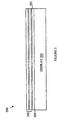
- FIG. 1 is a cross-sectional view of a portion of an OLED display 100 according to the present invention based on the color conversion methodology.
- Display 100 is constructed on a plastic substrate 161 such as the PET substrate material discussed above.
- the light that is converted to the primary colors is generated in an EL layer 118.
- the light in EL layer 118 is generated by connecting row and column electrodes to the appropriate power supplies.
- the row electrodes 117 will be assumed to be the anode of the device, and the column electrodes will be assumed to be the cathode.
- the cross-sectional view shown in Figure 1 is taken through one row electrode.
- the column electrodes run at right angles to the row electrodes.
- Typical column electrodes are shown at 131-133. Light generated at the intersection of a row and column electrode illuminates a color conversion strip that lies below the column electrode.
- the color conversion strips corresponding to electrodes 131-133 are shown at 121-123, respectively.
- Strip 121 converts the light emitted by layer 118 to blue light.
- strip 122 converts the emitted light to green
- strip 123 converts the emitted light to red.
- the portion of the display shown in Figure 1 includes the column electrodes for three full color pixels shown at 113-115.
- the various organic layers that make up the light emitting and injection layers are deposited over the patterned anode electrodes. To simplify the drawing, these layers are shown as a single light emitting layer 118; however, it is to be understood that layer 118 may be constructed of a number of sub-layers that facilitate the injection of holes and electrons into an EL layer as described above. Since the fabrication of such a multilayer structure is conventional in the art, it will not be discussed in detail here. It is sufficient to note that the layers can be deposited by spin casting, dye sublimation, web coating, or various "printing" techniques depending on the particular material system chosen.
- the cathode lines are constructed from a low work-function material such as calcium or magnesium. Shadow masking techniques for depositing such electrodes are also well known in the art, and hence, will not be discussed in detail here.
- the final displays need to be encapsulated to prevent oxygen and moisture from penetrating to the cathode electrodes and the light emitting layers.
- Such encapsulation layers are shown at 171 and 172 in Figure 1.
- the encapsulating layers are constructed as PML layers analogous to those described above.
- Each encapsulation layer includes two polymer layers and a layer of inorganic oxide or nitride sandwiched therebetween.
- the polymer layers corresponding to encapsulation layer 171 are shown at 181 and 183, respectively.
- the oxide or nitride layer corresponding to encapsulation layer 171 is shown at 182.
- the polymer and oxide or nitride layers corresponding to encapsulation layer 172 are shown at 191, 193, and 192, respectively.
- the polymer layers are deposited by evaporating a monomer for the polymer into a coating chamber, which is typically evacuated.
- the portion of the device that is to be coated is niaintained at a temperature below the boiling point of the monomer by contacting that portion with a cold surface, typically a roller that the device is moving over during the coating process.
- the monomer solution condenses on the device forming a uniform liquid coat that fills in the various gaps thereby planarizing the surface.
- the monomers are then cross-linked by exposure to a radiation source such as a UV lamp.
- a radiation source such as a UV lamp.
- the inorganic oxide is applied over the polymerized polymer surface.
- the oxide was applied by sputtering or evaporation.
- the extremely smooth polymer surface provides a low defect surface for the application of the oxide. Accordingly, the oxide has relatively few pinholes through which oxygen or water can travel. However, the oxide layer still passes sufficient oxygen and/or water to limit the device lifetime.
- the present invention overcomes this limitation.
- the permeability of the oxide layer is determined both by the density of pinholes in the layer and density of the oxide material.
- the PML technology addresses the pinhole problem; however, the deposition techniques utilized in the prior art systems do not provide a sufficiently dense oxide layer to limit permeability to the desired levels.
- the present invention is based on the observation that oxide or nitride layers deposited by plasma enhanced chemical vapor deposition utilizing a high density plasma, electron cyclotron resonance source (ECR-PECVD) have significantly higher densities than those deposited by the methods taught in the prior art, while allowing deposition under conditions that do not damage the underlying polymer layers.
- ECR-PECVD electron cyclotron resonance source
- High-density plasmas are characterized as having a very small sheath voltage, on the order of 5 times the electron temperature in eV, at surfaces containing the plasma. This is in contrast with low density plasmas which have capacitive coupling and high sheath voltages at walls. In capacitive plasmas the power into the plasma is coupled to the potential of ions striking the walls. In high-density plasmas, the potential of ions striking the walls is inherently very low and can be controlled by adding capacitively coupled power at the substrate. Hence, a high-density plasma provides a high flux of low energy ions along with a high flux of reactive species that are generated at the surface to be coated. This enables the deposition of usable dielectrics at temperatures compatible with polymers. Dielectrics such as silicon nitride, silicon dioxide, aluminum oxide, silicon carbide, silicon oxynitride, and such can be deposited utilizing this technique.
- a number of high-density plasma systems are available.
- such systems may be purchased from PlasmaQuest, Plasma-Therm, Surface Technology Systems, Trikon, Lam Research, Applied Materials, Tegal and Novellus.
- ECR is not necessary to create a high-density plasma and other schemes have been commercialized such as Inductively Coupled Plasma, Helical Resonator, and Helicon plasma.
- Inductively Coupled Plasma Helical Resonator
- Helicon plasma As an example for illustration only, we have found that an Oxford Instruments ECR system, using silane, argon and nitrogen as source gases at a pressure between 0.66 - 1.33 Pa (5 and 10 mTorr), with 700 Watts of 2.45 GHz microwave power and a magnetic field of about 875 Gauss, gave excellent results as described below. These operating parameters may be varied considerably as will be evident to those skilled in the art, to optimize conditions for particular substrates.
- a silicon nitride film was deposited by this technique on a thin calcium film (about 200 angstroms, prepared by thermal evaporation of calcium) on glass.
- the temperature of the film was maintained below 80°C by a cooling stage.
- the metal adjacent to pinholes became transparent, and the transparent diameter grew slowly larger with time.
- the remaining metal was unchanged in appearance in the microscope after 20 days. Given that a reaction of even 1% of the calcium would be visible (because of the surface disturbance), this observation gives an upper limit to the permeation rate of about 8 x 10 -7 moles H 2 O/m 2 day.
- etch rate of the film in a 10% (by volume) aqueous HF solution which is a good measure of its morphological quality, was 120 nm/min, which by comparison with published data (Y. Tessier, et al., Mat. Res. Soc. Symp. Proc. Vol. 86, 1986, p. 183) is indicative of a water permeability of around 1 x 10 -8 mol/m 2 day, 40 times better than the requirement for organic LEDs.
- a further important advantage of the present invention is that the stress of the deposited inorganic film can be varied, depending on the parameters such as the microwave power and gas pressure.
- the reduced stress reduces the distortions of the patterned elements and prevents delamination or distortion as the substrate is rolled up during roll-to-roll processing.
- the example film had a stress of 2.5 x 10 -9 dynes/cm 2 , which is quite low.
- a further advantage of the present invention is an improved deposition rate over the prior art methods discussed above. With the method of the present invention, rates of more than 1 micron per minute can be achieved. Since the deposition rate determines the maximum rate at which the roll-to-roll processing equipment can operate, the present invention provides increased throughput.
- the polymer layers are constructed from an acrylic monomer, such as methyl methacrylate, ethylene glycol diacrylate, or other acrylates, diacrylates, and triacrylates or methacrylates having a thickness of about 1 micron.
- the oxide layer is preferably silicon nitride having a thickness of 350 ⁇ .
- layers 182 and 192 can be constructed from silicon or aluminum oxides or aluminum nitride.
- the second polymer layer is used to protect the nitride layer from subsequent damage during use and processing.
- This layer is also preferably constructed from an acrylic monomer having a thickness of 0.25 microns or greater.
- other monomers such as carbonates, fluorinated alkenes, or other liquid monomers that can be cured to an insoluble film, can be utilized
- embodiments of the present invention utilize an encapsulation layer that is on the opposite side of the substrate film from the anode electrodes
- embodiments in which the substrate is coated with a PML film and the anode applied to the polymer layer may also be constructed.
- the smooth surface provided by the polymer layer is superior to that provided by a PET substrate.
- the resultant anode electrodes have fewer defects than those obtained by application of the ITO layer directly to the PET.
- the PET coated substrate can be prepared separately and stored, thereby relieving the manufacturer of the OLED device of the need to perform the first encapsulation operation.
- the barrier system of the present invention may be further enhanced by including a layer that absorbs oxygen and/or water.
- a “getter” layer can be constructed by providing a layer of material that reacts with oxygen or water that penetrates the layer and thereby removes the oxygen or water before it reaches the display device.
- a small amount of a getter compound is included in the oxide or nitride layer itself.
- a low concentration of metallic lithium can be added to an oxide or nitride layer that is formed by co-evaporation or co-sputtering from two sources.
- the concentration must be sufficiently low to maintain the transparency of the barrier if the layer is on the light emitting side of the device.
- the lithium will react with oxygen and/or water until the metallic lithium is expended, and the permeability of the layer will be lower than it was initially, because the free volume is now occupied by the chemically bound oxygen atoms. Hence, the device will be further protected for some period of time from oxygen or water that would have otherwise penetrated the barrier.
- the getter layer can be placed between the barrier and the device as a separate layer as shown in Figure 2 at 200.
- a separate layer of getter material 201 is placed between the PML barrier layer 202 and the device 203.
- An additional polymer layer 204 may be utilized to separate the getter layer from the device.
- a similar structure is provided on the other side of the device to prevent oxygen and/or water from penetrating from that side as well.
- the PML smoothing layer improves the quality of the getter layer compared to those described in the prior art, for example in the US #5,047,687 and 5,059,861.
- the getter material may be any metal that reacts rapidly with water, such as calcium, magnesium, or any alkali metal. Because the metals are protected by the PML-based water/oxygen barrier, highly reactive metals that are otherwise hard to handle may be used.
- the barrier system of the present invention has been described in terms of preventing water or oxygen from reaching the active layers of an OLED. However, it will be obvious to those skilled in the art from the preceding discussion that the method of the present invention may be used to provide an oxygen or water barrier for other types of devices or films.
Landscapes
- Physics & Mathematics (AREA)
- Optics & Photonics (AREA)
- Chemical & Material Sciences (AREA)
- Inorganic Chemistry (AREA)
- Electroluminescent Light Sources (AREA)
Applications Claiming Priority (2)
| Application Number | Priority Date | Filing Date | Title |
|---|---|---|---|
| US09/126,689 US6146225A (en) | 1998-07-30 | 1998-07-30 | Transparent, flexible permeability barrier for organic electroluminescent devices |
| US126689 | 1998-07-30 |
Publications (3)
| Publication Number | Publication Date |
|---|---|
| EP0977469A2 EP0977469A2 (en) | 2000-02-02 |
| EP0977469A3 EP0977469A3 (en) | 2000-09-20 |
| EP0977469B1 true EP0977469B1 (en) | 2003-09-24 |
Family
ID=22426201
Family Applications (1)
| Application Number | Title | Priority Date | Filing Date |
|---|---|---|---|
| EP99114946A Expired - Lifetime EP0977469B1 (en) | 1998-07-30 | 1999-07-30 | Improved transparent, flexible permeability barrier for organic electroluminescent devices |
Country Status (4)
| Country | Link |
|---|---|
| US (1) | US6146225A (enExample) |
| EP (1) | EP0977469B1 (enExample) |
| JP (1) | JP4985898B2 (enExample) |
| DE (1) | DE69911524T2 (enExample) |
Cited By (9)
| Publication number | Priority date | Publication date | Assignee | Title |
|---|---|---|---|---|
| US6866901B2 (en) | 1999-10-25 | 2005-03-15 | Vitex Systems, Inc. | Method for edge sealing barrier films |
| US6962671B2 (en) | 1999-10-25 | 2005-11-08 | Battelle Memorial Institute | Multilayer plastic substrates |
| US7198832B2 (en) | 1999-10-25 | 2007-04-03 | Vitex Systems, Inc. | Method for edge sealing barrier films |
| US7722929B2 (en) | 2005-08-18 | 2010-05-25 | Corning Incorporated | Sealing technique for decreasing the time it takes to hermetically seal a device and the resulting hermetically sealed device |
| US7829147B2 (en) | 2005-08-18 | 2010-11-09 | Corning Incorporated | Hermetically sealing a device without a heat treating step and the resulting hermetically sealed device |
| US8034452B2 (en) | 2005-07-20 | 2011-10-11 | 3M Innovative Properties Company | Moisture barrier coatings |
| US8241752B2 (en) | 1998-11-02 | 2012-08-14 | 3M Innovative Properties Company | Transparent conductive articles and methods of making same |
| US8350451B2 (en) | 2008-06-05 | 2013-01-08 | 3M Innovative Properties Company | Ultrathin transparent EMI shielding film comprising a polymer basecoat and crosslinked polymer transparent dielectric layer |
| US9050622B2 (en) | 2005-08-18 | 2015-06-09 | Corning Incorporated | Method for inhibiting oxygen and moisture degradation of a device and the resulting device |
Families Citing this family (217)
| Publication number | Priority date | Publication date | Assignee | Title |
|---|---|---|---|---|
| US6224948B1 (en) | 1997-09-29 | 2001-05-01 | Battelle Memorial Institute | Plasma enhanced chemical deposition with low vapor pressure compounds |
| US7126161B2 (en) | 1998-10-13 | 2006-10-24 | Semiconductor Energy Laboratory Co., Ltd. | Semiconductor device having El layer and sealing material |
| US6274887B1 (en) | 1998-11-02 | 2001-08-14 | Semiconductor Energy Laboratory Co., Ltd. | Semiconductor device and manufacturing method therefor |
| US7141821B1 (en) * | 1998-11-10 | 2006-11-28 | Semiconductor Energy Laboratory Co., Ltd. | Semiconductor device having an impurity gradient in the impurity regions and method of manufacture |
| US7022556B1 (en) * | 1998-11-11 | 2006-04-04 | Semiconductor Energy Laboratory Co., Ltd. | Exposure device, exposure method and method of manufacturing semiconductor device |
| US6277679B1 (en) | 1998-11-25 | 2001-08-21 | Semiconductor Energy Laboratory Co., Ltd. | Method of manufacturing thin film transistor |
| JP3912711B2 (ja) * | 1998-11-27 | 2007-05-09 | ローム株式会社 | 有機el素子 |
| US6207238B1 (en) * | 1998-12-16 | 2001-03-27 | Battelle Memorial Institute | Plasma enhanced chemical deposition for high and/or low index of refraction polymers |
| US6228436B1 (en) | 1998-12-16 | 2001-05-08 | Battelle Memorial Institute | Method of making light emitting polymer composite material |
| US6274204B1 (en) | 1998-12-16 | 2001-08-14 | Battelle Memorial Institute | Method of making non-linear optical polymer |
| US6217947B1 (en) | 1998-12-16 | 2001-04-17 | Battelle Memorial Institute | Plasma enhanced polymer deposition onto fixtures |
| US6228434B1 (en) | 1998-12-16 | 2001-05-08 | Battelle Memorial Institute | Method of making a conformal coating of a microtextured surface |
| US6268695B1 (en) | 1998-12-16 | 2001-07-31 | Battelle Memorial Institute | Environmental barrier material for organic light emitting device and method of making |
| US6207239B1 (en) | 1998-12-16 | 2001-03-27 | Battelle Memorial Institute | Plasma enhanced chemical deposition of conjugated polymer |
| EP1145338B1 (en) * | 1998-12-16 | 2012-12-05 | Samsung Display Co., Ltd. | Environmental barrier material for organic light emitting device and method of making |
| US7697052B1 (en) | 1999-02-17 | 2010-04-13 | Semiconductor Energy Laboratory Co., Ltd. | Electronic view finder utilizing an organic electroluminescence display |
| US6358570B1 (en) | 1999-03-31 | 2002-03-19 | Battelle Memorial Institute | Vacuum deposition and curing of oligomers and resins |
| US6506461B2 (en) | 1999-03-31 | 2003-01-14 | Battelle Memorial Institute | Methods for making polyurethanes as thin films |
| US6680487B1 (en) | 1999-05-14 | 2004-01-20 | Semiconductor Energy Laboratory Co., Ltd. | Semiconductor comprising a TFT provided on a substrate having an insulating surface and method of fabricating the same |
| US8853696B1 (en) | 1999-06-04 | 2014-10-07 | Semiconductor Energy Laboratory Co., Ltd. | Electro-optical device and electronic device |
| TWI232595B (en) | 1999-06-04 | 2005-05-11 | Semiconductor Energy Lab | Electroluminescence display device and electronic device |
| US7288420B1 (en) | 1999-06-04 | 2007-10-30 | Semiconductor Energy Laboratory Co., Ltd. | Method for manufacturing an electro-optical device |
| US6174613B1 (en) * | 1999-07-29 | 2001-01-16 | Agilent Technologies, Inc. | Method and apparatus for fabricating polymer-based electroluminescent displays |
| US6660409B1 (en) * | 1999-09-16 | 2003-12-09 | Panasonic Communications Co., Ltd | Electronic device and process for producing the same |
| TW522453B (en) | 1999-09-17 | 2003-03-01 | Semiconductor Energy Lab | Display device |
| JP3942770B2 (ja) * | 1999-09-22 | 2007-07-11 | 株式会社半導体エネルギー研究所 | El表示装置及び電子装置 |
| TW480722B (en) | 1999-10-12 | 2002-03-21 | Semiconductor Energy Lab | Manufacturing method of electro-optical device |
| US20100330748A1 (en) | 1999-10-25 | 2010-12-30 | Xi Chu | Method of encapsulating an environmentally sensitive device |
| US6413645B1 (en) * | 2000-04-20 | 2002-07-02 | Battelle Memorial Institute | Ultrabarrier substrates |
| US6548912B1 (en) | 1999-10-25 | 2003-04-15 | Battelle Memorial Institute | Semicoductor passivation using barrier coatings |
| US6573652B1 (en) | 1999-10-25 | 2003-06-03 | Battelle Memorial Institute | Encapsulated display devices |
| KR100720066B1 (ko) | 1999-11-09 | 2007-05-18 | 가부시키가이샤 한도오따이 에네루기 켄큐쇼 | 발광장치 제작방법 |
| US6646287B1 (en) | 1999-11-19 | 2003-11-11 | Semiconductor Energy Laboratory Co., Ltd. | Semiconductor device with tapered gate and insulating film |
| US20010053559A1 (en) * | 2000-01-25 | 2001-12-20 | Semiconductor Energy Laboratory Co., Ltd. | Method of fabricating display device |
| US6492026B1 (en) * | 2000-04-20 | 2002-12-10 | Battelle Memorial Institute | Smoothing and barrier layers on high Tg substrates |
| US6465953B1 (en) * | 2000-06-12 | 2002-10-15 | General Electric Company | Plastic substrates with improved barrier properties for devices sensitive to water and/or oxygen, such as organic electroluminescent devices |
| US6867539B1 (en) | 2000-07-12 | 2005-03-15 | 3M Innovative Properties Company | Encapsulated organic electronic devices and method for making same |
| US6605826B2 (en) * | 2000-08-18 | 2003-08-12 | Semiconductor Energy Laboratory Co., Ltd. | Light-emitting device and display device |
| US6924594B2 (en) * | 2000-10-03 | 2005-08-02 | Semiconductor Energy Laboratory Co., Ltd. | Light emitting device |
| JP4618862B2 (ja) * | 2000-10-30 | 2011-01-26 | 大日本印刷株式会社 | バリア性積層構造体を用いて封止された封止el素子 |
| US7199527B2 (en) * | 2000-11-21 | 2007-04-03 | Alien Technology Corporation | Display device and methods of manufacturing and control |
| US6537688B2 (en) | 2000-12-01 | 2003-03-25 | Universal Display Corporation | Adhesive sealed organic optoelectronic structures |
| JP2002175881A (ja) * | 2000-12-07 | 2002-06-21 | Fuji Photo Film Co Ltd | 発光素子 |
| US6614057B2 (en) | 2001-02-07 | 2003-09-02 | Universal Display Corporation | Sealed organic optoelectronic structures |
| US7222981B2 (en) * | 2001-02-15 | 2007-05-29 | Semiconductor Energy Laboratory Co., Ltd. | EL display device and electronic device |
| US6576351B2 (en) | 2001-02-16 | 2003-06-10 | Universal Display Corporation | Barrier region for optoelectronic devices |
| US6822391B2 (en) * | 2001-02-21 | 2004-11-23 | Semiconductor Energy Laboratory Co., Ltd. | Light emitting device, electronic equipment, and method of manufacturing thereof |
| US6624568B2 (en) | 2001-03-28 | 2003-09-23 | Universal Display Corporation | Multilayer barrier region containing moisture- and oxygen-absorbing material for optoelectronic devices |
| US6664137B2 (en) | 2001-03-29 | 2003-12-16 | Universal Display Corporation | Methods and structures for reducing lateral diffusion through cooperative barrier layers |
| JP2002359071A (ja) * | 2001-04-20 | 2002-12-13 | Lg Phillips Lcd Co Ltd | 有機発光素子 |
| KR100415615B1 (ko) | 2001-06-13 | 2004-01-24 | 엘지전자 주식회사 | 게터 조성물 및 이를 이용한 전계방출표시소자 |
| US6692326B2 (en) | 2001-06-16 | 2004-02-17 | Cld, Inc. | Method of making organic electroluminescent display |
| US7294517B2 (en) | 2001-06-18 | 2007-11-13 | Semiconductor Energy Laboratory Co., Ltd. | Light emitting device and method of fabricating the same |
| US7211828B2 (en) * | 2001-06-20 | 2007-05-01 | Semiconductor Energy Laboratory Co., Ltd. | Light emitting device and electronic apparatus |
| TW548860B (en) * | 2001-06-20 | 2003-08-21 | Semiconductor Energy Lab | Light emitting device and method of manufacturing the same |
| JP2003086356A (ja) * | 2001-09-06 | 2003-03-20 | Semiconductor Energy Lab Co Ltd | 発光装置及び電子機器 |
| TW546857B (en) * | 2001-07-03 | 2003-08-11 | Semiconductor Energy Lab | Light-emitting device, method of manufacturing a light-emitting device, and electronic equipment |
| US7469558B2 (en) | 2001-07-10 | 2008-12-30 | Springworks, Llc | As-deposited planar optical waveguides with low scattering loss and methods for their manufacture |
| TW564471B (en) | 2001-07-16 | 2003-12-01 | Semiconductor Energy Lab | Semiconductor device and peeling off method and method of manufacturing semiconductor device |
| KR100413450B1 (ko) | 2001-07-20 | 2003-12-31 | 엘지전자 주식회사 | 표시소자의 보호막 구조 |
| CN1317421C (zh) * | 2001-08-20 | 2007-05-23 | 诺华等离子公司 | 气体和蒸气低渗透性的涂层 |
| US6888307B2 (en) * | 2001-08-21 | 2005-05-03 | Universal Display Corporation | Patterned oxygen and moisture absorber for organic optoelectronic device structures |
| TW558743B (en) | 2001-08-22 | 2003-10-21 | Semiconductor Energy Lab | Peeling method and method of manufacturing semiconductor device |
| JP4166455B2 (ja) * | 2001-10-01 | 2008-10-15 | 株式会社半導体エネルギー研究所 | 偏光フィルム及び発光装置 |
| US6888305B2 (en) * | 2001-11-06 | 2005-05-03 | Universal Display Corporation | Encapsulation structure that acts as a multilayer mirror |
| US7404877B2 (en) | 2001-11-09 | 2008-07-29 | Springworks, Llc | Low temperature zirconia based thermal barrier layer by PVD |
| US6730373B2 (en) * | 2001-11-21 | 2004-05-04 | Optical Coating Laboratory, Inc. | Glass panel with barrier coating and related methods |
| US6597111B2 (en) | 2001-11-27 | 2003-07-22 | Universal Display Corporation | Protected organic optoelectronic devices |
| US7050835B2 (en) * | 2001-12-12 | 2006-05-23 | Universal Display Corporation | Intelligent multi-media display communication system |
| US7265807B2 (en) * | 2001-12-13 | 2007-09-04 | Koninklijke Philips Electronics N.V. | Sealing structure for display devices |
| US6765351B2 (en) * | 2001-12-20 | 2004-07-20 | The Trustees Of Princeton University | Organic optoelectronic device structures |
| US7012363B2 (en) * | 2002-01-10 | 2006-03-14 | Universal Display Corporation | OLEDs having increased external electroluminescence quantum efficiencies |
| US6884327B2 (en) | 2002-03-16 | 2005-04-26 | Tao Pan | Mode size converter for a planar waveguide |
| US7378356B2 (en) | 2002-03-16 | 2008-05-27 | Springworks, Llc | Biased pulse DC reactive sputtering of oxide films |
| US6891330B2 (en) * | 2002-03-29 | 2005-05-10 | General Electric Company | Mechanically flexible organic electroluminescent device with directional light emission |
| US6897474B2 (en) * | 2002-04-12 | 2005-05-24 | Universal Display Corporation | Protected organic electronic devices and methods for making the same |
| US6835950B2 (en) | 2002-04-12 | 2004-12-28 | Universal Display Corporation | Organic electronic devices with pressure sensitive adhesive layer |
| US8900366B2 (en) | 2002-04-15 | 2014-12-02 | Samsung Display Co., Ltd. | Apparatus for depositing a multilayer coating on discrete sheets |
| US8808457B2 (en) | 2002-04-15 | 2014-08-19 | Samsung Display Co., Ltd. | Apparatus for depositing a multilayer coating on discrete sheets |
| DE10222958B4 (de) * | 2002-04-15 | 2007-08-16 | Schott Ag | Verfahren zur Herstellung eines organischen elektro-optischen Elements und organisches elektro-optisches Element |
| US7268486B2 (en) | 2002-04-15 | 2007-09-11 | Schott Ag | Hermetic encapsulation of organic, electro-optical elements |
| KR100475849B1 (ko) * | 2002-04-17 | 2005-03-10 | 한국전자통신연구원 | 습식 공정에 의하여 형성된 엔캡슐레이션 박막을 갖춘유기 전기발광 소자 및 그 제조 방법 |
| KR100462469B1 (ko) * | 2002-04-17 | 2004-12-17 | 한국전자통신연구원 | 접착식 유기-무기 복합막을 갖춘 엔캡슐레이션 박막과이를 포함하는 유기 전기발광 소자 |
| EP1506693B1 (en) * | 2002-05-10 | 2006-09-27 | Koninklijke Philips Electronics N.V. | Electroluminescent panel |
| US7164155B2 (en) | 2002-05-15 | 2007-01-16 | Semiconductor Energy Laboratory Co., Ltd. | Light emitting device |
| US7230271B2 (en) | 2002-06-11 | 2007-06-12 | Semiconductor Energy Laboratory Co., Ltd. | Light emitting device comprising film having hygroscopic property and transparency and manufacturing method thereof |
| KR100819297B1 (ko) * | 2002-06-26 | 2008-04-02 | 삼성전자주식회사 | 고반사율 미세 패턴의 제조방법 |
| KR100484954B1 (ko) * | 2002-07-08 | 2005-04-22 | 엘지.필립스 엘시디 주식회사 | 유기 전계발광 소자의 엔캡슐레이션 방법 |
| US8236443B2 (en) | 2002-08-09 | 2012-08-07 | Infinite Power Solutions, Inc. | Metal film encapsulation |
| US20070264564A1 (en) | 2006-03-16 | 2007-11-15 | Infinite Power Solutions, Inc. | Thin film battery on an integrated circuit or circuit board and method thereof |
| US8404376B2 (en) | 2002-08-09 | 2013-03-26 | Infinite Power Solutions, Inc. | Metal film encapsulation |
| US8394522B2 (en) | 2002-08-09 | 2013-03-12 | Infinite Power Solutions, Inc. | Robust metal film encapsulation |
| US8431264B2 (en) | 2002-08-09 | 2013-04-30 | Infinite Power Solutions, Inc. | Hybrid thin-film battery |
| US8021778B2 (en) | 2002-08-09 | 2011-09-20 | Infinite Power Solutions, Inc. | Electrochemical apparatus with barrier layer protected substrate |
| US7993773B2 (en) | 2002-08-09 | 2011-08-09 | Infinite Power Solutions, Inc. | Electrochemical apparatus with barrier layer protected substrate |
| US8445130B2 (en) | 2002-08-09 | 2013-05-21 | Infinite Power Solutions, Inc. | Hybrid thin-film battery |
| US6933051B2 (en) * | 2002-08-17 | 2005-08-23 | 3M Innovative Properties Company | Flexible electrically conductive film |
| US6929864B2 (en) * | 2002-08-17 | 2005-08-16 | 3M Innovative Properties Company | Extensible, visible light-transmissive and infrared-reflective film and methods of making and using the film |
| US6818291B2 (en) * | 2002-08-17 | 2004-11-16 | 3M Innovative Properties Company | Durable transparent EMI shielding film |
| US7215473B2 (en) * | 2002-08-17 | 2007-05-08 | 3M Innovative Properties Company | Enhanced heat mirror films |
| AU2003261463A1 (en) | 2002-08-27 | 2004-03-19 | Symmorphix, Inc. | Optically coupling into highly uniform waveguides |
| US6994933B1 (en) | 2002-09-16 | 2006-02-07 | Oak Ridge Micro-Energy, Inc. | Long life thin film battery and method therefor |
| CN1176565C (zh) * | 2002-11-25 | 2004-11-17 | 清华大学 | 一种有机电致发光器件的封装层及其制备方法和应用 |
| US7710019B2 (en) | 2002-12-11 | 2010-05-04 | Samsung Electronics Co., Ltd. | Organic light-emitting diode display comprising auxiliary electrodes |
| AU2003287820A1 (en) * | 2002-12-20 | 2004-07-14 | Ifire Technology Corp. | Aluminum nitride passivated phosphors for electroluminescent displays |
| WO2004077519A2 (en) | 2003-02-27 | 2004-09-10 | Mukundan Narasimhan | Dielectric barrier layer films |
| US20060158101A1 (en) * | 2003-03-04 | 2006-07-20 | Dow Corning Corporation | Organic light-emitting diode |
| US20070184181A1 (en) * | 2003-03-25 | 2007-08-09 | Kazuo Wada | Device and method for forming film for organic electro-luminescence element using inductive coupling CVD |
| US7018713B2 (en) * | 2003-04-02 | 2006-03-28 | 3M Innovative Properties Company | Flexible high-temperature ultrabarrier |
| US7510913B2 (en) | 2003-04-11 | 2009-03-31 | Vitex Systems, Inc. | Method of making an encapsulated plasma sensitive device |
| US7648925B2 (en) | 2003-04-11 | 2010-01-19 | Vitex Systems, Inc. | Multilayer barrier stacks and methods of making multilayer barrier stacks |
| US20040206953A1 (en) * | 2003-04-16 | 2004-10-21 | Robert Morena | Hermetically sealed glass package and method of fabrication |
| US7344901B2 (en) * | 2003-04-16 | 2008-03-18 | Corning Incorporated | Hermetically sealed package and method of fabricating of a hermetically sealed package |
| US6998776B2 (en) * | 2003-04-16 | 2006-02-14 | Corning Incorporated | Glass package that is hermetically sealed with a frit and method of fabrication |
| US7238628B2 (en) | 2003-05-23 | 2007-07-03 | Symmorphix, Inc. | Energy conversion and storage films and devices by physical vapor deposition of titanium and titanium oxides and sub-oxides |
| US8728285B2 (en) | 2003-05-23 | 2014-05-20 | Demaray, Llc | Transparent conductive oxides |
| US20040238846A1 (en) * | 2003-05-30 | 2004-12-02 | Georg Wittmann | Organic electronic device |
| JP2007505445A (ja) * | 2003-07-07 | 2007-03-08 | アイファイアー・テクノロジー・コープ | エレクトロルミネセント・ディスプレイのためのシールおよびシール方法 |
| US6998648B2 (en) * | 2003-08-25 | 2006-02-14 | Universal Display Corporation | Protected organic electronic device structures incorporating pressure sensitive adhesive and desiccant |
| US8722160B2 (en) | 2003-10-31 | 2014-05-13 | Aeris Capital Sustainable Ip Ltd. | Inorganic/organic hybrid nanolaminate barrier film |
| US7495644B2 (en) * | 2003-12-26 | 2009-02-24 | Semiconductor Energy Laboratory Co., Ltd. | Display device and method for manufacturing display device |
| CN1328936C (zh) * | 2004-01-05 | 2007-07-25 | 统宝光电股份有限公司 | 形成封装保护结构的方法 |
| DE102004005370B4 (de) * | 2004-02-03 | 2007-08-16 | Samsung SDI Co., Ltd., Suwon | Elektrisches Gerät mit einem Gehäuse und einem OLED-Anzeigeelement sowie Verfahren zu dessen Herstellung |
| US7202504B2 (en) | 2004-05-20 | 2007-04-10 | Semiconductor Energy Laboratory Co., Ltd. | Light-emitting element and display device |
| DE102004026618A1 (de) * | 2004-06-01 | 2005-12-29 | Siemens Ag | Röntgendetektor |
| US20050269943A1 (en) * | 2004-06-04 | 2005-12-08 | Michael Hack | Protected organic electronic devices and methods for making the same |
| US7812522B2 (en) * | 2004-07-22 | 2010-10-12 | Ifire Ip Corporation | Aluminum oxide and aluminum oxynitride layers for use with phosphors for electroluminescent displays |
| US20090032108A1 (en) * | 2007-03-30 | 2009-02-05 | Craig Leidholm | Formation of photovoltaic absorber layers on foil substrates |
| US20060063015A1 (en) * | 2004-09-23 | 2006-03-23 | 3M Innovative Properties Company | Protected polymeric film |
| US7342356B2 (en) * | 2004-09-23 | 2008-03-11 | 3M Innovative Properties Company | Organic electroluminescent device having protective structure with boron oxide layer and inorganic barrier layer |
| US20060093795A1 (en) * | 2004-11-04 | 2006-05-04 | Eastman Kodak Company | Polymeric substrate having a desiccant layer |
| KR101127370B1 (ko) | 2004-12-08 | 2012-03-29 | 인피니트 파워 솔루션스, 인크. | LiCoO2의 증착 |
| US7959769B2 (en) | 2004-12-08 | 2011-06-14 | Infinite Power Solutions, Inc. | Deposition of LiCoO2 |
| US20060153997A1 (en) * | 2005-01-07 | 2006-07-13 | Eastman Kodak Company | Method of varying wavelengths of liquid crystals |
| TW200700144A (en) * | 2005-01-14 | 2007-01-01 | Matsushita Electric Industrial Co Ltd | Gas-absorbing substance, gas-absorbing alloy and gas-absorbing material |
| KR100623731B1 (ko) * | 2005-03-16 | 2006-09-14 | 삼성에스디아이 주식회사 | 유기전계발광표시장치 및 그의 제조 방법 |
| ITMI20051502A1 (it) * | 2005-07-29 | 2007-01-30 | Getters Spa | Sistemi getter comprendenti uno o piu' depositi di materiale getter ed uno strato di materiale per il trasporto di h02o |
| US7767498B2 (en) | 2005-08-25 | 2010-08-03 | Vitex Systems, Inc. | Encapsulated devices and method of making |
| US7838133B2 (en) | 2005-09-02 | 2010-11-23 | Springworks, Llc | Deposition of perovskite and other compound ceramic films for dielectric applications |
| US8193705B2 (en) * | 2005-11-02 | 2012-06-05 | Ifire Ip Corporation | Laminated conformal seal for electroluminescent displays |
| US7537504B2 (en) * | 2005-12-06 | 2009-05-26 | Corning Incorporated | Method of encapsulating a display element with frit wall and laser beam |
| US7597603B2 (en) * | 2005-12-06 | 2009-10-06 | Corning Incorporated | Method of encapsulating a display element |
| US20070131944A1 (en) * | 2005-12-08 | 2007-06-14 | Au Optronics Corporation | Dual organic electroluminescent display and method of making same |
| JP4539547B2 (ja) * | 2005-12-08 | 2010-09-08 | セイコーエプソン株式会社 | 発光装置、発光装置の製造方法、及び電子機器 |
| US8044571B2 (en) * | 2005-12-14 | 2011-10-25 | General Electric Company | Electrode stacks for electroactive devices and methods of fabricating the same |
| US8158450B1 (en) * | 2006-05-05 | 2012-04-17 | Nanosolar, Inc. | Barrier films and high throughput manufacturing processes for photovoltaic devices |
| US20080006819A1 (en) * | 2006-06-19 | 2008-01-10 | 3M Innovative Properties Company | Moisture barrier coatings for organic light emitting diode devices |
| US20080124558A1 (en) * | 2006-08-18 | 2008-05-29 | Heather Debra Boek | Boro-silicate glass frits for hermetic sealing of light emitting device displays |
| US20080048178A1 (en) | 2006-08-24 | 2008-02-28 | Bruce Gardiner Aitken | Tin phosphate barrier film, method, and apparatus |
| KR20090069323A (ko) | 2006-09-29 | 2009-06-30 | 인피니트 파워 솔루션스, 인크. | 가요성 기판의 마스킹 및 가요성 기판에 배터리 층을 증착하기 위한 재료의 구속 |
| DE102006048339A1 (de) * | 2006-10-12 | 2008-04-24 | Agfaphoto Gmbh | Schutzfolie |
| US20080100202A1 (en) * | 2006-11-01 | 2008-05-01 | Cok Ronald S | Process for forming oled conductive protective layer |
| US8197781B2 (en) | 2006-11-07 | 2012-06-12 | Infinite Power Solutions, Inc. | Sputtering target of Li3PO4 and method for producing same |
| US8115326B2 (en) | 2006-11-30 | 2012-02-14 | Corning Incorporated | Flexible substrates having a thin-film barrier |
| EP2125361B1 (en) | 2006-12-28 | 2019-01-23 | 3M Innovative Properties Company | Nucleation layer for thin film metal layer formation |
| JP5249240B2 (ja) * | 2006-12-29 | 2013-07-31 | スリーエム イノベイティブ プロパティズ カンパニー | 金属アルコキシド含有フィルムの硬化方法 |
| KR20170019491A (ko) * | 2006-12-29 | 2017-02-21 | 쓰리엠 이노베이티브 프로퍼티즈 컴파니 | 무기 또는 무기/유기 하이브리드 필름의 제조 방법 |
| NL1033860C2 (nl) | 2007-05-16 | 2008-11-18 | Otb Group Bv | Werkwijze voor het aanbrengen van een dunnefilm-encapsulatielaagsamenstel op een organisch device en een organisch device voorzien van een dunnefilm-encapsulatielaagsamenstel bij voorkeur aangebracht met een dergelijke werkwijze. |
| JP5208591B2 (ja) | 2007-06-28 | 2013-06-12 | 株式会社半導体エネルギー研究所 | 発光装置、及び照明装置 |
| CL2008002636A1 (es) | 2007-09-07 | 2009-06-19 | Avery Dennison Corp | Un rótulo para cubrir identificación existente en sustratos como paquetes o envases de tal manera que el sustrato puede ser reutilizado, hoja de rótulos y método de fabricación. |
| WO2009053886A2 (en) * | 2007-10-25 | 2009-04-30 | Koninklijke Philips Electronics N.V. | Organic electro-optical device, light source, display device and solar cell |
| US20090162667A1 (en) * | 2007-12-20 | 2009-06-25 | Lumination Llc | Lighting device having backlighting, illumination and display applications |
| US8268488B2 (en) | 2007-12-21 | 2012-09-18 | Infinite Power Solutions, Inc. | Thin film electrolyte for thin film batteries |
| WO2009086038A1 (en) | 2007-12-21 | 2009-07-09 | Infinite Power Solutions, Inc. | Method for sputter targets for electrolyte films |
| KR100832847B1 (ko) * | 2007-12-21 | 2008-05-28 | (주)누리셀 | 평탄화 유기 박막 및 컨포멀 유기 박막을 포함하는 다층봉지막 |
| CN101945965A (zh) | 2007-12-28 | 2011-01-12 | 3M创新有限公司 | 柔性封装膜系统 |
| CN101911367B (zh) | 2008-01-11 | 2015-02-25 | 无穷动力解决方案股份有限公司 | 用于薄膜电池及其他器件的薄膜包封 |
| KR101672254B1 (ko) | 2008-04-02 | 2016-11-08 | 사푸라스트 리써치 엘엘씨 | 에너지 수확과 관련된 에너지 저장 장치를 위한 수동적인 과전압/부족전압 제어 및 보호 |
| US8053984B2 (en) * | 2008-05-26 | 2011-11-08 | Lg Display Co., Ltd. | Organic light emitting diode display |
| US8448468B2 (en) | 2008-06-11 | 2013-05-28 | Corning Incorporated | Mask and method for sealing a glass envelope |
| US9481927B2 (en) * | 2008-06-30 | 2016-11-01 | 3M Innovative Properties Company | Method of making inorganic or inorganic/organic hybrid barrier films |
| US8906523B2 (en) | 2008-08-11 | 2014-12-09 | Infinite Power Solutions, Inc. | Energy device with integral collector surface for electromagnetic energy harvesting and method thereof |
| WO2010030743A1 (en) | 2008-09-12 | 2010-03-18 | Infinite Power Solutions, Inc. | Energy device with integral conductive surface for data communication via electromagnetic energy and method thereof |
| US8508193B2 (en) | 2008-10-08 | 2013-08-13 | Infinite Power Solutions, Inc. | Environmentally-powered wireless sensor module |
| JP2011003522A (ja) | 2008-10-16 | 2011-01-06 | Semiconductor Energy Lab Co Ltd | フレキシブル発光装置、電子機器及びフレキシブル発光装置の作製方法 |
| US20100095705A1 (en) | 2008-10-20 | 2010-04-22 | Burkhalter Robert S | Method for forming a dry glass-based frit |
| US9184410B2 (en) | 2008-12-22 | 2015-11-10 | Samsung Display Co., Ltd. | Encapsulated white OLEDs having enhanced optical output |
| US9337446B2 (en) | 2008-12-22 | 2016-05-10 | Samsung Display Co., Ltd. | Encapsulated RGB OLEDs having enhanced optical output |
| US8219408B2 (en) * | 2008-12-29 | 2012-07-10 | Motorola Mobility, Inc. | Audio signal decoder and method for producing a scaled reconstructed audio signal |
| US8680678B2 (en) * | 2009-06-01 | 2014-03-25 | Sumitomo Chemical Co., Ltd. | Formulations for improved electrodes for electronic devices |
| US8766269B2 (en) | 2009-07-02 | 2014-07-01 | Semiconductor Energy Laboratory Co., Ltd. | Light-emitting device, lighting device, and electronic device |
| US8599572B2 (en) | 2009-09-01 | 2013-12-03 | Infinite Power Solutions, Inc. | Printed circuit board with integrated thin film battery |
| US8580332B2 (en) * | 2009-09-22 | 2013-11-12 | Applied Materials, Inc. | Thin-film battery methods for complexity reduction |
| US9472783B2 (en) * | 2009-10-12 | 2016-10-18 | General Electric Company | Barrier coating with reduced process time |
| CN101707237B (zh) * | 2009-10-30 | 2011-08-17 | 彩虹集团公司 | 一种柔性有机电致发光器件的封装结构及其封装方法 |
| US8590338B2 (en) | 2009-12-31 | 2013-11-26 | Samsung Mobile Display Co., Ltd. | Evaporator with internal restriction |
| KR101155904B1 (ko) | 2010-01-04 | 2012-06-20 | 삼성모바일디스플레이주식회사 | 유기 발광 표시 장치 |
| US9000442B2 (en) * | 2010-01-20 | 2015-04-07 | Semiconductor Energy Laboratory Co., Ltd. | Light-emitting device, flexible light-emitting device, electronic device, and method for manufacturing light-emitting device and flexible-light emitting device |
| TWI589042B (zh) * | 2010-01-20 | 2017-06-21 | 半導體能源研究所股份有限公司 | 發光裝置,撓性發光裝置,電子裝置,照明設備,以及發光裝置和撓性發光裝置的製造方法 |
| EP2577777B1 (en) | 2010-06-07 | 2016-12-28 | Sapurast Research LLC | Rechargeable, high-density electrochemical device |
| TWI641287B (zh) | 2010-09-14 | 2018-11-11 | 半導體能源研究所股份有限公司 | 固態發光元件,發光裝置和照明裝置 |
| JP5827104B2 (ja) | 2010-11-19 | 2015-12-02 | 株式会社半導体エネルギー研究所 | 照明装置 |
| JP6118020B2 (ja) | 2010-12-16 | 2017-04-19 | 株式会社半導体エネルギー研究所 | 発光装置 |
| US8735874B2 (en) | 2011-02-14 | 2014-05-27 | Semiconductor Energy Laboratory Co., Ltd. | Light-emitting device, display device, and method for manufacturing the same |
| KR101922603B1 (ko) | 2011-03-04 | 2018-11-27 | 가부시키가이샤 한도오따이 에네루기 켄큐쇼 | 발광 장치, 조명 장치, 기판, 기판의 제작 방법 |
| KR101308480B1 (ko) * | 2011-06-14 | 2013-09-16 | 엘지디스플레이 주식회사 | 플라스틱 유기 전계 발광 표시 장치 및 그 제조 방법 |
| JP5504221B2 (ja) * | 2011-08-05 | 2014-05-28 | 株式会社半導体エネルギー研究所 | 発光装置及びその作製方法 |
| KR102079188B1 (ko) | 2012-05-09 | 2020-02-19 | 가부시키가이샤 한도오따이 에네루기 켄큐쇼 | 발광 장치 및 전자 기기 |
| KR101951223B1 (ko) | 2012-10-26 | 2019-02-25 | 삼성디스플레이 주식회사 | 표시장치 및 그 제조방법 |
| KR102309244B1 (ko) | 2013-02-20 | 2021-10-05 | 가부시키가이샤 한도오따이 에네루기 켄큐쇼 | 반도체 장치 |
| JP6477462B2 (ja) | 2013-03-27 | 2019-03-06 | 凸版印刷株式会社 | 積層体及びガスバリアフィルム |
| KR102084715B1 (ko) | 2013-06-18 | 2020-03-05 | 삼성디스플레이 주식회사 | 유기 발광 표시 장치 |
| CN105793957B (zh) | 2013-12-12 | 2019-05-03 | 株式会社半导体能源研究所 | 剥离方法及剥离装置 |
| CN104746036B (zh) * | 2013-12-31 | 2017-11-07 | 中国科学院微电子研究所 | 一种薄膜封装方法 |
| US9909022B2 (en) | 2014-07-25 | 2018-03-06 | Kateeva, Inc. | Organic thin film ink compositions and methods |
| US9923176B2 (en) | 2015-04-08 | 2018-03-20 | Stmicroelectronics (Tours) Sas | Power unit using flexible conductive member |
| CN105098090A (zh) * | 2015-06-15 | 2015-11-25 | 深圳市华星光电技术有限公司 | Oled器件的封装结构及其封装方法 |
| CN107922766A (zh) | 2015-08-31 | 2018-04-17 | 科迪华公司 | 基于二‑和单(甲基)丙烯酸酯的有机薄膜油墨组合物 |
| JP6457371B2 (ja) * | 2015-10-09 | 2019-01-23 | 富士フイルム株式会社 | ガスバリアフィルム、有機電子装置、有機電界発光装置用基板、有機電界発光装置 |
| TWI841527B (zh) | 2017-04-21 | 2024-05-11 | 美商凱特伊夫公司 | 用於形成有機薄膜的組成物和技術 |
| TWI742289B (zh) * | 2017-06-09 | 2021-10-11 | 南韓商Lg化學股份有限公司 | 封裝膜 |
| CN107369776B (zh) * | 2017-08-18 | 2020-05-08 | 京东方科技集团股份有限公司 | Oled器件的封装结构和oled器件 |
| CN109904345A (zh) * | 2019-02-28 | 2019-06-18 | 武汉华星光电半导体显示技术有限公司 | 封装结构及其显示装置 |
| US11588137B2 (en) | 2019-06-05 | 2023-02-21 | Semiconductor Energy Laboratory Co., Ltd. | Functional panel, display device, input/output device, and data processing device |
| US11659758B2 (en) | 2019-07-05 | 2023-05-23 | Semiconductor Energy Laboratory Co., Ltd. | Display unit, display module, and electronic device |
| KR20220031679A (ko) | 2019-07-12 | 2022-03-11 | 가부시키가이샤 한도오따이 에네루기 켄큐쇼 | 기능 패널, 표시 장치, 입출력 장치, 정보 처리 장치 |
| WO2021069999A1 (ja) | 2019-10-11 | 2021-04-15 | 株式会社半導体エネルギー研究所 | 機能パネル、表示装置、入出力装置、情報処理装置 |
Family Cites Families (22)
| Publication number | Priority date | Publication date | Assignee | Title |
|---|---|---|---|---|
| US4842893A (en) * | 1983-12-19 | 1989-06-27 | Spectrum Control, Inc. | High speed process for coating substrates |
| US4954371A (en) * | 1986-06-23 | 1990-09-04 | Spectrum Control, Inc. | Flash evaporation of monomer fluids |
| JPS6354295U (enExample) * | 1986-09-26 | 1988-04-12 | ||
| CA2004663A1 (en) * | 1988-12-05 | 1990-06-05 | Tsutomu Sawada | Moistureproof film |
| JP2820469B2 (ja) * | 1988-12-05 | 1998-11-05 | 三菱化学株式会社 | 防湿フィルム |
| KR0175919B1 (ko) * | 1990-10-17 | 1999-05-01 | 미우라 아끼라 | 내열성 방습 필름 |
| JP3020692B2 (ja) * | 1990-10-17 | 2000-03-15 | 三菱化学株式会社 | 耐熱性防湿フィルム |
| US5260095A (en) * | 1992-08-21 | 1993-11-09 | Battelle Memorial Institute | Vacuum deposition and curing of liquid monomers |
| JP3192249B2 (ja) * | 1992-10-27 | 2001-07-23 | 鐘淵化学工業株式会社 | ガス及び湿気バリアー膜及びその製造方法 |
| JP3277965B2 (ja) * | 1993-09-20 | 2002-04-22 | 東洋紡績株式会社 | エレクトロルミネッセンスパネル |
| JP3577117B2 (ja) * | 1994-10-07 | 2004-10-13 | Tdk株式会社 | 有機エレクトロルミネセンス素子の製法 |
| JP3261945B2 (ja) * | 1994-10-14 | 2002-03-04 | 東洋インキ製造株式会社 | エレクトロルミネッセンス素子封止用積層体およびエレクトロルミネッセンス素子封止構造体 |
| JPH0917572A (ja) * | 1995-06-26 | 1997-01-17 | Hewlett Packard Co <Hp> | 薄膜エレクトロルミネセンス素子のシール形成方法及びエレクトロルミネセンス素子 |
| JP3900543B2 (ja) * | 1995-07-17 | 2007-04-04 | 東洋紡績株式会社 | 積層フィルム |
| JP3539597B2 (ja) * | 1995-10-13 | 2004-07-07 | ソニー株式会社 | 有機光学的素子及びその製造方法 |
| US5686360A (en) * | 1995-11-30 | 1997-11-11 | Motorola | Passivation of organic devices |
| US5811177A (en) * | 1995-11-30 | 1998-09-22 | Motorola, Inc. | Passivation of electroluminescent organic devices |
| JPH09151371A (ja) * | 1995-11-30 | 1997-06-10 | Toppan Printing Co Ltd | 有機薄膜el素子 |
| JP2950240B2 (ja) * | 1996-06-24 | 1999-09-20 | 関西日本電気株式会社 | 電界発光灯 |
| JP3620186B2 (ja) * | 1996-12-12 | 2005-02-16 | 凸版印刷株式会社 | 有機薄膜el素子 |
| JPH10275680A (ja) * | 1997-03-31 | 1998-10-13 | Toyota Central Res & Dev Lab Inc | 有機el素子 |
| KR100580351B1 (ko) * | 1997-04-17 | 2006-05-16 | 가부시끼가이샤 구레하 | 방습 필름 및 전기 발광 소자 |
-
1998
- 1998-07-30 US US09/126,689 patent/US6146225A/en not_active Expired - Lifetime
-
1999
- 1999-07-29 JP JP21568499A patent/JP4985898B2/ja not_active Expired - Fee Related
- 1999-07-30 DE DE69911524T patent/DE69911524T2/de not_active Expired - Fee Related
- 1999-07-30 EP EP99114946A patent/EP0977469B1/en not_active Expired - Lifetime
Cited By (13)
| Publication number | Priority date | Publication date | Assignee | Title |
|---|---|---|---|---|
| US8541942B2 (en) | 1998-11-02 | 2013-09-24 | 3M Innovative Properties Company | Transparent conductive articles and methods of making same |
| US8241752B2 (en) | 1998-11-02 | 2012-08-14 | 3M Innovative Properties Company | Transparent conductive articles and methods of making same |
| US6866901B2 (en) | 1999-10-25 | 2005-03-15 | Vitex Systems, Inc. | Method for edge sealing barrier films |
| US6962671B2 (en) | 1999-10-25 | 2005-11-08 | Battelle Memorial Institute | Multilayer plastic substrates |
| US7198832B2 (en) | 1999-10-25 | 2007-04-03 | Vitex Systems, Inc. | Method for edge sealing barrier films |
| USRE40787E1 (en) | 1999-10-25 | 2009-06-23 | Battelle Memorial Institute | Multilayer plastic substrates |
| US8034452B2 (en) | 2005-07-20 | 2011-10-11 | 3M Innovative Properties Company | Moisture barrier coatings |
| US7829147B2 (en) | 2005-08-18 | 2010-11-09 | Corning Incorporated | Hermetically sealing a device without a heat treating step and the resulting hermetically sealed device |
| US8304990B2 (en) | 2005-08-18 | 2012-11-06 | Corning Incorporated | Hermetically sealing a device without a heat treating step and the resulting hermetically sealed device |
| US8435604B2 (en) | 2005-08-18 | 2013-05-07 | Corning Incorporated | Sealing technique for decreasing the time it takes to hermetically seal a device and the resulting hermetically sealed device |
| US7722929B2 (en) | 2005-08-18 | 2010-05-25 | Corning Incorporated | Sealing technique for decreasing the time it takes to hermetically seal a device and the resulting hermetically sealed device |
| US9050622B2 (en) | 2005-08-18 | 2015-06-09 | Corning Incorporated | Method for inhibiting oxygen and moisture degradation of a device and the resulting device |
| US8350451B2 (en) | 2008-06-05 | 2013-01-08 | 3M Innovative Properties Company | Ultrathin transparent EMI shielding film comprising a polymer basecoat and crosslinked polymer transparent dielectric layer |
Also Published As
| Publication number | Publication date |
|---|---|
| EP0977469A3 (en) | 2000-09-20 |
| JP2000058258A (ja) | 2000-02-25 |
| DE69911524T2 (de) | 2004-07-15 |
| EP0977469A2 (en) | 2000-02-02 |
| DE69911524D1 (de) | 2003-10-30 |
| US6146225A (en) | 2000-11-14 |
| JP4985898B2 (ja) | 2012-07-25 |
Similar Documents
| Publication | Publication Date | Title |
|---|---|---|
| EP0977469B1 (en) | Improved transparent, flexible permeability barrier for organic electroluminescent devices | |
| US7077935B2 (en) | O2 and H2O barrier material | |
| KR101004060B1 (ko) | 제조 시스템, 발광 장치, 및 유기 화합물 함유 층의 제조방법 | |
| KR101513871B1 (ko) | 다층 장벽 스택 및 그 제조 방법 | |
| US9203052B2 (en) | Organic light emitting diode display and method of manufacturing the same | |
| US6710542B2 (en) | Organic light emitting device with improved moisture seal | |
| KR101423446B1 (ko) | 원자층 증착에 의해 제작된 플라스틱 기판용 배리어 필름 | |
| JP5072184B2 (ja) | 成膜方法 | |
| KR100484702B1 (ko) | 유기전기발광소자의제조방법 | |
| JP2003017244A (ja) | 有機電界発光素子およびその製造方法 | |
| US20060006798A1 (en) | Passivation layer | |
| JP2003282240A (ja) | 有機エレクトロルミネッセンス表示パネル及び製造方法 | |
| US7704677B2 (en) | Method of patterning conductive polymer layer, organic light emitting device, and method of manufacturing the organic light emitting device | |
| KR20010109639A (ko) | 유기전계발광표시소자의 제조 방법 | |
| JP2004014287A (ja) | Ito膜およびその製造方法ならびに有機el素子 | |
| JP2004050821A (ja) | 水蒸気透過防止膜およびその製造方法 | |
| JP4974368B2 (ja) | 有機エレクトロルミネッセンス素子及びその製造方法 | |
| JP2004022398A (ja) | 有機エレクトロルミネッセンスの製造方法 | |
| JP2013089561A (ja) | 有機elデバイス、および、有機elデバイスの製造方法 | |
| JP2013062150A (ja) | 有機エレクトロルミネッセンスデバイス、および、有機エレクトロルミネッセンスデバイスの製造方法 | |
| WO2009125177A1 (en) | Thin film device | |
| JP2006269099A (ja) | 有機elパネル製造装置、有機elパネル製造方法 |
Legal Events
| Date | Code | Title | Description |
|---|---|---|---|
| PUAI | Public reference made under article 153(3) epc to a published international application that has entered the european phase |
Free format text: ORIGINAL CODE: 0009012 |
|
| AK | Designated contracting states |
Kind code of ref document: A2 Designated state(s): DE FR GB |
|
| AX | Request for extension of the european patent |
Free format text: AL;LT;LV;MK;RO;SI |
|
| PUAL | Search report despatched |
Free format text: ORIGINAL CODE: 0009013 |
|
| AK | Designated contracting states |
Kind code of ref document: A3 Designated state(s): AT BE CH CY DE DK ES FI FR GB GR IE IT LI LU MC NL PT SE |
|
| AX | Request for extension of the european patent |
Free format text: AL;LT;LV;MK;RO;SI |
|
| RAP1 | Party data changed (applicant data changed or rights of an application transferred) |
Owner name: AGILENT TECHNOLOGIES, INC. |
|
| 17P | Request for examination filed |
Effective date: 20010222 |
|
| AKX | Designation fees paid |
Free format text: DE FR GB |
|
| RAP1 | Party data changed (applicant data changed or rights of an application transferred) |
Owner name: AGILENT TECHNOLOGIES INC. |
|
| RAP1 | Party data changed (applicant data changed or rights of an application transferred) |
Owner name: AGILENT TECHNOLOGIES INC. A DELAWARE CORPORATION |
|
| RAP1 | Party data changed (applicant data changed or rights of an application transferred) |
Owner name: AGILENT TECHNOLOGIES, INC. (A DELAWARE CORPORATION |
|
| 17Q | First examination report despatched |
Effective date: 20020806 |
|
| GRAH | Despatch of communication of intention to grant a patent |
Free format text: ORIGINAL CODE: EPIDOS IGRA |
|
| GRAS | Grant fee paid |
Free format text: ORIGINAL CODE: EPIDOSNIGR3 |
|
| GRAA | (expected) grant |
Free format text: ORIGINAL CODE: 0009210 |
|
| AK | Designated contracting states |
Kind code of ref document: B1 Designated state(s): DE FR GB |
|
| REG | Reference to a national code |
Ref country code: GB Ref legal event code: FG4D |
|
| REF | Corresponds to: |
Ref document number: 69911524 Country of ref document: DE Date of ref document: 20031030 Kind code of ref document: P |
|
| ET | Fr: translation filed | ||
| PLBE | No opposition filed within time limit |
Free format text: ORIGINAL CODE: 0009261 |
|
| STAA | Information on the status of an ep patent application or granted ep patent |
Free format text: STATUS: NO OPPOSITION FILED WITHIN TIME LIMIT |
|
| 26N | No opposition filed |
Effective date: 20040625 |
|
| PGFP | Annual fee paid to national office [announced via postgrant information from national office to epo] |
Ref country code: FR Payment date: 20060717 Year of fee payment: 8 |
|
| REG | Reference to a national code |
Ref country code: GB Ref legal event code: 732E |
|
| REG | Reference to a national code |
Ref country code: FR Ref legal event code: ST Effective date: 20080331 |
|
| PG25 | Lapsed in a contracting state [announced via postgrant information from national office to epo] |
Ref country code: FR Free format text: LAPSE BECAUSE OF NON-PAYMENT OF DUE FEES Effective date: 20070731 |
|
| PGFP | Annual fee paid to national office [announced via postgrant information from national office to epo] |
Ref country code: DE Payment date: 20090723 Year of fee payment: 11 |
|
| PG25 | Lapsed in a contracting state [announced via postgrant information from national office to epo] |
Ref country code: DE Free format text: LAPSE BECAUSE OF NON-PAYMENT OF DUE FEES Effective date: 20110201 |
|
| REG | Reference to a national code |
Ref country code: DE Ref legal event code: R119 Ref document number: 69911524 Country of ref document: DE Effective date: 20110201 |
|
| REG | Reference to a national code |
Ref country code: GB Ref legal event code: 732E Free format text: REGISTERED BETWEEN 20120531 AND 20120606 |
|
| PGFP | Annual fee paid to national office [announced via postgrant information from national office to epo] |
Ref country code: GB Payment date: 20160727 Year of fee payment: 18 |
|
| GBPC | Gb: european patent ceased through non-payment of renewal fee |
Effective date: 20170730 |
|
| PG25 | Lapsed in a contracting state [announced via postgrant information from national office to epo] |
Ref country code: GB Free format text: LAPSE BECAUSE OF NON-PAYMENT OF DUE FEES Effective date: 20170730 |