EP0903774B1 - Dispositif de revêtement de substrat - Google Patents
Dispositif de revêtement de substrat Download PDFInfo
- Publication number
- EP0903774B1 EP0903774B1 EP98117633A EP98117633A EP0903774B1 EP 0903774 B1 EP0903774 B1 EP 0903774B1 EP 98117633 A EP98117633 A EP 98117633A EP 98117633 A EP98117633 A EP 98117633A EP 0903774 B1 EP0903774 B1 EP 0903774B1
- Authority
- EP
- European Patent Office
- Prior art keywords
- substrate
- plating
- cleaning
- unit
- area
- Prior art date
- Legal status (The legal status is an assumption and is not a legal conclusion. Google has not performed a legal analysis and makes no representation as to the accuracy of the status listed.)
- Expired - Lifetime
Links
- 238000007747 plating Methods 0.000 title claims description 248
- 239000000758 substrate Substances 0.000 title claims description 169
- 238000004140 cleaning Methods 0.000 claims description 116
- 238000001035 drying Methods 0.000 claims description 75
- 238000011068 loading method Methods 0.000 claims description 60
- 239000000126 substance Substances 0.000 claims description 47
- 238000005498 polishing Methods 0.000 claims description 44
- 238000012546 transfer Methods 0.000 claims description 44
- 238000005192 partition Methods 0.000 claims description 31
- 230000001681 protective effect Effects 0.000 claims description 17
- 238000007599 discharging Methods 0.000 claims description 6
- 239000004065 semiconductor Substances 0.000 description 131
- 235000012431 wafers Nutrition 0.000 description 129
- 239000010410 layer Substances 0.000 description 68
- 239000010949 copper Substances 0.000 description 66
- RYGMFSIKBFXOCR-UHFFFAOYSA-N Copper Chemical compound [Cu] RYGMFSIKBFXOCR-UHFFFAOYSA-N 0.000 description 65
- 229910052802 copper Inorganic materials 0.000 description 65
- XLYOFNOQVPJJNP-UHFFFAOYSA-N water Substances O XLYOFNOQVPJJNP-UHFFFAOYSA-N 0.000 description 31
- 238000000034 method Methods 0.000 description 23
- 230000008569 process Effects 0.000 description 23
- 239000002245 particle Substances 0.000 description 11
- 239000007789 gas Substances 0.000 description 9
- 238000004519 manufacturing process Methods 0.000 description 9
- 239000003595 mist Substances 0.000 description 9
- 238000007772 electroless plating Methods 0.000 description 6
- 239000011241 protective layer Substances 0.000 description 6
- 229910045601 alloy Inorganic materials 0.000 description 5
- 239000000956 alloy Substances 0.000 description 5
- 230000007246 mechanism Effects 0.000 description 5
- 238000012545 processing Methods 0.000 description 5
- 238000000151 deposition Methods 0.000 description 4
- 238000013461 design Methods 0.000 description 4
- 238000009713 electroplating Methods 0.000 description 4
- 229910052751 metal Inorganic materials 0.000 description 4
- 239000002184 metal Substances 0.000 description 4
- OKTJSMMVPCPJKN-UHFFFAOYSA-N Carbon Chemical compound [C] OKTJSMMVPCPJKN-UHFFFAOYSA-N 0.000 description 3
- QAOWNCQODCNURD-UHFFFAOYSA-N Sulfuric acid Chemical compound OS(O)(=O)=O QAOWNCQODCNURD-UHFFFAOYSA-N 0.000 description 3
- 229910052782 aluminium Inorganic materials 0.000 description 3
- XAGFODPZIPBFFR-UHFFFAOYSA-N aluminium Chemical compound [Al] XAGFODPZIPBFFR-UHFFFAOYSA-N 0.000 description 3
- 238000005229 chemical vapour deposition Methods 0.000 description 3
- 238000001312 dry etching Methods 0.000 description 3
- 239000000463 material Substances 0.000 description 3
- 239000011368 organic material Substances 0.000 description 3
- 229910000838 Al alloy Inorganic materials 0.000 description 2
- JPVYNHNXODAKFH-UHFFFAOYSA-N Cu2+ Chemical compound [Cu+2] JPVYNHNXODAKFH-UHFFFAOYSA-N 0.000 description 2
- 230000015572 biosynthetic process Effects 0.000 description 2
- 239000003638 chemical reducing agent Substances 0.000 description 2
- 229910001431 copper ion Inorganic materials 0.000 description 2
- 230000008021 deposition Effects 0.000 description 2
- 239000007788 liquid Substances 0.000 description 2
- PXHVJJICTQNCMI-UHFFFAOYSA-N nickel Substances [Ni] PXHVJJICTQNCMI-UHFFFAOYSA-N 0.000 description 2
- 239000007800 oxidant agent Substances 0.000 description 2
- 238000011084 recovery Methods 0.000 description 2
- 230000007480 spreading Effects 0.000 description 2
- 238000003892 spreading Methods 0.000 description 2
- 238000004544 sputter deposition Methods 0.000 description 2
- ZOXJGFHDIHLPTG-UHFFFAOYSA-N Boron Chemical compound [B] ZOXJGFHDIHLPTG-UHFFFAOYSA-N 0.000 description 1
- 229910000990 Ni alloy Inorganic materials 0.000 description 1
- ATJFFYVFTNAWJD-UHFFFAOYSA-N Tin Chemical compound [Sn] ATJFFYVFTNAWJD-UHFFFAOYSA-N 0.000 description 1
- 239000000654 additive Substances 0.000 description 1
- 230000000996 additive effect Effects 0.000 description 1
- 238000003491 array Methods 0.000 description 1
- QVGXLLKOCUKJST-UHFFFAOYSA-N atomic oxygen Chemical compound [O] QVGXLLKOCUKJST-UHFFFAOYSA-N 0.000 description 1
- 230000004888 barrier function Effects 0.000 description 1
- 229910052796 boron Inorganic materials 0.000 description 1
- 229910052799 carbon Inorganic materials 0.000 description 1
- 239000004020 conductor Substances 0.000 description 1
- 238000011109 contamination Methods 0.000 description 1
- 229910000365 copper sulfate Inorganic materials 0.000 description 1
- ARUVKPQLZAKDPS-UHFFFAOYSA-L copper(II) sulfate Chemical compound [Cu+2].[O-][S+2]([O-])([O-])[O-] ARUVKPQLZAKDPS-UHFFFAOYSA-L 0.000 description 1
- 230000001419 dependent effect Effects 0.000 description 1
- 238000005530 etching Methods 0.000 description 1
- 238000000605 extraction Methods 0.000 description 1
- 238000011049 filling Methods 0.000 description 1
- 238000005342 ion exchange Methods 0.000 description 1
- 150000002500 ions Chemical class 0.000 description 1
- 230000005012 migration Effects 0.000 description 1
- 238000013508 migration Methods 0.000 description 1
- 238000012986 modification Methods 0.000 description 1
- 230000004048 modification Effects 0.000 description 1
- 229910001453 nickel ion Inorganic materials 0.000 description 1
- 229910052760 oxygen Inorganic materials 0.000 description 1
- 239000001301 oxygen Substances 0.000 description 1
- 238000007517 polishing process Methods 0.000 description 1
- 239000002002 slurry Substances 0.000 description 1
- 238000009987 spinning Methods 0.000 description 1
- 230000035882 stress Effects 0.000 description 1
- 230000008646 thermal stress Effects 0.000 description 1
Images


Classifications
-
- H—ELECTRICITY
- H01—ELECTRIC ELEMENTS
- H01L—SEMICONDUCTOR DEVICES NOT COVERED BY CLASS H10
- H01L21/00—Processes or apparatus adapted for the manufacture or treatment of semiconductor or solid state devices or of parts thereof
- H01L21/67—Apparatus specially adapted for handling semiconductor or electric solid state devices during manufacture or treatment thereof; Apparatus specially adapted for handling wafers during manufacture or treatment of semiconductor or electric solid state devices or components ; Apparatus not specifically provided for elsewhere
- H01L21/67005—Apparatus not specifically provided for elsewhere
- H01L21/67011—Apparatus for manufacture or treatment
- H01L21/67155—Apparatus for manufacturing or treating in a plurality of work-stations
- H01L21/67161—Apparatus for manufacturing or treating in a plurality of work-stations characterized by the layout of the process chambers
- H01L21/67167—Apparatus for manufacturing or treating in a plurality of work-stations characterized by the layout of the process chambers surrounding a central transfer chamber
-
- H—ELECTRICITY
- H01—ELECTRIC ELEMENTS
- H01L—SEMICONDUCTOR DEVICES NOT COVERED BY CLASS H10
- H01L21/00—Processes or apparatus adapted for the manufacture or treatment of semiconductor or solid state devices or of parts thereof
-
- C—CHEMISTRY; METALLURGY
- C25—ELECTROLYTIC OR ELECTROPHORETIC PROCESSES; APPARATUS THEREFOR
- C25D—PROCESSES FOR THE ELECTROLYTIC OR ELECTROPHORETIC PRODUCTION OF COATINGS; ELECTROFORMING; APPARATUS THEREFOR
- C25D17/00—Constructional parts, or assemblies thereof, of cells for electrolytic coating
- C25D17/001—Apparatus specially adapted for electrolytic coating of wafers, e.g. semiconductors or solar cells
-
- H—ELECTRICITY
- H01—ELECTRIC ELEMENTS
- H01L—SEMICONDUCTOR DEVICES NOT COVERED BY CLASS H10
- H01L21/00—Processes or apparatus adapted for the manufacture or treatment of semiconductor or solid state devices or of parts thereof
- H01L21/02—Manufacture or treatment of semiconductor devices or of parts thereof
- H01L21/04—Manufacture or treatment of semiconductor devices or of parts thereof the devices having potential barriers, e.g. a PN junction, depletion layer or carrier concentration layer
- H01L21/18—Manufacture or treatment of semiconductor devices or of parts thereof the devices having potential barriers, e.g. a PN junction, depletion layer or carrier concentration layer the devices having semiconductor bodies comprising elements of Group IV of the Periodic Table or AIIIBV compounds with or without impurities, e.g. doping materials
- H01L21/28—Manufacture of electrodes on semiconductor bodies using processes or apparatus not provided for in groups H01L21/20 - H01L21/268
- H01L21/283—Deposition of conductive or insulating materials for electrodes conducting electric current
- H01L21/288—Deposition of conductive or insulating materials for electrodes conducting electric current from a liquid, e.g. electrolytic deposition
- H01L21/2885—Deposition of conductive or insulating materials for electrodes conducting electric current from a liquid, e.g. electrolytic deposition using an external electrical current, i.e. electro-deposition
-
- H—ELECTRICITY
- H01—ELECTRIC ELEMENTS
- H01L—SEMICONDUCTOR DEVICES NOT COVERED BY CLASS H10
- H01L21/00—Processes or apparatus adapted for the manufacture or treatment of semiconductor or solid state devices or of parts thereof
- H01L21/67—Apparatus specially adapted for handling semiconductor or electric solid state devices during manufacture or treatment thereof; Apparatus specially adapted for handling wafers during manufacture or treatment of semiconductor or electric solid state devices or components ; Apparatus not specifically provided for elsewhere
- H01L21/67005—Apparatus not specifically provided for elsewhere
- H01L21/67011—Apparatus for manufacture or treatment
- H01L21/67017—Apparatus for fluid treatment
- H01L21/67028—Apparatus for fluid treatment for cleaning followed by drying, rinsing, stripping, blasting or the like
- H01L21/6704—Apparatus for fluid treatment for cleaning followed by drying, rinsing, stripping, blasting or the like for wet cleaning or washing
- H01L21/67051—Apparatus for fluid treatment for cleaning followed by drying, rinsing, stripping, blasting or the like for wet cleaning or washing using mainly spraying means, e.g. nozzles
-
- H—ELECTRICITY
- H01—ELECTRIC ELEMENTS
- H01L—SEMICONDUCTOR DEVICES NOT COVERED BY CLASS H10
- H01L21/00—Processes or apparatus adapted for the manufacture or treatment of semiconductor or solid state devices or of parts thereof
- H01L21/67—Apparatus specially adapted for handling semiconductor or electric solid state devices during manufacture or treatment thereof; Apparatus specially adapted for handling wafers during manufacture or treatment of semiconductor or electric solid state devices or components ; Apparatus not specifically provided for elsewhere
- H01L21/67005—Apparatus not specifically provided for elsewhere
- H01L21/67011—Apparatus for manufacture or treatment
- H01L21/67155—Apparatus for manufacturing or treating in a plurality of work-stations
- H01L21/67161—Apparatus for manufacturing or treating in a plurality of work-stations characterized by the layout of the process chambers
- H01L21/67173—Apparatus for manufacturing or treating in a plurality of work-stations characterized by the layout of the process chambers in-line arrangement
-
- H—ELECTRICITY
- H01—ELECTRIC ELEMENTS
- H01L—SEMICONDUCTOR DEVICES NOT COVERED BY CLASS H10
- H01L21/00—Processes or apparatus adapted for the manufacture or treatment of semiconductor or solid state devices or of parts thereof
- H01L21/67—Apparatus specially adapted for handling semiconductor or electric solid state devices during manufacture or treatment thereof; Apparatus specially adapted for handling wafers during manufacture or treatment of semiconductor or electric solid state devices or components ; Apparatus not specifically provided for elsewhere
- H01L21/67005—Apparatus not specifically provided for elsewhere
- H01L21/67011—Apparatus for manufacture or treatment
- H01L21/67155—Apparatus for manufacturing or treating in a plurality of work-stations
- H01L21/6719—Apparatus for manufacturing or treating in a plurality of work-stations characterized by the construction of the processing chambers, e.g. modular processing chambers
-
- H—ELECTRICITY
- H01—ELECTRIC ELEMENTS
- H01L—SEMICONDUCTOR DEVICES NOT COVERED BY CLASS H10
- H01L21/00—Processes or apparatus adapted for the manufacture or treatment of semiconductor or solid state devices or of parts thereof
- H01L21/67—Apparatus specially adapted for handling semiconductor or electric solid state devices during manufacture or treatment thereof; Apparatus specially adapted for handling wafers during manufacture or treatment of semiconductor or electric solid state devices or components ; Apparatus not specifically provided for elsewhere
- H01L21/67005—Apparatus not specifically provided for elsewhere
- H01L21/67011—Apparatus for manufacture or treatment
- H01L21/67155—Apparatus for manufacturing or treating in a plurality of work-stations
- H01L21/67207—Apparatus for manufacturing or treating in a plurality of work-stations comprising a chamber adapted to a particular process
- H01L21/67219—Apparatus for manufacturing or treating in a plurality of work-stations comprising a chamber adapted to a particular process comprising at least one polishing chamber
-
- H—ELECTRICITY
- H01—ELECTRIC ELEMENTS
- H01L—SEMICONDUCTOR DEVICES NOT COVERED BY CLASS H10
- H01L21/00—Processes or apparatus adapted for the manufacture or treatment of semiconductor or solid state devices or of parts thereof
- H01L21/67—Apparatus specially adapted for handling semiconductor or electric solid state devices during manufacture or treatment thereof; Apparatus specially adapted for handling wafers during manufacture or treatment of semiconductor or electric solid state devices or components ; Apparatus not specifically provided for elsewhere
- H01L21/67005—Apparatus not specifically provided for elsewhere
- H01L21/67011—Apparatus for manufacture or treatment
- H01L21/67155—Apparatus for manufacturing or treating in a plurality of work-stations
- H01L21/67207—Apparatus for manufacturing or treating in a plurality of work-stations comprising a chamber adapted to a particular process
- H01L21/6723—Apparatus for manufacturing or treating in a plurality of work-stations comprising a chamber adapted to a particular process comprising at least one plating chamber
-
- H—ELECTRICITY
- H01—ELECTRIC ELEMENTS
- H01L—SEMICONDUCTOR DEVICES NOT COVERED BY CLASS H10
- H01L21/00—Processes or apparatus adapted for the manufacture or treatment of semiconductor or solid state devices or of parts thereof
- H01L21/70—Manufacture or treatment of devices consisting of a plurality of solid state components formed in or on a common substrate or of parts thereof; Manufacture of integrated circuit devices or of parts thereof
- H01L21/71—Manufacture of specific parts of devices defined in group H01L21/70
- H01L21/768—Applying interconnections to be used for carrying current between separate components within a device comprising conductors and dielectrics
- H01L21/76838—Applying interconnections to be used for carrying current between separate components within a device comprising conductors and dielectrics characterised by the formation and the after-treatment of the conductors
- H01L21/76841—Barrier, adhesion or liner layers
- H01L21/76843—Barrier, adhesion or liner layers formed in openings in a dielectric
- H01L21/76849—Barrier, adhesion or liner layers formed in openings in a dielectric the layer being positioned on top of the main fill metal
-
- H—ELECTRICITY
- H01—ELECTRIC ELEMENTS
- H01L—SEMICONDUCTOR DEVICES NOT COVERED BY CLASS H10
- H01L21/00—Processes or apparatus adapted for the manufacture or treatment of semiconductor or solid state devices or of parts thereof
- H01L21/70—Manufacture or treatment of devices consisting of a plurality of solid state components formed in or on a common substrate or of parts thereof; Manufacture of integrated circuit devices or of parts thereof
- H01L21/71—Manufacture of specific parts of devices defined in group H01L21/70
- H01L21/768—Applying interconnections to be used for carrying current between separate components within a device comprising conductors and dielectrics
- H01L21/76838—Applying interconnections to be used for carrying current between separate components within a device comprising conductors and dielectrics characterised by the formation and the after-treatment of the conductors
- H01L21/76877—Filling of holes, grooves or trenches, e.g. vias, with conductive material
-
- H—ELECTRICITY
- H01—ELECTRIC ELEMENTS
- H01L—SEMICONDUCTOR DEVICES NOT COVERED BY CLASS H10
- H01L21/00—Processes or apparatus adapted for the manufacture or treatment of semiconductor or solid state devices or of parts thereof
- H01L21/67—Apparatus specially adapted for handling semiconductor or electric solid state devices during manufacture or treatment thereof; Apparatus specially adapted for handling wafers during manufacture or treatment of semiconductor or electric solid state devices or components ; Apparatus not specifically provided for elsewhere
- H01L21/67005—Apparatus not specifically provided for elsewhere
- H01L21/67011—Apparatus for manufacture or treatment
- H01L21/67126—Apparatus for sealing, encapsulating, glassing, decapsulating or the like
-
- Y—GENERAL TAGGING OF NEW TECHNOLOGICAL DEVELOPMENTS; GENERAL TAGGING OF CROSS-SECTIONAL TECHNOLOGIES SPANNING OVER SEVERAL SECTIONS OF THE IPC; TECHNICAL SUBJECTS COVERED BY FORMER USPC CROSS-REFERENCE ART COLLECTIONS [XRACs] AND DIGESTS
- Y10—TECHNICAL SUBJECTS COVERED BY FORMER USPC
- Y10S—TECHNICAL SUBJECTS COVERED BY FORMER USPC CROSS-REFERENCE ART COLLECTIONS [XRACs] AND DIGESTS
- Y10S134/00—Cleaning and liquid contact with solids
- Y10S134/902—Semiconductor wafer
Definitions
- the present invention relates to a substrate plating apparatus for plating a substrate, and more particularly to a substrate plating apparatus for forming a metal interconnection layer in an interconnection region composed of a fine groove and/or a fine hole defined in a substrate such as a semiconductor wafer or the like.
- the material of the interconnection circuit has generally been aluminum (Al) or aluminum alloy.
- Highly integrated semiconductor circuits have thinner interconnections, which result in increased current densities that are responsible for increased thermal stresses and temperature rises.
- those interconnection grooves or holes have a higher aspect ratio, i.e., a higher ratio of their depth to diameter or width, and cannot uniformly be filled with copper or its metal according to sputtering film formation.
- Chemical vapor deposition is widely used for forming films of various materials. Nevertheless, the application of CVD to the formation of films of copper or its alloy is not promising because it is difficult to prepare a suitable gaseous material as a source of copper or its alloy. If an organic material is used, carbon (C) tends to be introduced from the organic material into a deposited film, resulting in greater electrical resistivity.
- a plating process for depositing a copper film on a substrate.
- a substrate is immersed in a plating solution to plate the substrate with copper, for example, according to electroless plating or electroplating, and then unwanted areas of the plated copper layer is removed by chemical mechanical polishing (CMP).
- CMP chemical mechanical polishing
- the plating process makes it possible to fill interconnection grooves of high aspect ratios uniformly with a highly conductive copper metal.
- chemicals or solutions used in a pretreatment process and the plating process are spread as a chemical mist or gas, which tends to be attached to clean substrates that have been processed in the semiconductor fabrication facility.
- a substrate plating apparatus and a chemical mechanical polishing apparatus are separate from each other, then a semiconductor wafer plated with a copper layer has to be dried and unloaded from the substrate plating apparatus, and thereafter a dried semiconductor wafer is loaded into the chemical mechanical polishing apparatus for removing unwanted copper portions. Therefore, two separate drying apparatuses or chambers are necessary.
- a protective plated layer is deposited on a plated copper interconnection layer for protecting its surface.
- the substrate plating apparatus is separate from the chemical mechanical polishing apparatus, the surface of the protective plated layer tends to be oxidized during the wafer transfer from the substrate plating apparatus to the chemical mechanical polishing apparatus.
- the substrate plating apparatus generally comprises a loading and unloading area for transferring cassettes, which store substrates, a plating area for plating substrates, and a cleaning and drying area for cleaning and drying plated substrates. If the substrate plating apparatus, i.e., a wet processing bath which is accommodated in a chamber, is placed in a clean room for semiconductor fabrication facilities, then it is necessary to prevent particles, mists and gases generated from plating solution or cleaning solution in the substrate plating apparatus from being applied to semiconductor wafers which have been processed and dried by the other semiconductor fabrication processes.
- a wet processing bath which is accommodated in a chamber
- Another object of the present invention is to provide a substrate plating apparatus which is effective to prevent particles, mists of plating solution and a cleaning solution produced therein from spreading into a clean room which is accommodating semiconductor fabrication apparatuses and also into a cleaning and drying area of the substrate plating apparatus, when plated semiconductor wafers are unloaded from the substrate plating apparatus and transferred to a next process.
- JP 10 163 208 A which shows a plating apparatus according to the preamble of claim 1.
- the apparatus may comprise a first plating unit for forming a plated layer on a surface of the substrate including an interconnection region, a first chemical mechanical polishing unit for chemically mechanically polishing the substrate to remove the plated layer from the surface of the substrate leaving a portion of the plated layer in the interconnection region, a cleaning unit for cleaning the substrate after the plated layer is formed or the substrate is chemically mechanically polished, a drying unit for drying the substrate after the substrate is cleaned, and substrate transfer device for transferring the substrate to and from each of the first plating unit, the first chemical mechanical polishing unit, the cleaning unit, and the drying unit, wherein the first plating unit, the first chemical mechanical polishing unit, the cleaning unit, the drying unit, and the substrate transfer devices are combined into a single unitary arrangement.
- the substrate plating apparatus may further comprise a second plating unit for forming a protective plated layer over the portion of the first plated layer in the interconnection region after the unwanted plated portion is removed by chemical mechanical polishing from the surface of the substrate, the second plating unit being contained in the single unitary arrangement.
- the substrate plating apparatus may further comprise a second chemical mechanical polishing unit for chemically mechanically polishing the substrate to planarize the protective plated layer formed over the portion of the plated layer in the interconnection region, the second chemical mechanical polishing unit being contained in the single unitary arrangement.
- the substrate plating apparatus may further comprise discharging facility for discharging a cleaning solution used by the cleaning unit to clean the substrate, the discharging facility being contained in the single unitary arrangement.
- the substrate transfer device may comprise a robot having an arm, the first plating unit, the first chemical mechanical polishing unit, the cleaning unit, and the drying unit being disposed within the reach of the arm.
- the substrate plating apparatus may further comprise concentration analyzing devices for analyzing the concentrations of components of a plating solution used by the first plating unit to form the plated layer, and plating solution preparing devices for preparing a plating solution based on the analyzed concentrations from the concentration analyzing devices, the concentration analyzing devices and the plating solution preparing devices being contained in the single unitary arrangement.
- the substrate plating apparatus offers the following advantages:
- the steps of forming a plated layer on a surface of a semiconductor substrate which includes an interconnection region composed of a fine groove and a fine hole and removing the plated layer from the surface of the semiconductor substrate, leaving a portion of the plate layer in the interconnection region for thereby forming an interconnection layer on the semiconductor substrate, can be carried out by the substrate plating apparatus of the single unitary arrangement.
- Waiting times in which substrates are processed according to a device and waiting for next process according to another device can be shortened between the various units.
- a substrate can be chemically mechanically polished immediately after plating by plating solution bath. Consequently, a plated layer is preventing from being naturally oxidized and particles are prevented from being excessively applied to the plated clean layer between such plating and polishing steps.
- the substrate plating apparatus may further comprise a first shutter movably mounted for opening and closing the passage defined in the first partition, and a second shutter movably mounted for opening and closing the passage defined in the second partition.
- the cleaning and drying area is disposed between the loading and unloading area and the plating area.
- the first partition is disposed between the loading and unloading area and the cleaning and drying area
- the second partition is disposed between the cleaning and drying area and the plating area. Therefore, a substrate loaded in a dry state is plated and cleaned in the substrate plating apparatus and the substrate cleaning apparatus, and unloaded in a dry state from the substrate plating apparatus. Consequently, even if the substrate plating apparatus is installed in a clean room, the clean room is prevented from being contaminated with particles and mists from the plating apparatus and the cleaning apparatus.
- the substrate plating apparatus is installed in a clean room, and pressures in the loading and unloading area, the plating area, and the cleaning and drying area are selected such that the pressure in the loading and unloading area is higher than the pressure in the cleaning and drying area which is higher than the pressure in the plating area, the pressure in the loading and unloading area being lower than a pressure in the clean room.
- the pressure in the loading and unloading area is higher than the pressure in the cleaning and drying area which is higher than the pressure in the plating area, and the pressure in the loading and unloading area is lower than the pressure in the clean room, air flows in the substrate plating apparatus are prevented from leaking into the clean room, and hence from contaminating the clean room.
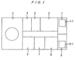
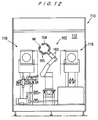
- a substrate plating apparatus for forming interconnections on a semiconductor wafer generally comprises a loading unit 1 for loading a semiconductor wafer, a copper plating chamber 2 for plating a semiconductor wafer with copper, a pair of water cleaning chambers 3, 4 for cleaning a semiconductor wafer with water, a chemical mechanical polishing unit 5 for chemically and mechanically polishing a semiconductor wafer, a pair of water cleaning chambers 6, 7 for cleaning a semiconductor wafer with water, a drying chamber 8 for drying a semiconductor wafer, and an unloading unit 9 for unloading a semiconductor wafer with an interconnection layer thereon.
- the substrate plating apparatus also has a wafer transfer mechanism (not shown) for transferring semiconductor wafers to the chambers 2, 3, 4, the chemical mechanical polishing unit 5, the chambers 6, 7, 8, and the unloading unit 9.
- the loading unit 1, the chambers 2, 3, 4, the chemical mechanical polishing unit 5, the chambers 6, 7, 8, and the unloading unit 9 are combined into a single unitary arrangement as apparatus.
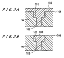
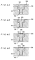
- the substrate plating apparatus operates as follows: The wafer transfer mechanism transfers a semiconductor wafer W on which an interconnection layer has not yet been formed from a wafer cassette 1-1 placed in the loading unit 1 to the copper plating chamber 2. In the copper plating chamber 2, as shown in FIG. 2A, a plated copper layer 103 is formed on a surface of the semiconductor wafer W having an interconnection region composed of an interconnection groove 101 and an interconnection hole (contact hole) 102.
- the semiconductor wafer W is transferred to the water cleaning chambers 3, 4 by the wafer transfer mechanism and cleaned by water in the water cleaning chambers 3, 4.
- the cleaned semiconductor wafer W is transferred to the chemical mechanical polishing unit 5 by the wafer transfer mechanism.
- the chemical mechanical polishing unit 5 removes the unwanted plated copper layer 103 from the surface of the semiconductor wafer W, leaving a portion of the plated copper layer 103 in the interconnection groove 101 and the interconnection hole 102.
- a barrier layer 104 made of TiN or the like is formed on the surface of the semiconductor wafer W, including the inner surfaces of the interconnection groove 101 and the interconnection hole 102, before the plated copper layer 103 is deposited.
- the semiconductor wafer W with the remaining plated copper layer 103 is transferred to the water cleaning chambers 6, 7 by the wafer transfer mechanism and cleaned by water in the water cleaning chambers 6, 7.
- the cleaned semiconductor wafer W is then dried in the drying chamber 8, after which the dried semiconductor wafer W with the remaining plated copper layer 103 serving as an interconnection layer is placed into a wafer cassette 9-1 in the unloading unit 9.
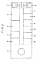
- FIG. 3 shows in plan a substrate plating apparatus for forming interconnections on a semiconductor wafer according to a different design.
- the substrate plating apparatus shown in FIG. 3 differs from the substrate plating apparatus shown in FIG. 1 in that it additionally includes a copper plating chamber 2', a water cleaning chamber 10, a pretreatment chamber 11, and a protective layer plating chamber 12 for forming a protective plated layer on a plated copper layer on a semiconductor wafer.
- the loading unit 1, the chambers 2, 2', 3, 4, the chemical mechanical polishing unit 5, the chambers 6, 7, 8, 10, 11, 12, and the unloading unit 9 are combined into a single unitary arrangement as an apparatus.
- Those parts shown in FIGS. 3 and 4A through 4D which are identical to those shown in FIGS. 1 and 2A, 2B are denoted by identical reference numerals, and will not be described in detail below.
- the substrate plating apparatus shown in FIG. 3 operates as follows: A semiconductor wafer W is supplied from the wafer cassette 1-1 placed in the loading unit 1 successively to the copper plating chambers 2, 2'. In the copper plating chamber 2, 2', as shown in FIG. 4A, a plated copper layer 103 is formed on a surface of a semiconductor wafer W having an interconnection region composed of an interconnection groove 101 and an interconnection hole (contact hole) 102. The two copper plating chambers 2, 2' are employed to allow the semiconductor wafer W to be plated with a copper layer for a long period of time.
- the semiconductor wafer W may be plated with a primary copper layer according to electroplating in the copper plating chamber 2, and then plated with a secondary copper layer according to electroless plating in the copper plating chamber 2'.
- the substrate plating apparatus may have more than two copper plating chambers.
- the semiconductor wafer W with the plated copper layer 103 formed thereon is cleaned by water in the water cleaning chambers 3, 4. Then, as shown in FIG. 4B, the chemical mechanical polishing unit 5 removes the unwanted portion of the plated copper layer 103 from the surface of the semiconductor wafer W, leaving a portion of the plated copper layer 103 in the interconnection groove 101 and the interconnection hole 102.
- the semiconductor wafer W with the remaining plated copper layer 103 is transferred to the water cleaning chamber 10, in which the semiconductor wafer W is cleaned with water. Then, the semiconductor wafer W is transferred to the pretreatment chamber 11, and pretreated therein for the deposition of a protective plated layer. The pretreated semiconductor wafer W is transferred to the protective layer-plating chamber 12.
- a protective plated layer 105 is formed on the plated copper layer 103 in the interconnection region on the semiconductor wafer W.
- the protective plated layer 105 is formed with an alloy of nickel (Ni) and boron (B) by electroless plating.
- the semiconductor wafer W is cleaned by water in the water cleaning chambers 6, 7, dried in the drying chamber 8, and then transferred to the wafer cassette 9-1 in the unloading unit 9.
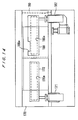
- FIG. 5 shows in plan a substrate plating apparatus for forming interconnections on a semiconductor wafer according to another design.
- the substrate plating apparatus shown in FIG. 5 differs from the substrate plating apparatus shown in FIG. 3 in that it additionally includes a chemical mechanical polishing unit 15, and water cleaning chambers 13, 14.
- the loading unit 1, the chambers 2, 2', 3, 4, 14, the chemical mechanical polishing unit 5, 15, the chambers 6, 7, 8, 10, 11, 12, 13, and the unloading unit 9 are combined into a single unitary arrangement as an apparatus.
- Those parts shown in FIG. 5 which are identical to those shown in FIG. 3 are denoted by identical reference numerals, and will not be described in detail below.
- an upper portion of the protective plated layer 105 deposited on the plated copper layer 103 is polished off to planarize the protective plated layer 105, as shown in FIG. 4D.
- the water cleaning chambers 13, 14 additionally clean the semiconductor wafer W with water.
- FIG. 6 shows in plan a substrate plating apparatus for forming interconnections on a semiconductor wafer according to another design.
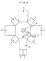
- the substrate plating apparatus includes a robot 16 at its center which has a robot arm 16-1, and also has a copper plating chamber 2, a pair of water cleaning chambers 3, 4, a chemical mechanical polishing unit 5, a pretreatment chamber 11, a protective layer plating chamber 12, a drying chamber 8, and a loading and unloading station 17 which are disposed around the robot 16 and positioned within the reach of the robot arm 16-1.
- a loading unit 1 for loading semiconductor wafers and an unloading unit 9 for unloading semiconductor wafers is disposed adjacent to the loading and unloading station 17.
- the robot 16, the chambers 2, 3, 4, the chemical mechanical polishing unit 5, the chambers 8, 11, 12, the loading and unloading station 17, the loading unit 1, and the unloading unit 9 are combined into a single unitary arrangement as an apparatus.
- the substrate plating apparatus shown in FIG. 6 operates as follows:
- a semiconductor wafer to be plated is transferred from the loading unit 1 to the loading and unloading station 17, from which the semiconductor wafer is received by the robot arm 16-1 and transferred thereby to the copper plating chamber 2.
- a plated copper layer 103 is formed on a surface of the semiconductor wafer which has an interconnection region composed of an interconnection groove 101 and an interconnection hole 102.
- the semiconductor wafer with the plated copper layer 103 formed thereon is transferred by the robot arm 16-1 to the chemical mechanical polishing unit 5.
- the plated copper layer 103 is removed from the surface of the semiconductor wafer W, leaving a portion of the plated copper layer 103 in the interconnection groove 101 and the interconnection hole 102.
- the semiconductor wafer is then transferred by the robot arm 16-1 to the water-cleaning chamber 4, in which the semiconductor wafer is cleaned by water. Thereafter, the semiconductor wafer is transferred by the robot arm 16-1 to the pretreatment chamber 11, in which the semiconductor wafer is pretreated therein for the deposition of a protective plated layer.
- the pretreated semiconductor wafer is transferred by the robot arm 16-1 to the protective layer plating chamber 12.
- a protective plated layer 105 is formed on the plated copper layer 103 in the interconnection region on the semiconductor wafer W, as shown in FIG. 4C.
- the semiconductor wafer with the protective plated layer 105 formed thereon is transferred by the robot arm 16-1 to the water cleaning chamber 4, in which the semiconductor wafer is cleaned by water.
- the cleaned semiconductor wafer is transferred by the robot arm 16-1 to the drying chamber 8, in which the semiconductor wafer is dried.
- the dried semiconductor wafer is transferred by the robot arm 16-1 to the loading and unloading station 17, from which the plated semiconductor wafer is transferred to the unloading unit 9.
- the substrate plating apparatus may have a copper ion concentration analyzer, an oxygen concentration analyzer, a plating additive concentration analyzer, and a plating solution preparing unit for preparing a plating solution based on analyzed results from the analyzers.
- These analyzers and the plating solution preparing unit may be integrally combined with the other components of the substrate plating apparatus into a single arrangement.
- the substrate plating apparatus may have only some of the above analyzers, rather than all of them.
- the substrate plating apparatus may have a copper ion concentration analyzer, an oxidizing agent concentration analyzer, a reducing agent concentration analyzer, a pH measuring unit, and a plating solution preparing unit for preparing a plating solution based on analyzed results from the analyzers and a pH measured by the pH measuring unit.
- These analyzers, the pH-measuring unit, and the plating solution preparing unit may be integrally combined with the other components of the substrate plating apparatus into a single arrangement.
- the substrate plating apparatus may have only some of the above analyzers and the pH measuring unit, rather than all of them.
- the substrate plating apparatus may have a nickel ion concentration analyzer, an oxidizing agent concentration analyzer, a reducing agent concentration analyzer, a pH measuring unit, and a plating solution preparing unit for preparing a plating solution based on analyzed results from the analyzers and a pH measured by the pH measuring unit.
- These analyzers, the pH-measuring unit, and the plating solution preparing unit may be integrally combined with the other components of the substrate plating apparatus into a single arrangement.
- the substrate plating apparatus may have only some of the above analyzers and the pH measuring unit, rather than all of them.
- the substrate plating apparatus may have an ionexchange tower for ion recovery, an activated carbon extraction tower for organic material recovery, a scrubber for processing exhaust gases, and a solidifier for solidifying and discarding discharged liquids.
- the towers, the scrubber, and the solidifier may be integrally combined with the other components of the substrate plating apparatus into a single arrangement.
- the numbers of the plating chambers, water cleaning chambers, and the pretreatment chambers in the substrate plating apparatus shown in FIGS. 1, 3, 5, 6 are illustrative only, and these chambers are not limited to the illustrated numbers.
- the chemical mechanical polishing unit may be associated with a slurry supply unit, a discharged liquid processing unit, and a constant-temperature chamber, which may be integrally combined with the chemical mechanical polishing unit into a single unitary arrangement.
- any one of the illustrated substrate plating apparatus is installed in a clean room, then it is necessary that processed and dried semiconductor wafers should be unloaded and transferred to a next process without exposure to mists, particles, the plating solution, and the cleaning solution in the apparatus. Therefore, particles and mists in a plating area and a cleaning and drying area of the substrate plating apparatus should not be applied to processed and dried semiconductor wafers that are stored in a cassette placed in an unloading area of the substrate plating apparatus.
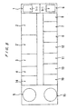
- FIG. 7 shows in plan a substrate plating apparatus for forming interconnections on a semiconductor wafer according to an embodiment of the present invention.
- the substrate plating apparatus shown in FIG. 7 generally comprises a loading and unloading area 20 for transferring wafer cassettes which store semiconductor wafers, a plating area 30 for plating semiconductor wafers, and a cleaning and drying area 40 for cleaning and drying plated semiconductor wafers.
- the cleaning and drying area 40 is positioned between the loading and unloading area 20 and the plating area 30.
- a partition 21 is disposed between the loading and unloading area 20 and the cleaning and drying area 40, and a partition 23 is disposed between the cleaning and drying area 40 and the plating area 30.
- the partition 21 has a passage (not shown) defined therein for transferring semiconductor wafers therethrough between the loading and unloading area 20 and the cleaning and drying area 40, and supports a shutter 22 for opening and closing the passage.
- the partition 23 has a passage (not shown) defined therein for transferring semiconductor wafers therethrough between the cleaning and drying area 40 and the plating area 30, and supports a shutter 24 for opening and closing the passage.
- the cleaning and drying area 40 and the plating area 30 can independently be supplied with and discharge air.
- the substrate plating apparatus shown in FIG. 7 is placed in a clean room, which accommodates semiconductor fabrication facilities.
- the pressures in the loading and unloading area 20, the plating area 30, and the cleaning and drying area 40 are selected as follows:
- the pressure in the loading and unloading area 20 is lower than the pressure in the clean room. Therefore, air does not flow from the plating area 30 into the cleaning and drying area 40, and air does not flow from the cleaning and drying area 40 into the loading and unloading area 20. Furthermore, air does not flow from the loading and unloading area 20 into the clean room.
- the loading and unloading area 20 houses a loading unit 20a and an unloading unit 20b, each accommodating a wafer cassette for storing semiconductor wafers.
- the cleaning and drying area 40 houses two water cleaning units 41 for cleaning plated semiconductor wafers with water, and two drying units 42 for drying plated semiconductor wafers.
- Each of the water cleaning units 41 may comprise a pencil-shaped cleaner with a sponge layer mounted on a front end thereof or a roller with a sponge layer mounted on an outer circumferential surface thereof.
- Each of the drying units 42 may comprise a drier for spinning a semiconductor wafer at a high speed to dehydrate and dry.
- the cleaning and drying area 40 also has a transfer unit (transfer robot) 43 for transferring semiconductor wafers.
- the plating area 30 houses a plurality of pretreatment chambers 31 for pretreating semiconductor wafers prior to being plated, and a plurality of plating chambers 32 for plating semiconductor wafers with copper.
- Each of the pretreatment chambers 31 contains a pretreatment solution bath including sulfuric acid.
- a semiconductor wafer can be pretreated when it is immersed in the pretreatment solution bath in the pretreatment chamber 31.
- Each of the plating chambers 32 contains a plating solution bath including copper sulfate.
- a semiconductor wafer can be plated with copper when it is immersed in the plating solution bath in the plating chamber 32.
- the plating area 30 also has a transfer unit (transfer robot) for transferring semiconductor wafers.
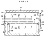
- FIG. 8 shows in side elevation air flows in the substrate plating apparatus.
- fresh air is introduced from the exterior through a duct 46 and forced through high-performance filters 44 by fans from a ceiling 40a into the cleaning and drying area 40 as downward clean air flows around the water cleaning units 41 and the drying units 42.
- Most of the supplied clean air is returned from a floor 40b through a circulation duct 45 to the ceiling 40a, from which the clean air is forced again through the filters 44 by the fans into the cleaning and drying area 40.
- Part of the clean air is discharged from the water cleaning units 41 and the drying units 42 through a duct 52 out of the cleaning and drying area 40.
- the plating area 30 which accommodates the pretreatment chambers 31 and the plating chambers 32, particles are not allowed to be applied to the surfaces of semiconductor wafers even though the plating area 30 is a wet zone.
- downward clean air flows around the pretreatment chambers 31 and the plating chambers 32.
- Fresh air is introduced from the exterior through a duct 39 and forced through high-performance filters 33 by fans from a ceiling 30a into the plating area 30.
- air is discharged from the plating area 30 through a duct 53 at a rate sufficient enough to keep the pressure in the plating area 30 lower than the pressure in the cleaning and drying area 40, and most of the downward clean air introduced into the plating area 30 is circulated through circulation ducts 34, 35.
- the circulation duct 34 extends from the cleaning and drying area 40 and is connected to the filters 33 over the ceiling 30a.
- the circulation duct 35 is disposed in the cleaning and drying area 40 and connected to the pipe 34 in the cleaning and drying area 40.
- the circulating air that has passed around the pretreatment chambers 31 and the plating chambers 32 contains a chemical mist and gases from solution bathes.
- the chemical mist and gases are removed from the circulating air by a scrubber 36 and mist separators 37, 38 which are disposed in the pipe 34 that is connected to the pipe 35.
- the air which circulates from the cleaning and drying area 40 through the scrubber 36 and the mist separators 37, 38 back into the circulation duct 34 over the ceiling 30a is free of any chemical mist and gases.
- the clean air is then forced through the filters 33 by the fans to circulate back into the plating area 30.
- Air containing a chemical mist and gases is also discharged from a plating solution circulating tank 50 and a H 2 SO 4 circulating tank 51 in the plating area 30, through the duct 53.
- An amount of fresh air which is commensurate with the amount of air discharged through the duct 53 is supplied from the duct 39 into the plating chamber 30 under the negative pressure developed therein with respect to the pressure in the clean room.
- the pressure in the loading and unloading area 20 is higher than the pressure in the cleaning and drying area 40 which is higher than the pressure in the plating area 30.
- the shutters 22, 24 are opened, therefore, air flows successively through the loading and unloading area 20, the cleaning and drying area 40, and the plating area 30, as shown in FIG. 9.
- Air discharged from the cleaning and drying area 40 and the plating area 30 flows through the ducts 52, 53 into a common duct 54 (see FIG. 10) which extends out of the clean room.
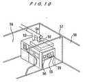
- FIG. 10 shows in perspective the substrate plating apparatus shown in FIG. 7, which is placed in the clean room.
- the loading and unloading area 20 includes a side wall which has a cassette transfer port 55 defined therein and a control panel 56, and which is exposed to a working zone 58 that is compartmented in the clean room by a partition wall 57.
- the partition wall 57 also compartments a utility zone 59 in the clean room in which the substrate plating apparatus is installed.
- Other sidewalls of the substrate plating apparatus are exposed to the utility zone 59 whose air cleanness is lower than the air cleanness in the working zone 58.
- the cleaning and drying area 40 is disposed between the loading and unloading area 20 and the plating area 30.
- the partition 21 is disposed between the loading and unloading area 20 and the cleaning and drying area 40, and the partition 23 is disposed between the cleaning and drying area 40 and the plating area 30.
- a dry semiconductor wafer is loaded from the working zone 58 through the cassette transfer port 55 into the substrate plating apparatus, and then plated in the substrate plating apparatus.
- the plated semiconductor wafer is cleaned and dried, and then unloaded from the substrate plating apparatus through the cassette transfer port 55 into the working zone 58. Consequently, no particles and mist are applied to the surface of the semiconductor wafer, and the working zone 58 which has higher air cleanness than the utility zone 57 is prevented from being contaminated by particles, chemical mists, and cleaning solution mists.
- the substrate plating apparatus has the loading and unloading area 20, the cleaning and drying area 40, and the plating area 30.
- an area accommodating a chemical mechanical polishing unit may be disposed in or adjacent to the plating area 30, and the cleaning and drying area 40 may be disposed in the plating area 30 or between the area accommodating the chemical mechanical polishing unit and the loading and unloading area 20.
- Any of various other suitable area and unit layouts may be employed insofar as a dry semiconductor wafer can be loaded into the substrate plating apparatus, and a plated semiconductor wafer can be cleaned and dried, and thereafter unloaded from the substrate plating apparatus.
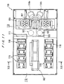
- FIGS. 11 through 15 show a substrate plating apparatus for forming interconnections on a semiconductor wafer according to yet another design.
- the substrate plating apparatus generally denoted by 110, has a contaminated zone 112 and a clean zone 113 divided by a partition 111.
- the contaminated zone 112 and the clean zone 113 can independently be supplied with and discharge air.
- the pressure in the clean zone 113 is higher than the pressure in the contaminated zone 112.
- the clean zone 113 accommodates a loading unit 114a, an unloading unit 114b, two water cleaning and drying units 160 for cleaning and drying plated semiconductor wafers, and a transfer unit (transfer robot) 161 for transferring semiconductor wafers.
- the contaminated zone 112 accommodates two pretreatment chambers 118 for pretreating semiconductor wafers by pretreating solution bathes, a plurality of plating chambers 119 for plating semiconductor wafers with copper by plating solution bathes, and a transfer unit (transfer robot) 162 for transferring semiconductor wafers.
- the pretreatment chambers 118 and the plating chambers 119 are similar in structure and operation to those according the previous embodiments.
- the transfer unit 162 disposed in the contaminated zone 112 comprises a six-axis robot, for example, having a plurality of interconnected arms 163 with an openable and closable grip hand 164 mounted on a tip end of the arms 163.
- the grip hand 164 is in the form of a ring having a plurality of rotatable rollers 163 mounted on an inner circumferential surface thereof.
- a loading stage 167 having a plurality (four are illustrated) of support bases 166 is mounted in the clean zone 113 adjacent to the partition 111.
- the transfer unit 161 in the clean zone 113 holds a semiconductor wafer W to be plated and places the semiconductor wafer W onto the support bases 166 of the loading stage 167, and then the transfer unit 162 in the contaminated zone 112 picks up the semiconductor wafer W from the support bases 166.
- a partition wall 170 is disposed between the loading stage 167 and the partition 111.
- the partition wall 170 has an opening 170a defined therein for passage of the grip hand 164 of the transfer unit 162 therethrough and a shutter 172 actuatable by a cylinder 171 for opening and closing the opening 170a.
- the partition 111 also has an opening 111a defined therein for passage of the grip hand 164 of the transfer unit 162 therethrough.
- a roughly cleaning chamber 183 is positioned adjacent to the partition 111 in juxtaposed relation to the loading stage 167.
- the roughly cleaning chamber 183 is defined as a box by a rear partition wall 180 contiguous to the partition wall 170, a front partition wall 181 of a substantially C-shape joined to the rear partition wall 180, and a ceiling 182 (see FIG. 15).
- the roughly cleaning chamber 183 accommodates an unloading stage 185 having a plurality of (four are illustrated) support bases 184.
- the unloading stage 185 is identical in structure to the loading stage 167.
- two vertically spaced arrays of ejection nozzles 186 for ejecting a cleaning solution are disposed in the roughly cleaning chamber 183.
- the rear partition wall 180 has an opening 180a defined therein for passage of the grip hand 164 of the transfer unit 162 in the contaminated zone 112 therethrough and a shutter 188 actuatable by a cylinder 187 for opening and closing the opening 180a.
- the front partition wall 181 has an opening 181a defined therein for passage of a grip hand of the transfer unit 161 in the clean zone 113 therethrough and a shutter 190 actuatable by a cylinder 189 for opening and closing the opening 181a.
- the opening 111a in the partition 111 extends from a position behind the loading stage 167 all the way to a position behind the roughly cleaning chamber 183 for allowing the grip hand 164 of the transfer unit 162 to move freely toward and away from the openings 170a, 180a.
- the shutter 188 has a recess 188a defined in an upper edge thereof for passage therethrough of only the arms 163 of the transfer unit 162.
- the grip hand 164 of the transfer unit 162 in the contaminated zone 112 can be inserted through the recess 188a into the roughly cleaning chamber 183. Therefore, the grip hand 164 and a plated semiconductor wafer W gripped thereby can be roughly cleaned in the roughly cleaning chamber 183. After the grip hand 164 and the plated semiconductor wafer W gripped thereby are roughly cleaned, the grip hand 164 places the semiconductor wafer W onto the support bases 184 of the unloading stage 185. The semiconductor wafer W placed on the support bases 184 is roughly cleaned again, and thereafter picked up by the transfer unit 161 in the clean zone 113.
- the shutter 188 is opened by being lowered by the cylinder 187, and a plated semiconductor wafer W gripped by the grid hand 164 of the transfer unit 162 is introduced into the roughly cleaning chamber 183.
- the shutter 188 is then lifted, and with the arms 163 of the transfer unit 162 being inserted through the recess 188a, the ejection nozzles 186 eject a cleaning solution to the semiconductor wafer W for thereby roughly cleaning the grip hand 164 and the semiconductor wafer W.
- the roughly cleaned semiconductor wafer W is placed onto the support bases 184, and the grip hand 164 is retracted out of the roughly cleaning chamber 183. Then, the shutter 188 is fully closed.
- the ejection nozzles 186 eject a cleaning solution again to the semiconductor wafer W on the support bases 184 for roughly cleaning the semiconductor wafer W again.
- the shutter 190 is opened, and the grip hand of the transfer unit 161 in the clean zone 113 is inserted into the roughly cleaning chamber 183. After the grip hand of the transfer unit 161 picks up the semiconductor wafer W and removes the semiconductor wafer W from the roughly cleaning chamber 183, the shutter 190 is closed.
- the grip hand 164 of the transfer unit 162 in the contaminated zone 112 is roughly cleaned together with the plated semiconductor wafer W, the plating solution is prevented from being applied to and deposited on the grip hand 164. Consequently, the grip hand 164 does not transfer any substantial contamination to the transfer unit 161 in the clean zone 113.
- the clean zone 113 accommodates the loading stage 167 and the roughly cleaning chamber 183, which houses the unloading stage 185.
- the loading stage 167 and the roughly cleaning chamber 183 which houses the unloading stage 185 may be disposed in the contaminated zone 112.
- the present invention is applied to the substrate plating apparatus for plating a semiconductor wafer.
- the principles of the present invention are also applicable to a substrate plating apparatus for plating a substrate other than a semiconductor wafer.
- a region on a substrate plated by the substrate plating apparatus is not limited to an interconnection region on the substrate.
- the substrate plating apparatus may be used to plate substrates with a metal other than copper.
Landscapes
- Engineering & Computer Science (AREA)
- Physics & Mathematics (AREA)
- Condensed Matter Physics & Semiconductors (AREA)
- General Physics & Mathematics (AREA)
- Manufacturing & Machinery (AREA)
- Computer Hardware Design (AREA)
- Microelectronics & Electronic Packaging (AREA)
- Power Engineering (AREA)
- Chemical & Material Sciences (AREA)
- Sustainable Development (AREA)
- Life Sciences & Earth Sciences (AREA)
- Chemical Kinetics & Catalysis (AREA)
- Electrochemistry (AREA)
- Materials Engineering (AREA)
- Metallurgy (AREA)
- Organic Chemistry (AREA)
- Internal Circuitry In Semiconductor Integrated Circuit Devices (AREA)
- Cleaning Or Drying Semiconductors (AREA)
- Electroplating Methods And Accessories (AREA)
- Mechanical Treatment Of Semiconductor (AREA)
Claims (12)
- Appareil de revêtement de substrat comprenant :une section de chargement et de déchargement (20) pour transférer une cassette qui contient un substrat ;une section de revêtement (30) pour le revêtement dudit substrat, comprenant une première unité de revêtement (32) pour former une couche revêtue sur une surface du substrat comprenant une région d'interconnexion ;une première unité de polissage chimique et mécanique pour le polissage chimique et mécanique dudit substrat pour éliminer une couche revêtue non voulue de la surface du substrat en laissant une partie de la couche revêtue dans ladite région d'interconnexion ; etune section de nettoyage et de séchage (40) comprenant une unité de nettoyage (41) pour nettoyer ledit substrat une fois que ladite couche revêtue est formée ou que ledit substrat est poli chimiquement et mécaniquement, et une unité de séchage (42) pour sécher ledit substrat une fois que ledit substrat est nettoyé ;ladite section de nettoyage et de séchage (40) étant disposée entre ladite section de chargement et de déchargement (20) et ladite section de revêtement (30) ;ledit appareil de revêtement de substrat étant caractérisé par :une première paroi de séparation (21) disposée entre ladite section de chargement et de déchargement (20) et ladite section de nettoyage et de séchage (40) et ayant un passage défini à l'intérieur pour transférer un substrat entre ladite section de chargement et de déchargement (20) et ladite section de nettoyage et de séchage (40) ; etune deuxième paroi de séparation (23) disposée entre ladite section de nettoyage et de séchage (40) et ladite région de revêtement (30) et ayant un passage défini à l'intérieur pour transférer ledit substrat entre ladite section de nettoyage et de séchage (40) et ladite section de revêtement (30).
- Appareil de revêtement de substrat selon la revendication 1, comprenant en outre :un dispositif de transfert de substrat pour transférer ledit substrat vers et depuis chacune de ladite première unité de revêtement (32), ladite première unité de polissage chimique et mécanique, ladite unité de nettoyage (41), et ladite unité de séchage (42);ladite première unité de revêtement (32), ladite première unité de polissage chimique et mécanique, ladite unité de nettoyage (41), ladite unité de séchage (42), et ledit dispositif de transfert de substrat étant combinés dans un agencement unitaire unique.
- Appareil de revêtement de substrat selon la revendication 2, comprenant en outre :une deuxième unité de revêtement (32) pour former une couche revêtue de protection sur ladite partie de la couche revêtue dans ladite région d'interconnexion après que la couche revêtue non voulue soit retirée de la surface du substrat, ladite deuxième unité de revêtement (32) étant contenue dans ledit agencement unitaire unique.
- Appareil de revêtement de substrat selon la revendication 2, comprenant en outre :une deuxième unité de polissage chimique et mécanique pour polir chimiquement et mécaniquement ledit substrat pour rendre plane ladite couche revêtue de protection formée sur ladite partie de la couche revêtue dans ladite région d'interconnexion, ladite deuxième unité de polissage chimique et mécanique étant contenue dans ledit agencement unitaire unique.
- Appareil de revêtement de substrat selon la revendication 2, comprenant en outre :une installation d'évacuation pour évacuer une solution de nettoyage utilisée par ladite unité de nettoyage pour nettoyer ledit substrat, ladite installation d'évacuation étant contenue dans ledit agencement unitaire unique.
- Appareil de revêtement de substrat selon la revendication 1, dans lequel ledit dispositif de transfert de substrat comprend un robot ayant un bras, ladite première unité de revêtement (32), ladite première unité de polissage chimique et mécanique, ladite unité de nettoyage (41), et ladite unité de séchage (42) étant disposé à portée dudit bras.
- Appareil de revêtement de substrat selon la revendication 2, comprenant en outre :un dispositif d'analyse de concentration pour analyser les concentrations des composants d'une solution de revêtement utilisée par ladite première unité de revêtement (32) pour former ladite couche revêtue ; etun dispositif de préparation de solution de revêtement pour préparer une solution de revêtement basée sur les concentrations analysées par ledit dispositif d'analyse de concentration ;ledit dispositif d'analyse de concentration et lesdits dispositifs de préparation de solution de revêtement étant contenus dans ledit agencement unitaire unique.
- Appareil de revêtement de substrat selon la revendication 1, comprenant en outre :un premier volet (22) monté de manière mobile pour ouvrir et fermer ledit passage défini dans ladite première paroi de séparation (21) ; etun deuxième volet (24) monté de manière mobile pour ouvrir et fermer ledit passage défini dans ladite deuxième paroi de séparation (23).
- Appareil de revêtement de substrat selon la revendication 1, qui est installé dans une salle blanche, où les pressions dans ladite section de chargement et de déchargement (20), ladite section de revêtement (30), et ladite section de nettoyage et de séchage (40) sont choisies de sorte que la pression dans ladite section de chargement et de déchargement (20) soit supérieure à la pression dans ladite section de nettoyage et de séchage (30) qui est supérieure à la pression dans ladite section de revêtement (40), ladite pression dans ladite section de chargement et de déchargement (20) étant inférieure à une pression dans ladite salle blanche.
- Appareil de revêtement de substrat selon la revendication 1, dans lequel une chambre de nettoyage grossier est positionnée de manière adjacente à ladite deuxième paroi de séparation (23) pour nettoyer grossièrement ledit substrat après revêtement avec une poignée de préhension dudit dispositif de transfert.
- Appareil de revêtement de substrat selon la revendication 1, dans lequel ladite section de revêtement reçoit une chambre de pré-traitement (31).
- Appareil de revêtement de substrat selon la revendication 1, dans lequel un écoulement descendant d'air pur s'écoule dans lesdites sections (20, 30, 40).
Applications Claiming Priority (12)
| Application Number | Priority Date | Filing Date | Title |
|---|---|---|---|
| JP270493/97 | 1997-09-17 | ||
| JP27049397 | 1997-09-17 | ||
| JP27049397 | 1997-09-17 | ||
| JP7137098 | 1998-03-05 | ||
| JP7137098 | 1998-03-05 | ||
| JP71370/98 | 1998-03-05 | ||
| JP9697498 | 1998-03-26 | ||
| JP09697498A JP3830272B2 (ja) | 1998-03-05 | 1998-03-26 | 基板のめっき装置 |
| JP96974/98 | 1998-03-26 | ||
| JP205138/98 | 1998-07-21 | ||
| JP20513898A JPH11154653A (ja) | 1997-09-17 | 1998-07-21 | 基板メッキ装置 |
| JP20513898 | 1998-07-21 |
Publications (3)
| Publication Number | Publication Date |
|---|---|
| EP0903774A2 EP0903774A2 (fr) | 1999-03-24 |
| EP0903774A3 EP0903774A3 (fr) | 2004-01-21 |
| EP0903774B1 true EP0903774B1 (fr) | 2008-01-30 |
Family
ID=27465359
Family Applications (1)
| Application Number | Title | Priority Date | Filing Date |
|---|---|---|---|
| EP98117633A Expired - Lifetime EP0903774B1 (fr) | 1997-09-17 | 1998-09-17 | Dispositif de revêtement de substrat |
Country Status (5)
| Country | Link |
|---|---|
| US (3) | US6294059B1 (fr) |
| EP (1) | EP0903774B1 (fr) |
| KR (1) | KR100554855B1 (fr) |
| DE (1) | DE69839066T2 (fr) |
| TW (1) | TW405158B (fr) |
Families Citing this family (66)
| Publication number | Priority date | Publication date | Assignee | Title |
|---|---|---|---|---|
| US6276072B1 (en) | 1997-07-10 | 2001-08-21 | Applied Materials, Inc. | Method and apparatus for heating and cooling substrates |
| AU3553599A (en) * | 1998-04-13 | 1999-11-01 | Acm Research, Inc. | Method and apparatus for enhancing adhesion between barrier layer and metal layer formed by plating |
| KR100654413B1 (ko) * | 1998-04-30 | 2006-12-05 | 가부시키가이샤 에바라 세이사꾸쇼 | 기판의 도금방법 |
| WO2000010200A1 (fr) * | 1998-08-11 | 2000-02-24 | Ebara Corporation | Procede et appareil de metallisation de plaquettes |
| US7204917B2 (en) | 1998-12-01 | 2007-04-17 | Novellus Systems, Inc. | Workpiece surface influencing device designs for electrochemical mechanical processing and method of using the same |
| US6409904B1 (en) | 1998-12-01 | 2002-06-25 | Nutool, Inc. | Method and apparatus for depositing and controlling the texture of a thin film |
| US6328872B1 (en) * | 1999-04-03 | 2001-12-11 | Nutool, Inc. | Method and apparatus for plating and polishing a semiconductor substrate |
| KR100665745B1 (ko) * | 1999-01-26 | 2007-01-09 | 가부시키가이샤 에바라 세이사꾸쇼 | 구리도금방법 및 그 장치 |
| US7192494B2 (en) * | 1999-03-05 | 2007-03-20 | Applied Materials, Inc. | Method and apparatus for annealing copper films |
| US6551488B1 (en) * | 1999-04-08 | 2003-04-22 | Applied Materials, Inc. | Segmenting of processing system into wet and dry areas |
| US6585876B2 (en) | 1999-04-08 | 2003-07-01 | Applied Materials Inc. | Flow diffuser to be used in electro-chemical plating system and method |
| US7022211B2 (en) | 2000-01-31 | 2006-04-04 | Ebara Corporation | Semiconductor wafer holder and electroplating system for plating a semiconductor wafer |
| JP2000331975A (ja) * | 1999-05-19 | 2000-11-30 | Ebara Corp | ウエハ洗浄装置 |
| KR20020019056A (ko) * | 1999-06-01 | 2002-03-09 | 히가시 데쓰로 | 반도체 장치의 제조 방법 및 제조 장치 |
| KR100637890B1 (ko) * | 1999-07-08 | 2006-10-23 | 가부시키가이샤 에바라 세이사꾸쇼 | 도금장치 및 도금방법 및 도금처리설비 |
| US6423200B1 (en) | 1999-09-30 | 2002-07-23 | Lam Research Corporation | Copper interconnect seed layer treatment methods and apparatuses for treating the same |
| WO2001027983A1 (fr) * | 1999-10-15 | 2001-04-19 | Ebara Corporation | Procede et appareil destines a former une interconnexion |
| US6660139B1 (en) | 1999-11-08 | 2003-12-09 | Ebara Corporation | Plating apparatus and method |
| JP3367655B2 (ja) * | 1999-12-24 | 2003-01-14 | 島田理化工業株式会社 | めっき処理装置及びめっき処理方法 |
| WO2001048800A1 (fr) * | 1999-12-24 | 2001-07-05 | Ebara Corporation | Procede et appareil de traitement de tranche de semi-conducteur |
| US6457199B1 (en) * | 2000-10-12 | 2002-10-01 | Lam Research Corporation | Substrate processing in an immersion, scrub and dry system |
| EP1204139A4 (fr) * | 2000-04-27 | 2010-04-28 | Ebara Corp | Dispositif de support et de rotation et dispositif de traitement de substrat de semi-conducteur |
| US6634370B2 (en) * | 2000-05-08 | 2003-10-21 | Tokyo Electron Limited | Liquid treatment system and liquid treatment method |
| US6689257B2 (en) * | 2000-05-26 | 2004-02-10 | Ebara Corporation | Substrate processing apparatus and substrate plating apparatus |
| US6645550B1 (en) * | 2000-06-22 | 2003-11-11 | Applied Materials, Inc. | Method of treating a substrate |
| US6811658B2 (en) * | 2000-06-29 | 2004-11-02 | Ebara Corporation | Apparatus for forming interconnects |
| US6413390B1 (en) * | 2000-10-02 | 2002-07-02 | Advanced Micro Devices, Inc. | Plating system with remote secondary anode for semiconductor manufacturing |
| JP4644926B2 (ja) * | 2000-10-13 | 2011-03-09 | ソニー株式会社 | 半導体製造装置および半導体装置の製造方法 |
| US6617867B2 (en) * | 2000-11-29 | 2003-09-09 | Teradyne, Inc. | Mechanism for clamping device interface board to peripheral |
| EP1405336A2 (fr) * | 2000-12-04 | 2004-04-07 | Ebara Corporation | Procede de traitement de substrat |
| US20020139684A1 (en) * | 2001-04-02 | 2002-10-03 | Mitsubishi Denki Kabushiki Kaisha | Plating system, plating method, method of manufacturing semiconductor device using the same, and method of manufacturing printed board using the same |
| US6572755B2 (en) | 2001-04-11 | 2003-06-03 | Speedfam-Ipec Corporation | Method and apparatus for electrochemically depositing a material onto a workpiece surface |
| WO2002083995A1 (fr) * | 2001-04-12 | 2002-10-24 | Arthur, Keigler | Procede et dispositif de regulation de l'ecoulement de fluides |
| US6703316B2 (en) * | 2001-04-27 | 2004-03-09 | Kabushiki Kaisha Kobe Seiko Sho | Method and system for processing substrate |
| JP2003027280A (ja) * | 2001-07-18 | 2003-01-29 | Ebara Corp | めっき装置 |
| TW554069B (en) * | 2001-08-10 | 2003-09-21 | Ebara Corp | Plating device and method |
| EP1418619A4 (fr) * | 2001-08-13 | 2010-09-08 | Ebara Corp | Dispositif a semiconducteur, son procede de production et solution de galvanoplastie |
| TWI274393B (en) * | 2002-04-08 | 2007-02-21 | Acm Res Inc | Electropolishing and/or electroplating apparatus and methods |
| MXPA03010817A (es) * | 2002-04-10 | 2004-03-22 | Sony Corp | Aparato de registro de datos, metodo de registro de datos, medio de almacenamiento de programa, y programa. |
| US7252714B2 (en) * | 2002-07-16 | 2007-08-07 | Semitool, Inc. | Apparatus and method for thermally controlled processing of microelectronic workpieces |
| JP3827627B2 (ja) * | 2002-08-13 | 2006-09-27 | 株式会社荏原製作所 | めっき装置及びめっき方法 |
| EP1577421A1 (fr) * | 2002-11-15 | 2005-09-21 | Ebara Corporation | Dispositif et procede de traitement de substrat |
| US6939403B2 (en) | 2002-11-19 | 2005-09-06 | Blue29, Llc | Spatially-arranged chemical processing station |
| US7311810B2 (en) * | 2003-04-18 | 2007-12-25 | Applied Materials, Inc. | Two position anneal chamber |
| JP2004339579A (ja) * | 2003-05-16 | 2004-12-02 | Ebara Corp | 電解処理装置及び方法 |
| WO2004107422A2 (fr) * | 2003-05-27 | 2004-12-09 | Ebara Corporation | Appareil et procede d'electrodeposition |
| US7413983B2 (en) * | 2003-06-13 | 2008-08-19 | Ebara Corporation | Plating method including pretreatment of a surface of a base metal |
| JP2005044910A (ja) * | 2003-07-24 | 2005-02-17 | Ebara Corp | 配線形成方法及び配線形成装置 |
| JP2005082843A (ja) * | 2003-09-05 | 2005-03-31 | Ebara Corp | 電解液管理方法及び管理装置 |
| US20050208201A1 (en) * | 2003-11-07 | 2005-09-22 | Makoto Kubota | Method and apparatus for determining the concentrations of additives in a plating solution |
| US20050236268A1 (en) * | 2004-04-21 | 2005-10-27 | Koji Mishima | Substrate processing apparatus |
| US20080207005A1 (en) * | 2005-02-15 | 2008-08-28 | Freescale Semiconductor, Inc. | Wafer Cleaning After Via-Etching |
| WO2007087831A1 (fr) * | 2006-02-03 | 2007-08-09 | Freescale Semiconductor, Inc. | Suspension cmp écran 'universelle' utilisable avec des diélectriques intercouches à faible constante diélectrique |
| US7803719B2 (en) | 2006-02-24 | 2010-09-28 | Freescale Semiconductor, Inc. | Semiconductor device including a coupled dielectric layer and metal layer, method of fabrication thereof, and passivating coupling material comprising multiple organic components for use in a semiconductor device |
| WO2007095973A1 (fr) * | 2006-02-24 | 2007-08-30 | Freescale Semiconductor, Inc. | Système intégré de traitement de substrat à semi-conducteurs par dépôt métallique en phase liquide |
| US7694688B2 (en) * | 2007-01-05 | 2010-04-13 | Applied Materials, Inc. | Wet clean system design |
| WO2009007793A1 (fr) * | 2007-07-09 | 2009-01-15 | Freescale Semiconductor, Inc. | Composition de couche de couplage pour dispositif semi-conducteur, ce dispositif et son appareil de fabrication, et procédé de formation de la couche de couplage |
| CN102371525B (zh) * | 2010-08-19 | 2014-09-24 | 中芯国际集成电路制造(上海)有限公司 | 抛光装置 |
| KR102003677B1 (ko) * | 2011-02-10 | 2019-07-26 | 주식회사 케이씨텍 | 반도체 기판 세정 장치 |
| EP2502877B1 (fr) * | 2011-03-23 | 2013-10-02 | Patek Philippe SA Genève | Procédé de fabrication d'une pièce composite notamment pour mouvement d'horlogerie |
| US9388504B2 (en) | 2013-03-26 | 2016-07-12 | Ebara Corporation | Plating apparatus and plating method |
| JP6239417B2 (ja) | 2014-03-24 | 2017-11-29 | 株式会社荏原製作所 | 基板処理装置 |
| CN105097651B (zh) * | 2014-05-07 | 2019-12-24 | 盛美半导体设备(上海)有限公司 | 镀铜减薄一体化装置 |
| US20170370017A1 (en) * | 2016-06-27 | 2017-12-28 | Tel Nexx, Inc. | Wet processing system and method of operating |
| WO2022086186A1 (fr) * | 2020-10-20 | 2022-04-28 | 삼성전자 주식회사 | Dispositif électronique comprenant un boîtier externe plaqué avec un élément conducteur et son procédé de fabrication |
| CN115404467B (zh) * | 2022-09-02 | 2024-01-09 | 江苏芯梦半导体设备有限公司 | 全自动化学镀系统及化学镀方法 |
Family Cites Families (36)
| Publication number | Priority date | Publication date | Assignee | Title |
|---|---|---|---|---|
| US3649509A (en) * | 1969-07-08 | 1972-03-14 | Buckbee Mears Co | Electrodeposition systems |
| US4324629A (en) * | 1979-06-19 | 1982-04-13 | Hitachi, Ltd. | Process for regenerating chemical copper plating solution |
| JPS6014244A (ja) * | 1983-07-06 | 1985-01-24 | Fujitsu Ltd | マスク洗浄装置 |
| US4609565A (en) * | 1984-10-10 | 1986-09-02 | Mobil Solar Energy Corporation | Method of fabricating solar cells |
| US4924890A (en) * | 1986-05-16 | 1990-05-15 | Eastman Kodak Company | Method and apparatus for cleaning semiconductor wafers |
| US4774101A (en) * | 1986-12-10 | 1988-09-27 | American Telephone And Telegraph Company, At&T Technologies, Inc. | Automated method for the analysis and control of the electroless metal plating solution |
| US4789438A (en) | 1987-06-23 | 1988-12-06 | Olin Corporation | Cathode surface treatment for electroforming metallic foil or strip |
| US5092975A (en) * | 1988-06-14 | 1992-03-03 | Yamaha Corporation | Metal plating apparatus |
| JPH0414222A (ja) * | 1990-05-07 | 1992-01-20 | Hitachi Ltd | 半導体装置の製造方法及び製造装置 |
| JPH0344058A (ja) * | 1989-07-11 | 1991-02-25 | Hitachi Ltd | 半導体装置の製造方法および製造装置 |
| US5338362A (en) * | 1992-08-29 | 1994-08-16 | Tokyo Electron Limited | Apparatus for processing semiconductor wafer comprising continuously rotating wafer table and plural chamber compartments |
| US5368715A (en) | 1993-02-23 | 1994-11-29 | Enthone-Omi, Inc. | Method and system for controlling plating bath parameters |
| JP3213113B2 (ja) | 1993-03-15 | 2001-10-02 | 株式会社荏原製作所 | はんだめっき液自動管理装置 |
| JP3437600B2 (ja) | 1993-03-15 | 2003-08-18 | 株式会社荏原製作所 | はんだめっき液自動分析方法及び装置 |
| US5885138A (en) | 1993-09-21 | 1999-03-23 | Ebara Corporation | Method and apparatus for dry-in, dry-out polishing and washing of a semiconductor device |
| JP3583490B2 (ja) | 1994-12-28 | 2004-11-04 | 株式会社荏原製作所 | ポリッシング装置 |
| JP3315544B2 (ja) | 1994-11-29 | 2002-08-19 | 株式会社荏原製作所 | 半導体ウエハ研磨装置および方法 |
| US5827110A (en) | 1994-12-28 | 1998-10-27 | Kabushiki Kaisha Toshiba | Polishing facility |
| JP3583491B2 (ja) | 1994-12-28 | 2004-11-04 | 株式会社荏原製作所 | ポリッシング装置および方法 |
| JPH08187660A (ja) | 1994-12-28 | 1996-07-23 | Ebara Corp | ポリッシング装置 |
| KR100390293B1 (ko) | 1993-09-21 | 2003-09-02 | 가부시끼가이샤 도시바 | 폴리싱장치 |
| JP3420849B2 (ja) | 1993-09-21 | 2003-06-30 | 株式会社東芝 | ポリッシング装置及び方法 |
| US5415890A (en) * | 1994-01-03 | 1995-05-16 | Eaton Corporation | Modular apparatus and method for surface treatment of parts with liquid baths |
| DE19544328B4 (de) | 1994-11-29 | 2014-03-20 | Ebara Corp. | Poliervorrichtung |
| JP3803130B2 (ja) | 1994-12-06 | 2006-08-02 | 株式会社荏原製作所 | ポリッシング装置及びポリッシング方法 |
| JP3044277B2 (ja) * | 1994-12-21 | 2000-05-22 | 信越半導体株式会社 | ウェーハの洗浄及び洗浄乾燥装置 |
| JP3579802B2 (ja) * | 1994-12-27 | 2004-10-20 | 秋田製錬株式会社 | 陰極板の自動搬送処理装置 |
| JPH08222616A (ja) * | 1995-02-13 | 1996-08-30 | Dainippon Screen Mfg Co Ltd | 基板処理装置 |
| US5830272A (en) * | 1995-11-07 | 1998-11-03 | Sputtered Films, Inc. | System for and method of providing a controlled deposition on wafers |
| US5891513A (en) * | 1996-01-16 | 1999-04-06 | Cornell Research Foundation | Electroless CU deposition on a barrier layer by CU contact displacement for ULSI applications |
| US5723387A (en) | 1996-07-22 | 1998-03-03 | Industrial Technology Research Institute | Method and apparatus for forming very small scale Cu interconnect metallurgy on semiconductor substrates |
| TW419785B (en) | 1996-11-28 | 2001-01-21 | Ind Tech Res Inst | Method and apparatus for forming very small scale metal interconnect on semiconductor substrates |
| US6017437A (en) * | 1997-08-22 | 2000-01-25 | Cutek Research, Inc. | Process chamber and method for depositing and/or removing material on a substrate |
| US6110011A (en) | 1997-11-10 | 2000-08-29 | Applied Materials, Inc. | Integrated electrodeposition and chemical-mechanical polishing tool |
| US5897426A (en) | 1998-04-24 | 1999-04-27 | Applied Materials, Inc. | Chemical mechanical polishing with multiple polishing pads |
| US6254760B1 (en) | 1999-03-05 | 2001-07-03 | Applied Materials, Inc. | Electro-chemical deposition system and method |
-
1998
- 1998-09-16 TW TW087115386A patent/TW405158B/zh not_active IP Right Cessation
- 1998-09-17 US US09/154,895 patent/US6294059B1/en not_active Expired - Lifetime
- 1998-09-17 DE DE69839066T patent/DE69839066T2/de not_active Expired - Fee Related
- 1998-09-17 KR KR1019980038368A patent/KR100554855B1/ko not_active Expired - Lifetime
- 1998-09-17 EP EP98117633A patent/EP0903774B1/fr not_active Expired - Lifetime
-
2001
- 2001-09-05 US US09/945,711 patent/US6929722B2/en not_active Expired - Lifetime
-
2004
- 2004-02-26 US US10/786,110 patent/US20040163947A1/en not_active Abandoned
Also Published As
| Publication number | Publication date |
|---|---|
| US6294059B1 (en) | 2001-09-25 |
| DE69839066D1 (de) | 2008-03-20 |
| KR100554855B1 (ko) | 2006-06-14 |
| US20020005359A1 (en) | 2002-01-17 |
| EP0903774A3 (fr) | 2004-01-21 |
| TW405158B (en) | 2000-09-11 |
| US20040163947A1 (en) | 2004-08-26 |
| DE69839066T2 (de) | 2009-01-22 |
| KR19990029870A (ko) | 1999-04-26 |
| EP0903774A2 (fr) | 1999-03-24 |
| US6929722B2 (en) | 2005-08-16 |
Similar Documents
| Publication | Publication Date | Title |
|---|---|---|
| EP0903774B1 (fr) | Dispositif de revêtement de substrat | |
| JP3883378B2 (ja) | めっき装置及び方法 | |
| KR100597024B1 (ko) | 기판의 도금장치 | |
| JP3171807B2 (ja) | 洗浄装置及び洗浄方法 | |
| KR100824759B1 (ko) | 기판처리장치 및 기판도금장치 | |
| US6689216B2 (en) | Plating apparatus and plating liquid removing method | |
| US6936302B2 (en) | Electroless Ni-B plating liquid, electronic device and method for manufacturing the same | |
| JPS6347137B2 (fr) | ||
| US20030131494A1 (en) | Apparatus and method for rinsing substrates | |
| JPH11154653A5 (fr) | ||
| JPH11154653A (ja) | 基板メッキ装置 | |
| JP3830272B2 (ja) | 基板のめっき装置 | |
| KR100694563B1 (ko) | 기판도금장치 | |
| JP4064132B2 (ja) | 基板処理装置及び基板処理方法 | |
| JPH10154688A (ja) | 洗浄装置及び洗浄方法 | |
| JPH10209109A (ja) | 洗浄装置及び洗浄方法 | |
| JP3171821B2 (ja) | 洗浄装置及び洗浄方法 | |
| JP4112879B2 (ja) | 電解処理装置 | |
| JP4044223B2 (ja) | 基板メッキ装置 | |
| JP2596212B2 (ja) | 半導体装置の湿式処理装置 | |
| JP2000109994A5 (fr) | ||
| JP2000109999A5 (fr) | ||
| JPH04333234A (ja) | 洗浄装置及び洗浄方法 |
Legal Events
| Date | Code | Title | Description |
|---|---|---|---|
| PUAI | Public reference made under article 153(3) epc to a published international application that has entered the european phase |
Free format text: ORIGINAL CODE: 0009012 |
|
| AK | Designated contracting states |
Kind code of ref document: A2 Designated state(s): AT BE CH CY DE DK ES FI FR GB GR IE IT LI LU MC NL PT SE |
|
| AX | Request for extension of the european patent |
Free format text: AL;LT;LV;MK;RO;SI |
|
| PUAL | Search report despatched |
Free format text: ORIGINAL CODE: 0009013 |
|
| AK | Designated contracting states |
Kind code of ref document: A3 Designated state(s): AT BE CH CY DE DK ES FI FR GB GR IE IT LI LU MC NL PT SE |
|
| AX | Request for extension of the european patent |
Extension state: AL LT LV MK RO SI |
|
| 17P | Request for examination filed |
Effective date: 20040720 |
|
| AKX | Designation fees paid |
Designated state(s): DE FR GB |
|
| 17Q | First examination report despatched |
Effective date: 20050928 |
|
| GRAP | Despatch of communication of intention to grant a patent |
Free format text: ORIGINAL CODE: EPIDOSNIGR1 |
|
| GRAS | Grant fee paid |
Free format text: ORIGINAL CODE: EPIDOSNIGR3 |
|
| GRAA | (expected) grant |
Free format text: ORIGINAL CODE: 0009210 |
|
| AK | Designated contracting states |
Kind code of ref document: B1 Designated state(s): DE FR GB |
|
| REG | Reference to a national code |
Ref country code: GB Ref legal event code: FG4D |
|
| REF | Corresponds to: |
Ref document number: 69839066 Country of ref document: DE Date of ref document: 20080320 Kind code of ref document: P |
|
| EN | Fr: translation not filed | ||
| PLBE | No opposition filed within time limit |
Free format text: ORIGINAL CODE: 0009261 |
|
| STAA | Information on the status of an ep patent application or granted ep patent |
Free format text: STATUS: NO OPPOSITION FILED WITHIN TIME LIMIT |
|
| PGFP | Annual fee paid to national office [announced via postgrant information from national office to epo] |
Ref country code: GB Payment date: 20080904 Year of fee payment: 11 |
|
| 26N | No opposition filed |
Effective date: 20081031 |
|
| PGFP | Annual fee paid to national office [announced via postgrant information from national office to epo] |
Ref country code: DE Payment date: 20080929 Year of fee payment: 11 |
|
| PG25 | Lapsed in a contracting state [announced via postgrant information from national office to epo] |
Ref country code: FR Free format text: LAPSE BECAUSE OF FAILURE TO SUBMIT A TRANSLATION OF THE DESCRIPTION OR TO PAY THE FEE WITHIN THE PRESCRIBED TIME-LIMIT Effective date: 20081121 |
|
| GBPC | Gb: european patent ceased through non-payment of renewal fee |
Effective date: 20090917 |
|
| PG25 | Lapsed in a contracting state [announced via postgrant information from national office to epo] |
Ref country code: DE Free format text: LAPSE BECAUSE OF NON-PAYMENT OF DUE FEES Effective date: 20100401 |
|
| PG25 | Lapsed in a contracting state [announced via postgrant information from national office to epo] |
Ref country code: GB Free format text: LAPSE BECAUSE OF NON-PAYMENT OF DUE FEES Effective date: 20090917 |