EP0822476A2 - Interne Spannungserzeugungsschaltung - Google Patents
Interne Spannungserzeugungsschaltung Download PDFInfo
- Publication number
- EP0822476A2 EP0822476A2 EP97105238A EP97105238A EP0822476A2 EP 0822476 A2 EP0822476 A2 EP 0822476A2 EP 97105238 A EP97105238 A EP 97105238A EP 97105238 A EP97105238 A EP 97105238A EP 0822476 A2 EP0822476 A2 EP 0822476A2
- Authority
- EP
- European Patent Office
- Prior art keywords
- voltage
- circuit
- external
- internal
- output
- Prior art date
- Legal status (The legal status is an assumption and is not a legal conclusion. Google has not performed a legal analysis and makes no representation as to the accuracy of the status listed.)
- Granted
Links
- 238000009792 diffusion process Methods 0.000 claims description 10
- 239000000463 material Substances 0.000 claims description 10
- 229910021420 polycrystalline silicon Inorganic materials 0.000 claims description 9
- 229920005591 polysilicon Polymers 0.000 claims description 9
- 230000004044 response Effects 0.000 claims description 5
- 238000012544 monitoring process Methods 0.000 claims description 4
- XUIMIQQOPSSXEZ-UHFFFAOYSA-N Silicon Chemical compound [Si] XUIMIQQOPSSXEZ-UHFFFAOYSA-N 0.000 claims description 3
- 229910052710 silicon Inorganic materials 0.000 claims description 3
- 239000010703 silicon Substances 0.000 claims description 3
- 238000010586 diagram Methods 0.000 description 10
- 239000004065 semiconductor Substances 0.000 description 8
- 230000001419 dependent effect Effects 0.000 description 7
- 230000000694 effects Effects 0.000 description 4
- 238000012360 testing method Methods 0.000 description 4
- 238000004519 manufacturing process Methods 0.000 description 2
- 238000012986 modification Methods 0.000 description 2
- 230000004048 modification Effects 0.000 description 2
- 230000009467 reduction Effects 0.000 description 2
- 230000008859 change Effects 0.000 description 1
- 230000009849 deactivation Effects 0.000 description 1
- 239000012535 impurity Substances 0.000 description 1
- 238000000034 method Methods 0.000 description 1
- 238000012216 screening Methods 0.000 description 1
Images


Classifications
-
- G—PHYSICS
- G05—CONTROLLING; REGULATING
- G05F—SYSTEMS FOR REGULATING ELECTRIC OR MAGNETIC VARIABLES
- G05F1/00—Automatic systems in which deviations of an electric quantity from one or more predetermined values are detected at the output of the system and fed back to a device within the system to restore the detected quantity to its predetermined value or values, i.e. retroactive systems
- G05F1/10—Regulating voltage or current
- G05F1/46—Regulating voltage or current wherein the variable actually regulated by the final control device is DC
- G05F1/462—Regulating voltage or current wherein the variable actually regulated by the final control device is DC as a function of the requirements of the load, e.g. delay, temperature, specific voltage/current characteristic
- G05F1/465—Internal voltage generators for integrated circuits, e.g. step down generators
-
- G—PHYSICS
- G05—CONTROLLING; REGULATING
- G05F—SYSTEMS FOR REGULATING ELECTRIC OR MAGNETIC VARIABLES
- G05F3/00—Non-retroactive systems for regulating electric variables by using an uncontrolled element, or an uncontrolled combination of elements, such element or such combination having self-regulating properties
- G05F3/02—Regulating voltage or current
- G05F3/08—Regulating voltage or current wherein the variable is DC
- G05F3/10—Regulating voltage or current wherein the variable is DC using uncontrolled devices with non-linear characteristics
- G05F3/16—Regulating voltage or current wherein the variable is DC using uncontrolled devices with non-linear characteristics being semiconductor devices
- G05F3/20—Regulating voltage or current wherein the variable is DC using uncontrolled devices with non-linear characteristics being semiconductor devices using diode- transistor combinations
- G05F3/24—Regulating voltage or current wherein the variable is DC using uncontrolled devices with non-linear characteristics being semiconductor devices using diode- transistor combinations wherein the transistors are of the field-effect type only
- G05F3/242—Regulating voltage or current wherein the variable is DC using uncontrolled devices with non-linear characteristics being semiconductor devices using diode- transistor combinations wherein the transistors are of the field-effect type only with compensation for device parameters, e.g. channel width modulation, threshold voltage, processing, or external variations, e.g. temperature, loading, supply voltage
Definitions
- This invention relates to an internal voltage generating circuit that is provided inside a semiconductor device and generates an internal voltage to be supplied to an internal circuit of the semiconductor device from an external voltage inputted from the outside.
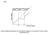
- Fig. 7 shows one example of an internal voltage vs. external voltage characteristic of a conventional internal voltage generating circuit.
- the internal voltage indicates such a constant voltage characteristic that when the external voltage ranges from 0 to a voltage VN (first voltage section or range), the external voltage is outputted as the internal voltage and when the external voltage ranges from the voltage VN to a boundary voltage VT (second voltage section or range), a constant voltage is outputted regardless of the external voltage.
- the internal voltage indicates such a variable voltage characteristic that a voltage is outputted which vertically rises at the final stage of the second voltage range and linearly rises from the voltage that has risen at the final stage of the second voltage range in a section or range (third voltage range) in which the external voltage becomes greater than or equal to the boundary voltage VT.
- a burn-in test for applying a source voltage higher than normal specifications to manufactured semiconductor devices so as to activate them under high temperatures is applied to each manufactured semiconductor device.
- the semiconductor device is activated in the third voltage range.
- the semiconductor device is activated in the second voltage range. Whether the semiconductor device should be activated in the second voltage range or the third voltage range, is controlled according to the level of an applied external voltage. Further, the switching between the voltage ranges is carried out by changing the level of the external voltage.
- the section or range of the internal voltage is not suitably set to either the second voltage range or the third voltage range and hence becomes unstable, thus resulting in the output of an unstable internal voltage from the internal voltage generating circuit
- the present invention provides an internal voltage generating circuit of the present invention for generating an internal voltage from an external voltage inputted thereto, which is characterized in that the internal voltage indicates such a constant voltage characteristic that the internal voltage is brought to a constant voltage regardless of the external voltage when the external voltage falls within a first voltage range, the internal voltage indicates such a variable voltage characteristic that when the external voltage falls within a second voltage range larger than the first voltage range, the internal voltage is brought to a variable voltage which is larger than the constant voltage and increases linearly with an increase in the external voltage, and a first boundary voltage for switching a characteristic of the internal voltage from the variable voltage characteristic to the constant voltage characteristic is lower than a second boundary voltage for switching the characteristic thereof from the constant voltage characteristic to the variable voltage characteristic.
- Another invention provides an internal voltage generating circuit comprising:
- a further invention provides an internal voltage generating circuit wherein the detecting means includes,
- a still further invention provides an internal voltage generating circuit wherein the voltage divider circuit is able to freely set the dependence of the voltage division ratio on temperature.
- a still further invention provides an internal voltage generating circuit wherein the voltage divider circuit includes,
- a still further invention provides an internal voltage generating circuit wherein the voltage division load circuit uses resistors as the load elements.
- a still further invention provides an internal voltage generating circuit wherein the voltage division load circuit is able to freely set the dependence of the voltage division ratio on temperature by forming the resistor of the external source-side load circuit and the resistor of the ground source-side load circuit from resistive materials of two types or more, which are different in temperature coefficient from each other.
- a still further invention provides an internal voltage generating circuit wherein the voltage division load circuit uses polysilicon and an n- or p-type silicon diffusion layer as the resistive materials.
- a still further invention provides an internal voltage generating circuit wherein the switch circuit has one or a plurality of short-circuit switch elements connected in parallel with the load elements to be short-circuited of the voltage division load circuit and is activated so as to bring the short-circuit switch elements into conduction or non-conduction in accordance with the determination signal.
- a still further invention provides an internal voltage generating circuit wherein the switch circuit uses a MOS transistor as the short-circuit switch element.
- a still further invention provides an internal voltage generating circuit wherein the voltage divider circuit further includes adjusting fuses for short-circuiting between the terminals of the predetermined load element of the load elements and is able to adjust the voltage division ratio of the voltage division load circuit by cutting out any of the adjusting fuses.
- a still further invention provides an internal voltage generating circuit wherein the comparing circuit includes,
- a still further invention provides an internal voltage generating circuit wherein the variable voltage generator has an output terminal connected to an input terminal of the output circuit and is activated so as to output the variable voltage to the output circuit when the determination signal is the second logical value and deactivated so as to stop the output of the variable voltage to the output circuit when the determination signal is the first logical value and
- variable voltage generator includes,
- a hysteresis characteristic is imparted to an internal voltage by switching a characteristic of an internal voltage from a constant voltage characteristic to a variable voltage characteristic when an external voltage is of a second boundary voltage and switching the characteristic of the internal voltage from the variable voltage characteristic to the constant voltage characteristic when the external voltage is of a first boundary voltage smaller than the second boundary voltage.
- An external voltage section or range for providing the constant voltage characteristic and an external voltage section or range for providing the variable voltage characteristic can be both enlarged as compared with the prior art.
- variations in first and second boundary voltages with respect to temperatures due to a variation in reference voltage with respect to the temperature can be corrected by freely setting the dependence of a voltage division ratio of a voltage divider circuit on the temperature.
- a voltage division ratio of a voltage division load circuit can be adjusted by opening or cutting out adjusting fuses so as to free short-circuiting of a predetermined load element.
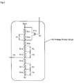
- Fig. 1 shows an internal voltage generating circuit according to a first embodiment of the present invention.
- the internal voltage generating circuit comprises a reference voltage generator 100, an amplifier circuit 110 which serves as a constant voltage generator, a voltage divider circuit 120, a comparing circuit 130, a burn-in voltage generator 150 which serves as a variable voltage generator, and an internal voltage output circuit 160.
- the reference voltage generator 100 is a circuit for generating a predetermined reference voltage VREF independent on an external voltage.
- the reference voltage VREF ranges from 1.3[V] to 1.4[V], for example.
- the amplifier circuit 110 includes a differential amplifier which is composed of an NMOS transistor N1 whose gate electrode is supplied with the reference voltage VREF, an NMOS transistor N2 whose source electrode is electrically connected to a source electrode of the NMOS transistor N1 and which forms a differential pair together with the NMOS transistor N1, an NMOS transistor N3 activated as a constant current source, which has gate and drain electrodes respectively electrically connected to the gate electrode of the NMOS transistor N1 and the source electrode of the NMOS transistor N1 and has a source electrode electrically grounded, a PMOS transistor P1 whose source and drain electrodes are respectively electrically connected to an external voltage VEXT and a drain electrode of the NMOS transistor N1, and a PMOS transistor P2 whose gate, drain and source electrodes are respectively electrically connected to the gate electrode of the NMOS transistor N1, a drain electrode of the NMOS transistor N2 and the external voltage VEXT, whose gate and drain electrodes are commonly connected to each other and which forms a load pair together
- the amplifier circuit 110 has a PMOS transistor P3 whose gate and source electrodes are respectively electrically connected to the drain electrode of the NMOS transistor N1 and the external voltage VEXT, a resistor R1 (corresponding to a first boost or set-up load element) provided between the drain electrode of the PMOS transistor P3 and a gate electrode of the NMOS transistor N2, and a resistor R2 (corresponding to a second set-up load element) provided between the gate electrode of the NMOS transistor N2 and a ground voltage.
- the voltage divider circuit 120 has a voltage division load circuit wherein resistors R4, R5 and R6 are connected in series in this order, one end of the resistor R4 is electrically connected to the external voltage VEXT, one end of the resistor R6 is electrically grounded and a point at which the resistors R5 and R6 are joined to each other, is used as a terminal for outputting a fractionally-divided voltage Va, whereby a fraction of the external voltage VEXT available is made by an external source-side load circuit composed of the resistors R4 and R5 and a ground source-side load circuit composed of the resistor R6, and a PMOS transistor P4 used as a switch circuit connected in parallel to the resistor R4 so as to short-circuit or open the resistor R4.
- the voltage divider circuit 120 makes a fraction of the external voltage VEXT in a voltage division ratio (first voltage division ratio) determined by the ratio between the total resistance value of the series-connected resistors R4 and R5 and the resistance value of the resistor R6.
- first voltage division ratio the voltage division ratio
- second voltage division ratio the voltage division ratio
- a voltage Va1 obtained by making the fraction of the external voltage VEXT in the first voltage division ratio becomes VEXT x R6/(R4 + R5 + R6) and a voltage Va2 obtained by making the fraction of the external voltage VEXT in the second voltage division ratio becomes VEXT x R6/(R5 + R6) .
- the comparing circuit 130 includes a comparator C1 having an inverse input terminal (-) supplied with the reference voltage VREF and a non-inverse input terminal (+) supplied with the voltage Va, and a drive circuit of a type wherein inverters I1, I2 and I3 are electrically connected in series and an output terminal of the inverter I3 is electrically connected to the gate electrode of the PMOS transistor P4 of the voltage divider circuit 120.
- the comparator C1 compares the level of the reference voltage VREF with that of the voltage Va. If Va ⁇ VREF, then the comparator C1 outputs an output voltage Vb of a logical level "Low" (hereinafter expressed as "L") therefrom.
- the comparator C1 If Va ⁇ VREF, then the comparator C1 outputs an output voltage Vb of a logical level "High” (hereinafter represented as “H") therefrom.
- the drive circuit outputs a determination or decision voltage Vc brought to "H” (corresponding to a first logical value) when Vb is of "L” and a decision voltage Vc brought to "L” (corresponding to a second logical value) when Vb is of "H”.
- the burn-in voltage generator 150 includes a PMOS transistor P5 whose gate electrode is supplied with the decision voltage Vc and whose source electrode is electrically connected to the external voltage VEXT, and a resistor R3 provided between a drain electrode of the PMOS transistor P5 and the output terminal INTN of the amplifier circuit 110. Further, the burn-in voltage generator 150 uses a terminal of the resistor R3 on the amplifier circuit 110 side as an output terminal INTB.
- the burn-in voltage generator 150 is activated so as to output a burn-in voltage (variable voltage) VINTB having a value larger than the constant voltage VINTN of the amplifier circuit 110 from the output terminal INTB.
- VINTB VEXT x (R1 + R2)/(R1 + R2 + R3) .
- the internal voltage output circuit 160 is of a circuit for supplying the constant voltage VINTN inputted from the amplifier circuit 110 or the burn-in voltage VINTB inputted from the burn-in voltage generator 150 to an internal circuit (not shown) as an internal voltage VINT.
- the voltage divider circuit 120 and the comparing circuit 130 constitute a detecting means.
- the detecting means detects that the external voltage VEXT has been boosted to the second boundary voltage VT2 or more, the detecting means changes the decision voltage Vc from “H” to "L".
- the detecting means senses that the external voltage VEXT has been reduced to the first boundary voltage VT1 or less, the detecting means changes the decision voltage Vc from "L" to "H".
- Fig. 2 is a diagram showing an input/output voltage characteristic of the internal voltage generating circuit shown in Fig. 1, i.e., an internal voltage VINT vs. external voltage VEXT characteristic.
- a second voltage range in which VEXTN ⁇ VEXT ⁇ VT1 upon a reduction in VEXT and VEXTN ⁇ VEXT ⁇ VT2 upon an increase in VEXT corresponds to a constant voltage characteristic zone or region in which the constant voltage VINTN is outputted regardless of the external voltage VEXT.
- a third voltage range in which VT1 ⁇ VEXT upon the reduction in VEXT and VT2 ⁇ VEXT upon the increase in VEXT corresponds to a variable voltage characteristic region in which the burn-in voltage VINTB (>VINTN) proportional to the external voltage VEXT is outputted.
- the boundary voltage VT2 at which a constant voltage characteristic is changed to a variable voltage characteristic with the increase in VEXT is different from the boundary voltage VT1 at which the variable voltage characteristic is changed to the constant voltage characteristic with the drop in VEXT.
- the internal voltage VINT has a hysteresis characteristic with respect to the external voltage VEXT (only the switching between the second voltage range and the third voltage range at the time of the increase in external voltage and the switching between the second voltage range and the third voltage range at the time of the decrease in external voltage are different from each other in the internal voltage generating circuit shown in Fig. 1).
- Fig. 2 also illustrates characteristics of the reference voltage VREF, the voltage Va and the output voltage Vb of the comparator C1 with respect to the external voltage VEXT simultaneously with the above characteristics.
- the PMOS transistor P5 of the burn-in voltage generator 150 is turned OFF and the PMOS transistor P3 of the amplifier circuit 110 is turned ON.
- the external voltage VEXT is outputted as the internal voltage VINT as it is through the PMOS transistor P3 and the internal voltage output circuit 160.
- the constant voltage VINTN is input to the internal voltage output circuit 160 from which VINTN is supplied to the internal circuit as the internal voltage VINT.
- the PMOS transistor P5 is turned ON to activate the burn-in voltage generator 150, whereby the switching from the second voltage range to the third voltage range is performed.
- the internal voltage output circuit 160 raises the internal voltage VINT and supplies the burn-in voltage VINTB to the internal circuit as VINT.
- the burn-in voltage VINTB is also applied to the output terminal INTN of the amplifier circuit 110 so that the voltage applied to the gate electrode of the NMOS transistor N2 is raised to increase the drain voltage of the NMOS transistor N1.
- the PMOS transistor P3 is turned OFF to deactivate the amplifier circuit 110.
- the PMOS transistor P4 is turned ON to short-circuit the resistor R4.
- Va1 to Va2 VEXT x R6/(R5 + R6) .
- the PMOS transistor P5 is turned OFF to deactivate the burn-in voltage generator 150, whereby the switching from the third voltage range to the second voltage range is performed.
- the PMOS transistor P3 is freed from the OFF state owing to the deactivation of the burn-in voltage generator 150 to thereby activate the amplifier circuit 110.
- the amplifier circuit 110 generates the constant voltage VINTN at the output terminal INTN thereof.
- the internal voltage output circuit 160 reduces the internal voltage VINT and supplies VINTN to the internal circuit as VINT.
- the PMOS transistor P4 is turned OFF to open the resistor R4, so that the fractionally-divided voltage Va is switched from Va2 to Va1.
- the external voltage changed from the third voltage range to the second voltage range is set lower than the external voltage changed from the second voltage range to the third voltage range so that the switching between the second voltage range and the third voltage range is provided with the hysteresis characteristic.
- the voltage division ratio of the voltage divider circuit 120 is changed to lower the external voltage point changed from the third voltage range to the second voltage range as compared with the external voltage point switched from the second voltage range to the third voltage range, thereby providing the switching between the second voltage range and the third voltage range with the hysteresis characteristic.
- the internal voltage which has first entered into the third voltage range from the second voltage range, is prevented from immediately returning to the second voltage range and the internal voltage, which has first entered into the second voltage range from the third voltage range, is prevented from immediately returning to the third voltage range.
- the internal voltage can be stably outputted.
- the second voltage range and the third voltage range can be both enlarged by the provided hysteresis characteristic as compared with the prior art.
- the configuration of the voltage divider circuit 120 is not necessarily limited to the above.
- the change of the voltage division ratio may be done by short-circuiting the resistor R5 with the PMOS transistor P2.
- the same operation as described above can be performed by separating the resistor R6 from others and opening/short-circuiting one of the separated resistors using an NMOS transistor.
- the load elements R4 through R6 are not necessarily limited to the resistors.
- diode-connected MOS transistors or the MOS transistors connected in series may be used in place of the resistor R5.
- the switch element P4 is not necessarily limited to the MOS transistor.
- any one may be used if capable of changing the voltage division ratio by forming the external source-side load circuit inserted between the external source or voltage and the fractionally-divided voltage output terminal and the ground source-side load circuit inserted between the ground source or voltage and the fractionally-divided voltage output terminal using three or more load elements and by opening/short-circuiting a predetermined load element with a switch element.
- a voltage divider circuit 140 shown in Fig. 3 may be used which is capable of adjusting the first voltage division ratio and the second voltage division ratio.
- series-connected resistors R11 through R15 form an external source-side load circuit
- series-connected resistors R16 through R18 constitute a source- side load circuit.
- a PMOS transistor P11 which serves as a switch element, is provided in parallel to a series resistor composed of the resistors R11 and R12. Further, adjusting fuses F1 through F5 cuttable by the irradiation of a laser beam or the like are respectively provided in parallel with the resistors R12, R14, R15, R17 and R18.
- the first and second voltage division ratios can be simultaneously adjusted by cutting out any of the adjusting fuses F2 through F5.
- the first voltage division ratio (corresponding to the voltage division ratio at the time that the transistor P11 is OFF) can be singly adjusted by cutting out or opening the fuse F1.
- the configuration of the burn-in voltage generator 150 is not necessarily limited to the above.
- the burn-in voltage generator 150 may be configured so that the PMOS transistor P5 corresponding to the switch element is provided between the resistor R3 and the output terminal INTB without being provided between the external voltage and the resistor R3 corresponding to the step-down load element.
- the burn-in voltage generator 150 may be configured so as to directly output the external voltage with the resistor R3 as 0[ ⁇ ].
- the burn-in voltage generator 150 is not necessarily limited to one shown in Fig. 1.
- the switch element is not limited to the PMOS transistor.
- the step-down load element is not limited to the resistor.
- diode-connected MOS transistors or the MOS transistors connected in series may be used as the step-down load element.
- the configuration of the amplifier circuit 110 is not necessarily limited to the above.
- the amplifier circuit 110 may be constructed such that a switch element brought into conduction when the decision voltage Vc is "H” and opened when the decision voltage Vc is "L”, is provided between the point of connection between the PMOS transistor P3 and the resistor R1 and the output terminal INTN without using the point of connection between the PMOS transistor P3 and the resistor R1 as the output terminal INTN.
- a reference voltage VREF has a dependence on the temperature where an internal voltage generating circuit is activated under a high temperature
- an external voltage point boundary voltage
- Fig. 4 is a diagram for describing a temperature-dependence of a boundary voltage at the time that VREF is dependent on the temperature and a fractionally-divided voltage Va (i.e., a voltage division ratio of a voltage divider circuit) is independent on the temperature.
- a fractionally-divided voltage Va i.e., a voltage division ratio of a voltage divider circuit
- the reference voltage depends on a negative temperature and the reference voltage is lowered to VREF2. Since the boundary voltage becomes VT4 by doing so, the voltage range is changed at an external voltage lower than a desired voltage value VT3.
- the reference voltage is dependent on a positive temperature and the reference voltage is raised to VREF3. Since the boundary voltage becomes VT5 in this case, the voltage range is changed at an external voltage higher than the desired voltage value VT3.
- the same as described above can be said of the internal voltage generating circuit shown in Fig. 1. It is basically desirable that the point (boundary voltage) of switching between the voltage ranges is not dependent on the temperature.
- the internal voltage generating circuit according to the second embodiment is characterized by imparting such a temperature characteristic as to correct variations in the first and second boundary voltages VT1 and VT2 with respect to temperature, to the fractionally-divided voltage Va corresponding to the output voltage of the voltage divider circuit 120 when the reference voltage VREF produced from the reference voltage generator 100 in the internal voltage generating circuit shown in Fig. 1 varies with temperature.
- the internal voltage generating circuit according to the second embodiment is characterized in that the above temperature characteristic is imparted to the fractionally-divided voltage Va by setting a temperature coefficient of the external source-side load circuit composed of the resistors R4 and R5 in the voltage divider circuit 120 shown in Fig. 1 and a temperature coefficient of the ground source-side load circuit composed of the resistor R6 in the voltage divider circuit 120 to different values respectively.
- resistive elements have positive temperature coefficients and are different from each other in temperature coefficient ranges settable according to the material.
- a temperature coefficient of an n-type or p-type diffusion layer (hereinafter called simply "diffusion layer") composed of silicon is normally larger than that of polysilicon.
- the temperature coefficients of the diffusion layer and the polysilicon can be respectively set within a predetermined range in accordance with an impurity concentration, a production process, etc. Therefore, the resistors R4 through R6 are formed using the diffusion layer or the polysilicon.
- the diffusion layer is used for the resistors R4 and R5 and the polysilicon is used for the resistor R6 so as to impart the negative temperature-dependence to the fractionally-divided voltage Va.
- the temperature coefficients of the resistors R5 and R6 are respectively set in such a manner that a variation in the voltage Va2 with respect to the temperature under a second voltage division ratio at the time that the external voltage is of the first boundary voltage VT1, becomes equal to the variation in VREF with respect to the temperature.
- the temperature coefficient of the resistor R4 is set such that a variation in fractionally-divided voltage Va1 with respect to the temperature under a first voltage division ratio at the time that the external voltage is of the second boundary voltage VT2, becomes equal to the variation in VREF with respect to the temperature .
- the temperature coefficient of the resistor R6 is smaller than the temperature coefficients of the resistors R4 and R5.
- the polysilicon is used for the resistors R4 and R5 and the diffusion layer is used for the resistor R6.
- the temperature coefficients of the resistors R4 through R6 are set such that the temperature variation in Va2 at the first boundary voltage VT1 and the temperature variation in Va1 at the second boundary voltage VT2 are respectively equal to the temperature variation in VREF.
- the temperature coefficient of the resistor R6 is larger than the temperature coefficients of the resistors R4 and R5.
- Fig. 5 is a diagram for describing the operation for correcting boundary voltages (corresponding to the first and second boundary voltages VT1 and VT2) with respect to temperature variations in the internal voltage generating circuit according to the second embodiment of the present invention.
- a reference voltage VREF at the time that the internal voltage generating circuit is activated under ordinary temperatures
- a boundary voltage (VT1 or VT2) at this time is defined as VT.
- the reference voltage VREF is dependent on a negative temperature and is lowered to VREF2 when the internal voltage generating circuit is activated under a high temperature. Since the voltage Va (Va1 or Va2) is set so as to have a positive temperature-dependence at this time, the characteristic of the voltage Va with respect to the external voltage changes from A to B in the drawing.
- the reference voltage VREF is dependent on the negative temperature and is increased to VREF3. Since the voltage Va (Va1 or Va2) is set so as to have a positive temperature-dependence at this time, the characteristic of the voltage Va with respect to the external voltage changes from A to C in the drawing. Thus, the boundary voltage is raised so as to be corrected to the same VT as when the internal voltage generating circuit is activated under ordinary temperatures.
- the respective resistors of the voltage divider circuit 120 are respectively formed of materials having different temperature coefficients.
- Table 1 shown below when the reference voltage VREF is dependent on the negative temperature, the temperature coefficient of the resistor R6 is set so as to be smaller than the temperature coefficients of the resistors R4 and R5, whereas when the reference voltage VREF is dependent on the positive temperature, the temperature coefficient of the resistor R6 is set so as to be larger than the temperature coefficients of the resistors R4 and R5. Further, such an output vs.
- a voltage divider circuit 120 shown in Fig. 6 is used as the above-described voltage divider circuit and the variations in the boundary voltage with respect to the temperature may be corrected in the following manner.
- series-connected resistors R21 through R23 constitute an external source-side load circuit and series-connected resistors R24 and R25 constitute a ground source-side load circuit.
- a PMOS transistor P21 which serves as a switch element, is provided in parallel with the resistor R21.
- Resistive materials having different temperature coefficients are respectively used for the resistors R22 and R23 and the resistors R24 and R25.
- the resistors R22 and R24 are respectively formed of a diffusion layer and the resistors R23 and R25 are respectively formed of polysilicon.
- a temperature characteristic of a fractionally-divided voltage Va2 at a second voltage division ratio can be controlled by adjusting the ratio between the resistance values of the resistors R22 and R23 and the ratio between the resistance values of the resistors R24 and R25, the degree of freedom of the control on the temperature characteristic of Va2 can be enlarged.
- an advantageous effect can be brought about in that since a hysteresis characteristic is imparted to an internal voltage by switching the characteristic of an internal voltage from a constant voltage characteristic to a variable voltage characteristic when an external voltage is of a second boundary voltage and switching the characteristic of the internal voltage from the variable voltage characteristic to the constant voltage characteristic when the external voltage is of a first boundary voltage smaller than the second boundary voltage, a stable internal voltage can be outputted even when the external voltage is unstable in the vicinity of a characteristic changeover.
- Another advantageous effect can be brought about in that an external voltage range brought to the constant voltage characteristic and an external voltage range brought to the variable voltage characteristic can be both enlarged as compared with the prior art.
- a further advantageous effect can be brought about in that variations in first and second boundary voltages with respect to the temperature due to a variation in reference voltage with respect to the temperature can be corrected by freely setting the dependence of a voltage division ratio of a voltage divider circuit on the temperature.
- a still further advantageous effect can be brought about in that a voltage division ratio of a voltage division load circuit can be adjusted by opening or cutting out adjusting fuses so as to free short-circuiting of predetermined load elements.
Landscapes
- Engineering & Computer Science (AREA)
- Microelectronics & Electronic Packaging (AREA)
- Physics & Mathematics (AREA)
- Automation & Control Theory (AREA)
- General Physics & Mathematics (AREA)
- Radar, Positioning & Navigation (AREA)
- Electromagnetism (AREA)
- Nonlinear Science (AREA)
- Continuous-Control Power Sources That Use Transistors (AREA)
- Dram (AREA)
- Semiconductor Integrated Circuits (AREA)
- Control Of Electrical Variables (AREA)
- Amplifiers (AREA)
Applications Claiming Priority (3)
| Application Number | Priority Date | Filing Date | Title |
|---|---|---|---|
| JP204369/96 | 1996-08-02 | ||
| JP20436996 | 1996-08-02 | ||
| JP20436996A JP3516556B2 (ja) | 1996-08-02 | 1996-08-02 | 内部電源回路 |
Publications (3)
| Publication Number | Publication Date |
|---|---|
| EP0822476A2 true EP0822476A2 (de) | 1998-02-04 |
| EP0822476A3 EP0822476A3 (de) | 1999-01-20 |
| EP0822476B1 EP0822476B1 (de) | 2003-06-04 |
Family
ID=16489381
Family Applications (1)
| Application Number | Title | Priority Date | Filing Date |
|---|---|---|---|
| EP97105238A Expired - Lifetime EP0822476B1 (de) | 1996-08-02 | 1997-03-27 | Interne Spannungserzeugungsschaltung |
Country Status (7)
| Country | Link |
|---|---|
| US (1) | US5856756A (de) |
| EP (1) | EP0822476B1 (de) |
| JP (1) | JP3516556B2 (de) |
| KR (1) | KR100331294B1 (de) |
| CN (1) | CN1141714C (de) |
| DE (1) | DE69722523T2 (de) |
| TW (1) | TW379324B (de) |
Cited By (2)
| Publication number | Priority date | Publication date | Assignee | Title |
|---|---|---|---|---|
| DE10361724A1 (de) * | 2003-12-30 | 2005-08-04 | Infineon Technologies Ag | Spannungsregelsystem |
| CN102436280A (zh) * | 2011-11-09 | 2012-05-02 | 福建星网锐捷网络有限公司 | 电压稳定输出装置和整机中的风扇转速控制系统及方法 |
Families Citing this family (55)
| Publication number | Priority date | Publication date | Assignee | Title |
|---|---|---|---|---|
| US6066979A (en) * | 1996-09-23 | 2000-05-23 | Eldec Corporation | Solid-state high voltage linear regulator circuit |
| JP3117128B2 (ja) * | 1997-01-31 | 2000-12-11 | 日本電気株式会社 | 基準電圧発生回路 |
| JPH10260741A (ja) * | 1997-03-17 | 1998-09-29 | Oki Electric Ind Co Ltd | 定電圧発生回路 |
| US5942809A (en) * | 1997-12-24 | 1999-08-24 | Oki Electric Industry Co., Ltd. | Method and apparatus for generating internal supply voltage |
| KR100451421B1 (ko) * | 1997-12-29 | 2004-12-17 | 주식회사 하이닉스반도체 | 전원 전압 레귤레이션 회로 |
| US6091287A (en) * | 1998-01-23 | 2000-07-18 | Motorola, Inc. | Voltage regulator with automatic accelerated aging circuit |
| KR100735440B1 (ko) * | 1998-02-13 | 2007-10-24 | 로무 가부시키가이샤 | 반도체장치 및 자기디스크장치 |
| JPH11231954A (ja) * | 1998-02-16 | 1999-08-27 | Mitsubishi Electric Corp | 内部電源電圧発生回路 |
| JP3512332B2 (ja) * | 1998-04-07 | 2004-03-29 | 富士通株式会社 | 内部電圧発生回路 |
| DE19832309C1 (de) * | 1998-07-17 | 1999-10-14 | Siemens Ag | Integrierte Schaltung mit einem Spannungsregler |
| JP2000040394A (ja) * | 1998-07-21 | 2000-02-08 | Fujitsu Ltd | 半導体装置 |
| JP3278635B2 (ja) * | 1999-05-27 | 2002-04-30 | 沖電気工業株式会社 | 半導体集積回路 |
| JP3262103B2 (ja) * | 1999-06-07 | 2002-03-04 | 日本電気株式会社 | 内部電源回路を有する半導体装置 |
| US6380791B1 (en) * | 2000-05-16 | 2002-04-30 | National Semiconductor Corporation | Circuit including segmented switch array for capacitive loading reduction |
| JP2002008374A (ja) * | 2000-06-22 | 2002-01-11 | Mitsubishi Electric Corp | 電圧降圧回路 |
| US6377108B1 (en) * | 2000-08-28 | 2002-04-23 | Intel Corporation | Low jitter differential amplifier with negative hysteresis |
| US6456139B1 (en) * | 2000-10-20 | 2002-09-24 | Sun Microsystems, Inc. | Auto-detection and auto-enable of compact PCI bus pull-ups |
| DE10055242C1 (de) * | 2000-11-08 | 2002-02-21 | Infineon Technologies Ag | Schaltungsanordnung mit interner Versorgungsspannung |
| US6665843B2 (en) * | 2001-01-20 | 2003-12-16 | International Business Machines Corporation | Method and system for quantifying the integrity of an on-chip power supply network |
| JP3868756B2 (ja) * | 2001-04-10 | 2007-01-17 | シャープ株式会社 | 半導体装置の内部電源電圧発生回路 |
| US6750683B2 (en) * | 2001-04-30 | 2004-06-15 | Stmicroelectronics, Inc. | Power supply detection circuitry and method |
| JP3494635B2 (ja) * | 2001-09-19 | 2004-02-09 | 沖電気工業株式会社 | 内部降圧電源回路 |
| JP3825300B2 (ja) * | 2001-10-31 | 2006-09-27 | Necエレクトロニクス株式会社 | 内部降圧回路 |
| US6815998B1 (en) * | 2002-10-22 | 2004-11-09 | Xilinx, Inc. | Adjustable-ratio global read-back voltage generator |
| US20040124909A1 (en) * | 2002-12-31 | 2004-07-01 | Haider Nazar Syed | Arrangements providing safe component biasing |
| JP3561716B1 (ja) | 2003-05-30 | 2004-09-02 | 沖電気工業株式会社 | 定電圧回路 |
| US20050088239A1 (en) * | 2003-10-23 | 2005-04-28 | Tai Jy-Der D. | Short-circuit detecting and protecting circuit for integrated circuit |
| US7042280B1 (en) * | 2003-12-15 | 2006-05-09 | National Semiconductor Corporation | Over-current protection circuit |
| JP4033472B2 (ja) * | 2004-02-23 | 2008-01-16 | ローム株式会社 | 電圧検出回路及びそれを用いたバッテリ装置 |
| US7057447B1 (en) * | 2004-03-04 | 2006-06-06 | National Semiconductor Corporation | Voltage regulator using a single voltage source and method |
| JP4791700B2 (ja) * | 2004-03-29 | 2011-10-12 | 株式会社リコー | 半導体装置、半導体装置の調整方法および電子装置 |
| US7420397B2 (en) * | 2004-06-02 | 2008-09-02 | Stmicroelectronics Sa | Low-consumption inhibit circuit with hysteresis |
| JP4473669B2 (ja) * | 2004-07-28 | 2010-06-02 | 株式会社リコー | 定電圧回路、その定電圧回路を使用した定電流源、増幅器及び電源回路 |
| KR100596977B1 (ko) * | 2004-08-20 | 2006-07-05 | 삼성전자주식회사 | 외부 기준 전압과 내부 기준 전압을 동시에 이용하는 기준전압 발생 회로 및 이를 이용한 기준 전압 발생 방법 |
| KR101056737B1 (ko) | 2004-09-20 | 2011-08-16 | 삼성전자주식회사 | 내부 전원 전압을 발생하는 장치 |
| US7248102B2 (en) * | 2005-01-20 | 2007-07-24 | Infineon Technologies Ag | Internal reference voltage generation for integrated circuit testing |
| US20080048746A1 (en) * | 2006-08-25 | 2008-02-28 | Microchip Technology Incorporated | Hysteresis Comparator with Programmable Hysteresis Width |
| JP2008123586A (ja) * | 2006-11-09 | 2008-05-29 | Toshiba Corp | 半導体装置 |
| KR100803363B1 (ko) | 2006-11-13 | 2008-02-13 | 주식회사 하이닉스반도체 | 반도체 메모리 장치의 전압 생성 회로 |
| JP4938439B2 (ja) * | 2006-12-27 | 2012-05-23 | オンセミコンダクター・トレーディング・リミテッド | スイッチング制御回路 |
| JP5104118B2 (ja) * | 2007-08-09 | 2012-12-19 | 富士通セミコンダクター株式会社 | 内部電源回路 |
| JP5085233B2 (ja) * | 2007-08-28 | 2012-11-28 | ルネサスエレクトロニクス株式会社 | 基準電圧発生回路及びタイマ回路 |
| US8436659B1 (en) * | 2008-06-24 | 2013-05-07 | Marvell International Ltd. | Circuits and methods for reducing electrical stress on a transistor |
| JP2010097344A (ja) * | 2008-10-15 | 2010-04-30 | Elpida Memory Inc | 半導体装置 |
| KR101450255B1 (ko) * | 2008-10-22 | 2014-10-13 | 삼성전자주식회사 | 반도체 메모리 장치의 내부 전원 전압 발생 회로 |
| CN101739052B (zh) * | 2009-11-26 | 2012-01-18 | 四川和芯微电子股份有限公司 | 一种与电源无关的电流参考源 |
| CN102193572A (zh) * | 2010-03-11 | 2011-09-21 | 株式会社理光 | 基准电压产生电路 |
| KR101143446B1 (ko) | 2010-05-31 | 2012-05-22 | 에스케이하이닉스 주식회사 | 전압 발생 회로 |
| JP5514142B2 (ja) * | 2011-04-11 | 2014-06-04 | 株式会社東芝 | 受信回路 |
| KR20140079046A (ko) * | 2012-12-18 | 2014-06-26 | 에스케이하이닉스 주식회사 | 차동 증폭 회로 |
| KR102113717B1 (ko) * | 2013-12-30 | 2020-05-21 | 에스케이하이닉스 주식회사 | 반도체 장치 |
| CN108139445B (zh) * | 2015-10-05 | 2023-07-14 | 株式会社村田制作所 | 余量测定装置、电池组、电动工具、电动式飞机、电动车辆以及电源装置 |
| CN106292827B (zh) * | 2016-08-18 | 2018-09-21 | 华为技术有限公司 | 一种电压产生装置及半导体芯片 |
| JP6522201B1 (ja) * | 2018-05-14 | 2019-05-29 | ウィンボンド エレクトロニクス コーポレーション | 半導体装置 |
| CN109658957B (zh) * | 2019-03-07 | 2021-04-30 | 中国科学院微电子研究所 | 一种应用于三维存储器的稳压器电路及三维存储器 |
Citations (4)
| Publication number | Priority date | Publication date | Assignee | Title |
|---|---|---|---|---|
| US5184031A (en) * | 1990-02-08 | 1993-02-02 | Kabushiki Kaisha Toshiba | Semiconductor integrated circuit |
| JPH0696596A (ja) * | 1992-05-21 | 1994-04-08 | Samsung Electron Co Ltd | 半導体装置の内部電源発生回路 |
| EP0613071A2 (de) * | 1993-02-26 | 1994-08-31 | Nec Corporation | Integrierte Halbleiterschaltungsanordnung mit Spannungsüberwachungsschaltung mit geringem Energieverbrauch für eingebauten Abwärtsspannungsgenerator |
| US5510749A (en) * | 1992-01-28 | 1996-04-23 | Mitsubishi Denki Kabushiki Kaisha | Circuitry and method for clamping a boost signal |
Family Cites Families (3)
| Publication number | Priority date | Publication date | Assignee | Title |
|---|---|---|---|---|
| KR940008286B1 (ko) * | 1991-08-19 | 1994-09-09 | 삼성전자 주식회사 | 내부전원발생회로 |
| KR950004858B1 (ko) * | 1992-03-17 | 1995-05-15 | 삼성전자 주식회사 | 내부전원전압 발생회로 |
| KR950008453B1 (ko) * | 1992-03-31 | 1995-07-31 | 삼성전자주식회사 | 내부전원전압 발생회로 |
-
1996
- 1996-08-02 JP JP20436996A patent/JP3516556B2/ja not_active Expired - Fee Related
-
1997
- 1997-03-24 TW TW086103719A patent/TW379324B/zh not_active IP Right Cessation
- 1997-03-27 DE DE69722523T patent/DE69722523T2/de not_active Expired - Lifetime
- 1997-03-27 EP EP97105238A patent/EP0822476B1/de not_active Expired - Lifetime
- 1997-03-28 US US08/829,547 patent/US5856756A/en not_active Expired - Lifetime
- 1997-05-12 KR KR1019970018338A patent/KR100331294B1/ko not_active IP Right Cessation
- 1997-07-31 CN CNB971161186A patent/CN1141714C/zh not_active Expired - Fee Related
Patent Citations (4)
| Publication number | Priority date | Publication date | Assignee | Title |
|---|---|---|---|---|
| US5184031A (en) * | 1990-02-08 | 1993-02-02 | Kabushiki Kaisha Toshiba | Semiconductor integrated circuit |
| US5510749A (en) * | 1992-01-28 | 1996-04-23 | Mitsubishi Denki Kabushiki Kaisha | Circuitry and method for clamping a boost signal |
| JPH0696596A (ja) * | 1992-05-21 | 1994-04-08 | Samsung Electron Co Ltd | 半導体装置の内部電源発生回路 |
| EP0613071A2 (de) * | 1993-02-26 | 1994-08-31 | Nec Corporation | Integrierte Halbleiterschaltungsanordnung mit Spannungsüberwachungsschaltung mit geringem Energieverbrauch für eingebauten Abwärtsspannungsgenerator |
Non-Patent Citations (1)
| Title |
|---|
| PATENT ABSTRACTS OF JAPAN vol. 098, no. 007, 31 March 1998 & JP 06 096596 A (SAMSUNG ELECTRON CO LTD), 8 April 1994 * |
Cited By (4)
| Publication number | Priority date | Publication date | Assignee | Title |
|---|---|---|---|---|
| DE10361724A1 (de) * | 2003-12-30 | 2005-08-04 | Infineon Technologies Ag | Spannungsregelsystem |
| US7965066B2 (en) | 2003-12-30 | 2011-06-21 | Qimonda Ag | Voltage regulation system |
| CN102436280A (zh) * | 2011-11-09 | 2012-05-02 | 福建星网锐捷网络有限公司 | 电压稳定输出装置和整机中的风扇转速控制系统及方法 |
| CN102436280B (zh) * | 2011-11-09 | 2013-11-20 | 福建星网锐捷网络有限公司 | 电压稳定输出装置和整机中的风扇转速控制系统及方法 |
Also Published As
| Publication number | Publication date |
|---|---|
| EP0822476A3 (de) | 1999-01-20 |
| DE69722523T2 (de) | 2004-05-06 |
| JP3516556B2 (ja) | 2004-04-05 |
| CN1141714C (zh) | 2004-03-10 |
| EP0822476B1 (de) | 2003-06-04 |
| KR100331294B1 (ko) | 2002-06-20 |
| KR19980018101A (ko) | 1998-06-05 |
| DE69722523D1 (de) | 2003-07-10 |
| CN1176465A (zh) | 1998-03-18 |
| JPH1049243A (ja) | 1998-02-20 |
| TW379324B (en) | 2000-01-11 |
| US5856756A (en) | 1999-01-05 |
Similar Documents
| Publication | Publication Date | Title |
|---|---|---|
| US5856756A (en) | Internal voltage generating circuit | |
| US9746870B2 (en) | Semiconductor device including a constant voltage generation unit | |
| US6946821B2 (en) | Voltage regulator with enhanced stability | |
| EP0039215B1 (de) | Generatorschaltung einer Temperaturkompensationsspannung | |
| US4779037A (en) | Dual input low dropout voltage regulator | |
| JP4937865B2 (ja) | 定電圧回路 | |
| US8450986B2 (en) | Voltage regulator | |
| JP3851791B2 (ja) | 半導体集積回路 | |
| US5877617A (en) | Load current supply circuit having current sensing function | |
| US7834680B2 (en) | Internal voltage generation circuit for generating stable internal voltages withstanding varying external conditions | |
| JPH08508600A (ja) | Mosトランジスタの閾値電圧を調整する装置および方法 | |
| US7254080B2 (en) | Fuse circuit and electronic circuit | |
| US7109761B2 (en) | Comparator circuit | |
| US6091287A (en) | Voltage regulator with automatic accelerated aging circuit | |
| JP4175862B2 (ja) | 電圧設定回路及びその設定方法、並びに電圧検出回路及び定電圧発生回路 | |
| US6954058B2 (en) | Constant current supply device | |
| US20010005161A1 (en) | Level-shifting reference voltage source circuits and methods | |
| US7034605B2 (en) | Internal step-down power supply circuit | |
| EP0948762B1 (de) | Spannungsreglerschaltungen und halbleiterschaltung | |
| KR20020013800A (ko) | 데이터 처리 유닛용 주파수 판정 회로 | |
| US6559628B2 (en) | High voltage regulation circuit | |
| US7049833B2 (en) | Method for optimizing the accuracy of an electronic circuit | |
| JP3868131B2 (ja) | バックバイアス回路 | |
| US7183865B2 (en) | Oscillator circuit operating with a variable driving voltage | |
| US11566950B2 (en) | Process and temperature tracking reference load and method thereof |
Legal Events
| Date | Code | Title | Description |
|---|---|---|---|
| PUAI | Public reference made under article 153(3) epc to a published international application that has entered the european phase |
Free format text: ORIGINAL CODE: 0009012 |
|
| AK | Designated contracting states |
Kind code of ref document: A2 Designated state(s): DE FR NL |
|
| PUAL | Search report despatched |
Free format text: ORIGINAL CODE: 0009013 |
|
| AK | Designated contracting states |
Kind code of ref document: A3 Designated state(s): DE FR NL |
|
| AKX | Designation fees paid |
Free format text: DE FR NL |
|
| 17P | Request for examination filed |
Effective date: 19990720 |
|
| 17Q | First examination report despatched |
Effective date: 20011227 |
|
| GRAH | Despatch of communication of intention to grant a patent |
Free format text: ORIGINAL CODE: EPIDOS IGRA |
|
| GRAH | Despatch of communication of intention to grant a patent |
Free format text: ORIGINAL CODE: EPIDOS IGRA |
|
| GRAA | (expected) grant |
Free format text: ORIGINAL CODE: 0009210 |
|
| AK | Designated contracting states |
Designated state(s): DE FR NL |
|
| REF | Corresponds to: |
Ref document number: 69722523 Country of ref document: DE Date of ref document: 20030710 Kind code of ref document: P |
|
| ET | Fr: translation filed | ||
| PLBE | No opposition filed within time limit |
Free format text: ORIGINAL CODE: 0009261 |
|
| STAA | Information on the status of an ep patent application or granted ep patent |
Free format text: STATUS: NO OPPOSITION FILED WITHIN TIME LIMIT |
|
| 26N | No opposition filed |
Effective date: 20040305 |
|
| REG | Reference to a national code |
Ref country code: FR Ref legal event code: TP |
|
| PGFP | Annual fee paid to national office [announced via postgrant information from national office to epo] |
Ref country code: FR Payment date: 20120319 Year of fee payment: 16 |
|
| PGFP | Annual fee paid to national office [announced via postgrant information from national office to epo] |
Ref country code: NL Payment date: 20120322 Year of fee payment: 16 Ref country code: DE Payment date: 20120411 Year of fee payment: 16 |
|
| REG | Reference to a national code |
Ref country code: NL Ref legal event code: V1 Effective date: 20131001 |
|
| REG | Reference to a national code |
Ref country code: FR Ref legal event code: ST Effective date: 20131129 |
|
| REG | Reference to a national code |
Ref country code: DE Ref legal event code: R119 Ref document number: 69722523 Country of ref document: DE Effective date: 20131001 |
|
| PG25 | Lapsed in a contracting state [announced via postgrant information from national office to epo] |
Ref country code: DE Free format text: LAPSE BECAUSE OF NON-PAYMENT OF DUE FEES Effective date: 20131001 Ref country code: FR Free format text: LAPSE BECAUSE OF NON-PAYMENT OF DUE FEES Effective date: 20130402 |
|
| PG25 | Lapsed in a contracting state [announced via postgrant information from national office to epo] |
Ref country code: NL Free format text: LAPSE BECAUSE OF NON-PAYMENT OF DUE FEES Effective date: 20131001 |