US6954058B2 - Constant current supply device - Google Patents
Constant current supply device Download PDFInfo
- Publication number
- US6954058B2 US6954058B2 US10/795,323 US79532304A US6954058B2 US 6954058 B2 US6954058 B2 US 6954058B2 US 79532304 A US79532304 A US 79532304A US 6954058 B2 US6954058 B2 US 6954058B2
- Authority
- US
- United States
- Prior art keywords
- transistor
- current
- constant current
- circuit
- resistor
- Prior art date
- Legal status (The legal status is an assumption and is not a legal conclusion. Google has not performed a legal analysis and makes no representation as to the accuracy of the status listed.)
- Expired - Lifetime, expires
Links
Images
Classifications
-
- G—PHYSICS
- G05—CONTROLLING; REGULATING
- G05F—SYSTEMS FOR REGULATING ELECTRIC OR MAGNETIC VARIABLES
- G05F3/00—Non-retroactive systems for regulating electric variables by using an uncontrolled element, or an uncontrolled combination of elements, such element or such combination having self-regulating properties
- G05F3/02—Regulating voltage or current
- G05F3/08—Regulating voltage or current wherein the variable is DC
- G05F3/10—Regulating voltage or current wherein the variable is DC using uncontrolled devices with non-linear characteristics
- G05F3/16—Regulating voltage or current wherein the variable is DC using uncontrolled devices with non-linear characteristics being semiconductor devices
- G05F3/20—Regulating voltage or current wherein the variable is DC using uncontrolled devices with non-linear characteristics being semiconductor devices using diode- transistor combinations
- G05F3/26—Current mirrors
- G05F3/267—Current mirrors using both bipolar and field-effect technology
Definitions
- the present invention relates to a constant current supply device for controlling a current flowing through a main transistor to a constant value.
- the present invention also relates to a constant current supply device having a plurality of constant current output circuits.
- a constant current circuit disclosed in JP-A-5-35352 has an emitter-follower transistor for generating an output current and a parallel circuit connected to the emitter of the transistor.
- the parallel circuit comprises a diode and a resistor having a positive temperature coefficient.
- a current source circuit disclosed in JP-A-2000-124743 has a current mirror constant current circuit serving as a first constant current source circuit as well as second and third constant current source circuits connected between a power supply line and transistors forming the current mirror constant current circuit.
- a resistor having a negative temperature coefficient is connected between the power supply line and each of transistors composing the second and third constant current source circuits.
- a constant current circuit disclosed in JP-A-2002-236521 has a voltage generation circuit and a constant current supply device.
- the voltage generation circuit has a reference voltage circuit and a temperature characteristic correction circuit connected to the reference voltage circuit as a circuit for correcting the temperature characteristic of the reference voltage circuit.
- the constant current supply device is a circuit for controlling a current, which is generated by a voltage output by the reference voltage circuit with its temperature characteristic corrected as a current flowing through an internal current detection resistor.
- the internal current detection resistor has the temperature characteristic opposite to the temperature characteristic of the reference voltage circuit employed in the voltage generation circuit.
- a circuit shown in FIG. 12 is proposed as another constant current supply device 1 .
- the constant current supply device 1 controls a main current IL flowing through a main current path 4 to a constant magnitude.
- the main current path 4 is a path starting from a terminal 2 , passing through a resistor R 1 for detecting a current flowing through the resistor R 1 , a MOS transistor Q 1 and a resistor R 2 , and ending at a terminal 3 .
- a voltage appearing between the two ends of the resistor R 1 varies in accordance with the main current IL, changing a current flowing through the collector of a transistor Q 3 in a current mirror circuit 5 , which comprises a transistor Q 2 , the transistor Q 3 and resistors R 1 , R 2 and R 3 .
- a transistor Q 4 is connected between the collector of the transistor Q 3 and a power supply line 6 linked to a terminal 3 .
- the transistor Q 4 and a transistor Q 5 form a current mirror circuit 7 .
- a self-bias constant current circuit 9 using a voltage appearing between the base and the emitter as a reference voltage is connected between the transistor Q 2 and the power supply line 6 .
- a self-bias constant current circuit 10 using a voltage appearing between the base and the emitter as a reference voltage is connected between the transistor Q 5 and a power supply line 8 .
- this constant current supply device 1 when the main current IL exceeds a target current magnitude, for example, the voltage appearing between the two ends of the resistor R 1 also exceeds a predetermined level, increasing a voltage appearing between the base and emitter of the transistor Q 3 . Thus, a current flowing through the collector of the transistor Q 3 also rises as well. As a result, the electric potential appearing at the gate of the transistor Q 1 decreases, causing feedback control to operate to result in a decrease in the main current IL.
- a target current magnitude for example, the voltage appearing between the two ends of the resistor R 1 also exceeds a predetermined level, increasing a voltage appearing between the base and emitter of the transistor Q 3 .
- a current flowing through the collector of the transistor Q 3 also rises as well.
- the electric potential appearing at the gate of the transistor Q 1 decreases, causing feedback control to operate to result in a decrease in the main current IL.
- a current output by the circuit is detected as a voltage appearing between the two ends of a resistor, and changes of the detected voltage are fed back as changes of a voltage appearing between the base and emitter of a transistor.
- This constant current is generated on the basis of a reference voltage generated by a reference voltage generation circuit.
- a reference voltage generation circuit disclosed in JP-A-2000-112548 generates a high precision reference output voltage slightly lower than the electric potential of the power supply by fine adjustment of the resistance of a resistor device in a laser trimming process.
- trimming adjustment of a resistor can be carried out to optimize the temperature characteristic of the reference voltage.
- an IC 201 comprising a plurality of constant current output circuits 202 has also been proposed.
- the constant current output circuits 202 each operate by receiving a battery voltage VMAIN supplied by power supply lines 203 and 204 .
- the IC 201 outputs a constant current to every load RL connected to one of terminals 205 of the IC 201 .
- Each of the constant current output circuits 202 comprises transistors Q 201 to Q 205 , resistors R 201 to R 205 as well as constant current circuits 206 and 207 .
- the resistor R 201 is a current detection resistor and the transistor Q 203 is an output transistor.
- the temperature coefficient of the resistor R 201 is about equal to that of the transistor Q 203 .
- changes in current which are caused by changes in temperature, are compensated for to a certain degree.
- coordinated current adjustment needs to be performed by carrying out adjustment works such as a laser trimming process for the resistor R 204 and a trimming process for the transistors Q 201 and Q 202 for every constant current output circuit 202 .
- a controlled current which is a main current subjected to constant current control, flows through a main current path starting from a current output terminal, passing through a resistor for current detection as well as a main transistor and ending at a first power supply line.
- the main current is detected as a voltage appearing between the two ends of the resistor for current detection. This voltage is applied between the base and emitter of a second transistor employed in a first current mirror circuit. A current flowing through the second transistor flows into a second current mirror circuit.
- An electric potential appearing at the base of the main transistor is determined on the basis of a current output by the second current mirror circuit and a current output by a second constant current circuit.
- the main current exceeds a target current magnitude, for example, the voltage appearing between the two ends of the resistor for current detection, that is, the voltage applied between the base and emitter of the second transistor, also increases, tending to raise the current flowing through the collector of the second transistor and, hence, a current output by the second current mirror circuit.
- the constant current supply device exhibits an effect of reducing the electric potential appearing at the base of the main transistor and the main current.
- the main current is controlled to a constant value.
- the first constant current circuit works by taking a voltage appearing between the base and emitter of a transistor as a reference voltage. Thus, when the temperature increases, the output current generated by the first constant current circuit decreases in accordance with a temperature coefficient of ⁇ 2 mV/degrees Celsius for the voltage appearing between the base and the emitter. Since the first constant current circuit is a circuit for supplying a reference bias current to the first transistor, the decrease in output current reduces a current output by the second current mirror circuit. Thus, the electric potential appearing at the base of the main transistor increases. As a result, the main current rises, exceeding the target current magnitude.
- a first compensation resistor having a positive temperature coefficient is provided between a first power supply line and the emitter of a third transistor through which the current flowing through the collector of a second transistor flows.
- This configuration suppresses decreases of a voltage appearing between the base and emitter of a third transistor, decreases of a voltage appearing between the base and emitter of a fourth transistor and, hence, decreases of a current output by the second current mirror circuit.
- changes of the electric potential appearing at the base of the main transistor can be suppressed even when the temperature changes so that the main current can be controlled to a value equal to the target current magnitude.
- the current flowing through the third transistor serving as an output transistor is converted into a voltage appearing between the two ends of a current detection resistor connected in series to the third transistor.
- a predetermined target current magnitude for example, a voltage appearing between the base and emitter of the second transistor, hence, the current flowing through the collector of the second transistor.
- the output current adjustment circuit has a fourth transistor, through which a portion of a feedback current flows, for each of the constant current output circuits.
- the feedback current is a current flowing through the second transistor.
- the currents flowing through the fourth transistors of the constant current output circuits are controlled as a common single quantity in an aggregated manner instead of changing the currents individually.
- the aggregated current adjustment can be carried out with ease for the constant current output circuits and the time it takes to adjust the currents can also be shortened.
- components such as a trimming resistor are not needed for each of the constant current output circuits.
- the first to fourth transistors can each be a bipolar transistor or a FET or implemented as a bipolar circuit, a CMOS circuit, a BiCMOS circuit or the like.
- the above portion of a current flowing through the second transistor can be obtained by splitting the current flowing into the second transistor at the stage before the current flows into the second transistor or at the stage after the current flows out from the second transistor.
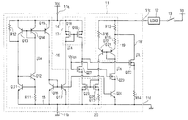
- FIG. 1 is an electric circuit diagram showing a constant current supply device implemented by a first embodiment of the present invention
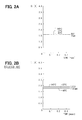
- FIGS. 2A and 2B are diagrams showing simulation waveforms of a main current for a case in which junction temperatures of transistors are changed;
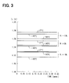
- FIG. 3 is a diagram showing simulation waveforms of the main current for a case in which resistances are changed by +10% or ⁇ 10%;
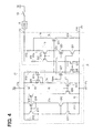
- FIG. 4 is an electric circuit diagram showing a constant current supply device implemented by a second embodiment of the present invention.
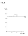
- FIG. 5 is a diagram showing a simulation waveform of a main current for the second embodiment
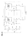
- FIG. 6 is an electric circuit diagram showing a constant current supply device implemented by a third embodiment of the present invention.
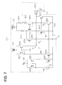
- FIG. 7 is a detailed electric circuit diagram showing a constant current output circuit
- FIG. 8 is a diagram showing a simulation result of an output current for a case in which resistances are increased by 10%
- FIG. 9 is a diagram showing a post trimming simulation result of an output current as a result obtained by trimming only a resistor
- FIG. 10 is a diagram showing a post trimming simulation result of an output current as a result obtained by trimming an emitter area ratio
- FIG. 11 is an electric circuit diagram showing a constant current supply device implemented by a fourth embodiment of the present invention.
- FIG. 12 is an electric circuit diagram showing a constant current supply device according to one related art.
- FIG. 13 is an electric circuit diagram showing a constant current supply device according to another related art.
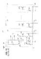
- a constant current supply device 11 shown in FIG. 1 is an integrated circuit (IC) used typically for driving an airbag of an automobile.
- Terminals 11 a and 11 b of the IC 11 are each a power supply terminal.
- a power supply voltage Vcc of typically 25V is applied between the terminals 11 a and 11 b .
- a terminal 11 c of the IC 11 is a current output terminal connected to one end of a load 12 , the other end of which is connected to a voltage boosting power supply through a high-side switch circuit 13 .
- the voltage boosting power supply is for supplying a power supply voltage of typically 35V to the load 12 by way of the high-side switch circuit 13 .
- the load 12 is a load to be borne in driving the airbag.
- the high-side switch circuit 13 is a semiconductor switching device.
- a terminal 11 d of the IC 11 is the ground terminal of a power system supplying power to the terminal 11 c .
- the constant current supply device 11 controls a current, which is flowing to the load 12 when the high-side switch circuit 13 is closed, to a constant magnitude of typically 1.5 A.
- a self-bias constant current circuit 16 for generating a constant current Ia is connected between a power supply line 14 (second power supply line) wired to the terminal 11 a and a power supply line 15 (first power supply line) linked to the terminals 11 b and 11 d .
- the constant current circuit 16 uses a voltage appearing between the base and emitter of a NPN-type transistor Q 11 as a reference voltage.
- Transistors composing the constant current circuit 16 are all bipolar transistors.
- a resistor R 11 is connected between the base and emitter of the transistor Q 11 as a resistor for determining a current magnitude.
- the base and collector of the transistor Q 11 are connected respectively to the emitter and base of a transistor Q 12 .
- a current mirror circuit comprising transistors Q 13 and Q 14 is connected between the power supply line 14 and the collectors of the transistors Q 11 and Q 12 .
- a resistor R 12 is connected between the emitter and collector of the transistor Q 13 as a resistor for activation.
- Transistors Q 15 and Q 16 are connected to each other in series between the power supply lines 14 and 15 .
- One of these transistors, i.e., the transistor Q 15 forms a current mirror circuit in conjunction with a transistor Q 14 .
- the transistor Q 16 forms a current mirror circuit in conjunction with a transistor Q 17 .
- a current mirror circuit 17 receives the constant current Ia generated by the constant current circuit 16 and outputs the constant current Ia as it is.
- the current mirror circuit 17 comprises MOS transistors Q 18 and Q 19 , the sources of which are connected to the power supply line 14 .
- the constant current circuit 16 and the current mirror circuit 17 form a second constant current circuit.
- a resistor R 13 current detection resistor
- an N-channel LDMOS transistor Q 20 main transistor
- a resistor R 14 feedback resistor
- a current mirror circuit 19 is a circuit inputting a constant bias current (reference current) serving as a reference and outputting a current corresponding to the reference current and the main current IL flowing through the resistor R 13 .
- the reference current is equal to the constant current Ia output from the constant current circuit 16
- the current mirror circuit 19 functions as a current detection device for outputting a current varying in accordance with changes in main current IL.
- the current mirror circuit 19 comprises PNP-type transistors Q 21 and Q 12 (first and second transistors respectively), a resistor R 15 (first resistor) and a resistor R 16 (second resistor).
- the bases of the transistors Q 21 and Q 12 are connected to each other.
- the resistor R 15 is connected between the emitter of the transistor Q 21 and the resistor R 13 .
- the resistor R 16 is connected between the emitter of the transistor Q 22 and the terminal 11 c .
- the resistors R 13 , R 15 and R 16 are each an aluminum wire resistor, the chip area occupied by each of the resistors can be reduced.
- the base and collector of the transistor Q 2 are connected to each other.
- a MOS transistor Q 23 and a NPN-type transistor Q 24 are connected in series between the collector of the transistor Q 21 and the power supply line 15 .
- the base of one of the transistors, i.e., the transistor Q 24 is connected to the bases of the transistors Q 16 and Q 17 , which are employed in the constant current circuit (the first constant current circuit) flowing the constant current Ia.
- the MOS transistor Q 23 has a function to fix an electric potential appearing at the collector of the transistor Q 24 .
- a bias voltage Vbias is supplied to the gate of the transistor Q 23 .
- a MOS transistor Q 25 (third transistor) and a resistor R 17 (first compensation resistor) having a positive temperature coefficient are connected to each other in series between the collector of the transistor Q 22 and the power supply line 15 respectively.
- the drain and source of the transistor Q 25 are connected to the resistor R 17 and the transistor Q 22 respectively.
- the gate and source of a MOS transistor Q 26 (fourth transistor) are connected to the gate of the transistor Q 25 and the power supply line 15 respectively.
- the MOS transistors Q 25 and Q 26 form a current mirror circuit 20 (second current mirror circuit) in conjunction with the resistor R 17 .
- a MOS transistor Q 27 is connected between the drain of the transistor Q 26 and the drain of the transistor Q 19 . As with the transistor Q 23 , the transistor Q 27 has a function to fix an electric potential appearing at the drain of the transistor Q 26 .
- the bias voltage Vbias is applied to the gate of the transistor Q 27 .
- the drains of the MOS transistors Q 19 and Q 27 are connected to the gate of a MOS transistor Q 20 .
- the constant current supply device 16 In the basic operation of the constant current supply device 11 , when the power supply voltage Vcc is applied to the IC 11 with the high-side switch circuit 13 turned off, the constant current supply device 16 outputs the constant current Ia, which is determined by a quotient obtained by dividing a voltage VBE appearing between the base and emitter of the transistor Q 11 by the resistance of the resistor R 11 .
- the constant current Ia flows through the MOS transistors Q 18 and Q 19 . Since the high-side switch circuit 13 is in the turned-off state, on the other hand, the MOS transistors Q 25 and Q 26 are also in the turned-off state as well so that the electric potential appearing at the gate of the transistor Q 20 rises to a level close to the power supply voltage Vcc.
- the high-side switch circuit 13 When a driving signal is received from an ECU (electronic control unit, not shown in the figure) in this state, the high-side switch circuit 13 is turned on, allowing the main current IL to flow from the voltage boosting power supply (not shown) in the figure through the high-side switch circuit 13 , the load 12 , the terminal 11 c , the resistor R 13 , the transistor Q 20 , the resistor R 14 and the terminal 11 d .
- the main current IL flows, a voltage determined by the magnitude of the main current IL appears between the two ends of the resistor R 13 and is fed back to the transistor Q 20 as follows. Changes of the voltage appearing between the two ends of the resistor R 13 result in changes of a voltage appearing between the base and emitter of the transistor Q 22 .
- the changes of the voltage appearing between the base and emitter of the transistor Q 22 cause changes of the current flowing through the collector of the transistor Q 22 .
- the changes of the current flowing through the collector of the transistor Q 22 result in changes of currents flowing through the drains of the MOS transistors Q 25 and Q 26 .
- the changes of the currents flowing through the drains of the MOS transistors Q 25 and Q 26 appear as changes of a voltage applied to the base of the transistor Q 20 .
- the main current IL is controlled to a target current magnitude of 1.5 A at a constant temperature. It is assumed that the main current IL decrease due to an external disturbance. In this case, the voltage appearing between the two ends of the resistor R 13 also decreases, reducing the current flowing through the collector of the transistor Q 22 and the current flowing through the drain of the transistor Q 25 . Since the MOS transistors Q 25 and Q 26 form the current mirror circuit 20 , a voltage appearing between the gate and source of the transistor Q 26 also decreases.
- the transistor Q 19 connected in series to the transistor Q 26 forms the current mirror circuit 17 in conjunction with the transistor Q 18 , making an attempt to flow the constant current Ia.
- the voltage applied to the gate of the transistor Q 20 rises. That is, when the main current IL deviates from the target current magnitude of 1.5 A, a negative feedback effect blocks the deviation DEV of the main current IL from the target current magnitude. As a result, the main current IL is controlled to the constant target current magnitude.
- FIGS. 2A and 2B are diagrams each showing a simulation waveform of the main current IL for a case in which the junction temperatures of transistors composing the IC 11 are set at ⁇ 40, 27 and 145 degrees Celsius.
- FIG. 2A is a diagram showing a simulation waveform for the first embodiment including the resistor R 17 .
- FIG. 2B is a diagram showing simulation waveforms for a case not including the resistor R 17 as shown in FIG. 12 .
- FIG. 3 is a diagram showing a simulation waveform of the main current IL for a case in which the resistance R of the resistor R 17 is changed from a predetermined value by +10% or ⁇ 10%. This simulation waveform is used as a waveform for studying effects of dispersions of the resistance R.
- FIG. 2A A comparison of FIG. 2A with FIG. 2B indicates that, while FIG. 2B reveals a difference of 206 mA between the main current IL at a junction temperature of ⁇ 40 degrees Celsius and the main current IL at a junction temperature of 145 degrees Celsius, a difference shown in FIG. 2A for the constant current supply device 11 implemented by the first embodiment as a difference between the main current IL at the junction temperature of ⁇ 40 degrees Celsius and the main current IL at the junction temperature of 145 degrees Celsius can be suppressed to 11 mA.
- the magnitude of the change in main current IL caused by a change in temperature can be reduced to about 1/18 times.
- the current mirror circuit 20 employed in the constant current supply device 11 implemented by the first embodiment includes the resistor R 17 connected between the power supply line 15 and the source of the transistor Q 25 , through which the collector current of the transistor Q 22 is flowing, as a resistor having a positive temperature coefficient.
- the electric potential appearing at the gate of the transistor Q 20 is determined in accordance with the current output by the current mirror circuit 17 and the current output by the current mirror circuit 20 .
- the current mirror circuit 17 and the current mirror circuit 20 are each designed into a configuration for outputting a current based on the current Ia output by the constant current circuit 16 .
- the resistor R 14 for feedback is provided between the source of the transistor Q 20 and the power supply line 15 . Since the resistor R 14 performs a negative feedback control of the main current IL, the resistor R 14 contributes to operations to make the IL constant as well as stable. In addition, the resistor R 14 also exhibits an effect of protecting the transistor Q 20 in case an excessively large main current IL flows.
- the current mirror circuit 19 includes the resistors R 15 and R 16 in addition to the resistor R 13 for current detection use.
- the resistors R 13 , R 15 and R 16 are each an aluminum wire resistor, the IC chip areas can be reduced.
- the IC chip areas are areas in the IC, which are occupied by the resistors R 13 , R 15 and R 16 . As a result, the manufacturing cost can also be decreased as well.
- a constant current supply device 21 shown in FIG. 4 is different from the constant current supply device 11 shown in FIG. 1 in that the constant current supply device 21 includes a resistor R 18 (second compensation resistor) connected between the power supply line 14 and the source of the transistor Q 19 to serve as a substitute for the resistor R 17 .
- the resistor R 18 also has a positive temperature coefficient.
- the MOS transistors Q 25 and Q 26 form a current mirror circuit 22 (second current mirror circuit)
- the MOS transistors Q 18 and Q 19 (fifth and sixth transistors) form a current mirror circuit 23 (third current mirror circuit) in conjunction with a resistor R 18 .
- a constant current circuit 16 corresponds to a third constant current circuit.
- FIG. 5 is a diagram showing a simulation waveform of the main current IL for a case in which the junction temperatures of transistors composing the IC 21 are set at ⁇ 40, 27 and 145 degrees Celsius.
- the constant current supply device 21 implemented by this embodiment shows that a difference between the main current IL at a junction temperature of ⁇ 40 degrees Celsius and the main current IL at a junction temperature of 145 degrees Celsius can be suppressed to a value not greater than 10 mA. In this way, this embodiment exhibits the same effects as the first embodiment.
- first and second embodiments described above can be changed or extended as follows.
- the constant current circuit 16 may be configured for generating a constant current on the basis of a voltage VBE applied between the base and emitter of a bipolar transistor.
- Transistors employed in other portions can be bipolar transistors only, FETs only or bipolar transistors used with FETs.
- resistors R 17 and R 18 employed in the first and second embodiments respectively may also both be used.
- the MOS transistors Q 18 and Q 19 forming the current mirror circuit 17 as well as the transistor Q 24 all have a configuration for flowing the constant current Ia generated by the constant current circuit 16 . However, they may also have different configurations for flowing constant currents generated by constant current circuits different from each other.
- the MOS transistors Q 23 and Q 27 may be provided only when they are needed.
- the constant current supply devices 11 and 21 are capable of executing constant current control even when a resistor, a solenoid, a relay coil or another component is connected as the load 12 .
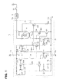
- FIG. 6 is a diagram showing an electrical configuration of a constant current supply device (IC) 211 having a plurality of current output terminals 212 corresponding to k channels and a plurality of constant current output circuits 213 each provided for one of the current output terminals 212 .
- FIG. 7 is a diagram showing a detailed electrical configuration of each of the constant current circuits 212 .
- the IC 211 comprises k current output terminals 212 and k constant current output circuits 213 each used for outputting a constant current of typically 1.3 A to an external load RL connected to one of the current output terminals 212 .
- the remaining circuit shown in FIG. 6 is an output current adjustment circuit 214 .
- a power supply line 215 for supplying a battery voltage VMAIN in the range 5.6 to 35 V is wired to the emitter of a PNP-type transistor Q 211 (first transistor) by a resistor R 211 (current detection resistor) and a resistor R 212 , which are connected to each other in series.
- the power supply line 215 is also wired to the emitter of a PNP-type transistor Q 212 (second transistor) by a resistor R 213 .
- the base of the transistor Q 211 is connected to the base of the transistor Q 212 and the base of the transistor Q 211 is connected to the collector of the transistor Q 211 so that, as a whole, a circuit configuration identical with that of a current mirror circuit is formed.
- the resistors R 211 , R 212 and R 213 are each an Al (aluminum) shunt resistor.
- a junction point between the resistors R 211 and R 212 is connected to the current output terminal 212 by a N-channel LDMOS transistor Q 213 (third transistor) functioning as an output transistor.
- the source of the transistor Q 213 is connected to the current output terminal 212 while the drain of the transistor Q 213 is connected to the junction point.
- the resistor R 211 for current detection use and the transistor Q 213 are connected to each other in series between the power supply line 215 and the current output terminal 212 .
- a PNP-type transistor Q 214 (fifth transistor) flows a portion of a feedback-control current flowing into the transistor Q 212 to a node Na shown in the figure.
- the transistor Q 214 is thus a component of the output current adjustment circuit 214 .
- the base of the transistor Q 214 is connected to the base of the transistor Q 212 and the emitter of the transistor Q 214 is connected to the emitter of the transistor Q 212 .
- the transistors Q 214 and Q 212 have a predetermined emitter area ratio.
- a ground line 216 is connected to the emitters of NPN-type transistors Q 215 and Q 216 , which form a current mirror circuit 218 .
- a voltage Vcc2 obtained as a result of a boosting operation carried out by a charge pump circuit to a level in the range 15V to 30V is supplied to a power supply line 217 connected to the emitters of PNP-type transistors Q 217 and Q 218 , which form a current mirror circuit 219 .
- the current mirror circuits 218 and 219 form a feedback control circuit 220 .
- the collector of the transistor Q 216 serves as an output-side node of the current mirror circuit 218 while the collector of the transistor Q 218 serves as an output-side node of the current mirror circuit 219 . These collectors are both connected to the gate of the transistor Q 213 .
- the collector or the base of the transistor Q 215 is a node on the input side of the current mirror circuit 218 .
- the collector and base of the transistor Q 215 are connected to the collector of the transistor Q 212 .
- the collector or the base of the transistor Q 217 is a node on the input side of the current mirror circuit 219 .
- a NPN-type transistor Q 219 is connected between the ground line 216 and the collector as well as base of the transistor Q 217 .
- a NPN-type transistor Q 219 is connected between the ground line 216 and the collector as well as base of the transistor Q 211 .
- the transistors Q 219 and Q 220 form a current mirror circuit in conjunction with the transistor Q 221 .
- a voltage Vcc of 5V is supplied to a power supply line 221 connected to the emitters of transistors Q 222 and Q 223 , which form a current mirror circuit.
- a constant current circuit 222 is connected between the ground line 216 and the collector (or the base) of the transistor Q 222 .
- the collector of a transistor Q 223 is connected to the collector (and base) of the transistor Q 221 .
- collector currents equal to a current I 1 output by the constant current circuit 222 flow through the transistors Q 217 to Q 220 .
- the circuit comprising the constant current circuit 222 and the transistors Q 221 to Q 223 can also be provided as a circuit common to all the constant current output circuits 213 .
- the collector of a NPN-type transistor Q 224 (fourth transistor) is connected to the node Na to which the shunt current Ia is output.
- the emitter of the transistor Q 224 is connected to the ground line 216 (second power supply line) by a resistor R 214 .
- the bases of the transistors Q 224 each provided for one of the constant current output circuits 213 are connected to the base of a transistor Q 225 (sixth transistor) to form a current mirror circuit.
- a constant current circuit 223 is connected between the collector of the transistor Q 225 and a power supply line 221 .
- the emitter of the transistor Q 225 is connected to the ground line 216 by a trimmable resistor R 215 .
- the constant current circuit 223 As well as the resistors R 214 and R 215 , form a reference current generation circuit 224 for flowing a reference current corresponding to the shunt current Ia.
- the reference current generation circuit 224 and the transistors Q 214 , Q 224 and Q 225 form the output current adjustment circuit 214 .
- the constant current circuit 223 generates a constant current on the basis of a voltage generated by a resistor potentiometer for dividing a voltage output by a band gap reference voltage circuit.
- the constant bias current I 1 flows through the transistors Q 218 and Q 220 . Accordingly, the current I 1 also flows through the transistor Q 211 .
- the power supply line 215 is connected to a battery, allowing the current Io to flow from the battery to the load RL by way of the power supply line 215 , the resistor R 211 , the transistor Q 213 and the output current terminal 212 of the IC 211 .
- the output current Io exceeds a predetermined target current magnitude.
- the voltage appearing between the two ends of the resistor R 211 rises, causing the voltage appearing between the base and emitter of the transistor Q 212 and, hence, the current flowing through the collector of the transistor Q 212 to increase.
- the current flowing through the collector of the transistor Q 212 flows to the current mirror circuit 218 , which comprises the transistors Q 215 and Q 216 . Since the constant current I 1 flows to the current mirror circuit 219 comprising the transistors Q 217 and Q 218 , on the other hand, the increase of the current flowing through the collector of the transistor Q 212 reduces the voltage appearing between the gate and source of the transistor Q 213 as a result of the negative feedback control. This negative feedback control restores the current flowing through the drain of the transistor Q 213 , that is, the output current Io, to the target magnitude.
- VBE(Q 211 ) denote the voltage appearing between the base and emitter of the transistor Q 211
- VBE(Q 212 ) denote the voltage appearing between the base and emitter of the transistor Q 212
- R 211 , R 212 and R 213 used in Eq. (6) represent the resistances of respective resistors R 211 , R 212 and R 213 , which are each an Al wire resistor so that a trimming process cannot be carried out on those resistors.
- a trimming process can be applied to the emitter area ratio m and the ratio Ic(Q 212 )/Ic(Q 211 ).
- the work to carry out a trimming process on the emitter area ratio m for all channels is very cumbersome.
- a portion of the current Ic(Q 212 ) flowing through the collector of the transistor Q 212 is diverted to flow into the transistor Q 214 as the current Ia subtracted from the current Ic(Q 212 ) so that the ratio Ic(Q 212 )/Ic(Q 211 ) can be adjusted to a variable value to trim the shunt current Ia collectively for all channels.
- the magnitude of the shunt current Ia is determined by the output current adjustment circuit 214 .
- the transistor Q 224 through which the shunt current Ia flows from the constant current output circuits 213 of all channels forms a current mirror circuit in conjunction with the transistor Q 225 .
- the shunt current Ia flowing through the transistor Q 224 common to all channels can be changed in an aggregated manner for all the channels.
- FIGS. 8 to 10 are each a diagram showing a result of simulation.
- the results of simulation were computed under conditions including a voltage Vcc of 5 V, a boosted voltage Vcc2 of 28 V, a battery voltage VMAIN of 18 V, a target output current of 1.3 A as well as junction temperatures of ⁇ 40 degrees Celsius corresponding to the dashed line shown in the figure, 25 degrees Celsius corresponding to the dot-and-dash line shown in the figure and 150 degrees Celsius corresponding to the solid line shown in the figure.
- FIG. 8 shows pre-trimming magnitudes of the output current Io with the resistances of all resistors in the constant current output circuit 213 increased from their predetermined values by +10% on the assumption of the existence of process dispersions.
- FIG. 9 shows post-trimming magnitudes of the output current Io, which were attained under the same condition as FIG. 8 except that the resistor R 215 of the output current adjustment circuit 214 was trimmed.
- FIG. 10 shows post-trimming magnitudes of the output current Io, which were attained under the same pre-trimming condition except that the emitter area ratio m was trimmed for all channels.
- the output current Io decreases from the target magnitude of 1.3 A to 1.2 A as shown in FIG. 8 .
- the output currents Io for all channels can be adjusted to about 1.3 A without regard to whether the junction temperatures are high or low as is obvious from FIG. 9 .
- the simulation result shown in FIG. 9 indicates that trimming of the resistor R 215 provided at only one location is a trimming process having precision at least the same as that of the process carried out on the conventional circuit to trim the emitter area ratios m for all channels as shown in FIG. 10 .
- this embodiment implementing the IC 211 including the constant current output circuits 213 for a plurality of channels is characterized in that the IC 211 has a configuration employing the additional output current adjustment circuit 214 .
- the output current adjustment circuit 214 has the transistor Q 224 for shunting a portion of a current flowing through the transistor Q 212 employed in each of the constant current output circuits 213 .
- the shunt current Ia and, hence, the output current Io are changed as a single quantity.
- the aggregated current adjustment for the constant current output circuits 213 can be carried out with ease and the time it takes to carry out the aggregated current adjustment can be shortened.
- the transistor Q 214 is added with the base and emitter of the transistor Q 214 connected to respectively the base and emitter of the transistor Q 212 . Since the shunt current Ia is flown to the transistor Q 224 by way of the transistor Q 214 , mutual interference of the constant current output circuit 213 and the output current adjustment circuit 214 can be suppressed.
- the output node of the current mirror circuit 218 inputting a current flowing through the collector of the transistor Q 212 and the output node of the current mirror circuit 219 inputting a constant current are connected to the gate of the transistor Q 213 to form the feedback control circuit 220 having a high gain.
- the output current Io can be adjusted in follow-up control to a target magnitude with a high degree of precision without regard to changes in power supply voltage and changes in load.
- an IC 225 comprises a plurality of constant current output circuits 213 .
- the IC 225 comprises k current output terminals 212 , k constant current output circuits 213 each used for outputting a constant current of typically 1.3 A to an external load RL connected to one of the current output terminals 212 and an output current adjustment circuit 226 .
- the output current adjustment circuit 226 comprises transistors Q 214 , Q 224 and Q 225 as well as a reference current generation circuit 227 .
- the transistors Q 224 and Q 225 form a current mirror circuit.
- the emitter of the transistor Q 225 is connected to the ground line 216 by a fixed resistor R 216 .
- the emitter area ratio of the transistor Q 224 is equal to that of the transistor Q 225 and the resistance of the resistor R 214 is exactly equal to that of a resistor R 216 .
- the reference current generation circuit 227 is a constant current circuit that can be subjected to a current adjusting process.
- the reference current generation circuit 227 comprises a current mirror circuit, a resistor R 217 , a trimmable resistor R 218 and a constant current circuit 228 .
- the current mirror circuit comprises PNP-type transistors Q 226 and Q 227 .
- the resistor R 217 is connected between the emitter of the transistor Q 226 and a power supply line 221 .
- the resistor R 218 is connected between the emitter of the transistor Q 227 and the power supply line 221 .
- the constant current circuit 228 is connected between the collector of the transistor Q 226 and the ground line 216 .
- the collector of the transistor Q 227 connected to the collector of the transistor Q 225 serves as an output node of the reference current generation circuit 227 .
- the transistor Q 214 can be eliminated to connect the collector of the transistor Q 215 directly to the collector of the transistor Q 224 .
- the resistors R 212 and R 213 can also be eliminated.
- the third embodiment can have a configuration in which a fixed resistor can be employed as the resistor R 215 and the transistor Q 225 can have a trimmable emitter area.
- the emitter area ratios of the transistors Q 224 can also be made different from each other, and the emitter area ratio of each of the transistors Q 224 can also be made different from that of the transistor Q 225 .
- the resistances of the resistors R 214 can also be made different from each other, and the resistance of each of the resistors R 214 can also be made different from the resistance of the resistor R 216 . In these cases, when the resistor R 218 is trimmed, the shunt currents Ia of the channels are all changed in accordance with a ratio determined by the emitter area ratios or the resistances.
- the resistors R 214 and R 216 can be eliminated.
- a Zener-zap-trimming technique or a fusion cutting trimming technique can be adopted.
- the transistors can each be a bipolar transistor or an FET, whereas the ICs 21 and 25 can each have a configuration comprising bipolar, CMOS and BiCMOS circuits.
Landscapes
- Engineering & Computer Science (AREA)
- Physics & Mathematics (AREA)
- Microelectronics & Electronic Packaging (AREA)
- Nonlinear Science (AREA)
- Electromagnetism (AREA)
- General Physics & Mathematics (AREA)
- Radar, Positioning & Navigation (AREA)
- Automation & Control Theory (AREA)
- Control Of Electrical Variables (AREA)
Abstract
Description
V(R 211)=(Ic(Q 211)+Io)×R 211 (1)
V(R 212)=Ic(Q 211)×R 212 (2)
V(R 213)=Ic(Q 212)×R 213 (3)
V(R 211)+V(R 212)+VBE(Q 211)=V(R 213)+VBE(Q 212) (4)
(Ic(Q 211)+Io)×R 211+Ic(Q 211)×R 212+VBE(Q 211)=Ic(Q 212)×R 213+V(R 213) (5)
Io=VT/
Claims (18)
Applications Claiming Priority (4)
| Application Number | Priority Date | Filing Date | Title |
|---|---|---|---|
| JP2003073898A JP4033009B2 (en) | 2003-03-18 | 2003-03-18 | Constant current control circuit |
| JP2003-73898 | 2003-03-18 | ||
| JP2003-395571 | 2003-11-26 | ||
| JP2003395571A JP4228890B2 (en) | 2003-11-26 | 2003-11-26 | Semiconductor integrated circuit device |
Publications (2)
| Publication Number | Publication Date |
|---|---|
| US20040183515A1 US20040183515A1 (en) | 2004-09-23 |
| US6954058B2 true US6954058B2 (en) | 2005-10-11 |
Family
ID=32992988
Family Applications (1)
| Application Number | Title | Priority Date | Filing Date |
|---|---|---|---|
| US10/795,323 Expired - Lifetime US6954058B2 (en) | 2003-03-18 | 2004-03-09 | Constant current supply device |
Country Status (1)
| Country | Link |
|---|---|
| US (1) | US6954058B2 (en) |
Cited By (8)
| Publication number | Priority date | Publication date | Assignee | Title |
|---|---|---|---|---|
| US20050001671A1 (en) * | 2003-06-19 | 2005-01-06 | Rohm Co., Ltd. | Constant voltage generator and electronic equipment using the same |
| US20060181257A1 (en) * | 2003-03-10 | 2006-08-17 | Koninklijke Philips Electronics., N.V. | Current mirror |
| US20070210836A1 (en) * | 2006-03-06 | 2007-09-13 | Francois Laulanet | Precision differential level shifter |
| US20080265947A1 (en) * | 2005-08-05 | 2008-10-30 | Denso Corporation | Current mirror circuit and constant current having the same |
| US20080284493A1 (en) * | 2007-05-18 | 2008-11-20 | Samsung Electronics Co., Ltd. | Proportional to absolute temperature current generation circuit having higher temperature coefficient, display device including the same, and method thereof |
| US20090085501A1 (en) * | 2007-09-27 | 2009-04-02 | Osram Sylvania, Inc. | Constant current driver circuit with voltage compensated current sense mirror |
| WO2012015591A1 (en) * | 2010-07-29 | 2012-02-02 | Iwatt Inc. | Dual output power supply |
| US20130083573A1 (en) * | 2011-10-04 | 2013-04-04 | SK Hynix Inc. | Regulator and high voltage generator |
Families Citing this family (9)
| Publication number | Priority date | Publication date | Assignee | Title |
|---|---|---|---|---|
| US7890232B2 (en) * | 2005-08-23 | 2011-02-15 | Fujitsu Ten Limited | Airbag system |
| US7804287B2 (en) * | 2007-02-28 | 2010-09-28 | Rockwell Automation Technologies, Inc. | Low heat dissipation I/O module using direct drive buck converter |
| JP5554134B2 (en) * | 2010-04-27 | 2014-07-23 | ローム株式会社 | Current generating circuit and reference voltage circuit using the same |
| CN102023669B (en) * | 2010-09-21 | 2013-10-16 | 上海大学 | A high-efficiency controllable constant current source circuit |
| JP5714924B2 (en) * | 2011-01-28 | 2015-05-07 | ラピスセミコンダクタ株式会社 | Voltage identification device and clock control device |
| JP5782346B2 (en) * | 2011-09-27 | 2015-09-24 | セイコーインスツル株式会社 | Reference voltage circuit |
| CN106786406B (en) * | 2015-12-14 | 2019-04-23 | 成都芯源系统有限公司 | Monolithically integrated switching device with secure operating area protection |
| DE102017205618B4 (en) * | 2017-04-03 | 2026-02-12 | Robert Bosch Gmbh | Device and method for providing an activation voltage for a safety device for a vehicle and safety device |
| GB2639774A (en) * | 2023-04-28 | 2025-10-01 | Boe Technology Group Co Ltd | Scan circuit, array substrate, and display apparatus |
Citations (6)
| Publication number | Priority date | Publication date | Assignee | Title |
|---|---|---|---|---|
| US4088941A (en) * | 1976-10-05 | 1978-05-09 | Rca Corporation | Voltage reference circuits |
| JPH0535352A (en) | 1991-07-30 | 1993-02-12 | Sharp Corp | Constant current circuit |
| JP2000124743A (en) | 1998-10-19 | 2000-04-28 | Texas Instr Japan Ltd | Current source circuit |
| US6087821A (en) | 1998-10-07 | 2000-07-11 | Ricoh Company, Ltd. | Reference-voltage generating circuit |
| JP2002091589A (en) | 2000-09-18 | 2002-03-29 | Fuji Electric Co Ltd | Reference voltage circuit and trimming method thereof |
| JP2002236521A (en) | 2001-02-07 | 2002-08-23 | Ricoh Co Ltd | Constant current circuit, triangular wave generation circuit and lamp voltage generation circuit using the constant current circuit |
-
2004
- 2004-03-09 US US10/795,323 patent/US6954058B2/en not_active Expired - Lifetime
Patent Citations (6)
| Publication number | Priority date | Publication date | Assignee | Title |
|---|---|---|---|---|
| US4088941A (en) * | 1976-10-05 | 1978-05-09 | Rca Corporation | Voltage reference circuits |
| JPH0535352A (en) | 1991-07-30 | 1993-02-12 | Sharp Corp | Constant current circuit |
| US6087821A (en) | 1998-10-07 | 2000-07-11 | Ricoh Company, Ltd. | Reference-voltage generating circuit |
| JP2000124743A (en) | 1998-10-19 | 2000-04-28 | Texas Instr Japan Ltd | Current source circuit |
| JP2002091589A (en) | 2000-09-18 | 2002-03-29 | Fuji Electric Co Ltd | Reference voltage circuit and trimming method thereof |
| JP2002236521A (en) | 2001-02-07 | 2002-08-23 | Ricoh Co Ltd | Constant current circuit, triangular wave generation circuit and lamp voltage generation circuit using the constant current circuit |
Cited By (21)
| Publication number | Priority date | Publication date | Assignee | Title |
|---|---|---|---|---|
| US7352235B2 (en) * | 2003-03-10 | 2008-04-01 | Nxp B.V. | Current mirror |
| US20060181257A1 (en) * | 2003-03-10 | 2006-08-17 | Koninklijke Philips Electronics., N.V. | Current mirror |
| US7023181B2 (en) * | 2003-06-19 | 2006-04-04 | Rohm Co., Ltd. | Constant voltage generator and electronic equipment using the same |
| US20060125461A1 (en) * | 2003-06-19 | 2006-06-15 | Rohm Co., Ltd. | Constant voltage generator and electronic equipment using the same |
| US7151365B2 (en) | 2003-06-19 | 2006-12-19 | Rohm Co., Ltd. | Constant voltage generator and electronic equipment using the same |
| US20050001671A1 (en) * | 2003-06-19 | 2005-01-06 | Rohm Co., Ltd. | Constant voltage generator and electronic equipment using the same |
| US20080265947A1 (en) * | 2005-08-05 | 2008-10-30 | Denso Corporation | Current mirror circuit and constant current having the same |
| US7498868B2 (en) | 2005-08-05 | 2009-03-03 | Denso Corporation | Current mirror circuit and constant current circuit having the same |
| US7551003B2 (en) * | 2005-08-05 | 2009-06-23 | Denso Corporation | Current mirror circuit and constant current circuit having the same |
| US20070210836A1 (en) * | 2006-03-06 | 2007-09-13 | Francois Laulanet | Precision differential level shifter |
| US7696786B2 (en) * | 2006-03-06 | 2010-04-13 | On Semiconductor | Precision differential level shifter |
| US8994444B2 (en) * | 2007-05-18 | 2015-03-31 | Samsung Electronics Co., Ltd. | Proportional to absolute temperature current generation circuit having higher temperature coefficient, display device including the same, and method thereof |
| US20080284493A1 (en) * | 2007-05-18 | 2008-11-20 | Samsung Electronics Co., Ltd. | Proportional to absolute temperature current generation circuit having higher temperature coefficient, display device including the same, and method thereof |
| US20090085501A1 (en) * | 2007-09-27 | 2009-04-02 | Osram Sylvania, Inc. | Constant current driver circuit with voltage compensated current sense mirror |
| US20100308750A1 (en) * | 2007-09-27 | 2010-12-09 | Osram Sylvania Inc. | Constant current driver circuit with voltage compensated current sense mirror |
| US7973488B2 (en) * | 2007-09-27 | 2011-07-05 | Osram Sylvania Inc. | Constant current driver circuit with voltage compensated current sense mirror |
| US7781985B2 (en) * | 2007-09-27 | 2010-08-24 | Osram Sylvania Inc. | Constant current driver circuit with voltage compensated current sense mirror |
| WO2012015591A1 (en) * | 2010-07-29 | 2012-02-02 | Iwatt Inc. | Dual output power supply |
| US8933582B2 (en) | 2010-07-29 | 2015-01-13 | Dialog Semiconductor Inc. | Dual output power supply |
| US20130083573A1 (en) * | 2011-10-04 | 2013-04-04 | SK Hynix Inc. | Regulator and high voltage generator |
| US8872489B2 (en) * | 2011-10-04 | 2014-10-28 | SK Hynix Inc. | Regulator and high voltage generator including the same |
Also Published As
| Publication number | Publication date |
|---|---|
| US20040183515A1 (en) | 2004-09-23 |
Similar Documents
| Publication | Publication Date | Title |
|---|---|---|
| US6954058B2 (en) | Constant current supply device | |
| US5861771A (en) | Regulator circuit and semiconductor integrated circuit device having the same | |
| US5570008A (en) | Band gap reference voltage source | |
| JPH08234853A (en) | Ptat electric current source | |
| US7902913B2 (en) | Reference voltage generation circuit | |
| JP2010218543A (en) | Voltage regulator | |
| JP2002108465A (en) | Temperature detection circuit and overheat protection circuit, and various electronic devices incorporating these circuits | |
| US6060871A (en) | Stable voltage regulator having first-order and second-order output voltage compensation | |
| US8054156B2 (en) | Low variation resistor | |
| US4831323A (en) | Voltage limiting circuit | |
| KR100630398B1 (en) | Voltage regulator circuit having short-circuit protection circuit | |
| EP1220071B1 (en) | Semiconductor device | |
| US11762410B2 (en) | Voltage reference with temperature-selective second-order temperature compensation | |
| US7638996B2 (en) | Reference current generator circuit | |
| US7518437B2 (en) | Constant current circuit and constant current generating method | |
| US8624610B2 (en) | Synthesized current sense resistor for wide current sense range | |
| US12554279B2 (en) | Voltage regulator circuit and method for providing a regulated voltage | |
| JP3334707B2 (en) | Charge pump circuit | |
| US7535279B2 (en) | Versatile control pin electronics | |
| JP2000175441A (en) | Charge pump circuit | |
| US20090058390A1 (en) | Semiconductor device with compensation current | |
| US7358713B2 (en) | Constant voltage source with output current limitation | |
| JP4228890B2 (en) | Semiconductor integrated circuit device | |
| JP2006260209A (en) | Voltage controlling voltage source | |
| US20250258511A1 (en) | Semiconductor device |
Legal Events
| Date | Code | Title | Description |
|---|---|---|---|
| AS | Assignment |
Owner name: DENSO CORPORATION, JAPAN Free format text: ASSIGNMENT OF ASSIGNORS INTEREST;ASSIGNORS:OTA, KINGO;OKUDA, SHOICHI;REEL/FRAME:015092/0190;SIGNING DATES FROM 20040218 TO 20040219 |
|
| STCF | Information on status: patent grant |
Free format text: PATENTED CASE |
|
| FEPP | Fee payment procedure |
Free format text: PAYOR NUMBER ASSIGNED (ORIGINAL EVENT CODE: ASPN); ENTITY STATUS OF PATENT OWNER: LARGE ENTITY |
|
| FPAY | Fee payment |
Year of fee payment: 4 |
|
| FEPP | Fee payment procedure |
Free format text: PAYOR NUMBER ASSIGNED (ORIGINAL EVENT CODE: ASPN); ENTITY STATUS OF PATENT OWNER: LARGE ENTITY Free format text: PAYER NUMBER DE-ASSIGNED (ORIGINAL EVENT CODE: RMPN); ENTITY STATUS OF PATENT OWNER: LARGE ENTITY |
|
| FPAY | Fee payment |
Year of fee payment: 8 |
|
| FPAY | Fee payment |
Year of fee payment: 12 |