EP0789400A2 - Dispositif semi-conducteur et méthode de fabrication - Google Patents
Dispositif semi-conducteur et méthode de fabrication Download PDFInfo
- Publication number
- EP0789400A2 EP0789400A2 EP97101990A EP97101990A EP0789400A2 EP 0789400 A2 EP0789400 A2 EP 0789400A2 EP 97101990 A EP97101990 A EP 97101990A EP 97101990 A EP97101990 A EP 97101990A EP 0789400 A2 EP0789400 A2 EP 0789400A2
- Authority
- EP
- European Patent Office
- Prior art keywords
- region
- semiconductor device
- impurity
- nitrogen
- gate electrode
- Prior art date
- Legal status (The legal status is an assumption and is not a legal conclusion. Google has not performed a legal analysis and makes no representation as to the accuracy of the status listed.)
- Withdrawn
Links
- 238000000034 method Methods 0.000 title claims abstract description 154
- 239000004065 semiconductor Substances 0.000 title claims abstract description 138
- IJGRMHOSHXDMSA-UHFFFAOYSA-N Atomic nitrogen Chemical compound N#N IJGRMHOSHXDMSA-UHFFFAOYSA-N 0.000 claims abstract description 333
- 229910052757 nitrogen Inorganic materials 0.000 claims abstract description 176
- 239000012535 impurity Substances 0.000 claims abstract description 164
- 239000000758 substrate Substances 0.000 claims abstract description 157
- 238000009792 diffusion process Methods 0.000 claims abstract description 133
- 239000007943 implant Substances 0.000 claims abstract description 129
- 150000002500 ions Chemical class 0.000 claims abstract description 90
- 230000005669 field effect Effects 0.000 claims abstract description 83
- 230000015572 biosynthetic process Effects 0.000 claims abstract description 70
- 238000011282 treatment Methods 0.000 claims description 55
- 238000005389 semiconductor device fabrication Methods 0.000 claims description 49
- 238000004519 manufacturing process Methods 0.000 claims description 42
- QGZKDVFQNNGYKY-UHFFFAOYSA-N Ammonia Chemical compound N QGZKDVFQNNGYKY-UHFFFAOYSA-N 0.000 claims description 39
- 238000000137 annealing Methods 0.000 claims description 39
- 229910021332 silicide Inorganic materials 0.000 claims description 28
- FVBUAEGBCNSCDD-UHFFFAOYSA-N silicide(4-) Chemical compound [Si-4] FVBUAEGBCNSCDD-UHFFFAOYSA-N 0.000 claims description 28
- -1 nitrogen ions Chemical class 0.000 claims description 26
- 238000009413 insulation Methods 0.000 claims description 25
- 239000007789 gas Substances 0.000 claims description 18
- 238000009826 distribution Methods 0.000 claims description 16
- 239000004020 conductor Substances 0.000 claims description 14
- 230000007423 decrease Effects 0.000 claims description 9
- 230000007547 defect Effects 0.000 claims description 9
- 238000000151 deposition Methods 0.000 claims description 9
- 210000002381 plasma Anatomy 0.000 claims description 9
- 230000003247 decreasing effect Effects 0.000 claims description 5
- 238000001514 detection method Methods 0.000 claims description 5
- 230000007812 deficiency Effects 0.000 claims description 3
- 229910052751 metal Inorganic materials 0.000 claims description 3
- 239000002184 metal Substances 0.000 claims description 3
- 239000011810 insulating material Substances 0.000 claims description 2
- 238000000059 patterning Methods 0.000 claims description 2
- 239000012212 insulator Substances 0.000 claims 2
- XUIMIQQOPSSXEZ-UHFFFAOYSA-N Silicon Chemical compound [Si] XUIMIQQOPSSXEZ-UHFFFAOYSA-N 0.000 abstract description 60
- 229910052710 silicon Inorganic materials 0.000 abstract description 60
- 239000010703 silicon Substances 0.000 abstract description 60
- 239000010408 film Substances 0.000 description 159
- 239000010410 layer Substances 0.000 description 155
- 229910052796 boron Inorganic materials 0.000 description 71
- ZOXJGFHDIHLPTG-UHFFFAOYSA-N Boron Chemical compound [B] ZOXJGFHDIHLPTG-UHFFFAOYSA-N 0.000 description 69
- 229910015900 BF3 Inorganic materials 0.000 description 50
- WTEOIRVLGSZEPR-UHFFFAOYSA-N boron trifluoride Chemical compound FB(F)F WTEOIRVLGSZEPR-UHFFFAOYSA-N 0.000 description 46
- 230000000694 effects Effects 0.000 description 38
- 238000004151 rapid thermal annealing Methods 0.000 description 31
- 230000015556 catabolic process Effects 0.000 description 26
- 238000006731 degradation reaction Methods 0.000 description 24
- 229910052785 arsenic Inorganic materials 0.000 description 22
- RQNWIZPPADIBDY-UHFFFAOYSA-N arsenic atom Chemical compound [As] RQNWIZPPADIBDY-UHFFFAOYSA-N 0.000 description 21
- 229910021420 polycrystalline silicon Inorganic materials 0.000 description 16
- 229920005591 polysilicon Polymers 0.000 description 16
- 229920002120 photoresistant polymer Polymers 0.000 description 14
- 238000012545 processing Methods 0.000 description 13
- 238000001994 activation Methods 0.000 description 12
- 238000002513 implantation Methods 0.000 description 12
- 230000004913 activation Effects 0.000 description 11
- 230000008901 benefit Effects 0.000 description 11
- 230000009467 reduction Effects 0.000 description 9
- 230000035515 penetration Effects 0.000 description 8
- VYPSYNLAJGMNEJ-UHFFFAOYSA-N Silicium dioxide Chemical compound O=[Si]=O VYPSYNLAJGMNEJ-UHFFFAOYSA-N 0.000 description 7
- 229910052814 silicon oxide Inorganic materials 0.000 description 7
- 239000012141 concentrate Substances 0.000 description 6
- 230000008021 deposition Effects 0.000 description 6
- 238000010586 diagram Methods 0.000 description 6
- 238000001312 dry etching Methods 0.000 description 6
- 230000008569 process Effects 0.000 description 6
- 239000010936 titanium Substances 0.000 description 6
- 239000000969 carrier Substances 0.000 description 5
- 239000000203 mixture Substances 0.000 description 5
- 230000003071 parasitic effect Effects 0.000 description 5
- 238000000206 photolithography Methods 0.000 description 5
- XKRFYHLGVUSROY-UHFFFAOYSA-N Argon Chemical compound [Ar] XKRFYHLGVUSROY-UHFFFAOYSA-N 0.000 description 4
- 238000005121 nitriding Methods 0.000 description 4
- 230000003647 oxidation Effects 0.000 description 4
- 238000007254 oxidation reaction Methods 0.000 description 4
- PXGOKWXKJXAPGV-UHFFFAOYSA-N Fluorine Chemical compound FF PXGOKWXKJXAPGV-UHFFFAOYSA-N 0.000 description 3
- OAICVXFJPJFONN-UHFFFAOYSA-N Phosphorus Chemical compound [P] OAICVXFJPJFONN-UHFFFAOYSA-N 0.000 description 3
- 230000003321 amplification Effects 0.000 description 3
- 238000013459 approach Methods 0.000 description 3
- 230000009977 dual effect Effects 0.000 description 3
- 229910052731 fluorine Inorganic materials 0.000 description 3
- 239000011737 fluorine Substances 0.000 description 3
- 238000003199 nucleic acid amplification method Methods 0.000 description 3
- 229910052698 phosphorus Inorganic materials 0.000 description 3
- 239000011574 phosphorus Substances 0.000 description 3
- 229910052787 antimony Inorganic materials 0.000 description 2
- WATWJIUSRGPENY-UHFFFAOYSA-N antimony atom Chemical compound [Sb] WATWJIUSRGPENY-UHFFFAOYSA-N 0.000 description 2
- 229910052786 argon Inorganic materials 0.000 description 2
- 238000010420 art technique Methods 0.000 description 2
- 230000005465 channeling Effects 0.000 description 2
- 238000005229 chemical vapour deposition Methods 0.000 description 2
- 238000007796 conventional method Methods 0.000 description 2
- 230000000779 depleting effect Effects 0.000 description 2
- 229910001873 dinitrogen Inorganic materials 0.000 description 2
- 238000005516 engineering process Methods 0.000 description 2
- 229910052738 indium Inorganic materials 0.000 description 2
- APFVFJFRJDLVQX-UHFFFAOYSA-N indium atom Chemical compound [In] APFVFJFRJDLVQX-UHFFFAOYSA-N 0.000 description 2
- 238000005468 ion implantation Methods 0.000 description 2
- 238000005259 measurement Methods 0.000 description 2
- 150000004767 nitrides Chemical class 0.000 description 2
- 229910000069 nitrogen hydride Inorganic materials 0.000 description 2
- 238000001020 plasma etching Methods 0.000 description 2
- 125000006850 spacer group Chemical group 0.000 description 2
- 229910052721 tungsten Inorganic materials 0.000 description 2
- 239000010937 tungsten Substances 0.000 description 2
- UFHFLCQGNIYNRP-UHFFFAOYSA-N Hydrogen Chemical compound [H][H] UFHFLCQGNIYNRP-UHFFFAOYSA-N 0.000 description 1
- BOTDANWDWHJENH-UHFFFAOYSA-N Tetraethyl orthosilicate Chemical compound CCO[Si](OCC)(OCC)OCC BOTDANWDWHJENH-UHFFFAOYSA-N 0.000 description 1
- RTAQQCXQSZGOHL-UHFFFAOYSA-N Titanium Chemical compound [Ti] RTAQQCXQSZGOHL-UHFFFAOYSA-N 0.000 description 1
- 229910021529 ammonia Inorganic materials 0.000 description 1
- 229910052799 carbon Inorganic materials 0.000 description 1
- 238000001816 cooling Methods 0.000 description 1
- 238000010494 dissociation reaction Methods 0.000 description 1
- 230000005593 dissociations Effects 0.000 description 1
- 239000002784 hot electron Substances 0.000 description 1
- BHEPBYXIRTUNPN-UHFFFAOYSA-N hydridophosphorus(.) (triplet) Chemical compound [PH] BHEPBYXIRTUNPN-UHFFFAOYSA-N 0.000 description 1
- 239000001257 hydrogen Substances 0.000 description 1
- 229910052739 hydrogen Inorganic materials 0.000 description 1
- 239000011261 inert gas Substances 0.000 description 1
- 239000011229 interlayer Substances 0.000 description 1
- 239000010416 ion conductor Substances 0.000 description 1
- 238000002955 isolation Methods 0.000 description 1
- 238000001459 lithography Methods 0.000 description 1
- 238000004518 low pressure chemical vapour deposition Methods 0.000 description 1
- 238000002844 melting Methods 0.000 description 1
- 230000008018 melting Effects 0.000 description 1
- 238000012986 modification Methods 0.000 description 1
- 150000002829 nitrogen Chemical class 0.000 description 1
- 230000002265 prevention Effects 0.000 description 1
- 238000004544 sputter deposition Methods 0.000 description 1
- 230000003068 static effect Effects 0.000 description 1
- 239000010409 thin film Substances 0.000 description 1
- 229910052719 titanium Inorganic materials 0.000 description 1
- 229910021341 titanium silicide Inorganic materials 0.000 description 1
- WFKWXMTUELFFGS-UHFFFAOYSA-N tungsten Chemical compound [W] WFKWXMTUELFFGS-UHFFFAOYSA-N 0.000 description 1
- 238000001039 wet etching Methods 0.000 description 1
Images


Classifications
-
- H—ELECTRICITY
- H01—ELECTRIC ELEMENTS
- H01L—SEMICONDUCTOR DEVICES NOT COVERED BY CLASS H10
- H01L21/00—Processes or apparatus adapted for the manufacture or treatment of semiconductor or solid state devices or of parts thereof
- H01L21/02—Manufacture or treatment of semiconductor devices or of parts thereof
- H01L21/04—Manufacture or treatment of semiconductor devices or of parts thereof the devices having at least one potential-jump barrier or surface barrier, e.g. PN junction, depletion layer or carrier concentration layer
- H01L21/18—Manufacture or treatment of semiconductor devices or of parts thereof the devices having at least one potential-jump barrier or surface barrier, e.g. PN junction, depletion layer or carrier concentration layer the devices having semiconductor bodies comprising elements of Group IV of the Periodic System or AIIIBV compounds with or without impurities, e.g. doping materials
- H01L21/26—Bombardment with radiation
- H01L21/263—Bombardment with radiation with high-energy radiation
- H01L21/265—Bombardment with radiation with high-energy radiation producing ion implantation
- H01L21/26506—Bombardment with radiation with high-energy radiation producing ion implantation in group IV semiconductors
-
- H—ELECTRICITY
- H01—ELECTRIC ELEMENTS
- H01L—SEMICONDUCTOR DEVICES NOT COVERED BY CLASS H10
- H01L21/00—Processes or apparatus adapted for the manufacture or treatment of semiconductor or solid state devices or of parts thereof
- H01L21/02—Manufacture or treatment of semiconductor devices or of parts thereof
- H01L21/04—Manufacture or treatment of semiconductor devices or of parts thereof the devices having at least one potential-jump barrier or surface barrier, e.g. PN junction, depletion layer or carrier concentration layer
- H01L21/18—Manufacture or treatment of semiconductor devices or of parts thereof the devices having at least one potential-jump barrier or surface barrier, e.g. PN junction, depletion layer or carrier concentration layer the devices having semiconductor bodies comprising elements of Group IV of the Periodic System or AIIIBV compounds with or without impurities, e.g. doping materials
- H01L21/28—Manufacture of electrodes on semiconductor bodies using processes or apparatus not provided for in groups H01L21/20 - H01L21/268
- H01L21/28008—Making conductor-insulator-semiconductor electrodes
- H01L21/28017—Making conductor-insulator-semiconductor electrodes the insulator being formed after the semiconductor body, the semiconductor being silicon
- H01L21/28158—Making the insulator
- H01L21/28167—Making the insulator on single crystalline silicon, e.g. using a liquid, i.e. chemical oxidation
- H01L21/28176—Making the insulator on single crystalline silicon, e.g. using a liquid, i.e. chemical oxidation with a treatment, e.g. annealing, after the formation of the definitive gate conductor
-
- H—ELECTRICITY
- H01—ELECTRIC ELEMENTS
- H01L—SEMICONDUCTOR DEVICES NOT COVERED BY CLASS H10
- H01L29/00—Semiconductor devices adapted for rectifying, amplifying, oscillating or switching, or capacitors or resistors with at least one potential-jump barrier or surface barrier, e.g. PN junction depletion layer or carrier concentration layer; Details of semiconductor bodies or of electrodes thereof ; Multistep manufacturing processes therefor
- H01L29/40—Electrodes ; Multistep manufacturing processes therefor
- H01L29/43—Electrodes ; Multistep manufacturing processes therefor characterised by the materials of which they are formed
- H01L29/49—Metal-insulator-semiconductor electrodes, e.g. gates of MOSFET
- H01L29/51—Insulating materials associated therewith
- H01L29/511—Insulating materials associated therewith with a compositional variation, e.g. multilayer structures
- H01L29/512—Insulating materials associated therewith with a compositional variation, e.g. multilayer structures the variation being parallel to the channel plane
-
- H—ELECTRICITY
- H01—ELECTRIC ELEMENTS
- H01L—SEMICONDUCTOR DEVICES NOT COVERED BY CLASS H10
- H01L29/00—Semiconductor devices adapted for rectifying, amplifying, oscillating or switching, or capacitors or resistors with at least one potential-jump barrier or surface barrier, e.g. PN junction depletion layer or carrier concentration layer; Details of semiconductor bodies or of electrodes thereof ; Multistep manufacturing processes therefor
- H01L29/66—Types of semiconductor device ; Multistep manufacturing processes therefor
- H01L29/66007—Multistep manufacturing processes
- H01L29/66075—Multistep manufacturing processes of devices having semiconductor bodies comprising group 14 or group 13/15 materials
- H01L29/66227—Multistep manufacturing processes of devices having semiconductor bodies comprising group 14 or group 13/15 materials the devices being controllable only by the electric current supplied or the electric potential applied, to an electrode which does not carry the current to be rectified, amplified or switched, e.g. three-terminal devices
- H01L29/66234—Bipolar junction transistors [BJT]
- H01L29/66272—Silicon vertical transistors
-
- H—ELECTRICITY
- H01—ELECTRIC ELEMENTS
- H01L—SEMICONDUCTOR DEVICES NOT COVERED BY CLASS H10
- H01L29/00—Semiconductor devices adapted for rectifying, amplifying, oscillating or switching, or capacitors or resistors with at least one potential-jump barrier or surface barrier, e.g. PN junction depletion layer or carrier concentration layer; Details of semiconductor bodies or of electrodes thereof ; Multistep manufacturing processes therefor
- H01L29/66—Types of semiconductor device ; Multistep manufacturing processes therefor
- H01L29/66007—Multistep manufacturing processes
- H01L29/66075—Multistep manufacturing processes of devices having semiconductor bodies comprising group 14 or group 13/15 materials
- H01L29/66227—Multistep manufacturing processes of devices having semiconductor bodies comprising group 14 or group 13/15 materials the devices being controllable only by the electric current supplied or the electric potential applied, to an electrode which does not carry the current to be rectified, amplified or switched, e.g. three-terminal devices
- H01L29/66409—Unipolar field-effect transistors
- H01L29/66477—Unipolar field-effect transistors with an insulated gate, i.e. MISFET
- H01L29/66568—Lateral single gate silicon transistors
- H01L29/66575—Lateral single gate silicon transistors where the source and drain or source and drain extensions are self-aligned to the sides of the gate
- H01L29/6659—Lateral single gate silicon transistors where the source and drain or source and drain extensions are self-aligned to the sides of the gate with both lightly doped source and drain extensions and source and drain self-aligned to the sides of the gate, e.g. lightly doped drain [LDD] MOSFET, double diffused drain [DDD] MOSFET
-
- H—ELECTRICITY
- H01—ELECTRIC ELEMENTS
- H01L—SEMICONDUCTOR DEVICES NOT COVERED BY CLASS H10
- H01L29/00—Semiconductor devices adapted for rectifying, amplifying, oscillating or switching, or capacitors or resistors with at least one potential-jump barrier or surface barrier, e.g. PN junction depletion layer or carrier concentration layer; Details of semiconductor bodies or of electrodes thereof ; Multistep manufacturing processes therefor
- H01L29/66—Types of semiconductor device ; Multistep manufacturing processes therefor
- H01L29/68—Types of semiconductor device ; Multistep manufacturing processes therefor controllable by only the electric current supplied, or only the electric potential applied, to an electrode which does not carry the current to be rectified, amplified or switched
- H01L29/70—Bipolar devices
- H01L29/72—Transistor-type devices, i.e. able to continuously respond to applied control signals
- H01L29/73—Bipolar junction transistors
- H01L29/732—Vertical transistors
- H01L29/7322—Vertical transistors having emitter-base and base-collector junctions leaving at the same surface of the body, e.g. planar transistor
-
- H—ELECTRICITY
- H01—ELECTRIC ELEMENTS
- H01L—SEMICONDUCTOR DEVICES NOT COVERED BY CLASS H10
- H01L29/00—Semiconductor devices adapted for rectifying, amplifying, oscillating or switching, or capacitors or resistors with at least one potential-jump barrier or surface barrier, e.g. PN junction depletion layer or carrier concentration layer; Details of semiconductor bodies or of electrodes thereof ; Multistep manufacturing processes therefor
- H01L29/66—Types of semiconductor device ; Multistep manufacturing processes therefor
- H01L29/68—Types of semiconductor device ; Multistep manufacturing processes therefor controllable by only the electric current supplied, or only the electric potential applied, to an electrode which does not carry the current to be rectified, amplified or switched
- H01L29/76—Unipolar devices, e.g. field effect transistors
- H01L29/772—Field effect transistors
- H01L29/78—Field effect transistors with field effect produced by an insulated gate
- H01L29/7833—Field effect transistors with field effect produced by an insulated gate with lightly doped drain or source extension, e.g. LDD MOSFET's; DDD MOSFET's
-
- H—ELECTRICITY
- H01—ELECTRIC ELEMENTS
- H01L—SEMICONDUCTOR DEVICES NOT COVERED BY CLASS H10
- H01L21/00—Processes or apparatus adapted for the manufacture or treatment of semiconductor or solid state devices or of parts thereof
- H01L21/02—Manufacture or treatment of semiconductor devices or of parts thereof
- H01L21/04—Manufacture or treatment of semiconductor devices or of parts thereof the devices having at least one potential-jump barrier or surface barrier, e.g. PN junction, depletion layer or carrier concentration layer
- H01L21/18—Manufacture or treatment of semiconductor devices or of parts thereof the devices having at least one potential-jump barrier or surface barrier, e.g. PN junction, depletion layer or carrier concentration layer the devices having semiconductor bodies comprising elements of Group IV of the Periodic System or AIIIBV compounds with or without impurities, e.g. doping materials
- H01L21/26—Bombardment with radiation
- H01L21/263—Bombardment with radiation with high-energy radiation
- H01L21/265—Bombardment with radiation with high-energy radiation producing ion implantation
- H01L21/26506—Bombardment with radiation with high-energy radiation producing ion implantation in group IV semiconductors
- H01L21/26513—Bombardment with radiation with high-energy radiation producing ion implantation in group IV semiconductors of electrically active species
-
- H—ELECTRICITY
- H01—ELECTRIC ELEMENTS
- H01L—SEMICONDUCTOR DEVICES NOT COVERED BY CLASS H10
- H01L21/00—Processes or apparatus adapted for the manufacture or treatment of semiconductor or solid state devices or of parts thereof
- H01L21/02—Manufacture or treatment of semiconductor devices or of parts thereof
- H01L21/04—Manufacture or treatment of semiconductor devices or of parts thereof the devices having at least one potential-jump barrier or surface barrier, e.g. PN junction, depletion layer or carrier concentration layer
- H01L21/18—Manufacture or treatment of semiconductor devices or of parts thereof the devices having at least one potential-jump barrier or surface barrier, e.g. PN junction, depletion layer or carrier concentration layer the devices having semiconductor bodies comprising elements of Group IV of the Periodic System or AIIIBV compounds with or without impurities, e.g. doping materials
- H01L21/26—Bombardment with radiation
- H01L21/263—Bombardment with radiation with high-energy radiation
- H01L21/265—Bombardment with radiation with high-energy radiation producing ion implantation
- H01L21/2658—Bombardment with radiation with high-energy radiation producing ion implantation of a molecular ion, e.g. decaborane
-
- H—ELECTRICITY
- H01—ELECTRIC ELEMENTS
- H01L—SEMICONDUCTOR DEVICES NOT COVERED BY CLASS H10
- H01L21/00—Processes or apparatus adapted for the manufacture or treatment of semiconductor or solid state devices or of parts thereof
- H01L21/02—Manufacture or treatment of semiconductor devices or of parts thereof
- H01L21/04—Manufacture or treatment of semiconductor devices or of parts thereof the devices having at least one potential-jump barrier or surface barrier, e.g. PN junction, depletion layer or carrier concentration layer
- H01L21/18—Manufacture or treatment of semiconductor devices or of parts thereof the devices having at least one potential-jump barrier or surface barrier, e.g. PN junction, depletion layer or carrier concentration layer the devices having semiconductor bodies comprising elements of Group IV of the Periodic System or AIIIBV compounds with or without impurities, e.g. doping materials
- H01L21/26—Bombardment with radiation
- H01L21/263—Bombardment with radiation with high-energy radiation
- H01L21/265—Bombardment with radiation with high-energy radiation producing ion implantation
- H01L21/26586—Bombardment with radiation with high-energy radiation producing ion implantation characterised by the angle between the ion beam and the crystal planes or the main crystal surface
-
- H—ELECTRICITY
- H01—ELECTRIC ELEMENTS
- H01L—SEMICONDUCTOR DEVICES NOT COVERED BY CLASS H10
- H01L29/00—Semiconductor devices adapted for rectifying, amplifying, oscillating or switching, or capacitors or resistors with at least one potential-jump barrier or surface barrier, e.g. PN junction depletion layer or carrier concentration layer; Details of semiconductor bodies or of electrodes thereof ; Multistep manufacturing processes therefor
- H01L29/40—Electrodes ; Multistep manufacturing processes therefor
- H01L29/43—Electrodes ; Multistep manufacturing processes therefor characterised by the materials of which they are formed
- H01L29/49—Metal-insulator-semiconductor electrodes, e.g. gates of MOSFET
- H01L29/51—Insulating materials associated therewith
- H01L29/518—Insulating materials associated therewith the insulating material containing nitrogen, e.g. nitride, oxynitride, nitrogen-doped material
Definitions
- the present invention relates to semiconductor devices having thereon MIS-type field effect transistors and bipolar transistors, and to a method of fabricating such semiconductor devices.
- the present invention pertains particularly to ways of increasing the performance and reliability of semiconductor devices by providing improved structures for impurity diffusion layers and gate insulation films.
- the gate oxide film plays a very important role.
- semiconductor devices which are element-miniaturized, which can be driven at low power and which can operate at high speed.
- it is necessary to sophisticatedly contrive not only the physical dimensions of gate oxide films (e.g., the film thickness) but also the structure thereof.
- CMOS devices in particular, hot carriers of nMOS transistors
- an oxynitride layer is formed in a gate oxide film.
- a technique has been reported in a paper (IEDM Tech. Dig. pp. 325-328, IEEE 1993), in which after formation of a gate electrode nitrogen ions are implanted into the gate electrode and into the semiconductor substrate, and the implanted nitrogen is diffused by an annealing treatment to form an oxynitride layer in the gate oxide film. This method is used as an example for describing the steps of forming an oxynitride layer.
- element isolator 4 is formed in a portion of silicon substrate 1 . Thereafter, an oxide film is formed on silicon substrate 1 within an active region surrounded by element isolator 4 , and a polysilicon film is deposited. Both the oxide film and the polysilicon film are patterned using photolithography and dry etching, to form gate oxide film 2 and gate electrode 3 .
- an ion implant is carried out in which ions of nitrogen (N+) are implanted, from above the substrate, into gate electrode 3 and into silicon substrate 1 within the active region.
- the implanted nitrogen ions are then diffused by an annealing treatment, to simultaneously form oxynitride layer 5 in gate oxide film 2 , and nitrogen diffusion layer 6 in a near-surface area of silicon substrate 1 .
- ions of arsenic (As+) of low concentration are implanted at approximately right angles to the surface of silicon substrate 1 , to form lightly-doped n-type source/drain region 7 at a near-surface area of silicon substrate 1 .
- a process step of FIGURE 22(d) after deposition of a rather thick silicon oxide film on the substrate an etch back process is carried out to form sidewall 8 on each side surface of gate electrode 3 .
- An ion implant is then performed in which ions of arsenic (A+) of high concentration are implanted at approximately right angles to the substrate, to form heavily-doped n-type source/drain region 9 outside the source/drain region 7 .
- a gate electrode of an nMOS field effect transistor is n-doped with arsenic while a gate electrode of a PMOS field effect transistor is p-doped with boron.
- the above-described technique makes it possible to form miniaturized, low-voltage, fast LDD-type nMOS field effect transistors, and the formation of oxynitride layer 5 in gate oxide film 2 of the transistor controls hot carrier degradation.
- the aforesaid paper shows that as the dosage of nitride is increased such degradation becomes more controllable.
- nMOS field effect transistors in which degradation in characteristic caused by hot electron (increase in the threshold voltage) is a critical problem, get much benefit from such hot carrier degradation control.
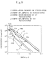
- FIGURE 23 is a graph showing the boron SIMS profiles of (a) a silicon substrate which has been implanted with BF 2 ions at an implant energy of 30 keV at a dosage of 2 ⁇ 10 15 cm -2 before being subjected to an activation annealing treatment at 1000 degrees centigrade for ten seconds and (b) a silicon substrate which has been implanted with B (boron) ions at an implant energy of 10 keV at a dosage of 2 ⁇ 10 15 cm -2 before being subjected to an activation annealing treatment at 1000 degrees centigrade for ten seconds.
- BF 2 Boron fluoride
- boron results from fluoride-boron bounding, which gives rise to dissociation, and there are created two impurity concentration peaks (see FIGURE 23). Although the higher of these two peaks is located on the side of the substrate surface, the boron will make no contribution to forming a final diffusion layer, for the boron is present in an area that is silicided later. As a result, the concentration at a silicide/diffusion layer interface decreases from the diffusion layer's original concentration peak, so that the contact resistance of this portion increases. Further, in the case of the surface channel type transistor, when implanting impurities into a diffusion layer, a gate electrode is also implanted with the impurities. Therefore, it becomes necessary to pay attention to the penetration phenomenon in which the impurities penetrate from the gate electrode towards the substrate through a gate insulation film.
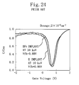
- FIGURE 24 shows the quasi-static C-V characteristic of the BF 2 (boron fluoride) implant (implant energy: 30 keV; dosage: 2 ⁇ 10 15 cm -2 ) and the B (boron) implant (implant energy: 10 keV; 2 ⁇ 10 15 cm -2 ).
- the waveform flat band voltage (Vfb) is 0.86 V.
- the Vfb is 0.88 V, from which it can be seen that somewhat penetration has occurred.
- FIGURE 25 shows the dependency of the implant dosage of boron and BF 2 upon the flat band voltage.
- the implant energy/dosage increases the shift of the flat band voltage likewise increases, and penetration becomes significant.
- a technique in which a greater implant energy and a greater dosage are used for the purpose of obtaining a greater impurity concentration at the interface between a post-silicide-formation silicide and a diffusion layer, is adopted, this accelerates impurity penetration from gate electrode towards substrate. As a result, it becomes hard to fabricate high-performance transistors.
- a second object of the present invention is directed to semiconductor elements which require the formation of shallow junctions. More specifically, diffusion is controlled or held low to create shallow junctions without increasing characteristic degradation and production costs, to provide high-performance devices with a microstructure.
- the present invention intends to form low-resistance silicide films and shallow junctions while holding boron penetration as low as possible.
- An oxynitride layer is formed at at least one edge of a gate oxide layer that is located on the drain side, thereby holding hot carrier degradation as low as possible and avoiding a drop in performance due to, for example, gate electrode depletion.
- Nitrogen is doped into an impurity diffusion layer in such a way as not to cause defects in excess of the level of detection due to collisions of nitrogen and semiconductor atoms, to provide an improved concentration profile for diffusion layers while at the same time preventing the occurrence of characteristic degradation by defects.
- the present invention provides a first semiconductor device, the first semiconductor device comprising:
- the oxynitride layer is formed only at one edge or both edges of the gate oxide film this prevents not only downward diffusion of the impurities present in the gate electrode but also transistor performance degradation duet to, for example, gate electrode depletion.
- Hot carrier degradation is caused by capture of hot carriers in a gate insulation film on the drain side.
- the oxynitride layer is formed, in an effective manner, in the drain-side gate oxide film which is a cause of the hot carrier degradation, so that hot carrier reliability can be improved.
- the oxynitride layer is formed at each edge of the gate oxide film in the first semiconductor device.
- the first semiconductor device further comprises a nitrogen diffusion layer which is formed in at least a portion of the drain region of the source and drain regions.
- the formation of the nitrogen diffusion layer in the semiconductor substrate prevents the occurrence of channeling at the ion implant time.
- This provides structures capable of forming source and drain regions with stability and the characteristic of transistor becomes stable.
- Impurity concentration particularly at a near-surface area of the semiconductor substrate, increases thereby reducing sheet resistance.
- the first semiconductor device further has on the gate electrode an over-gate insulation film which is patterned simultaneously with the gate electrode.
- the top of the gate electrode is protected by the over-gate insulation film at the time of forming the oxynitride layer by an impurity ion implant or by introducing or doping nitrogen into an edge of the gate oxide film through thermal diffusion, plasma nitriding or the like. This makes it possible to prevent transistor performance degradation due to, for example, gate electrode depletion without fail.
- the present invention provides a second semiconductor device which comprises:
- Such arrangement presents benefits, one of which is that, since diffusion of the first conductivity type impurity contained in the impurity diffusion layer is controlled by the existence of the doped nitrogen, this allows areas of the impurity diffusion layer heavily doped with the first conductivity type impurity to concentrate on a near-surface area of the substrate. As a result, the sheet resistance of the impurity diffusion layer is considerably reduced, and various semiconductor devices, which are superior in characteristic, can be accomplished using such low-sheet-resistance impurity diffusion layers. Additionally, such an impurity diffusion layer suffers much less deficiency therefore preventing the characteristic of semiconductor device from being affected.
- the first conductivity type impurity has, in the impurity diffusion layer, a concentration distribution profile in which:
- Such arrangement provides an ideal concentration profile for the first conductivity type impurity in the impurity diffusion layer, whereby the aforesaid effects can be produced significantly.
- the peak of impurity concentration is not located immediately under the substrate surface, but the impurity concentration peak is a little way off the substrate surface. Therefore, when the silicide film is formed the peak lies immediately under the silicide film. This considerably reduces the sheet resistance of the impurity diffusion layer and achieves a reduction of the junction leakage.
- an area of the source and drain regions, in which the concentration of the impurity for carrier generation is in excess of a predetermined value, is formed such that, at a portion thereof located adjacent to the channel region, the area more protrudes towards the channel region in a near-surface region of the semiconductor substrate while the area more sets back in the direction away from the channel region at a deeper region in the semiconductor substrate in comparison with a case in which nitrogen is absent.
- transistor parasitic resistance is reduced and resistance to punch-through is enhanced thereby providing an improved function of controlling short channel effects and reducing parasitic capacitance.
- a structure suitable for fast operation and miniaturization is obtained.
- the base region comes to have a steep impurity concentration distribution.
- the base region comes to have a reduced thickness. Accordingly, a reduction of the base resistance is achieved and bipolar transistors with a high cutoff frequency can be fabricated.
- the present invention provides a first method of fabricating a semiconductor device having a MIS-type field effect transistor, the first semiconductor device fabrication method comprising the steps of:
- the aforesaid first semiconductor device is fabricated.
- the nitrogen ions are implanted at a large angle of tilt and the oxynitride layer is formed only at the edge of the gate oxide film. Even if a weaker implant energy and a lower dosage, in comparison with nitrogen implantation to the entirety of a gate electrode, are employed, formation of an oxynitride layer capable of sufficiently controlling hot carrier degradation can be made, and no gate electrode depletion occurs. Additionally, the amount of nitrogen that is implanted into a semiconductor substrate can be reduced, whereby crystallinity disturbance in active regions is reduced as low as possible, and therefore reliable, high-performance transistors can be formed.
- an implant of impurity ions is performed in the fourth step in which the impurity ions are implanted from directions including at least two directions or more including a direction with a tilt towards the drain region and a direction with a tilt towards the source region.
- the oxynitride film is formed at each edge of the gate oxide film thereby making it possible to form transistors which suffer less hot carrier degradation.
- an implant of impurity ions is performed in the fourth step in which the impurity ions are implanted from a direction with a tilt angle of 10 degrees or more to a direction perpendicular to a surface of the semiconductor substrate in a cross section in parallel with the channel direction of the transistor.
- the fourth step may be carried out by subjecting the semiconductor substrate to an anneal in an ambient of gas including at least nitrogen, e.g., in an ambient of ammonia gas or by generating plasmas in an ambient of gas including nitrogen.
- nMIS-type field effect transistor is fabricated in the first active region, while in the second active region a pMIS-type field effect transistor, which is superior in mutual conductance, is fabricated because no oxynitride lay is formed.
- the first semiconductor device fabrication method further includes:
- a nitrogen diffusion layer is formed within the second active region, which prevents impurity ion channeling in the fifth step.
- the formation of the source and drain regions becomes stable.
- CMOS-type field effect transistors which suffer less gate electrode depletion and have greater drive power can be formed.
- the present invention provides a second semiconductor fabrication method.
- the second semiconductor device fabrication method comprises the steps of:
- the second semiconductor device fabrication method makes it possible to easily fabricate the second semiconductor devices. Note that the second step and the third step may be carried out in succession.
- the first step may be carried out by subjecting the semiconductor substrate to a thermal annealing treatment in an ambient of gas including at least nitrogen.
- the third step may be carried out in an ambient of ammonia gas.
- the third step is carried out at a temperature of 900 degrees centigrade or more for ten seconds or less.
- the first step may be carried out by generating plasmas in an ambient of gas including at least nitrogen.
- the second semiconductor device fabrication method may further include forming a silicide film over the source and drain regions after the third step is carried out.
- This method makes it possible to form bipolar transistors with a high cutoff frequency.
- FIGURES 1(a)-(d) are cross-sectional views illustrating process steps used in the fabrication of an nMOS field effect transistor in accordance with a first embodiment of the present invention.
- FIGURES 2(a)-(d) are cross-sectional views illustrating process steps used in the fabrication of an nMOS field effect transistor in accordance with a second embodiment of the present invention.
- FIGURES 3(a)-(d) are cross-sectional views illustrating process steps used in the fabrication of a CMOS device in accordance with a third embodiment of the present invention.
- FIGURES 4(a)-(d) are cross-sectional views illustrating process steps used in the fabrication of a CMOS device in accordance with a fourth embodiment of the present invention.
- FIGURES 5(a)-(e) are cross-sectional views illustrating process steps used in the fabrication of a CMOS device in accordance with a fifth embodiment of the present invention.
- FIGURES 6(a)-(e) are cross-sectional views illustrating process steps used in the fabrication of a CMOS device in accordance with a sixth embodiment of the present invention.
- FIGURES 7(a)-(c) are cross-sectional views illustrating process steps of the formation of an impurity diffusion layer in a seventh embodiment of the present invention.
- FIGURE 8 shows impurity concentration profiles of (a) a boron diffusion layer with nitrogen introduction, (b) a BF 2 diffusion layer with nitrogen introduction, (c) a boron diffusion layer without nitrogen introduction and (d) a BF 2 diffusion layer with nitrogen introduction.
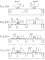
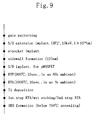
- FIGURE 9 is a flow diagram showing the fabrication of a pMOS field effect transistor in accordance with an eighth embodiment of the present invention.
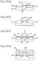
- FIGURES 10(a)-(d) are cross-sectional views illustrating process steps used in the fabrication of a pMOS field effect transistor of the eighth embodiment of the present invention.
- FIGURE 11 shows data about the dependency of threshold voltage upon gate length for understanding the effect of the eighth embodiment of the present invention.
- FIGURE 12 shows data about the characteristic of saturation current for understanding the effect of the eighth embodiment of the present invention.
- FIGURE 13 shows data about the dependency of contact resistance upon the area of silicided region interface for understanding the effect of the eighth embodiment of the present invention.
- FIGURE 14 shows data about the dependency of the gate resistance of transistor on the n channel side upon the gate width for understanding the effect of the eighth embodiment of the present invention.
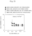
- FIGURE 15 shows data about the dependency of the sheet resistance upon the silicide width for understanding the effect of the eighth embodiment of the present invention.
- FIGURE 16 is a cross-sectional view useful for understanding the difference between a source/drain region of a pMOS field effect transistor of the eighth embodiment and a source/drain region of a conventional pMOS field effect transistor formed by boron implantation only.
- FIGURE 17 is a diagram useful for understanding the reason of why there is produced the difference between a source/drain region of a pMOS field effect transistor of the eighth embodiment and a source/drain region of a conventional pMOS field effect transistor formed by implanting only boron.
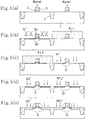
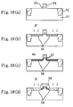
- FIGURES 18(a)-(d) are cross-sectional views illustrating process steps used in the fabrication of a pMOS field effect transistor in accordance with a ninth embodiment of the present invention.
- FIGURES 19(a)-(d) are cross-sectional views illustrating process steps used in the fabrication of a pMOS field effect transistor in accordance with a tenth embodiment of the present invention.
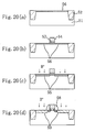
- FIGURES 20(a)-(d) are cross-sectional views illustrating process steps used in the fabrication of a pMOS field effect transistor in accordance with an eleventh embodiment of the present invention.
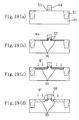
- FIGURES 21(a)-(c) are cross-sectional views illustrating process steps used in the fabrication of an npn bipolar transistor in accordance with a twelfth embodiment of the present invention.
- FIGURES 22(a)-(d) are cross-sectional views illustrating process steps employed in the fabrication of an nMOS field effect transistor in accordance with a prior art technique.
- FIGURE 23 shows concentration profiles for boron and BF 2 in a source/drain region of a conventional pMOS field effect transistor.
- FIGURE 24 shows the quasi static C-V characteristic of a conventional pMOS field effect transistor having a source/drain region formed by implantation of boron and BF 2 .
- FIGURE 25 is a diagram showing the dependency of the flat band voltage of conventional pMOS field effect transistor upon the dosage of boron and BF 2 .
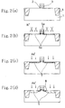
- FIGURES 1(a)-(d) are cross-sectional views illustrating process steps used in the fabrication of an nMOS field effect transistor in accordance with a first embodiment of the present invention.
- element isolator 4 is formed in a portion of silicon substrate 1 .
- a film of oxide is then formed by, for example, thermal oxidation on silicon substrate 1 in an active region surrounded by element isolator 4 , having a thickness of 7 nm.
- a polysilicon film is deposited overlying the oxide film, to a thickness of 150 nm. These films are patterned using photolithography and dry etching, to form gate oxide film 2 and gate electrode 3 .
- the polysilicon film has been doped with n-type impurities by ion implant at the time of or after depositing the same, to secure the conductivity of gate electrode 3 .
- a four-step ion implant is performed in which ions of nitrogen (N+) are implanted from directions with a tilt angle of 25 degrees to directions perpendicular to the silicon substrate surface in a cross section in parallel with the transistor channel direction, as indicated by arrows in the figure.
- the implant energy is 10 keV and the dosage is 1 ⁇ 10 15 cm -2 .
- the implant direction is fixed, and it is arranged such that silicon substrate 1 rotates on the horizontal by an angle of 90 degrees for four-position implantation.
- the nitrogen ions are diffused by an annealing treatment, whereby oxynitride layer 5a is formed at each edge of gate oxide film 2 and nitrogen diffusion layer 6a is formed in silicon substrate 1 .
- a preferred implant energy range for this nitrogen implant is 5-20 keV.
- the nitrogen ion implant is preferably performed at implant energies ranging from 5 keV to 20 keV at dosages ranging from 1 ⁇ 10 13 cm -2 to 5 ⁇ 10 15 cm -2 at tilted angles ranging from 7 degrees to 45 degrees.
- the present embodiment employs a four-step nitrogen ion implant so that the impurity ions are driven into both edges of gate oxide film 2 .
- impurity may simply be implanted from one direction with an inclination towards the drain region.
- the direction in which impurity ions are implanted does not necessarily correspond to the transistor channel direction (i.e., the direction in parallel with the FIG. 1 paper).
- the benefits of the present embodiment can be obtained as long as the angle, formed between (a) a line projected onto a surface at which the ion drive direction crosses with the gate width direction at right angles and (b) a line normal to the substrate surface, is 10 degrees or more. What is mentioned above applies in the other embodiments of the present invention.
- an arsenic (As+) ion implant is carried out from directions approximately perpendicular to silicon substrate 1 at an implant energy of 10 keV at a dosage of 1 ⁇ 10 15 cm -2 , to form lightly-doped (low concentration) n-type source/drain region 7 at a near-surface area of silicon substrate 1 .
- the formation of nitrogen diffusion layer 6a in silicon substrate 1 prevents the occurrence of channelling, even when impurity ions are implanted vertically.
- a relatively thick silicon oxide film is deposited on the substrate. Subsequently, the silicon oxide film is etched back, to form sidewall 8 on each side surface of gate electrode 3 .
- An approximately vertical ion implant is performed in which arsenic ions (As+) are implanted at an implant energy of 30 keV at a dosage of 5 ⁇ 10 15 cm -2 , to form heavily-doped (high-concentration) n-type source/drain region 9 on one side of each sidewall 8 .
- nMOS field effect transistor fabricated in accordance with the fabrication process steps of the present embodiment, differs in structure from a conventional transistor having an oxynitride layer. More specifically, in the present nMOS field effect transistor, oxynitride layer 5a is formed only at both edges of gate oxide film 2 . A major cause of hot carrier degradation exists in the fact that hot carriers are captured in a gate oxide film on the drain side. Accordingly, the formation of oxynitride layer 5a at at least one of the edges of gate oxide film 2 (oxynitride is formed at each edge of gate oxide film 2 in the present embodiment), prevents the occurrence of hot carrier degradation.
- oxynitride layer 5a it is sufficient to implant nitrogen ions, only into an edge of gate oxide film 2 by a large-tilted-angle implant, thereby making it possible to form oxynitride layer 5a by a nitrogen ion implant in which ions of nitrogen are implanted at a low implant energy of 10 keV at a low dosage of approximately 1 ⁇ 10 15 cm -2 .
- the dosage of nitrogen must be increased and, as a result, gate electrode depletion occurs.
- the nitrogen dosage can be held very low, thereby preventing the occurrence of gate electrode depletion.
- nitrogen diffusion layer 6a is formed in silicon substrate 1 in the process step of FIGURE 1(b), not to a great depth, so that crystallinity disturbance occurs only in limited areas. Further, since the concentration of nitrogen in nitrogen diffusion layer 6a is also low, this can retain the degree of disturbance in crystallinity in the silicon substrate 1 to a minimum. Accordingly, degradation in transistor performance can be held low and transistor reliability can be improved.
- oxynitride layer 5a is formed at each edge of gate oxide film 2 .
- FIGURES 2(a)-(d) are cross-sectional views illustrating process steps used in fabricating an nMOS field effect transistor in accordance with a second embodiment of the present invention.
- element isolator 4 is formed in a portion of silicon substrate 1 .
- a film of oxide is then formed by, for example, thermal oxidation at silicon substrate 1 within an active region surrounded by element isolator 4 , this oxide film having a thickness of 7 nm.
- This is followed by deposition of a 150-nm thick polysilicon film and a 150-nm thick oxide film on the aforesaid 7-nm thick oxide film.
- These three films are patterned using photolithography and dry etching, to form gate oxide film 2 , gate electrode 3 and over-gate oxide film 10 .
- a four-step ion implant is carried out in which ions of nitrogen (N+) are implanted from directions with a tilt angle of 25 degrees to directions perpendicular or normal to the substrate surface, as indicated by arrows in the figure.
- the implant energy is 10 keV and the dosage is 1 ⁇ 10 15 cm -2 .
- the implant direction is fixed, and it is arranged such that silicon substrate 1 rotates on the horizontal by 90 degrees for four-position implantation.
- the nitrogen ions are diffused by a thermal annealing treatment to form oxynitride layer 5a at each edge of gate oxide film 2 as well as to form nitrogen diffused layer 6a in silicon substrate 1 .
- the preferable implant energy ranges from 5 keV to 30 keV
- the preferable dosage ranges from 1 ⁇ 10 13 cm -2 to 5 ⁇ 10 16 cm -2
- the preferable angle of tilt ranges from 7 degrees to 45 degrees.
- an ion implant is carried out in which ions of arsenic (As+) are implanted from the direction approximately perpendicular to the surface of silicon substrate 1 at an implant energy of 10 keV at a dosage of 1 ⁇ 10 14 cm -2 , to form lightly-doped (low-concentration) n-type source/drain region 7 in a near-surface area of silicon substrate 1 .
- ions of arsenic (As+) are implanted from the direction approximately perpendicular to the surface of silicon substrate 1 at an implant energy of 10 keV at a dosage of 1 ⁇ 10 14 cm -2 , to form lightly-doped (low-concentration) n-type source/drain region 7 in a near-surface area of silicon substrate 1 .
- a rather thick silicon oxide film is deposited overlying the substrate surface.
- the silicon oxide film deposited is then etched back, to form sidewall 8 on each side surface of gate electrode 3 .
- This is followed by an ion implant in which ions of arsenic (As+) are implanted at approximately right angles to the substrate surface at an implant energy of 30 keV with a dosage of 5 ⁇ 10 15 cm -2 , whereby heavily-doped (high-concentration) n-type source/drain region 9 is formed on one side of each sidewall 8 .
- the present embodiment provides the following effect.
- over-gate oxide film 10 is formed on gate electrode 3 , so that the quantity of nitrogen which is implanted into gate electrode 3 in the process step of FIGURE 2(b) can be considerably reduced. This enables the control of transistor characteristic degradation due to depletion of gate electrode 3 . Additionally, even if the implant energy and dosage of nitrogen is increased, this will not cause gate electrode 3 to deplete and it becomes possible to widen the range of selection for requirements.
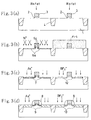
- FIGURES 3(a)-(d) are cross-sectional views of process steps used in the fabrication of a CMOS device in accordance with a third embodiment of the present invention.
- element isolator 4 is formed in silicon substrate 1 for isolation between an nMOSFET formation region Rnfet (a first active region) and a pMOSFET formation region Rpfet (a second active region).
- a film of oxide is then formed by, for example, thermal oxidation on silicon substrate 1 within each region Rnfet and Rpfet surrounded by element isolator 4 , this oxide film having a thickness of 7 nm.
- a film of polysilicon is deposited on the oxide film to a thickness of 150 nm.
- Both the oxide film and the polysilicon film are patterned by photolithography and dry etching, to form gate oxide film 2 and gate electrode 3 in each region Rnfet and Rpfet.
- the polysilicon film on region Rnfet is n-doped and the polysilicon film on region Rpfet is p-doped at or after the deposition by CVD (chemical vapor deposition), not only in the present embodiment but also in the following embodiments (the fourth to sixth embodiments of the present invention).
- a film of photoresist Fr1 is applied covering region Rpfet (the pMOSFET formation region).
- photoresist film Fr1 serving as a mask, a four-step ion implant is performed in which ions of nitrogen (N+) are implanted at an implant energy of 10 keV at a dosage of 1 ⁇ 10 15 cm -2 , at an angle of tilt of 25 degrees to the direction perpendicular to the surface of silicon substrate 1 .
- an ion implant is carried out on region Rnfet in which ions of arsenic (As+) are implanted at an implant energy of 10 keV at a dosage of 1 ⁇ 10 14 cm -2 at approximately right angles to the substrate surface, to form lightly-doped n-type source/drain region 7
- an ion implant is carried out on region Rpfet in which ions of boron fluoride (BF 2 +) are implanted at an implant energy of 10 keV at a dosage of 1 ⁇ 10 14 cm -2 at approximately right angles to the substrate surface, to form lightly-doped p-type source/drain region 12 .
- BF 2 + boron fluoride
- an ion implant is performed into region Rnfet in which ions of arsenic (As+) are implanted at an implant energy of 30 keV at a dosage of 5 ⁇ 10 15 cm -2 at approximately right angles to the substrate surface, to form heavily-doped n-type source/drain region 9 on one side of each sidewall 8 as shown in the figure.
- ions of arsenic (As+) are implanted at an implant energy of 30 keV at a dosage of 5 ⁇ 10 15 cm -2 at approximately right angles to the substrate surface, to form heavily-doped n-type source/drain region 9 on one side of each sidewall 8 as shown in the figure.
- an ion implant is performed into region Rpfet in which ions of boron fluoride (BF2+) are implanted at an implant energy of 30 keV at a dosage of 5 ⁇ 10 15 cm -2 at approximately right angles to the substrate surface, to form heavily-doped n-type source/drain region 13 on one side of each sidewall 8 as shown in the figure.
- ions of boron fluoride BF2+
- the present embodiment provides, in addition to the effects of the third embodiment, an effect of controlling the degradation of mutual conductance in the pMOS field effect transistor.
- FIGURES 4(a)-(d) are cross-sectional views depicting process steps used in the fabrication of a CMOS device in accordance with a fourth embodiment of the present invention.
- Such arrangement allows the present embodiment to provide, in addition to the aforementioned effects of the third embodiment, anther effect of achieving considerable reduction of the quantity of nitrogen being implanted into gate electrode 3 because of the provision of over-gate oxide film 10 on gate electrode 3 , therefore ensuring that transistor performance degradation due to the depleting of gate electrode 3 is prevented.
- FIGURES 5(a)-(e) are cross-sectional views depicting process steps used in the fabrication of a CMOS device in accordance with a fifth embodiment of the present invention.
- element isolator 4 is formed in a porion of silicon substrate 1 .
- a film of oxide is formed by, for example, thermal oxidation, on silicon substrate 1 within an active region surrounded by element isolator 4 , the oxide film having a thickness of 7 nm.
- a film of polysilicon is deposited on the oxide film to a thickness of 150 nm.
- the oxide film and the polysilicon film are patterned using photolithography and dry etching, to form gate oxide film 2 and gate electrode 3 in region Rnfet (the nMOSFET formation region) as well as in region Rpfe (the pMOSFET formation region).
- a film of photoresist Fr1 is applied covering region Rpfet.
- photoresist film Fr1 serving as a mask, a four-step ion implant is carried out in which ions of nitrogen (N+) are implanted at an implant energy of 10 keV at a dosage of 1 ⁇ 10 15 cm -2 , at an angle of tilt of 25 degrees to the direction perpendicular to the surface of silicon substrate 1 .
- the nitrogen ions thus implanted are diffused by a thermal annealing treatment, to form oxynitride film 5a at each edge of gate oxide film 2 of region Rnfet as well as to form nitrogen diffusion layer 6a in silicon substrate 1 .
- a film of photoresist Fr2 is applied covering region Rnfet.
- photoresist film Fr2 serving as a mask, an ion implant is carried out in which ions of nitrogen (N+) are implanted at an implant energy of 10 keV at a dosage of 1 ⁇ 10 15 cm -2 , at approximately right angles to the substrate surface.
- the nitrogen ions implanted are diffused by a thermal annealing treatment, to form nitrogen diffuses layer 6 in silicon substrate 1 of region Rpfet.
- Weak oxynitride layer 5 is formed in gate oxide film 2 .
- regions Rnfet and Rpfet are formed on regions Rnfet and Rpfet (not shown in the figure), and lightly-doped source/drain regions 7 and 12 are formed in the region Rnfet and in the region Rpfet, respectively. More specifically, an ion implant is performed into region Rnfet in which ions of arsenic (As+) are implanted at an implant energy of 10 keV at a dosage of 1 ⁇ 10 14 cm -2 at approximately right angles to the substrate surface, to form lightly-doped n-type source/drain region 7 .
- ions of arsenic (As+) are implanted at an implant energy of 10 keV at a dosage of 1 ⁇ 10 14 cm -2 at approximately right angles to the substrate surface, to form lightly-doped n-type source/drain region 7 .
- an ion implant is performed into region Rpfet in which ions of boron fluoride (BF 2 +) are implanted at an implant energy of 10 keV at a dosage of 1 ⁇ 10 14 cm -2 at approximately right angles to the substrate surface, to form lightly-doped p-type source/drain regions 12 .
- ions of boron fluoride BF 2 +
- an ion implant is performed into region Rnfet in which ions of arsenic (As+) are implanted at an implant energy of 30 keV at a dosage of 5 ⁇ 10 15 cm -2 at approximately right angles to the substrate surface, to form heavily-doped n-type source/drain regions 9 on one side of each sidewall 8 as shown in the figure.
- ions of arsenic (As+) are implanted at an implant energy of 30 keV at a dosage of 5 ⁇ 10 15 cm -2 at approximately right angles to the substrate surface, to form heavily-doped n-type source/drain regions 9 on one side of each sidewall 8 as shown in the figure.
- an ion implant is performed into region Rpfet in which ions of boron fluoride (BF 2 +) are implanted at an implant energy of 30 keV at a dosage of 5 ⁇ 10 15 cm -2 at approximately right angles to the substrate surface, to form heavily-doped p-type source/drain regions 13 on one side of each sidewall 8 as shown in the figure.
- ions of boron fluoride BF 2 +
- CMOS devices fabricated in accordance with the present embodiment, are approximately identical in structure with ones formed in accordance with the third embodiment.
- nitrogen diffusion layer 6 is formed within silicon substrate 1 of the pMOS field effect transistor. Such formation provides, in addition to the effects of the third embodiment, another effect of preventing channelling from occurring in region Rpfet at the time of implanting impurity ions, and the stable formation of source/drain regions can be achieved.
- Nitrogen is implanted at approximately right angles to the substrate surface, as a result of which an oxynitride layer is slightly formed in gate electrode 3 of gate oxide film 2 , whereby boron penetration from gate electrode 3 towards silicon substrate 1 can be held as low as possible in the pMOS field effect transistor.
- FIGURES 6(a)-(e) are cross-sectional views illustrating process steps used in the fabrication of a CMOS device in accordance with a sixth embodiment of the present invention.
- CMOS device fabrication of the present embodiment is almost the same as the CMOS device fabrication of the fifth embodiment.
- over-gate oxide film 10 is formed on gate electrode 3 in the FIG. 6(a) process step.
- the CMOS device of the present embodiment provides an effect of considerably reducing the quantity of nitrogen that is implanted into gate electrode 3 , in addition to the effects of the fifth embodiment, thereby further ensuring that degradation in transistor characteristic due to the depleting of gate electrode 3 is prevented.
- FIGURE 7, comprised of 7(a)-(c), shows the fabrication of a semiconductor device of a seventh embodiment of the present invention.
- process steps for improving the distribution of impurity concentration in p-type diffusion layer will be described below.
- an ion implant is carried out to n-type silicon substrate 21 in which ions of boron (B+) are implanted at an implant energy of 10 keV at a dosage of 2 ⁇ 10 15 cm -2 .
- an ion implant may be performed in which ions of BF 2 are implanted at an implant energy of 30 keV at a dosage of 2 ⁇ 10 15 cm -2 .
- Such boron or BF 2 doping forms p-type diffusion layer 22 which will be later subjected to an activation treatment.
- silicon substrate 21 is placed in a commonly-used rapid thermal annealing apparatus, and a rapid thermal annealing treatment is carried out at 900 degrees centigrade for ten seconds in an ambient of ammonia gas at a flow rate of 5 lit. per minute.
- a rapid thermal annealing treatment is carried out at 900 degrees centigrade for ten seconds in an ambient of ammonia gas at a flow rate of 5 lit. per minute.
- nitrogen is introduced into silicon substrate 21 , and boron/nitrogen mixture layer 23 (nitrogen diffusion layer) is formed in areas from the surface of silicon substrate 21 down to a predetermined depth.
- a thermal annealing treatment is performed by rapid thermal annealing apparatus at 1000 degrees centigrade for ten seconds, and, as a result, the boron or BF 2 in p-type diffusion layer 22 is activated and diffused.
- the range of p-type diffusion layer 22 is defined. The nitrogen becomes diffused together with the boron (or BF 2 ).
- FIGURE 8 shows concentration profiles in the direction of depth, for boron and BF 2 (concentration distribution curves L1 and L2), and nitrogen (a concentration distribution curve Ln) in p-type diffusion layer 22 of the present embodiment.
- concentration distribution curves L3 and L4 for boron and BF 2 with thermal annealing for activation but without rapid thermal annealing in an ambient of ammonia gas are shown.
- SAMPLE-a, SAMPLE-b, SAMPLE-c and SAMPLE-d are used as examples.
- SAMPLE-a is a p-type diffusion layer of the present embodiment, in other words SAMPLE-a is a source/drain region which has undergone a rapid thermal annealing treatment in an ambient of ammonia gas after a boron implant.
- SAMPLE-b is a p-type diffusion layer which has undergone a rapid thermal annealing treatment in an ambient of ammonia gas after a BF 2 implant at an implant energy of 30 keV.
- SAMPLE-c is a p-type diffusion layer which has undergone no rapid thermal annealing treatment in an ambient of ammonia gas after a boron implant at an implant energy of 10 keV.
- SAMPLE-d is a p-type diffusion layer which has undergone no rapid thermal annealing treatment in an ambient of ammonia gas after a BF 2 implant at an implant energy of 30 keV.
- the reason of why boron and BF 2 are implanted at different levels of implant energy is to give compensation for the difference in implant depth caused by the difference in mass.
- SAMPLE-a which has undergone a rapid thermal annealing treatment in an ammonia gas ambient after implantation of boron and doping of nitrogen, has the feature that, since an area of the original impurity diffusion layer 22 down to a depth of approximately 0.1 ⁇ m becomes boron/nitrogen mixture layer 23 , the concentration of boron in boron/nitrogen mixture layer 23 is high.
- SAMPLE-c (L3) which has undergone no nitrogen doping, the boron concentration of SAMPLE-a rapidly decreases after passing through a peak point Peb (a region L1a in the figure).
- the decreasing rate drops in the vicinity of a point Pch1 and thereafter the boron concentration of SAMPLE-a decreases at a relatively gentle rate, so that the boron concentration of SAMPLE-a approaches to that of SAMPLE-c (a region L1b in the figure).
- the point Pch is an inflection point of concentration when the concentration is a function of the depth.
- boron diffusion is held low by boron present in boron/nitrogen mixture layer 23 , and the boron, after the activation, tends to intensively exist or concentrate in an area, the nitrogen concentration of which is high, located above an approximately 0.1- ⁇ m depth.
- the doping of nitrogen into semiconductor substrates has been proposed in the art.
- ions of nitrogen are doped.
- a nitrogen ambient such as in an ammonia gas ambient.
- the present embodiment makes it possible to form a relatively heavily-doped nitrogen diffusion layer in a silicon substrate by carrying out a rapid thermal annealing treatment at a relatively high temperature in an ammonia gas ambient.
- the present embodiment employs nitrogen doping by thermal annealing so that no defects occur to silicon substrates. It is understood that impurity diffusion is not controlled by defects created at the time of doping of nitrogen.
- L4 which is the concentration distribution curve of SAMPLE-d which has undergone an activation process with BF 2 introduction but without nitrogen doping, has a peak in the value in immediate proximity to the surface. After the value peak, L4 gently decreases and the peak value is small. The reason for this may be that the diffusion of BF 2 is overall controlled by the presence of fluorine.
- the impurity concentration profile of the present embodiment cannot be obtained by BF 2 implantation only. of the present embodiment cannot be obtained by BF 2 implantation only.
- L2 which is the concentration distribution curve of SAMPLE-b which has undergone a rapid thermal annealing treatment in an ambient of ammonia gas after introduction of BF 2 and N, has an inflection point Pch2 at a depth of approximately 0.07 ⁇ m ( ⁇ 0.1 ⁇ m). This allows heavily-doped areas to concentrate in a much smaller range.
- FIGURE 8 shows various concentration profiles obtained by performing, under particular conditions, nitrogen implantation and rapid thermal annealing treatment in an ambient of ammonia gas.
- the temperature and time of rapid thermal annealing treatment may be adjusted, or the step of implanting boron and the step of performing rapid thermal annealing treatment may be carried out in a different order, to control the profile of boron concentration.
- the rapid thermal annealing treatment be performed at a temperature of 900 degrees centigrade or more for 10 seconds or more, for generally ammonia gas pylolytically decomposes at above 800 degrees centigrade and becomes activated at above 900 degrees centigrade.
- the annealing treatment is case of nMOS transistors.
- the ammonia flow rate is from about 1 to about 10 slm, which, however, is not to be considered restrictive.
- the concentration distribution in the vicinity of the surface shown by LI of FIGURE 8 becomes further steeper by performing a pulse-like thermal annealing treatment for a considerably short period of time (for example, cooling starts as soon as a target temperature is reached).
- a pulse-like thermal annealing treatment for a considerably short period of time (for example, cooling starts as soon as a target temperature is reached).
- the peak value Peb further increases and the inflection point Pch1 shifts to the left.
- the step of performing a rapid thermal annealing treatment in an ambient of ammonia gas and the step of performing a thermal annealing treatment for impurity activation may be carried out by a single annealing treatment.
- these two thermal annealing treatments may be carried out continuously as multi-stage processing.
- impurities for carrier generation which are introduced into semiconductor substrates
- phosphorus, arsenic, indium and antimony may be used in addition to boron.
- the doping of nitrogen produces the effect that not only the diffusion of carrier generation impurities but also the diffusion of impurities (i.e., fluorine) which do not generate carriers can be controlled. In other words, there is produced an effect of creating an inflection point in a concentration profile curve thereof.
- rapid thermal annealing which is performed in an ambient of gas resulting from adding to ammonia gas an inert gas such as nitrogen gas and argon gas, provides the same effects that the present embodiment does.
- a rapid thermal anneal which is carried out in an ambient of mixed gas of nitrogen and, for example, hydrogen or in an ambient of NF 3 gas, provides the same effects as in the present embodiment.
- the semiconductor region of the present invention may be a polycrystalline semiconductor region or an amorphous semiconductor region such a polysilicon region, in addition to the monocrystalline semiconductor region.
- impurities for carrier generation such as boron, phosphorous and arsenic may be introduced into polycrystalline or amorphous regions.
- the same impurity concentration profile as obtained in the present embodiment can be created by doping nitrogen into the regions.
- FIGURE 9 is a flow diagram showing the flow of the fabrication of a pMOS device of the present embodiment.
- FIGURES 10(a)-(d) are cross-sectional views illustrating process steps used in the fabrication of a pMOS device according to the present embodiment.
- n-type well 31 is formed in a silicon substrate.
- a film of oxide is then formed overlying n-type well 31 , having a thickness of approximately 4 nm.
- a film of polysilicon is formed on gate oxide film 32 , having a thickness of approximately 200 nm.
- the oxide and polysilicon films are patterned using lithography and RIE (reactive ion etching), to form gate oxide film 32 and gate electrode 33 .
- an ion implant is carried out in which ions of BF 2 are implanted at an implant energy of about 10 keV at a dosage of about 1 ⁇ 10 14 cm -2 , to form source/drain extension 34 (p-type diffusion layer). Further, still using gate electrode 33 as a mask, an ion implant is performed in which ions of arsenic are implanted at an implant energy of about 160 keV at a dosage of about 6 ⁇ 10 12 cm -2 at an angle of tilt of about 20 degrees, to form pocket 35 (n-type diffusion layer) for the purpose of providing an improved punch-through breakdown voltage.
- a film of oxide is deposited by LPCVD using TEOS gas, to a thickness of 120 nm. Subsequently, this oxide film is etched back by dry etching such that portions of the oxide film remain on both sides of gate electrode 33 , whereby sidewall 36 is formed on each side surface of the gate electrode 33 .
- This is followed by an ion implant in which ions of boron are implanted at an implant energy of about 10 keV at a dosage of about 2 ⁇ 10 15 cm -2 , to form source/drain region 37 (p-type diffusion layer). At this time, boron is introduced also into the gate, as a result of which an electrode for a p-type transistor is formed.
- the silicon substrate is placed in a commonly-used rapid thermal annealing apparatus, and an annealing treatment is carried out at 900 degrees centigrade for ten seconds in an ammonia gas ambient produced by ammonia gas at a flow rate of 5 lit. per minute.
- an annealing treatment is carried out at 900 degrees centigrade for ten seconds in an ammonia gas ambient produced by ammonia gas at a flow rate of 5 lit. per minute.
- nitrogen is doped into the silicon substrate, and boron/nitrogen mixture layer 38 (nitrogen diffusion layer) is formed at a near-surface area of source/drain region 37 .
- an annealing treatment as an annealing treatment for impurity activation, is carried out at a temperature of about 1000 degrees centigrade for about ten seconds in the rapid thermal annealing apparatus, to define the range of p-type extension 34 , p-type source/drain region 37 and n-type pocket 35 .
- nitrogen is diffused in source/drain region 37 to a depth of about 0.1 ⁇ m at a high concentration. Therefore, the boron concentration profile of source/drain region 37 approximately corresponds to the profile of FIGURE 8, in other words source/drain region 37 has such a concentration profile that high boron concentration areas concentrate in the vicinity of the surface.
- the diffusion of impurities is held low by nitrogen, also in extension 34 , so that relatively high-concentration boron exists in a near-surface area of extension 34 , and an area, located immediately underneath the aforesaid high-concentration area, has a concentration profile showing a steep concentration gradient (concentration drop).
- impurities for the formation of extension 34 and pocket region 35 are introduced also into source/drain region 37 , the presence of the introduced impurities in source/drain region 37 can be safely ignored, for the dosage used in the formation of extension 34 and pocket 35 is very small as compared with the dosage used in the formation of source/drain region 37 .
- the presence may affect the geometric form of source/drain region 37 , which is described later.
- a metal with a high melting point such as titanium (Ti) is deposited by sputtering, to a thickness of 30 nm and is then subjected to an annealing treatment at a temperature of 700 degrees centigrade for one minute.
- an annealing treatment As a result of such an annealing treatment, a near-surface area of source/drain region 37 formed of silicon, a near-surface area of gate electrode 33 formed of polysilicon, and other near-surface areas are brought to react with Ti, to form layers 39 of titanium silicide in these near-surface areas.
- Ti films, which are not silicided and remain not reacted, are stripped by wet etching.
- interlayer dielectric 40 buried plug 41 to a contact hole, interconnect lines (not shown in the figure) on the substrate, to fabricate a surface channel type pMOSFET.
- the high-concentration area of source/drain region 37 and the relatively high-concentration area of extension 34 concentrate in the vicinity of the surface, thereby providing an improved punch-through breakdown voltage as well as an improved short channel effect controlling function, as will be described later in detail.
- SAMPLE-A is a p-type MOSFET of the present embodiment, in other words SAMPLE-A has a source/drain region which has undergone a rapid thermal annealing treatment in an ambient of ammonia gas after an implant of boron
- SAMPLE-B is a p-type MOSFET which has undergone a rapid thermal annealing treatment in an ambient of ammonia gas after an implant of BF 2 at an implant energy of 30 keV
- SAMPLE-C is a p-type MOSFET which has undergone no rapid thermal annealing treatment in an ambient of ammonia gas after an implant of boron at an implant energy of 10 keV
- SAMPLE-D is a p-type MOSFET which has undergone no rapid thermal annealing treatment after an implant of BF 2 at an implant energy of 30 keV.
- FIGURE 11 is a characteristic diagram showing dependency of the threshold voltage of SAMPLE-A, SAMPLE-C and SAMPLE-D upon the gate length.
- FIGURE 11 shows that as the degree of variation in threshold voltage according to the gate length decreases the ability to control the short channel effect is enhanced.
- SAMPLE-A and SAMPLE-D were formed in such a way as to have approximately the same gate length and threshold voltage and their transistor characteristics (I-V characteristics) were measured.
- FIGURE 12 shows the measurement results.
- SAMPLE-A, SAMPLE-B, SAMPLE-C and SAMPLE-D were formed such that each sample has a film of silicide over its source/drain region.
- FIGURE 13 shows the variation in contact resistance of the silicide film/source/drain region interface for the area of the interface.
- FIGURE 11 shows that SAMPLE-A of the present embodiment, which has undergone a rapid thermal annealing treatment in an ambient of ammonia gas, provides an improved function of controlling short-channel effects as compared with SAMPLE-C which has undergone no rapid thermal annealing treatment in an ambient of ammonia gas.
- FIGURE 11 further shows that SAMPLE-A has approximately the same short-channel effect controlling function as SAMPLE-D which has undergone no rapid thermal annealing treatment after an implant of BF 2 ions at 30 keV.
- SAMPLE-A is compared in transistor characteristic with SAMPLE-D , and, as can be seen from FIGURE 12, the saturation drain current of SAMPLE-A is greater than that of SAMPLE-D by 15%, the reason for which may be explained as follows.
- SAMPLE-A has a lower silicide film/source/drain region interface resistance than SAMPLE-D (see FIGURE 13).
- the source/drain region resistance of SAMPLE-A is low because the skirt of the source/drain region profile is broadened by the boron 10-kev implant (in other words the impurity concentration of deep areas of the source/drain region of SAMPLE-A is high).
- the present MOS device although its short-channel controlling function is the same as that of the aforesaid MOS device, is able to provide a greater saturation drain current.
- FIGURE 14 an n-type MOSFET which has undergone a rapid thermal anneal after arsenic implantation and an n-type MOSFET which has undergone no rapid thermal anneal after arsenic implantation, are compared in dependency of the n-ch gate resistance upon the gate width.
- FIGURE 15 shows the dependency of the sheet resistance of the source/drain region of each sample (p-type MOSFET) upon the silicide width.
- the present embodiment's nitrogen doping produces no obstacles which prevent the aim of silicide technology (i.e., the achievement of lower resistance). Generally, it has been pointed out that nitrogen doping obstructs silicidation.
- the concentration of nitrogen used in the present embodiment is low enough to be negligible, therefore producing no obstacles to silicidation processing. Further, as can be seen from FIGURE 15, the unwanted sheet resistance increase is relaxed by the nitrogen doping. It has been known in the art that BF 2 ion doping creates an impurity concentration peak value in the close vicinity of the surface, which produces the problem that silicide films are not formed in uniform fashion. On the other hand, boron doping creates a peak value slightly below the surface (immediately under an area that is silicided), so that uniform silicide film formation is not disturbed. Additionally, in the MOS device of the present embodiment, the impurity concentration of areas located immediately under a silicide film which plays the most important role for reduction of the sheet resistance, is increased. As a result, considerable reduction of the sheet resistance can be achieved.
- the present embodiment is able to reduce junction leakage.
- FIGURE 16 is a cross-sectional view illustrating a structure in the vicinity of typical source/drain and channel regions of a MOSFET. In the figure, only the drain region is shown and the source region is not shown since the source region generally has a symmetrical structure with the drain region.
- FIGURE 17 is a graphical diagram about L1 and L3 of FIGURE 8.
- the curve L1 shows the concentration distribution of a source/drain region of the present embodiment implanted with both boron and nitrogen, for the substrate depth direction.
- the curve L3 shows the concentration distribution of a conventional source/drain region implanted with only boron with respect to the substrate depth direction.
- a conventional source/drain region SDb by boron implantation generally has a form indicated by broken line, which is explained as follows.
- impurity diffusion including diffusion by ion implantation and diffusion by annealing uniformly proceeds from the diffusion source at constant speed in each direction.
- the source/drain region surface is a source where diffusion begins, so that in the FIG. 16 cross-section diffusion starts from a linear diffusion source.
- a source/drain region SDbn of the present embodiment has a form indicated by solid line in the figure.
- the source/drain region can be divided roughly into three regions, namely a region Rch located adjacent to the channel region, a region Rpa which becomes a direction in which punch-through occurs and a region Rsb which is a bottom region located next to the substrate region.
- the semiconductor substrate is doped with n-type impurities such as arsenic and phosphorus for the control of threshold voltage as well as with n-type impurities for the prevention of punch-through. These heavily-doped n-type regions are located in a range of the semiconductor substrate at a particular depth from the substrate surface (see FIGURE 17).
- the source/drain region SDbn of the present embodiment therefore has the following geometric features over the conventional source/drain region SDb.
- the impurity concentration of source/drain region SDbn is higher than that of source/drain region SDb in the region Rch near the substrate surface, so that the source/drain region SDbn more protrudes towards the channel region than the source/drain region SDb.
- Heavily-doped area can be limited to exist in a narrow range in the vicinity of the substrate surface, which makes it possible to perform an implant of impurity ions for formation of a source/drain region at a greater implant energy than in a case in which nitrogen is not doped.
- the impurity concentration of the source/drain region SDb rapidly drops after the peak value, the effect of reduction of the carrier formation by n-type impurities is enhanced particularly in the region Rpa located at a greater depth than the channel region. Therefore, the region Rpa is more set back in the direction away from the channel region in comparison with the conventional MOSFET's source/drain region SDb. Further, as described above, because of the ability to perform an ion implant at an implant energy of greater level, the bottom region Rsb is located at a greater depth than the source/drain region SDb with no nitrogen doping. In other words, the concentration distribution of the source/drain region SDbn at deep areas of the substrate shows a broad distribution as compared with one without nitrogen doping. The source/drain region SDbn deepens accordingly.
- the present embodiment provides MOSFETs which have the following operational advantages.
- One of these advantages is that the protrusion of the region Rch in the vicinity of the substrate surface produces reduced parasitic capacitance.
- the region Rpa immediately below the region Rch is set back, whereby resistance to punch-through is enhanced and the ability to control the short-channel effect increases. Further, the region Rpa has a gentle inclination and parasitic capacitance is reduced.
- the pocket is not explained.
- the presence of the pocket contributes to the setting back of the region Rpa (FIGURE 16).
- the fabrication may be simplified by omitting the steps of forming a pocket.
- Ti self-aligned-silicidation processing is described as a means for achieving low resistance.
- the same effects as obtained in the Ti self-aligned-silicidation can be expected using other self-aligned-silicidation such as Co self-aligned-silicidation and Ni self-aligned-silicidation or by other ways such as tungsten bonding by selective tungsten deposition.
- the diffusion layer may be formed by the implanting of various impurities other than boron, such as phosphorus, arsenic, indium and antimony. This applies in controlling the diffusion of impurity such as fluorine which does not form a diffusion layer.
- Rapid thermal annealing in an ambient of, for example, nitrogen or argon may provide the same effects as obtained by rapid thermal annealing in an ambient of ammonia gas. It is deemed preferable to dope, as a second impurity, nitrogen separately from boron.
- Doping nitrogen into a source/drain region or into an extension of a source/drain region has been described.
- Doping nitrogen into a well or into a channel region also provides an effect of controlling the diffusion of impurities for carrier formation, as in the present embodiment.
- FIGURES 18(a)-(d) are cross-sectional views showing process steps used in the fabrication of a MOSFET of a ninth embodiment of the present invention.
- element isolator 52 is formed in a portion of silicon substrate 51 .
- Gate oxide film 53 and gate electrode 54 are formed overlying an active region surrounded by element isolator 52 .
- Gate oxide film 53 and gate electrode 54 are formed under the same formation conditions as used in each of the foregoing embodiments.
- extension 55 is formed under the same formation conditions as used in the eighth embodiment.
- an anneal is performed in an ambient of ammonia gas, to dope nitrogen ions into the silicon substrate.
- the processing time is shortened or the processing temperature is lowered, in order that high-concentration nitrogen is doped into shallower areas than the ones implanted with nitrogen in the eighth embodiment.
- nitrogen diffusion layer 56 is formed at a near-surface area of extension region 55 .
- oxynitride layer 57 is formed at each edge of gate oxide film 53 .
- sidewall 58 is formed on each side surface of gate electrode 54 . This is followed by a boron implant into the silicon substrate to form source/drain region 59 under the same formation conditions as used in the eighth embodiment.
- An annealing treatment is carried out for impurity activation, whereby extension 55 and source/drain region 59 are defined.
- steps of forming a film of silicide over the source/drain region and over the gate electrode are performed.
- the formation of such a silicide film may be omitted.
- relatively heavily-doped areas of extension 55 exist only on the surface region, thereby making it possible to form a shallow pn junction in the channel region and channel resistance is reduced.
- oxynitride layer 57 is formed at each edge of the gate oxide film, which, as in the first embodiment, provides improved reliability.
- the formation of a silicide film over the source/drain region makes it possible to considerably reduce contact resistance, as in the eighth embodiment.
- the present embodiment has been described with reference to the formation of p-type MOSFET, it is not intended that the present embodiment be limited thereto.
- the fabrication method of the present embodiment becomes applicable to n-type MOSFETs. Even in such a case, it is possible to form a shallow pn junction in the channel region, thereby reducing channel resistance as well as improving reliability.
- impurities may be introduced into a substrate by nitrogen plasma processing.
- FIGURES 19(a)-(d) are cross-sectional views illustrating process steps used in the fabrication of a MOSFET in accordance with a tenth embodiment of the present invention.
- the present embodiment is basically identical with the ninth embodiment, with the exception that in the present embodiment nitrogen diffusion layer 56 is formed before formation of extension 55 .
- the present and ninth embodiments provide the same advantages and can be modified in the same way.
- FIGURES 20(a)-(d) are cross-sectional views illustrating process steps used in the fabrication of a MOSFET according to an eleventh embodiment of the present invention.
- element isolator 52 is formed in a portion of silicon substrate 51 .
- An anneal is performed in an ambient of ammonia gas, to introduce nitrogen ions into a near-surface area of an active region surrounded by element isolator 52 .
- the processing time is shortened or the processing temperature is lowered, in order that high-concentration nitrogen is introduced to shallower areas than the ones doped with nitrogen in the eighth embodiment.
- nitrogen diffusion layer 55 is formed at an area in the vicinity of the surface of the active region.
- No gate oxide film 53 has been formed so far, and therefore no oxynitride layer 57 has been formed at each edge of gate oxide film 53 , either, unlike the ninth and tenth embodiments.
- gate oxide film 53 and gate electrode 54 are formed on the active region.
- the conditions of forming gate oxide film 53 and gate electrode 54 in this process step may be the same as used in each of the foregoing embodiments.
- a boron (B+) implant is carried out, to form extension 55 of a source/drain region.
- the conditions of forming extension 55 in this process step may be the same as used in the eighth embodiment.
- source/drain region 59 is formed on each side surface of gate electrode 54 . This is followed by an implant of ions of boron into the silicon substrate, to form source/drain region 59 .
- the conditions of forming source/drain region 59 may be the same as the ones used in the eighth embodiment.
- extension 56 and source/drain region 59 are defined.
- relatively heavily-doped areas of extension 55 exist only on the surface region, thereby making it possible to form a shallow pn junction in the channel region and channel resistance is reduced. Additionally, if a silicide film is formed overlying the source/drain region, which, of course, provides improved reliability and reduced contact resistance, as in the eighth embodiment.
- the present embodiment has been described with reference to the formation of p-type MOSFET, it is not intended that the present embodiment be limited thereto.
- the fabrication method of the present embodiment becomes applicable to n-type MOSFETs. Even in such a case, it is possible to form a shallow pn junction both in the channel region and in the extension, thereby reducing channel resistance as well as improving reliability.
- impurities may be introduced into a substrate by nitrogen plasma processing.
- FIGURES 21(a)-(c) are cross-sectional views showing process steps used in the fabrication of a vertical npn bipolar transistor in accordance with a twelfth embodiment of the present invention.
- an implant of an n-type impurity is performed into a near-surface area of silicon substrate 71 , to form n-type buried collector layer 72 .
- n-type epitaxial layer 73 is grown overlying the entire surface of the substrate.
- P-type spacer 74 is formed within n-type epitaxial layer 73 .
- photoresist film 81a serving as a mask a high-concentration n-type impurity is implanted into a region surrounded by p-type spacer 74 (i.e., a portion of collector layer 75 ), to form n-type collector wall layer 76 .
- photoresist film 81a is stripped and thereafter an anneal is performed in an ambient of ammonia gas, to form nitrogen diffusion layer 77 to a greater depth than in the eighth embodiment, more specifically, in an area including a base layer that is formed later.
- the conditions of this annealing treatment are as follows: the ammonia gas flow rate is about 5 slm, the annealing temperature is about 95 degrees centigrade and the annealing time is about 30 seconds.
- Ions of boron of light concentration are implanted into a portion of collector layer 75 at an implant energy of approximately 30 keV at a dosage of about 2 ⁇ 10 13 cm -2 , in which photoresist film 81b serves as a mask, to form p-type base layer 78 .
- ions of arsenic of high concentration are implanted into base layer 77 and into collector wall layer 76 , to form n-type emitter layer 79 and collector contact layer 80 .
- nitrogen diffusion layer 77 is formed in base layer 78 , so that boron diffusion in base layer 78 is controlled at the time of the annealing treatment for impurity activation.
- base layer 78 is formed having a relatively high concentration and a thin film thickness and base resistance is reduced.
- f T which gives the limits of high frequency of the emitter ground circuit, varies proportionally with D/W 2 where W is the base region width (the thickness in the present embodiment) and D is the diffusion constant.
- the present embodiment provides the advantage that the cutoff frequency (f T ) of bipolar transistors can be increased. Additionally, the additional formation of a nitrogen diffusion layer in the emitter layer makes it possible to increase the surface concentration thereof, thereby providing an improved current amplification rate by reduction of the emitter resistance.
- a nitrogen diffusion layer is formed in a base layer as well as in an emitter layer.
- a nitrogen diffusion layer may be formed only in an emitter layer or in a base layer of a bipolar transistor.
- nitrogen may be doped to a silicon substrate either by performing an annealing process in an ambient of a nitrogen gas or ammonia gas containing therein nitrogen or by performing a plasma nitriding process.
- An anneal is carried out in an ambient of NH 3 gas at a temperature of 800 degrees centigrade for 15 seconds.
- a device which has the same structure and the same functions as the ones fabricated in accordance with each of the foregoing embodiments, can be formed.
- by performing such processing instead of performing nitrogen ion doping the same effects that each of the foregoing embodiments achieves can be obtained.
- thermal nitriding is performed either in an ambient of N 2 gas at temperatures ranging from 1000 to 1200 degrees centigrade for 30 minutes or in an ambient of NH 3 gas at temperatures ranging from 600 to 800 degrees centigrade for from 10 to 30 seconds, this thermal annealing treatment produces an oxynitride layer in a gate oxide film having the same functions as the one formed by the first embodiment.
- the conditions of the plasma nitriding are as follows: the flow rate of N 2 gas is from 10 to 100 ccm, the gas pressure is from 10 to 300 mTorr and the high-frequency power is from about 50 to about 300 W. Thereafter, by performing the same process steps as carried out in each of the embodiments, a semiconductor device is produced having the same structure and the sam functions as the one formed in each of the embodiments.
Applications Claiming Priority (6)
| Application Number | Priority Date | Filing Date | Title |
|---|---|---|---|
| JP20802/96 | 1996-02-07 | ||
| JP2080296 | 1996-02-07 | ||
| JP18300496 | 1996-07-12 | ||
| JP183004/96 | 1996-07-12 | ||
| JP8326507A JPH1079506A (ja) | 1996-02-07 | 1996-12-06 | 半導体装置およびその製造方法 |
| JP326507/96 | 1996-12-06 |
Publications (2)
| Publication Number | Publication Date |
|---|---|
| EP0789400A2 true EP0789400A2 (fr) | 1997-08-13 |
| EP0789400A3 EP0789400A3 (fr) | 1998-11-11 |
Family
ID=27283173
Family Applications (1)
| Application Number | Title | Priority Date | Filing Date |
|---|---|---|---|
| EP97101990A Withdrawn EP0789400A3 (fr) | 1996-02-07 | 1997-02-07 | Dispositif semi-conducteur et méthode de fabrication |
Country Status (5)
| Country | Link |
|---|---|
| US (1) | US5972783A (fr) |
| EP (1) | EP0789400A3 (fr) |
| JP (1) | JPH1079506A (fr) |
| KR (1) | KR100400070B1 (fr) |
| TW (1) | TW327240B (fr) |
Cited By (11)
| Publication number | Priority date | Publication date | Assignee | Title |
|---|---|---|---|---|
| EP0821405A2 (fr) * | 1996-07-25 | 1998-01-28 | Nec Corporation | Isolation de gate pour MOSFET et procédé de fabrication |
| EP0887842A1 (fr) * | 1997-06-25 | 1998-12-30 | Lucent Technologies Inc. | Dispositif à effet de champ comportant un isolant de porte amélioré et son procédé de fabrication |
| WO1999025021A1 (fr) * | 1997-11-12 | 1999-05-20 | Advanced Micro Devices, Inc. | Prevention de penetration de bore par l'oxyde de grille fin de dispositifs a canal p dans des technologies cmos de pointe |
| EP0999594A1 (fr) * | 1998-11-06 | 2000-05-10 | Infineon Technologies AG | Circuit intégré comportant des transistors à effet de champ de type MOS comprenant des régions dopées à l'azote et méthode de fabrication correspondante |
| US6303420B1 (en) * | 1999-08-13 | 2001-10-16 | Texas Instruments Incorporated | Integrated bipolar junction transistor for mixed signal circuits |
| WO2001091169A1 (fr) * | 2000-05-24 | 2001-11-29 | Infineon Technologies North America Corp. | Elimination de la diffusion laterale de dopants a partir de regions source/drain de mosfets |
| EP1168453A2 (fr) * | 2000-06-20 | 2002-01-02 | Matsushita Electric Industrial Co., Ltd. | Dispositif semiconducteur avec une couche de diffusion fortement dopée et son procédé de fabrication |
| US6518135B1 (en) * | 2001-09-24 | 2003-02-11 | Integrated Device Technology, Inc. | Method for forming localized halo implant regions |
| DE19939597B4 (de) * | 1999-08-20 | 2006-07-20 | Infineon Technologies Ag | Verfahren zur Herstellung einer mikroelektronischen Struktur mit verbesserter Gatedielektrikahomogenität |
| CN102779738A (zh) * | 2012-03-23 | 2012-11-14 | 上海华力微电子有限公司 | 减小半导体器件栅诱导漏极泄漏的方法、mos器件制造方法 |
| CN106328694A (zh) * | 2015-06-30 | 2017-01-11 | 中芯国际集成电路制造(上海)有限公司 | 半导体结构的形成方法 |
Families Citing this family (62)
| Publication number | Priority date | Publication date | Assignee | Title |
|---|---|---|---|---|
| JP4684277B2 (ja) * | 1993-09-02 | 2011-05-18 | ルネサスエレクトロニクス株式会社 | 半導体装置の製造方法 |
| JP3949211B2 (ja) * | 1997-03-06 | 2007-07-25 | 富士通株式会社 | 半導体装置の製造方法 |
| JPH10256539A (ja) * | 1997-03-10 | 1998-09-25 | Fujitsu Ltd | 半導体装置及びその製造方法 |
| US6037639A (en) * | 1997-06-09 | 2000-03-14 | Micron Technology, Inc. | Fabrication of integrated devices using nitrogen implantation |
| KR19990039346A (ko) * | 1997-11-12 | 1999-06-05 | 윤종용 | 모스 트랜지스터의 제조방법 |
| US6188101B1 (en) * | 1998-01-14 | 2001-02-13 | Advanced Micro Devices, Inc. | Flash EPROM cell with reduced short channel effect and method for providing same |
| JPH11238882A (ja) * | 1998-02-23 | 1999-08-31 | Sony Corp | 半導体装置の製造方法 |
| US6107150A (en) * | 1998-09-04 | 2000-08-22 | Advanced Micro Devices, Inc. | Method of making high performance transistors using channel modulated implant for ultra thin oxide formation |
| KR100353402B1 (ko) * | 1999-04-19 | 2002-09-18 | 주식회사 하이닉스반도체 | 반도체 소자의 제조방법 |
| US6093661A (en) | 1999-08-30 | 2000-07-25 | Micron Technology, Inc. | Integrated circuitry and semiconductor processing method of forming field effect transistors |
| JP4012350B2 (ja) * | 1999-10-06 | 2007-11-21 | 株式会社ルネサステクノロジ | 半導体集積回路装置およびその製造方法 |
| KR100566310B1 (ko) * | 1999-10-30 | 2006-03-30 | 주식회사 하이닉스반도체 | 반도체 소자의 금속 콘택 형성방법 |
| KR100336771B1 (ko) * | 1999-11-10 | 2002-05-16 | 박종섭 | 트랜지스터 형성방법 |
| DE10011885C2 (de) * | 2000-03-07 | 2002-10-24 | Infineon Technologies Ag | Verfahren zur Herstellung eines Feldeffekttransistors mit Seitenwandoxidation |
| US6235600B1 (en) * | 2000-03-20 | 2001-05-22 | Taiwan Semiconductor Manufacturing Company | Method for improving hot carrier lifetime via a nitrogen implantation procedure performed before or after a teos liner deposition |
| TW486750B (en) * | 2000-04-17 | 2002-05-11 | Varian Semiconductor Equipment | Methods for forming ultrashallow junctions in semiconductor wafers using low energy nitrogen implantation |
| US6686298B1 (en) | 2000-06-22 | 2004-02-03 | Micron Technology, Inc. | Methods of forming structures over semiconductor substrates, and methods of forming transistors associated with semiconductor substrates |
| US6833329B1 (en) | 2000-06-22 | 2004-12-21 | Micron Technology, Inc. | Methods of forming oxide regions over semiconductor substrates |
| US6649543B1 (en) | 2000-06-22 | 2003-11-18 | Micron Technology, Inc. | Methods of forming silicon nitride, methods of forming transistor devices, and transistor devices |
| US6660657B1 (en) | 2000-08-07 | 2003-12-09 | Micron Technology, Inc. | Methods of incorporating nitrogen into silicon-oxide-containing layers |
| US7247919B1 (en) | 2000-08-25 | 2007-07-24 | Micron Technology, Inc. | Method and device to reduce gate-induced drain leakage (GIDL) current in thin gate oxides MOSFETs |
| KR100383083B1 (ko) * | 2000-09-05 | 2003-05-12 | 아남반도체 주식회사 | 저전압 구동 플래쉬 메모리 및 그 제조 방법 |
| US6545904B2 (en) | 2001-03-16 | 2003-04-08 | Micron Technology, Inc. | 6f2 dram array, a dram array formed on a semiconductive substrate, a method of forming memory cells in a 6f2 dram array and a method of isolating a single row of memory cells in a 6f2 dram array |
| US6498383B2 (en) | 2001-05-23 | 2002-12-24 | International Business Machines Corporation | Oxynitride shallow trench isolation and method of formation |
| US6949479B2 (en) | 2001-06-13 | 2005-09-27 | Micron Technology, Inc. | Methods of forming transistor devices |
| KR100685871B1 (ko) * | 2001-06-27 | 2007-02-23 | 매그나칩 반도체 유한회사 | 반도체 소자의 트랜지스터 형성 방법 |
| US6878585B2 (en) | 2001-08-29 | 2005-04-12 | Micron Technology, Inc. | Methods of forming capacitors |
| US6723599B2 (en) | 2001-12-03 | 2004-04-20 | Micron Technology, Inc. | Methods of forming capacitors and methods of forming capacitor dielectric layers |
| KR20030057875A (ko) * | 2001-12-29 | 2003-07-07 | 주식회사 하이닉스반도체 | 반도체 소자의 제조 방법 |
| US7135423B2 (en) | 2002-05-09 | 2006-11-14 | Varian Semiconductor Equipment Associates, Inc | Methods for forming low resistivity, ultrashallow junctions with low damage |
| US6808997B2 (en) * | 2003-03-21 | 2004-10-26 | Texas Instruments Incorporated | Complementary junction-narrowing implants for ultra-shallow junctions |
| US6847089B2 (en) * | 2003-04-03 | 2005-01-25 | Texas Instruments Incorporated | Gate edge diode leakage reduction |
| US7276441B1 (en) * | 2003-04-15 | 2007-10-02 | Lsi Logic Corporation | Dielectric barrier layer for increasing electromigration lifetimes in copper interconnect structures |
| US7410846B2 (en) * | 2003-09-09 | 2008-08-12 | International Business Machines Corporation | Method for reduced N+ diffusion in strained Si on SiGe substrate |
| US20050118770A1 (en) * | 2003-10-01 | 2005-06-02 | Texas Instruments, Inc. | Method for introducing hydrogen into a channel region of a metal oxide semiconductor (MOS) device |
| JP2005116582A (ja) * | 2003-10-03 | 2005-04-28 | Renesas Technology Corp | 半導体装置およびその製造方法 |
| US6927137B2 (en) * | 2003-12-01 | 2005-08-09 | Texas Instruments Incorporated | Forming a retrograde well in a transistor to enhance performance of the transistor |
| US7193254B2 (en) * | 2004-11-30 | 2007-03-20 | International Business Machines Corporation | Structure and method of applying stresses to PFET and NFET transistor channels for improved performance |
| KR101026377B1 (ko) * | 2004-12-16 | 2011-04-07 | 주식회사 하이닉스반도체 | Pmosfet 문턱전압의 inwe 억제방법 |
| KR100679810B1 (ko) * | 2005-08-11 | 2007-02-06 | 동부일렉트로닉스 주식회사 | 보론의 침투가 방지된 반도체 소자 및 그 제조 방법 |
| KR101155097B1 (ko) * | 2005-08-24 | 2012-06-11 | 삼성전자주식회사 | 반도체 장치의 제조 방법 및 그에 의해 제조된 반도체 장치 |
| US7439558B2 (en) | 2005-11-04 | 2008-10-21 | Atmel Corporation | Method and system for controlled oxygen incorporation in compound semiconductor films for device performance enhancement |
| US20070102729A1 (en) * | 2005-11-04 | 2007-05-10 | Enicks Darwin G | Method and system for providing a heterojunction bipolar transistor having SiGe extensions |
| US7651919B2 (en) * | 2005-11-04 | 2010-01-26 | Atmel Corporation | Bandgap and recombination engineered emitter layers for SiGe HBT performance optimization |
| US7300849B2 (en) * | 2005-11-04 | 2007-11-27 | Atmel Corporation | Bandgap engineered mono-crystalline silicon cap layers for SiGe HBT performance enhancement |
| KR101142332B1 (ko) * | 2005-12-01 | 2012-05-17 | 에스케이하이닉스 주식회사 | 모스펫 소자의 제조방법 |
| US8421130B2 (en) * | 2007-04-04 | 2013-04-16 | Taiwan Semiconductor Manufacturing Company, Ltd. | Method for manufacturing SRAM devices with reduced threshold voltage deviation |
| JP5303881B2 (ja) | 2007-08-15 | 2013-10-02 | 富士通セミコンダクター株式会社 | 電界効果トランジスタ及び電界効果トランジスタの製造方法 |
| JP2009130167A (ja) * | 2007-11-26 | 2009-06-11 | Renesas Technology Corp | 半導体装置およびその製造方法 |
| JP2009176808A (ja) * | 2008-01-22 | 2009-08-06 | Elpida Memory Inc | 半導体装置の製造方法 |
| JP2009182076A (ja) * | 2008-01-30 | 2009-08-13 | Panasonic Corp | 半導体装置及びその製造方法 |
| US8299530B2 (en) * | 2010-03-04 | 2012-10-30 | International Business Machines Corporation | Structure and method to fabricate pFETS with superior GIDL by localizing workfunction |
| US8513105B2 (en) * | 2010-10-14 | 2013-08-20 | Texas Instruments Incorporated | Flexible integration of logic blocks with transistors of different threshold voltages |
| US8859380B2 (en) * | 2010-11-11 | 2014-10-14 | Taiwan Semiconductor Manufacturing Company, Ltd. | Integrated circuits and manufacturing methods thereof |
| US9012313B2 (en) * | 2013-03-15 | 2015-04-21 | Globalfoundries Inc. | Semiconductor device including a resistor and method for the formation thereof |
| CN103227114B (zh) * | 2013-04-08 | 2015-12-09 | 上海华力微电子有限公司 | 一种形成超浅结面的方法 |
| US20200105883A1 (en) * | 2017-03-31 | 2020-04-02 | Semiconductor Energy Laboratory Co., Ltd. | Semiconductor device and method for manufacturing semiconductor device |
| US10312348B1 (en) | 2017-11-22 | 2019-06-04 | Taiwan Semiconductor Manufacturing Co., Ltd. | Semiconductor device gate spacer structures and methods thereof |
| US10553492B2 (en) * | 2018-04-30 | 2020-02-04 | Taiwan Semiconductor Manufacturing Company, Ltd. | Selective NFET/PFET recess of source/drain regions |
| CN110571266B (zh) * | 2018-06-05 | 2023-03-14 | 中芯国际集成电路制造(上海)有限公司 | Finfet器件及其制备方法 |
| US20200135489A1 (en) * | 2018-10-31 | 2020-04-30 | Atomera Incorporated | Method for making a semiconductor device including a superlattice having nitrogen diffused therein |
| US10840333B2 (en) | 2018-10-31 | 2020-11-17 | Taiwan Semiconductor Manufacturing Company Limited | Semiconductor arrangement and method of manufacture |
Family Cites Families (18)
| Publication number | Priority date | Publication date | Assignee | Title |
|---|---|---|---|---|
| US3615875A (en) * | 1968-09-30 | 1971-10-26 | Hitachi Ltd | Method for fabricating semiconductor devices by ion implantation |
| JPS60170259A (ja) * | 1984-02-15 | 1985-09-03 | Hitachi Ltd | 半導体装置及びその製造方法 |
| US4559696A (en) * | 1984-07-11 | 1985-12-24 | Fairchild Camera & Instrument Corporation | Ion implantation to increase emitter energy gap in bipolar transistors |
| US4870245A (en) * | 1985-04-01 | 1989-09-26 | Motorola, Inc. | Plasma enhanced thermal treatment apparatus |
| JPH0656855B2 (ja) * | 1985-05-08 | 1994-07-27 | 株式会社東芝 | 絶縁ゲ−ト型電界効果トランジスタ |
| JPS6362379A (ja) * | 1986-09-03 | 1988-03-18 | Fujitsu Ltd | 半導体装置の製造方法 |
| JPH01272161A (ja) * | 1987-07-14 | 1989-10-31 | Oki Electric Ind Co Ltd | Mos型fetの製造方法 |
| JP2652108B2 (ja) * | 1991-09-05 | 1997-09-10 | 三菱電機株式会社 | 電界効果トランジスタおよびその製造方法 |
| US5382533A (en) * | 1993-06-18 | 1995-01-17 | Micron Semiconductor, Inc. | Method of manufacturing small geometry MOS field-effect transistors having improved barrier layer to hot electron injection |
| JPH0730113A (ja) * | 1993-07-09 | 1995-01-31 | Sony Corp | Mos型トランジスタの製造方法 |
| JP3830541B2 (ja) * | 1993-09-02 | 2006-10-04 | 株式会社ルネサステクノロジ | 半導体装置及びその製造方法 |
| US5514902A (en) * | 1993-09-16 | 1996-05-07 | Mitsubishi Denki Kabushiki Kaisha | Semiconductor device having MOS transistor |
| JP3015253B2 (ja) * | 1994-06-22 | 2000-03-06 | 三菱電機株式会社 | 半導体装置およびその製造方法 |
| US5516707A (en) * | 1995-06-12 | 1996-05-14 | Vlsi Technology, Inc. | Large-tilted-angle nitrogen implant into dielectric regions overlaying source/drain regions of a transistor |
| SG50741A1 (en) * | 1995-07-26 | 1998-07-20 | Chartered Semiconductor Mfg | Method for minimizing the hot carrier effect in m-mosfet devices |
| KR100232206B1 (ko) * | 1996-12-26 | 1999-12-01 | 김영환 | 반도체 소자의 제조방법 |
| US5786254A (en) * | 1997-03-19 | 1998-07-28 | Advanced Micro Devices, Inc. | Hot-carrier reliability in submicron MOS devices by oxynitridation |
| US5882974A (en) * | 1998-04-08 | 1999-03-16 | Advanced Micro Devices, Inc. | High-performance PMOS transistor using a barrier implant in the source-side of the transistor channel |
-
1996
- 1996-12-06 JP JP8326507A patent/JPH1079506A/ja active Pending
-
1997
- 1997-01-28 TW TW086100931A patent/TW327240B/zh not_active IP Right Cessation
- 1997-02-06 KR KR1019970003662A patent/KR100400070B1/ko not_active IP Right Cessation
- 1997-02-06 US US08/796,710 patent/US5972783A/en not_active Expired - Lifetime
- 1997-02-07 EP EP97101990A patent/EP0789400A3/fr not_active Withdrawn
Non-Patent Citations (1)
| Title |
|---|
| None |
Cited By (17)
| Publication number | Priority date | Publication date | Assignee | Title |
|---|---|---|---|---|
| EP0821405A3 (fr) * | 1996-07-25 | 1998-07-29 | Nec Corporation | Isolation de gate pour MOSFET et procédé de fabrication |
| US6057217A (en) * | 1996-07-25 | 2000-05-02 | Nec Corporation | Process for production of semiconductor device with foreign element introduced into silicon dioxide film |
| EP0821405A2 (fr) * | 1996-07-25 | 1998-01-28 | Nec Corporation | Isolation de gate pour MOSFET et procédé de fabrication |
| EP0887842A1 (fr) * | 1997-06-25 | 1998-12-30 | Lucent Technologies Inc. | Dispositif à effet de champ comportant un isolant de porte amélioré et son procédé de fabrication |
| WO1999025021A1 (fr) * | 1997-11-12 | 1999-05-20 | Advanced Micro Devices, Inc. | Prevention de penetration de bore par l'oxyde de grille fin de dispositifs a canal p dans des technologies cmos de pointe |
| US5973370A (en) * | 1997-11-12 | 1999-10-26 | Advanced Micro Devices, Inc. | Preventing boron penetration through thin gate oxide of P-channel devices in advanced CMOS technology |
| US6387766B1 (en) | 1998-11-06 | 2002-05-14 | Infineon Technologies Ag | Method for manufacturing an integrated circuit with low threshold voltage differences of the transistors therein |
| EP0999594A1 (fr) * | 1998-11-06 | 2000-05-10 | Infineon Technologies AG | Circuit intégré comportant des transistors à effet de champ de type MOS comprenant des régions dopées à l'azote et méthode de fabrication correspondante |
| US6303420B1 (en) * | 1999-08-13 | 2001-10-16 | Texas Instruments Incorporated | Integrated bipolar junction transistor for mixed signal circuits |
| DE19939597B4 (de) * | 1999-08-20 | 2006-07-20 | Infineon Technologies Ag | Verfahren zur Herstellung einer mikroelektronischen Struktur mit verbesserter Gatedielektrikahomogenität |
| WO2001091169A1 (fr) * | 2000-05-24 | 2001-11-29 | Infineon Technologies North America Corp. | Elimination de la diffusion laterale de dopants a partir de regions source/drain de mosfets |
| EP1168453A3 (fr) * | 2000-06-20 | 2005-06-29 | Matsushita Electric Industrial Co., Ltd. | Dispositif semiconducteur avec une couche de diffusion fortement dopée et son procédé de fabrication |
| EP1168453A2 (fr) * | 2000-06-20 | 2002-01-02 | Matsushita Electric Industrial Co., Ltd. | Dispositif semiconducteur avec une couche de diffusion fortement dopée et son procédé de fabrication |
| US6518135B1 (en) * | 2001-09-24 | 2003-02-11 | Integrated Device Technology, Inc. | Method for forming localized halo implant regions |
| CN102779738A (zh) * | 2012-03-23 | 2012-11-14 | 上海华力微电子有限公司 | 减小半导体器件栅诱导漏极泄漏的方法、mos器件制造方法 |
| CN106328694A (zh) * | 2015-06-30 | 2017-01-11 | 中芯国际集成电路制造(上海)有限公司 | 半导体结构的形成方法 |
| CN106328694B (zh) * | 2015-06-30 | 2019-07-02 | 中芯国际集成电路制造(上海)有限公司 | 半导体结构的形成方法 |
Also Published As
| Publication number | Publication date |
|---|---|
| KR980005897A (ko) | 1998-03-30 |
| TW327240B (en) | 1998-02-21 |
| EP0789400A3 (fr) | 1998-11-11 |
| US5972783A (en) | 1999-10-26 |
| KR100400070B1 (ko) | 2004-03-26 |
| JPH1079506A (ja) | 1998-03-24 |
Similar Documents
| Publication | Publication Date | Title |
|---|---|---|
| US5972783A (en) | Method for fabricating a semiconductor device having a nitrogen diffusion layer | |
| US5279976A (en) | Method for fabricating a semiconductor device having a shallow doped region | |
| US6475887B1 (en) | Method of manufacturing semiconductor device | |
| US7858981B2 (en) | Strained NMOS transistor featuring deep carbon doped regions and raised donor doped source and drain | |
| US5970353A (en) | Reduced channel length lightly doped drain transistor using a sub-amorphous large tilt angle implant to provide enhanced lateral diffusion | |
| US6355955B1 (en) | Transistor and a method for forming the transistor with elevated and/or relatively shallow source/drain regions to achieve enhanced gate electrode formation | |
| US7074684B2 (en) | Elevated source drain disposable spacer CMOS | |
| US8318571B2 (en) | Method for forming P-type lightly doped drain region using germanium pre-amorphous treatment | |
| US6437406B1 (en) | Super-halo formation in FETs | |
| JP2002280550A (ja) | 半導体装置の製造方法及び半導体装置 | |
| US6838329B2 (en) | High concentration indium fluorine retrograde wells | |
| US6690060B2 (en) | Field effect transistor and method of fabricating the same by controlling distribution condition of impurity region with implantation of additional ion | |
| US5869378A (en) | Method of reducing overlap between gate electrode and LDD region | |
| US20040053481A1 (en) | Methods and apparatus for improved mosfet drain extension activation | |
| JPH08153873A (ja) | 半導体装置及びその製造方法 | |
| US20050151203A1 (en) | Temporary self-aligned stop layer is applied on silicon sidewall | |
| US20030032295A1 (en) | Method of building a CMOS structure on thin SOI with source/drain electrodes formed by in situ doped selective amorphous silicon | |
| US8164142B2 (en) | Semiconductor device and method of manufacturing semiconductor device | |
| US7151032B2 (en) | Methods of fabricating semiconductor devices | |
| US7364995B2 (en) | Method of forming reduced short channel field effect transistor | |
| KR100327433B1 (ko) | 반도체소자의 접합 형성방법 | |
| JPH11243065A (ja) | 半導体装置の製造方法および導電性シリコン膜の形成方法 | |
| KR100587053B1 (ko) | 반도체 소자의 제조방법 | |
| KR20020045263A (ko) | 반도체 소자의 트랜지스터 제조 방법 | |
| JP2000031479A (ja) | 半導体装置およびその製造方法 |
Legal Events
| Date | Code | Title | Description |
|---|---|---|---|
| PUAI | Public reference made under article 153(3) epc to a published international application that has entered the european phase |
Free format text: ORIGINAL CODE: 0009012 |
|
| AK | Designated contracting states |
Kind code of ref document: A2 Designated state(s): DE FR GB |
|
| PUAL | Search report despatched |
Free format text: ORIGINAL CODE: 0009013 |
|
| AK | Designated contracting states |
Kind code of ref document: A3 Designated state(s): DE FR GB |
|
| 17P | Request for examination filed |
Effective date: 19981221 |
|
| 17Q | First examination report despatched |
Effective date: 20061220 |
|
| STAA | Information on the status of an ep patent application or granted ep patent |
Free format text: STATUS: THE APPLICATION IS DEEMED TO BE WITHDRAWN |
|
| 18D | Application deemed to be withdrawn |
Effective date: 20070501 |