EP0788659B1 - Dispositif dmos lateral a haute tension avec region de migration accrue - Google Patents
Dispositif dmos lateral a haute tension avec region de migration accrue Download PDFInfo
- Publication number
- EP0788659B1 EP0788659B1 EP95933172A EP95933172A EP0788659B1 EP 0788659 B1 EP0788659 B1 EP 0788659B1 EP 95933172 A EP95933172 A EP 95933172A EP 95933172 A EP95933172 A EP 95933172A EP 0788659 B1 EP0788659 B1 EP 0788659B1
- Authority
- EP
- European Patent Office
- Prior art keywords
- regions
- dmos transistor
- transistor
- dopant concentration
- source
- Prior art date
- Legal status (The legal status is an assumption and is not a legal conclusion. Google has not performed a legal analysis and makes no representation as to the accuracy of the status listed.)
- Expired - Lifetime
Links
- 230000015556 catabolic process Effects 0.000 claims description 18
- 229910003460 diamond Inorganic materials 0.000 claims description 15
- 239000010432 diamond Substances 0.000 claims description 15
- 239000002019 doping agent Substances 0.000 claims description 12
- 239000000463 material Substances 0.000 claims description 12
- 239000004065 semiconductor Substances 0.000 claims description 11
- 210000000746 body region Anatomy 0.000 claims description 7
- 210000003850 cellular structure Anatomy 0.000 claims 1
- 229910052751 metal Inorganic materials 0.000 description 46
- 239000002184 metal Substances 0.000 description 46
- 239000000758 substrate Substances 0.000 description 14
- 229910021420 polycrystalline silicon Inorganic materials 0.000 description 13
- 229920005591 polysilicon Polymers 0.000 description 13
- 238000000034 method Methods 0.000 description 10
- XUIMIQQOPSSXEZ-UHFFFAOYSA-N Silicon Chemical compound [Si] XUIMIQQOPSSXEZ-UHFFFAOYSA-N 0.000 description 7
- 230000001413 cellular effect Effects 0.000 description 7
- 229910052710 silicon Inorganic materials 0.000 description 7
- 239000010703 silicon Substances 0.000 description 7
- 229910052698 phosphorus Inorganic materials 0.000 description 6
- 238000000926 separation method Methods 0.000 description 6
- 230000007423 decrease Effects 0.000 description 5
- 239000011574 phosphorus Substances 0.000 description 5
- 238000007796 conventional method Methods 0.000 description 4
- 230000003247 decreasing effect Effects 0.000 description 4
- 150000002500 ions Chemical class 0.000 description 4
- -1 Boron ions Chemical class 0.000 description 3
- OAICVXFJPJFONN-UHFFFAOYSA-N Phosphorus Chemical compound [P] OAICVXFJPJFONN-UHFFFAOYSA-N 0.000 description 3
- 238000005530 etching Methods 0.000 description 3
- 239000007943 implant Substances 0.000 description 3
- 230000015572 biosynthetic process Effects 0.000 description 2
- 238000010438 heat treatment Methods 0.000 description 2
- 229910021332 silicide Inorganic materials 0.000 description 2
- FVBUAEGBCNSCDD-UHFFFAOYSA-N silicide(4-) Chemical compound [Si-4] FVBUAEGBCNSCDD-UHFFFAOYSA-N 0.000 description 2
- 229910000838 Al alloy Inorganic materials 0.000 description 1
- 230000001154 acute effect Effects 0.000 description 1
- 229910052782 aluminium Inorganic materials 0.000 description 1
- XAGFODPZIPBFFR-UHFFFAOYSA-N aluminium Chemical compound [Al] XAGFODPZIPBFFR-UHFFFAOYSA-N 0.000 description 1
- 229910052796 boron Inorganic materials 0.000 description 1
- 230000001419 dependent effect Effects 0.000 description 1
- 230000008030 elimination Effects 0.000 description 1
- 238000003379 elimination reaction Methods 0.000 description 1
- 238000001704 evaporation Methods 0.000 description 1
- 230000001747 exhibiting effect Effects 0.000 description 1
- 238000002513 implantation Methods 0.000 description 1
- 239000012535 impurity Substances 0.000 description 1
- 238000005468 ion implantation Methods 0.000 description 1
- 229910052750 molybdenum Inorganic materials 0.000 description 1
- 229910052759 nickel Inorganic materials 0.000 description 1
- 229910052757 nitrogen Inorganic materials 0.000 description 1
- 239000012299 nitrogen atmosphere Substances 0.000 description 1
- 229910000510 noble metal Inorganic materials 0.000 description 1
- 229910052763 palladium Inorganic materials 0.000 description 1
- 230000003071 parasitic effect Effects 0.000 description 1
- 229910052697 platinum Inorganic materials 0.000 description 1
- 239000003870 refractory metal Substances 0.000 description 1
- 125000006850 spacer group Chemical group 0.000 description 1
- 238000004544 sputter deposition Methods 0.000 description 1
- 229910052715 tantalum Inorganic materials 0.000 description 1
- 229910052719 titanium Inorganic materials 0.000 description 1
- 229910052721 tungsten Inorganic materials 0.000 description 1
Images

Classifications
-
- H—ELECTRICITY
- H01—ELECTRIC ELEMENTS
- H01L—SEMICONDUCTOR DEVICES NOT COVERED BY CLASS H10
- H01L29/00—Semiconductor devices adapted for rectifying, amplifying, oscillating or switching, or capacitors or resistors with at least one potential-jump barrier or surface barrier, e.g. PN junction depletion layer or carrier concentration layer; Details of semiconductor bodies or of electrodes thereof ; Multistep manufacturing processes therefor
- H01L29/66—Types of semiconductor device ; Multistep manufacturing processes therefor
- H01L29/68—Types of semiconductor device ; Multistep manufacturing processes therefor controllable by only the electric current supplied, or only the electric potential applied, to an electrode which does not carry the current to be rectified, amplified or switched
- H01L29/76—Unipolar devices, e.g. field effect transistors
- H01L29/772—Field effect transistors
- H01L29/78—Field effect transistors with field effect produced by an insulated gate
- H01L29/7801—DMOS transistors, i.e. MISFETs with a channel accommodating body or base region adjoining a drain drift region
- H01L29/7816—Lateral DMOS transistors, i.e. LDMOS transistors
-
- H—ELECTRICITY
- H01—ELECTRIC ELEMENTS
- H01L—SEMICONDUCTOR DEVICES NOT COVERED BY CLASS H10
- H01L23/00—Details of semiconductor or other solid state devices
- H01L23/48—Arrangements for conducting electric current to or from the solid state body in operation, e.g. leads, terminal arrangements ; Selection of materials therefor
- H01L23/482—Arrangements for conducting electric current to or from the solid state body in operation, e.g. leads, terminal arrangements ; Selection of materials therefor consisting of lead-in layers inseparably applied to the semiconductor body
- H01L23/4824—Pads with extended contours, e.g. grid structure, branch structure, finger structure
-
- H—ELECTRICITY
- H01—ELECTRIC ELEMENTS
- H01L—SEMICONDUCTOR DEVICES NOT COVERED BY CLASS H10
- H01L29/00—Semiconductor devices adapted for rectifying, amplifying, oscillating or switching, or capacitors or resistors with at least one potential-jump barrier or surface barrier, e.g. PN junction depletion layer or carrier concentration layer; Details of semiconductor bodies or of electrodes thereof ; Multistep manufacturing processes therefor
- H01L29/02—Semiconductor bodies ; Multistep manufacturing processes therefor
- H01L29/06—Semiconductor bodies ; Multistep manufacturing processes therefor characterised by their shape; characterised by the shapes, relative sizes, or dispositions of the semiconductor regions ; characterised by the concentration or distribution of impurities within semiconductor regions
- H01L29/0684—Semiconductor bodies ; Multistep manufacturing processes therefor characterised by their shape; characterised by the shapes, relative sizes, or dispositions of the semiconductor regions ; characterised by the concentration or distribution of impurities within semiconductor regions characterised by the shape, relative sizes or dispositions of the semiconductor regions or junctions between the regions
- H01L29/0692—Surface layout
- H01L29/0696—Surface layout of cellular field-effect devices, e.g. multicellular DMOS transistors or IGBTs
-
- H—ELECTRICITY
- H01—ELECTRIC ELEMENTS
- H01L—SEMICONDUCTOR DEVICES NOT COVERED BY CLASS H10
- H01L29/00—Semiconductor devices adapted for rectifying, amplifying, oscillating or switching, or capacitors or resistors with at least one potential-jump barrier or surface barrier, e.g. PN junction depletion layer or carrier concentration layer; Details of semiconductor bodies or of electrodes thereof ; Multistep manufacturing processes therefor
- H01L29/40—Electrodes ; Multistep manufacturing processes therefor
- H01L29/41—Electrodes ; Multistep manufacturing processes therefor characterised by their shape, relative sizes or dispositions
- H01L29/417—Electrodes ; Multistep manufacturing processes therefor characterised by their shape, relative sizes or dispositions carrying the current to be rectified, amplified or switched
- H01L29/41725—Source or drain electrodes for field effect devices
- H01L29/41758—Source or drain electrodes for field effect devices for lateral devices with structured layout for source or drain region, i.e. the source or drain region having cellular, interdigitated or ring structure or being curved or angular
-
- H—ELECTRICITY
- H01—ELECTRIC ELEMENTS
- H01L—SEMICONDUCTOR DEVICES NOT COVERED BY CLASS H10
- H01L29/00—Semiconductor devices adapted for rectifying, amplifying, oscillating or switching, or capacitors or resistors with at least one potential-jump barrier or surface barrier, e.g. PN junction depletion layer or carrier concentration layer; Details of semiconductor bodies or of electrodes thereof ; Multistep manufacturing processes therefor
- H01L29/40—Electrodes ; Multistep manufacturing processes therefor
- H01L29/41—Electrodes ; Multistep manufacturing processes therefor characterised by their shape, relative sizes or dispositions
- H01L29/423—Electrodes ; Multistep manufacturing processes therefor characterised by their shape, relative sizes or dispositions not carrying the current to be rectified, amplified or switched
- H01L29/42312—Gate electrodes for field effect devices
- H01L29/42316—Gate electrodes for field effect devices for field-effect transistors
- H01L29/4232—Gate electrodes for field effect devices for field-effect transistors with insulated gate
- H01L29/42372—Gate electrodes for field effect devices for field-effect transistors with insulated gate characterised by the conducting layer, e.g. the length, the sectional shape or the lay-out
- H01L29/4238—Gate electrodes for field effect devices for field-effect transistors with insulated gate characterised by the conducting layer, e.g. the length, the sectional shape or the lay-out characterised by the surface lay-out
-
- H—ELECTRICITY
- H01—ELECTRIC ELEMENTS
- H01L—SEMICONDUCTOR DEVICES NOT COVERED BY CLASS H10
- H01L29/00—Semiconductor devices adapted for rectifying, amplifying, oscillating or switching, or capacitors or resistors with at least one potential-jump barrier or surface barrier, e.g. PN junction depletion layer or carrier concentration layer; Details of semiconductor bodies or of electrodes thereof ; Multistep manufacturing processes therefor
- H01L29/02—Semiconductor bodies ; Multistep manufacturing processes therefor
- H01L29/06—Semiconductor bodies ; Multistep manufacturing processes therefor characterised by their shape; characterised by the shapes, relative sizes, or dispositions of the semiconductor regions ; characterised by the concentration or distribution of impurities within semiconductor regions
- H01L29/08—Semiconductor bodies ; Multistep manufacturing processes therefor characterised by their shape; characterised by the shapes, relative sizes, or dispositions of the semiconductor regions ; characterised by the concentration or distribution of impurities within semiconductor regions with semiconductor regions connected to an electrode carrying current to be rectified, amplified or switched and such electrode being part of a semiconductor device which comprises three or more electrodes
- H01L29/0843—Source or drain regions of field-effect devices
- H01L29/0847—Source or drain regions of field-effect devices of field-effect transistors with insulated gate
- H01L29/0852—Source or drain regions of field-effect devices of field-effect transistors with insulated gate of DMOS transistors
- H01L29/0873—Drain regions
- H01L29/0878—Impurity concentration or distribution
-
- H—ELECTRICITY
- H01—ELECTRIC ELEMENTS
- H01L—SEMICONDUCTOR DEVICES NOT COVERED BY CLASS H10
- H01L29/00—Semiconductor devices adapted for rectifying, amplifying, oscillating or switching, or capacitors or resistors with at least one potential-jump barrier or surface barrier, e.g. PN junction depletion layer or carrier concentration layer; Details of semiconductor bodies or of electrodes thereof ; Multistep manufacturing processes therefor
- H01L29/40—Electrodes ; Multistep manufacturing processes therefor
- H01L29/41—Electrodes ; Multistep manufacturing processes therefor characterised by their shape, relative sizes or dispositions
- H01L29/423—Electrodes ; Multistep manufacturing processes therefor characterised by their shape, relative sizes or dispositions not carrying the current to be rectified, amplified or switched
- H01L29/42312—Gate electrodes for field effect devices
- H01L29/42316—Gate electrodes for field effect devices for field-effect transistors
- H01L29/4232—Gate electrodes for field effect devices for field-effect transistors with insulated gate
- H01L29/42364—Gate electrodes for field effect devices for field-effect transistors with insulated gate characterised by the insulating layer, e.g. thickness or uniformity
- H01L29/42368—Gate electrodes for field effect devices for field-effect transistors with insulated gate characterised by the insulating layer, e.g. thickness or uniformity the thickness being non-uniform
-
- H—ELECTRICITY
- H01—ELECTRIC ELEMENTS
- H01L—SEMICONDUCTOR DEVICES NOT COVERED BY CLASS H10
- H01L2924/00—Indexing scheme for arrangements or methods for connecting or disconnecting semiconductor or solid-state bodies as covered by H01L24/00
- H01L2924/0001—Technical content checked by a classifier
- H01L2924/0002—Not covered by any one of groups H01L24/00, H01L24/00 and H01L2224/00
Landscapes
- Engineering & Computer Science (AREA)
- Microelectronics & Electronic Packaging (AREA)
- Power Engineering (AREA)
- Physics & Mathematics (AREA)
- Condensed Matter Physics & Semiconductors (AREA)
- General Physics & Mathematics (AREA)
- Computer Hardware Design (AREA)
- Ceramic Engineering (AREA)
- Insulated Gate Type Field-Effect Transistor (AREA)
Claims (11)
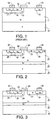
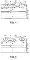
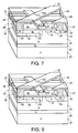
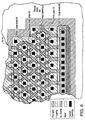
- Transistor DMOS agencé sous la forme d'une structure cellulaire, comprenant :caractérisé en ce que chacune desdites ouvertures est à peu près un polygone allongé en forme de losange, dont le grand axe situé entre deux sommets dudit polygone forme bissectrice de ladite ouverture, et le petit axe, est perpendiculaire au grand axe, entre deux autres sommets dudit polygone, ledit petit axe formant bissectrice de chacune desdites ouvertures et croisant ledit grand axe au niveau du point médian de ce dernier.un matériau semiconducteur (22) possédant un premier type de conductivité (N) et une première concentration de dopant, ledit matériau semiconducteur possédant une surface supérieure;une grille conductrice (26) recouvrant ladite surface supérieure dudit matériau semiconducteur en en étant isolée, ladite grille conductrice formant un treillis possédant une pluralité d'ouvertures sensiblement identiques (32,34);une pluralité de premières régions (31) formées dudit matériau semiconducteur, lesdites premières régions possédant ledit premier type de conductivité (N) et une seconde concentration de dopant pour former des régions de migration améliorées et sensiblement identiques dudit transistor DMOS, dans lequel ladite seconde concentration de dopant est supérieure à ladite première concentration de dopant;une pluralité de secondes régions (34) dudit matériau semiconducteur, lesdites secondes régions possédant ledit premier type de conductivité (N) et une troisième concentration de dopant supérieure à ladite seconde concentration de dopant pour former des régions de drain sensiblement identiques dudit transistor DMOS, dans lequel lesdites première et seconde régions sont en contact avec l'une respective desdites premières régions, chacune desdites secondes régions est séparée de ladite grille conductrice (26) par une première distance nécessaire pour l'obtention d'une première tension de claquage, et chacune desdites secondes régions est située au-dessous de l'une desdites ouvertures (34) dans ledit treillis;une pluralité de troisièmes régions (29) dudit matériau semiconducteur, lesdites troisièmes régions possédant un second type de conductivité (P) et une quatrième concentration de dopant pour former des régions de corps sensiblement identiques dudit transistor DMOS, chacune desdites troisièmes régions possédant une première extrémité, ladite première extrémité de chacune desdites troisièmes régions étant située au-dessous de ladite grille conductrice (26);une pluralité de quatrièmes régions (32) dudit matériau semiconducteur, chacune desdites quatrièmes régions possédant ledit premier type de conductivité (N) et ladite troisième concentration de dopant pour former des régions de source sensiblement identiques dudit transistor DMOS, chacune desdites quatrièmes régions étant située à l'intérieur de l'une respective desdites troisièmes régions, et chacune desdites quatrièmes régions étant située au-dessous de l'une desdites ouvertures (32) dans ledit treillis;une première bande conductrice (52) de matériau recouvrant et étant en contact électrique avec des parties centrales d'une première rangée desdites régions de source (32), ladite première bande conductrice étant connectée à une tension de source; etune seconde bande conductrice (54) de matériau recouvrant et étant en contact électrique avec des parties centrales de la seconde rangée de régions de drain (34) au voisinage de ladite première rangée desdites régions de source,
- Transistor DMOS selon la revendication 1, comprenant en outre :une cinquième région (28) formée dans chacune desdites troisièmes régions (29), ladite cinquième région ayant ledit second type de conductivité (P) et possédant une cinquième concentration de dopant supérieure à ladite quatrième concentration de dopant.
- Transistor DMOS selon la revendication 1, dans lequel lesdites secondes régions sont situées à l'intérieur desdites premières régions (31).
- Transistor DMOS selon la revendication 1, dans lequel ledit premier type de conductivité est un type N.
- Transistor DMOS selon la revendication 1, dans lequel ledit matériau semiconducteur est une couche épitaxiale.
- Transistor DMOS selon la revendication 1, dans lequel ledit matériau semiconducteur est une région dopée possédant ledit premier type de conductivité.
- Transistor DMOS selon la revendication 1, dans lequel ledit transistor est interconnecté à d'autres composants dans un circuit intégré.
- Transistor DMOS selon la revendication 1, dans lequel ledit transistor est agencé sous la forme d'un composant discret.
- Transistor DMOS selon la revendication 1, dans lequel un rapport dudit grand axe audit petit axe est égal ou supérieur à environ 1,2.
- Transistor DMOS selon la revendication 1, dans lequel un rapport dudit grand axe audit petit axe est égal ou supérieur à environ 1,5.
- Transistor DMOS selon la revendication 1, dans lequel chacune desdites ouvertures (32,34) est un parallélogramme possédant deux angles internes dans la gamme d'environ 45° à 85° et deux angles internes dans la gamme d'environ 135° à 95°.
Applications Claiming Priority (5)
| Application Number | Priority Date | Filing Date | Title |
|---|---|---|---|
| US313471 | 1994-09-27 | ||
| US08/313,471 US5447876A (en) | 1993-11-19 | 1994-09-27 | Method of making a diamond shaped gate mesh for cellular MOS transistor array |
| US384168 | 1995-02-06 | ||
| US08/384,168 US5517046A (en) | 1993-11-19 | 1995-02-06 | High voltage lateral DMOS device with enhanced drift region |
| PCT/US1995/011959 WO1996010267A1 (fr) | 1994-09-27 | 1995-09-25 | Dispositif dmos lateral a haute tension avec region de migration accrue |
Publications (3)
| Publication Number | Publication Date |
|---|---|
| EP0788659A1 EP0788659A1 (fr) | 1997-08-13 |
| EP0788659A4 EP0788659A4 (fr) | 1997-09-10 |
| EP0788659B1 true EP0788659B1 (fr) | 1999-12-01 |
Family
ID=26978899
Family Applications (1)
| Application Number | Title | Priority Date | Filing Date |
|---|---|---|---|
| EP95933172A Expired - Lifetime EP0788659B1 (fr) | 1994-09-27 | 1995-09-25 | Dispositif dmos lateral a haute tension avec region de migration accrue |
Country Status (6)
| Country | Link |
|---|---|
| US (1) | US5517046A (fr) |
| EP (1) | EP0788659B1 (fr) |
| JP (1) | JPH10506755A (fr) |
| AU (1) | AU3593395A (fr) |
| DE (1) | DE69513680T2 (fr) |
| WO (1) | WO1996010267A1 (fr) |
Cited By (1)
| Publication number | Priority date | Publication date | Assignee | Title |
|---|---|---|---|---|
| WO2003043074A2 (fr) * | 2001-11-16 | 2003-05-22 | Europäische Gesellschaft Für Leistungshalbleiter Mbh | Composant semi-conducteur et procede pour mettre en contact un tel composant semi-conducteur |
Families Citing this family (86)
| Publication number | Priority date | Publication date | Assignee | Title |
|---|---|---|---|---|
| US6242787B1 (en) | 1995-11-15 | 2001-06-05 | Denso Corporation | Semiconductor device and manufacturing method thereof |
| US6831331B2 (en) | 1995-11-15 | 2004-12-14 | Denso Corporation | Power MOS transistor for absorbing surge current |
| US6071768A (en) * | 1996-05-17 | 2000-06-06 | Texas Instruments Incorporated | Method of making an efficient NPN turn-on in a high voltage DENMOS transistor for ESD protection |
| SE513283C2 (sv) * | 1996-07-26 | 2000-08-14 | Ericsson Telefon Ab L M | MOS-transistorstruktur med utsträckt driftregion |
| US5846866A (en) * | 1997-02-07 | 1998-12-08 | National Semiconductor Corporation | Drain extension regions in low voltage lateral DMOS devices |
| WO1998053505A2 (fr) * | 1997-05-23 | 1998-11-26 | Koninklijke Philips Electronics N.V. | Dispositif de transistor mos lateral |
| EP0880183A3 (fr) * | 1997-05-23 | 1999-07-28 | Texas Instruments Incorporated | Dispositif de puissance LDMOS |
| KR100244282B1 (ko) * | 1997-08-25 | 2000-02-01 | 김영환 | 고전압 트랜지스터의 구조 및 제조 방법 |
| US6133077A (en) | 1998-01-13 | 2000-10-17 | Lsi Logic Corporation | Formation of high-voltage and low-voltage devices on a semiconductor substrate |
| US6020239A (en) * | 1998-01-28 | 2000-02-01 | International Business Machines Corporation | Pillar transistor incorporating a body contact |
| US6150200A (en) * | 1998-04-03 | 2000-11-21 | Motorola, Inc. | Semiconductor device and method of making |
| US6303961B1 (en) * | 1998-04-29 | 2001-10-16 | Aqere Systems Guardian Corp. | Complementary semiconductor devices |
| US6096606A (en) * | 1998-05-04 | 2000-08-01 | Motorola, Inc. | Method of making a semiconductor device |
| US6093585A (en) * | 1998-05-08 | 2000-07-25 | Lsi Logic Corporation | High voltage tolerant thin film transistor |
| US6252278B1 (en) * | 1998-05-18 | 2001-06-26 | Monolithic Power Systems, Inc. | Self-aligned lateral DMOS with spacer drift region |
| JP3443355B2 (ja) * | 1999-03-12 | 2003-09-02 | 三洋電機株式会社 | 半導体装置の製造方法 |
| KR100336557B1 (ko) * | 1999-09-14 | 2002-05-11 | 박종섭 | 정전방전보호소자 제조방법 |
| US6271552B1 (en) * | 1999-10-04 | 2001-08-07 | Xemod, Inc | Lateral RF MOS device with improved breakdown voltage |
| US6784059B1 (en) * | 1999-10-29 | 2004-08-31 | Sanyo Electric Co., Ltd. | Semiconductor device and method of manufacturing thereof |
| US6683349B1 (en) * | 1999-10-29 | 2004-01-27 | Sanyo Electric Co., Ltd. | Semiconductor device and method of manufacturing the same |
| ATE514192T1 (de) * | 2000-03-31 | 2011-07-15 | Ihp Gmbh | Cmos-kompatibler lateraler dmos-transistor |
| TW512533B (en) | 2000-04-26 | 2002-12-01 | Sanyo Electric Co | Semiconductor device and its manufacturing process |
| EP1158583A1 (fr) * | 2000-05-23 | 2001-11-28 | STMicroelectronics S.r.l. | LDMOS à faible résistance à l'état conducteur |
| JP2002094063A (ja) * | 2000-09-11 | 2002-03-29 | Toshiba Corp | 半導体装置 |
| JP2002217407A (ja) * | 2001-01-16 | 2002-08-02 | Sanyo Electric Co Ltd | 半導体装置とその製造方法 |
| JP4030269B2 (ja) * | 2001-03-06 | 2008-01-09 | 三洋電機株式会社 | 半導体装置とその製造方法 |
| US6683346B2 (en) * | 2001-03-09 | 2004-01-27 | Fairchild Semiconductor Corporation | Ultra dense trench-gated power-device with the reduced drain-source feedback capacitance and Miller charge |
| US7109558B2 (en) | 2001-06-06 | 2006-09-19 | Denso Corporation | Power MOS transistor having capability for setting substrate potential independently of source potential |
| US7033876B2 (en) * | 2001-07-03 | 2006-04-25 | Siliconix Incorporated | Trench MIS device having implanted drain-drift region and thick bottom oxide and process for manufacturing the same |
| US7291884B2 (en) * | 2001-07-03 | 2007-11-06 | Siliconix Incorporated | Trench MIS device having implanted drain-drift region and thick bottom oxide |
| US7009247B2 (en) * | 2001-07-03 | 2006-03-07 | Siliconix Incorporated | Trench MIS device with thick oxide layer in bottom of gate contact trench |
| US20060038223A1 (en) * | 2001-07-03 | 2006-02-23 | Siliconix Incorporated | Trench MOSFET having drain-drift region comprising stack of implanted regions |
| US6563142B2 (en) | 2001-07-11 | 2003-05-13 | Lumileds Lighting, U.S., Llc | Reducing the variation of far-field radiation patterns of flipchip light emitting diodes |
| US6486034B1 (en) * | 2001-07-20 | 2002-11-26 | Taiwan Semiconductor Manufacturing Company | Method of forming LDMOS device with double N-layering |
| US6475870B1 (en) * | 2001-07-23 | 2002-11-05 | Taiwan Semiconductor Manufacturing Company | P-type LDMOS device with buried layer to solve punch-through problems and process for its manufacture |
| US6593621B2 (en) | 2001-08-23 | 2003-07-15 | Micrel, Inc. | LDMOS field effect transistor with improved ruggedness in narrow curved areas |
| JP2003303961A (ja) * | 2002-04-09 | 2003-10-24 | Sanyo Electric Co Ltd | Mos半導体装置 |
| US7635621B2 (en) * | 2002-11-22 | 2009-12-22 | Micrel, Inc. | Lateral double-diffused metal oxide semiconductor (LDMOS) device with an enhanced drift region that has an improved Ron area product |
| US6833586B2 (en) * | 2003-01-02 | 2004-12-21 | Micrel, Inc. | LDMOS transistor with high voltage source and drain terminals |
| KR100493059B1 (ko) * | 2003-04-18 | 2005-06-02 | 삼성전자주식회사 | 게이트 캐패시턴스를 감소시킬 수 있는 트랜지스터 |
| US6946706B1 (en) | 2003-07-09 | 2005-09-20 | National Semiconductor Corporation | LDMOS transistor structure for improving hot carrier reliability |
| US20050275027A1 (en) * | 2003-09-09 | 2005-12-15 | Micrel, Incorporated | ESD protection for integrated circuits |
| DE10393627T5 (de) * | 2003-09-18 | 2005-10-13 | Shindengen Electric Mfg. Co. Ltd. | Lateraler Kurzkanal-dmos, Verfahren zur Herstellung desselben und Halbleiterbauelement |
| JP4800566B2 (ja) * | 2003-10-06 | 2011-10-26 | ルネサスエレクトロニクス株式会社 | 半導体装置及びその製造方法 |
| CN100376020C (zh) * | 2003-12-29 | 2008-03-19 | 中芯国际集成电路制造(上海)有限公司 | 一种制作具有延伸闸极晶体管的方法 |
| US20050280053A1 (en) * | 2004-06-22 | 2005-12-22 | Hayes Monty B | Semiconductor device with diagonal gate signal distribution runner |
| US7718448B1 (en) * | 2005-05-27 | 2010-05-18 | National Semiconductor Corporation | Method of monitoring process misalignment to reduce asymmetric device operation and improve the electrical and hot carrier performance of LDMOS transistor arrays |
| US7868378B1 (en) * | 2005-07-18 | 2011-01-11 | Volterra Semiconductor Corporation | Methods and apparatus for LDMOS transistors |
| US7375408B2 (en) * | 2005-10-11 | 2008-05-20 | United Microelectronics Corp. | Fabricating method of a high voltage metal oxide semiconductor device |
| US7956384B2 (en) * | 2006-06-23 | 2011-06-07 | Alpha & Omega Semiconductor Ltd. | Closed cell configuration to increase channel density for sub-micron planar semiconductor power device |
| TWI312192B (en) * | 2006-09-18 | 2009-07-11 | Promos Technologies Inc | Semiconductor device and manufacture method thereof |
| US7737526B2 (en) * | 2007-03-28 | 2010-06-15 | Advanced Analogic Technologies, Inc. | Isolated trench MOSFET in epi-less semiconductor sustrate |
| CN100592533C (zh) * | 2007-10-15 | 2010-02-24 | 天钰科技股份有限公司 | 横向扩散金属氧化物晶体管 |
| TWI394277B (zh) * | 2007-10-19 | 2013-04-21 | Fitipower Integrated Tech Inc | 橫向擴散金屬氧化物電晶體 |
| US7999318B2 (en) * | 2007-12-28 | 2011-08-16 | Volterra Semiconductor Corporation | Heavily doped region in double-diffused source MOSFET (LDMOS) transistor and a method of fabricating the same |
| EP2232560A4 (fr) | 2008-01-14 | 2012-05-02 | Volterra Semiconductor Corp | Transistor de puissance ayant un canal protégé |
| JP2009239096A (ja) * | 2008-03-27 | 2009-10-15 | Renesas Technology Corp | 半導体装置 |
| US8114750B2 (en) * | 2008-04-17 | 2012-02-14 | International Business Machines Corporation | Lateral diffusion field effect transistor with drain region self-aligned to gate electrode |
| JP5420854B2 (ja) * | 2008-04-28 | 2014-02-19 | パナソニック株式会社 | 半導体装置およびその製造方法 |
| US7851314B2 (en) * | 2008-04-30 | 2010-12-14 | Alpha And Omega Semiconductor Incorporated | Short channel lateral MOSFET and method |
| US7759923B2 (en) * | 2008-07-08 | 2010-07-20 | Micrel, Inc. | Current sensing in a buck-boost switching regulator using integrally embedded PMOS devices |
| KR20100064264A (ko) * | 2008-12-04 | 2010-06-14 | 주식회사 동부하이텍 | 반도체 소자 및 이의 제조 방법 |
| US8049307B2 (en) * | 2009-01-23 | 2011-11-01 | Vanguard International Semiconductor Corporation | Insulated gate bipolar transistor (IGBT) electrostatic discharge (ESD) protection devices |
| JP5525736B2 (ja) * | 2009-02-18 | 2014-06-18 | セミコンダクター・コンポーネンツ・インダストリーズ・リミテッド・ライアビリティ・カンパニー | 半導体装置及びその製造方法 |
| US9184097B2 (en) * | 2009-03-12 | 2015-11-10 | System General Corporation | Semiconductor devices and formation methods thereof |
| US9064947B2 (en) * | 2009-08-04 | 2015-06-23 | Gan Systems Inc. | Island matrixed gallium nitride microwave and power switching transistors |
| US8048765B2 (en) * | 2009-08-28 | 2011-11-01 | Broadcom Corporation | Method for fabricating a MOS transistor with source/well heterojunction and related structure |
| US20110062554A1 (en) * | 2009-09-17 | 2011-03-17 | Hsing Michael R | High voltage floating well in a silicon die |
| DE102009051745B4 (de) | 2009-11-03 | 2017-09-21 | Austriamicrosystems Ag | Hochvolt-Transistor mit Mehrfach-Dielektrikum und Herstellungsverfahren |
| JP5784269B2 (ja) * | 2009-11-11 | 2015-09-24 | ルネサスエレクトロニクス株式会社 | 半導体装置及びその製造方法 |
| KR101128694B1 (ko) * | 2009-11-17 | 2012-03-23 | 매그나칩 반도체 유한회사 | 반도체 장치 |
| US8362557B2 (en) | 2009-12-02 | 2013-01-29 | Fairchild Semiconductor Corporation | Stepped-source LDMOS architecture |
| US8390078B2 (en) * | 2010-06-10 | 2013-03-05 | Taiwan Semiconductor Manufacturing Company, Ltd. | Quadrangle MOS transistors |
| JP5043990B2 (ja) * | 2010-06-18 | 2012-10-10 | シャープ株式会社 | 半導体装置およびその製造方法 |
| US9450074B1 (en) * | 2011-07-29 | 2016-09-20 | Maxim Integrated Products, Inc. | LDMOS with field plate connected to gate |
| US9214457B2 (en) | 2011-09-20 | 2015-12-15 | Alpha & Omega Semiconductor Incorporated | Method of integrating high voltage devices |
| US8916913B2 (en) * | 2012-07-13 | 2014-12-23 | Monolithic Power Systems, Inc. | High voltage semiconductor device and the associated method of manufacturing |
| US20140175526A1 (en) * | 2012-12-20 | 2014-06-26 | Macronix International Co., Ltd. | Semiconductor device for current control and method thereof |
| US8981475B2 (en) | 2013-06-18 | 2015-03-17 | International Business Machines Corporation | Lateral diffusion metal oxide semiconductor (LDMOS) |
| US10861938B2 (en) * | 2013-07-19 | 2020-12-08 | Nissan Motor Co., Ltd. | Semiconductor device and method of manufacturing the same |
| US9219146B2 (en) * | 2013-12-27 | 2015-12-22 | Monolithic Power Systems, Inc. | High voltage PMOS and the method for forming thereof |
| GB201418752D0 (en) * | 2014-10-22 | 2014-12-03 | Rolls Royce Plc | Lateral field effect transistor device |
| US9583612B1 (en) * | 2016-01-21 | 2017-02-28 | Texas Instruments Incorporated | Drift region implant self-aligned to field relief oxide with sidewall dielectric |
| US20170292047A1 (en) | 2016-04-12 | 2017-10-12 | Rextac Llc | Hexene-1 Containing Amorphous Polyalphaolefins For Improved Hot Melt Adhesives |
| TWM547757U (zh) | 2017-01-20 | 2017-08-21 | 杰力科技股份有限公司 | 功率晶片及其電晶體結構 |
| KR20190118745A (ko) * | 2018-04-11 | 2019-10-21 | 주식회사 디비하이텍 | 3d 채널 영역을 형성하는 반도체 소자 및 제조방법 |
Family Cites Families (9)
| Publication number | Priority date | Publication date | Assignee | Title |
|---|---|---|---|---|
| US4148047A (en) * | 1978-01-16 | 1979-04-03 | Honeywell Inc. | Semiconductor apparatus |
| JPS63262873A (ja) * | 1987-04-21 | 1988-10-31 | Fuji Xerox Co Ltd | 半導体装置 |
| US4922327A (en) * | 1987-12-24 | 1990-05-01 | University Of Toronto Innovations Foundation | Semiconductor LDMOS device with upper and lower passages |
| JPH01207976A (ja) * | 1988-02-15 | 1989-08-21 | Nec Corp | 半導体装置 |
| US5072267A (en) * | 1989-06-28 | 1991-12-10 | Nec Corporation | Complementary field effect transistor |
| JP2545762B2 (ja) * | 1990-04-13 | 1996-10-23 | 日本電装株式会社 | 高耐圧misトランジスタおよびこのトランジスタを有する相補型トランジスタの製造方法 |
| US5306652A (en) * | 1991-12-30 | 1994-04-26 | Texas Instruments Incorporated | Lateral double diffused insulated gate field effect transistor fabrication process |
| US5412239A (en) * | 1993-05-14 | 1995-05-02 | Siliconix Incorporated | Contact geometry for improved lateral MOSFET |
| US5355008A (en) * | 1993-11-19 | 1994-10-11 | Micrel, Inc. | Diamond shaped gate mesh for cellular MOS transistor array |
-
1995
- 1995-02-06 US US08/384,168 patent/US5517046A/en not_active Expired - Lifetime
- 1995-09-25 AU AU35933/95A patent/AU3593395A/en not_active Abandoned
- 1995-09-25 WO PCT/US1995/011959 patent/WO1996010267A1/fr active IP Right Grant
- 1995-09-25 EP EP95933172A patent/EP0788659B1/fr not_active Expired - Lifetime
- 1995-09-25 JP JP8511865A patent/JPH10506755A/ja active Pending
- 1995-09-25 DE DE69513680T patent/DE69513680T2/de not_active Expired - Fee Related
Cited By (5)
| Publication number | Priority date | Publication date | Assignee | Title |
|---|---|---|---|---|
| WO2003043074A2 (fr) * | 2001-11-16 | 2003-05-22 | Europäische Gesellschaft Für Leistungshalbleiter Mbh | Composant semi-conducteur et procede pour mettre en contact un tel composant semi-conducteur |
| WO2003043074A3 (fr) * | 2001-11-16 | 2004-04-15 | Europaeische Ges Fuer Leistung | Composant semi-conducteur et procede pour mettre en contact un tel composant semi-conducteur |
| US7151318B2 (en) | 2001-11-16 | 2006-12-19 | Eupec Europaische Gesellschaft Fur Leistungshalbleiter Gmbh & Co. Kg | Semiconductor component and method for contacting said semiconductor component |
| US7462557B2 (en) | 2001-11-16 | 2008-12-09 | Infineon Technologies Ag | Semiconductor component and method for contracting said semiconductor component |
| USRE47854E1 (en) | 2001-11-16 | 2020-02-11 | Infineon Technologies Ag | Semiconductor component and method for contacting said semiconductor component |
Also Published As
| Publication number | Publication date |
|---|---|
| AU3593395A (en) | 1996-04-19 |
| WO1996010267A1 (fr) | 1996-04-04 |
| DE69513680D1 (de) | 2000-01-05 |
| EP0788659A1 (fr) | 1997-08-13 |
| DE69513680T2 (de) | 2000-05-11 |
| US5517046A (en) | 1996-05-14 |
| EP0788659A4 (fr) | 1997-09-10 |
| JPH10506755A (ja) | 1998-06-30 |
Similar Documents
| Publication | Publication Date | Title |
|---|---|---|
| EP0788659B1 (fr) | Dispositif dmos lateral a haute tension avec region de migration accrue | |
| US5447876A (en) | Method of making a diamond shaped gate mesh for cellular MOS transistor array | |
| US7663186B2 (en) | Semiconductor device | |
| US7635621B2 (en) | Lateral double-diffused metal oxide semiconductor (LDMOS) device with an enhanced drift region that has an improved Ron area product | |
| US6518138B2 (en) | Method of forming Self-aligned lateral DMOS with spacer drift region | |
| EP1292990B1 (fr) | Transistor mos a tranchees avec profil de corps a double diffusion | |
| US5382536A (en) | Method of fabricating lateral DMOS structure | |
| US20010012663A1 (en) | Single feature size mos technology power device | |
| EP0747966A2 (fr) | DMOS quasi-vertical par un procédé BICMOS ou MOS de grande efficacité | |
| US7446354B2 (en) | Power semiconductor device having improved performance and method | |
| US6972231B2 (en) | Rad Hard MOSFET with graded body diode junction and reduced on resistance | |
| US5486718A (en) | High voltage planar edge termination structure and method of making same | |
| US7732862B2 (en) | Power semiconductor device having improved performance and method | |
| US6548864B2 (en) | High density MOS technology power device | |
| US5703389A (en) | Vertical IGFET configuration having low on-resistance and method | |
| JP4990140B2 (ja) | パワー半導体デバイス | |
| GB2045525A (en) | Field effect transistor construction | |
| US5321291A (en) | Power MOSFET transistor | |
| US6486512B2 (en) | Power semiconductor device having high breakdown voltage and method for fabricating the same | |
| US7432145B2 (en) | Power semiconductor device with a base region and method of manufacturing same | |
| JP2926962B2 (ja) | Mis型電界効果トランジスタを有する半導体装置 | |
| US20050116298A1 (en) | MOS field effect transistor with small miller capacitance | |
| JPH0644605B2 (ja) | 高耐圧mos電界効界半導体装置の製造方法 |
Legal Events
| Date | Code | Title | Description |
|---|---|---|---|
| PUAI | Public reference made under article 153(3) epc to a published international application that has entered the european phase |
Free format text: ORIGINAL CODE: 0009012 |
|
| 17P | Request for examination filed |
Effective date: 19970424 |
|
| AK | Designated contracting states |
Kind code of ref document: A1 Designated state(s): DE FR GB IT NL |
|
| A4 | Supplementary search report drawn up and despatched |
Effective date: 19970729 |
|
| AK | Designated contracting states |
Kind code of ref document: A4 Designated state(s): DE FR GB IT NL |
|
| 17Q | First examination report despatched |
Effective date: 19980414 |
|
| GRAG | Despatch of communication of intention to grant |
Free format text: ORIGINAL CODE: EPIDOS AGRA |
|
| GRAG | Despatch of communication of intention to grant |
Free format text: ORIGINAL CODE: EPIDOS AGRA |
|
| GRAH | Despatch of communication of intention to grant a patent |
Free format text: ORIGINAL CODE: EPIDOS IGRA |
|
| GRAH | Despatch of communication of intention to grant a patent |
Free format text: ORIGINAL CODE: EPIDOS IGRA |
|
| GRAA | (expected) grant |
Free format text: ORIGINAL CODE: 0009210 |
|
| AK | Designated contracting states |
Kind code of ref document: B1 Designated state(s): DE FR GB IT NL |
|
| REF | Corresponds to: |
Ref document number: 69513680 Country of ref document: DE Date of ref document: 20000105 |
|
| ET | Fr: translation filed | ||
| ITF | It: translation for a ep patent filed |
Owner name: STUDIO TORTA S.R.L. |
|
| PGFP | Annual fee paid to national office [announced via postgrant information from national office to epo] |
Ref country code: DE Payment date: 20000905 Year of fee payment: 6 |
|
| PLBE | No opposition filed within time limit |
Free format text: ORIGINAL CODE: 0009261 |
|
| STAA | Information on the status of an ep patent application or granted ep patent |
Free format text: STATUS: NO OPPOSITION FILED WITHIN TIME LIMIT |
|
| 26N | No opposition filed | ||
| PGFP | Annual fee paid to national office [announced via postgrant information from national office to epo] |
Ref country code: NL Payment date: 20010831 Year of fee payment: 7 Ref country code: FR Payment date: 20010831 Year of fee payment: 7 |
|
| REG | Reference to a national code |
Ref country code: GB Ref legal event code: IF02 |
|
| PG25 | Lapsed in a contracting state [announced via postgrant information from national office to epo] |
Ref country code: DE Free format text: LAPSE BECAUSE OF NON-PAYMENT OF DUE FEES Effective date: 20020501 |
|
| PG25 | Lapsed in a contracting state [announced via postgrant information from national office to epo] |
Ref country code: NL Free format text: LAPSE BECAUSE OF NON-PAYMENT OF DUE FEES Effective date: 20030401 |
|
| PG25 | Lapsed in a contracting state [announced via postgrant information from national office to epo] |
Ref country code: FR Free format text: LAPSE BECAUSE OF NON-PAYMENT OF DUE FEES Effective date: 20030603 |
|
| REG | Reference to a national code |
Ref country code: FR Ref legal event code: ST |
|
| PG25 | Lapsed in a contracting state [announced via postgrant information from national office to epo] |
Ref country code: IT Free format text: LAPSE BECAUSE OF NON-PAYMENT OF DUE FEES Effective date: 20050925 |
|
| PGFP | Annual fee paid to national office [announced via postgrant information from national office to epo] |
Ref country code: GB Payment date: 20140929 Year of fee payment: 20 |
|
| REG | Reference to a national code |
Ref country code: GB Ref legal event code: PE20 Expiry date: 20150924 |
|
| PG25 | Lapsed in a contracting state [announced via postgrant information from national office to epo] |
Ref country code: GB Free format text: LAPSE BECAUSE OF EXPIRATION OF PROTECTION Effective date: 20150924 |