EP0755044B1 - Verfahren und Einrichtung zur Steuerung einer Flüssigkristallanzeige mit Vorladen von Anzeigedatenleitungen - Google Patents
Verfahren und Einrichtung zur Steuerung einer Flüssigkristallanzeige mit Vorladen von Anzeigedatenleitungen Download PDFInfo
- Publication number
- EP0755044B1 EP0755044B1 EP96304946A EP96304946A EP0755044B1 EP 0755044 B1 EP0755044 B1 EP 0755044B1 EP 96304946 A EP96304946 A EP 96304946A EP 96304946 A EP96304946 A EP 96304946A EP 0755044 B1 EP0755044 B1 EP 0755044B1
- Authority
- EP
- European Patent Office
- Prior art keywords
- data
- voltage
- data line
- driving
- lines
- Prior art date
- Legal status (The legal status is an assumption and is not a legal conclusion. Google has not performed a legal analysis and makes no representation as to the accuracy of the status listed.)
- Expired - Lifetime
Links
- 239000004973 liquid crystal related substance Substances 0.000 title claims description 59
- 238000000034 method Methods 0.000 title claims description 22
- 239000003990 capacitor Substances 0.000 claims description 6
- 239000000758 substrate Substances 0.000 description 15
- 238000002834 transmittance Methods 0.000 description 15
- 239000004020 conductor Substances 0.000 description 6
- 238000013459 approach Methods 0.000 description 4
- 230000005540 biological transmission Effects 0.000 description 4
- 238000010586 diagram Methods 0.000 description 4
- 239000011159 matrix material Substances 0.000 description 4
- 238000004088 simulation Methods 0.000 description 3
- XUIMIQQOPSSXEZ-UHFFFAOYSA-N Silicon Chemical compound [Si] XUIMIQQOPSSXEZ-UHFFFAOYSA-N 0.000 description 2
- 229910021417 amorphous silicon Inorganic materials 0.000 description 2
- 239000013078 crystal Substances 0.000 description 2
- 238000002474 experimental method Methods 0.000 description 2
- 238000004519 manufacturing process Methods 0.000 description 2
- 229910021420 polycrystalline silicon Inorganic materials 0.000 description 2
- 229920005591 polysilicon Polymers 0.000 description 2
- 229910052710 silicon Inorganic materials 0.000 description 2
- 239000010703 silicon Substances 0.000 description 2
- 239000010409 thin film Substances 0.000 description 2
- 230000015572 biosynthetic process Effects 0.000 description 1
- 238000011161 development Methods 0.000 description 1
- 230000010365 information processing Effects 0.000 description 1
- 238000007689 inspection Methods 0.000 description 1
- 239000000463 material Substances 0.000 description 1
- 229920001296 polysiloxane Polymers 0.000 description 1
- 125000006850 spacer group Chemical group 0.000 description 1
Images


Classifications
-
- G—PHYSICS
- G02—OPTICS
- G02F—OPTICAL DEVICES OR ARRANGEMENTS FOR THE CONTROL OF LIGHT BY MODIFICATION OF THE OPTICAL PROPERTIES OF THE MEDIA OF THE ELEMENTS INVOLVED THEREIN; NON-LINEAR OPTICS; FREQUENCY-CHANGING OF LIGHT; OPTICAL LOGIC ELEMENTS; OPTICAL ANALOGUE/DIGITAL CONVERTERS
- G02F1/00—Devices or arrangements for the control of the intensity, colour, phase, polarisation or direction of light arriving from an independent light source, e.g. switching, gating or modulating; Non-linear optics
- G02F1/01—Devices or arrangements for the control of the intensity, colour, phase, polarisation or direction of light arriving from an independent light source, e.g. switching, gating or modulating; Non-linear optics for the control of the intensity, phase, polarisation or colour
- G02F1/13—Devices or arrangements for the control of the intensity, colour, phase, polarisation or direction of light arriving from an independent light source, e.g. switching, gating or modulating; Non-linear optics for the control of the intensity, phase, polarisation or colour based on liquid crystals, e.g. single liquid crystal display cells
- G02F1/133—Constructional arrangements; Operation of liquid crystal cells; Circuit arrangements
-
- G—PHYSICS
- G09—EDUCATION; CRYPTOGRAPHY; DISPLAY; ADVERTISING; SEALS
- G09G—ARRANGEMENTS OR CIRCUITS FOR CONTROL OF INDICATING DEVICES USING STATIC MEANS TO PRESENT VARIABLE INFORMATION
- G09G3/00—Control arrangements or circuits, of interest only in connection with visual indicators other than cathode-ray tubes
- G09G3/20—Control arrangements or circuits, of interest only in connection with visual indicators other than cathode-ray tubes for presentation of an assembly of a number of characters, e.g. a page, by composing the assembly by combination of individual elements arranged in a matrix no fixed position being assigned to or needed to be assigned to the individual characters or partial characters
- G09G3/34—Control arrangements or circuits, of interest only in connection with visual indicators other than cathode-ray tubes for presentation of an assembly of a number of characters, e.g. a page, by composing the assembly by combination of individual elements arranged in a matrix no fixed position being assigned to or needed to be assigned to the individual characters or partial characters by control of light from an independent source
- G09G3/36—Control arrangements or circuits, of interest only in connection with visual indicators other than cathode-ray tubes for presentation of an assembly of a number of characters, e.g. a page, by composing the assembly by combination of individual elements arranged in a matrix no fixed position being assigned to or needed to be assigned to the individual characters or partial characters by control of light from an independent source using liquid crystals
- G09G3/3611—Control of matrices with row and column drivers
- G09G3/3685—Details of drivers for data electrodes
- G09G3/3688—Details of drivers for data electrodes suitable for active matrices only
-
- G—PHYSICS
- G09—EDUCATION; CRYPTOGRAPHY; DISPLAY; ADVERTISING; SEALS
- G09G—ARRANGEMENTS OR CIRCUITS FOR CONTROL OF INDICATING DEVICES USING STATIC MEANS TO PRESENT VARIABLE INFORMATION
- G09G2310/00—Command of the display device
- G09G2310/02—Addressing, scanning or driving the display screen or processing steps related thereto
- G09G2310/0243—Details of the generation of driving signals
- G09G2310/0248—Precharge or discharge of column electrodes before or after applying exact column voltages
-
- G—PHYSICS
- G09—EDUCATION; CRYPTOGRAPHY; DISPLAY; ADVERTISING; SEALS
- G09G—ARRANGEMENTS OR CIRCUITS FOR CONTROL OF INDICATING DEVICES USING STATIC MEANS TO PRESENT VARIABLE INFORMATION
- G09G2310/00—Command of the display device
- G09G2310/02—Addressing, scanning or driving the display screen or processing steps related thereto
- G09G2310/0243—Details of the generation of driving signals
- G09G2310/0251—Precharge or discharge of pixel before applying new pixel voltage
-
- G—PHYSICS
- G09—EDUCATION; CRYPTOGRAPHY; DISPLAY; ADVERTISING; SEALS
- G09G—ARRANGEMENTS OR CIRCUITS FOR CONTROL OF INDICATING DEVICES USING STATIC MEANS TO PRESENT VARIABLE INFORMATION
- G09G2310/00—Command of the display device
- G09G2310/02—Addressing, scanning or driving the display screen or processing steps related thereto
- G09G2310/0264—Details of driving circuits
- G09G2310/0297—Special arrangements with multiplexing or demultiplexing of display data in the drivers for data electrodes, in a pre-processing circuitry delivering display data to said drivers or in the matrix panel, e.g. multiplexing plural data signals to one D/A converter or demultiplexing the D/A converter output to multiple columns
-
- G—PHYSICS
- G09—EDUCATION; CRYPTOGRAPHY; DISPLAY; ADVERTISING; SEALS
- G09G—ARRANGEMENTS OR CIRCUITS FOR CONTROL OF INDICATING DEVICES USING STATIC MEANS TO PRESENT VARIABLE INFORMATION
- G09G2330/00—Aspects of power supply; Aspects of display protection and defect management
- G09G2330/02—Details of power systems and of start or stop of display operation
- G09G2330/021—Power management, e.g. power saving
- G09G2330/023—Power management, e.g. power saving using energy recovery or conservation
-
- G—PHYSICS
- G09—EDUCATION; CRYPTOGRAPHY; DISPLAY; ADVERTISING; SEALS
- G09G—ARRANGEMENTS OR CIRCUITS FOR CONTROL OF INDICATING DEVICES USING STATIC MEANS TO PRESENT VARIABLE INFORMATION
- G09G2330/00—Aspects of power supply; Aspects of display protection and defect management
- G09G2330/12—Test circuits or failure detection circuits included in a display system, as permanent part thereof
-
- G—PHYSICS
- G09—EDUCATION; CRYPTOGRAPHY; DISPLAY; ADVERTISING; SEALS
- G09G—ARRANGEMENTS OR CIRCUITS FOR CONTROL OF INDICATING DEVICES USING STATIC MEANS TO PRESENT VARIABLE INFORMATION
- G09G3/00—Control arrangements or circuits, of interest only in connection with visual indicators other than cathode-ray tubes
- G09G3/20—Control arrangements or circuits, of interest only in connection with visual indicators other than cathode-ray tubes for presentation of an assembly of a number of characters, e.g. a page, by composing the assembly by combination of individual elements arranged in a matrix no fixed position being assigned to or needed to be assigned to the individual characters or partial characters
- G09G3/2007—Display of intermediate tones
- G09G3/2011—Display of intermediate tones by amplitude modulation
-
- G—PHYSICS
- G09—EDUCATION; CRYPTOGRAPHY; DISPLAY; ADVERTISING; SEALS
- G09G—ARRANGEMENTS OR CIRCUITS FOR CONTROL OF INDICATING DEVICES USING STATIC MEANS TO PRESENT VARIABLE INFORMATION
- G09G3/00—Control arrangements or circuits, of interest only in connection with visual indicators other than cathode-ray tubes
- G09G3/20—Control arrangements or circuits, of interest only in connection with visual indicators other than cathode-ray tubes for presentation of an assembly of a number of characters, e.g. a page, by composing the assembly by combination of individual elements arranged in a matrix no fixed position being assigned to or needed to be assigned to the individual characters or partial characters
- G09G3/34—Control arrangements or circuits, of interest only in connection with visual indicators other than cathode-ray tubes for presentation of an assembly of a number of characters, e.g. a page, by composing the assembly by combination of individual elements arranged in a matrix no fixed position being assigned to or needed to be assigned to the individual characters or partial characters by control of light from an independent source
- G09G3/36—Control arrangements or circuits, of interest only in connection with visual indicators other than cathode-ray tubes for presentation of an assembly of a number of characters, e.g. a page, by composing the assembly by combination of individual elements arranged in a matrix no fixed position being assigned to or needed to be assigned to the individual characters or partial characters by control of light from an independent source using liquid crystals
- G09G3/3611—Control of matrices with row and column drivers
- G09G3/3614—Control of polarity reversal in general
Definitions
- the present invention relates to a device and method for driving a liquid crystal display, and, more particularly, to a method for driving a liquid crystal display having display cells each of which consists of a switching element connected to a data line and a gate line, a pair of electrodes oppositely disposed with a predetermined spacing, a liquid crystal disposed between the pair of electrodes and a driver for a liquid crystal display to which the driving method can be applied.
- a liquid crystal display is conventionally known as a display for displaying characters or images such as graphics on an information processing device such as a personal computer.
- An active matrix driven LCD which is composed by arranging switching elements such as thin film transistors (TFT) in a matrix is particularly promising as a display replacing a CRT because it can control intensity of pixels and is also suitable for display of dynamic images with fast movement and for color images.
- TFT LCD thin film transistors
- a number of display cells are arranged in a matrix.
- Each display cell comprises a pair of TFT and an electrode provided on a pair of opposed substrates, a transparent common electrode formed over the entire surface of another substrate (transparent substrate) and liquid crystal sealed between the pair of substrates.
- the former substrate is provided with a number of gate lines for turning on the TFTs by row, and a number of data lines for applying voltage on the liquid crystal through the TFTs which are turned on.
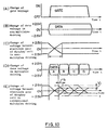
- a driving device for TFT LCD applies a voltage to the gate lines for a predetermined duration as shown in Figure 10 (A) to sequentially turn on the TFT of each display cell, and applies on each data line a voltage with intensity corresponding to a gradation value to be displayed on a display cell for which the TFT is turned on (data voltage) (see Figure 10 (B)).
- data voltage data voltage
- the liquid crystal of each display cell varies its light transmittance according to intensity of the voltage, and accumulates charges between the pair of electrodes. After the TFT is turned off, the accumulated charges maintain the state where the light transmittance is varied (see Figure 10 (C)). This causes an image to be displayed on the LCD.
- the life of liquid crystal is shortened if voltage with the same polarity continues to be applied.
- it is intended to extend the life of liquid crystal in such a manner that the liquid crystal is driven by reversing the polarity of data voltage, for example, every one line or one frame to reverse the data voltage applied to each display cell every time through utilization of the fact that the light transmittance of liquid crystals becomes equal even if the polarity differs as long as the absolute value of applied voltage is same.
- a driver for driving the data line of LCD
- a very large number of data lines for example, 1,000 lines
- driving circuits for example, four driver ICs having 250 output terminals (250 driving circuits) are necessary to be provided to drive 1,000 data lines.
- the pitch of LCD display cells is reduced to attain high definition of the LCD, this causes to reduce the pitch of data lines as well. For example, if it is reduced to about 15 microns, it physically becomes very difficult to mount the driver ICs.
- multiplex driving As a technique to overcome the above problems, it has been proposed to perform so-called multiplex driving wherein a driver having driving circuits of 1/n (n being an integer) in the number of data lines is provided, and a multiplexer is provided for selectively connecting the driver to any one of n sets of data line groups so that the driver and multiplexer sequentially drives n sets of data line groups.
- a driver having driving circuits of 1/n (n being an integer) in the number of data lines is provided, and a multiplexer is provided for selectively connecting the driver to any one of n sets of data line groups so that the driver and multiplexer sequentially drives n sets of data line groups.
- PCT patent application WO 94/10676 discloses a multiplexed driven display in which the data lines are all precharged to a value of approximately the maximum data voltage that can be displayed. Then, each of the data line groups have the data voltage applied sequentially.
- the present invention is made in view of the above facts, and is intended to obtain a device and method for driving a liquid crystal display which can display an image at high quality even if the duration to apply the data voltage is short.
- a device for driving a liquid crystal display is a driving device for driving a liquid crystal display in which a number of data lines and a number of gate lines are arranged to intersect with each other, and respective display cells are positioned at the intersections of the data and gate lines, the data lines consisting of a plurality of data line groups, each display cell consisting of a switching element connected to a data line and a gate line, a pair of electrodes oppositely positioned with a predetermined spacing, and liquid crystal disposed between the pair of electrodes, the driving device comprising gate line driving means connected to a number of the gate lines, and for applying a voltage to the gate lines to turn on for a predetermined duration the switching element of the display cell connected to the gate line, data line driving means connected to a number of the data lines, and for applying a data voltage to the data lines for the predetermined duration to change the voltage between the electrode pair of the display cell connected to the gate line to which the voltage is applied by the gate line driving means to a pre
- the data voltage is applied to the data line by the data line driving means in a state where the voltage is applied to the gate line and the switching element of respective display cells connected to the gate line is turned on.
- a current flows through the data line so that the voltage between the electrode pair of the display cell to which the data line is connected and the switching element of which is turned on is changed to a predetermined voltage.
- the time from starting of application of data voltage to change of voltage between the electrode pair to the predetermined voltage is affected by capacitance between the electrode pair and capacitance contained in the data line. In this case, generally, the capacitance of the data line has higher electrostatic capacity than that between the electrode pair, and is more influential.
- the present invention controls potential on a number of data lines with the potential control means so that the potential on the data line closes to the data voltage being applied before the data voltage is applied to the data line. Then, when the data voltage is applied to each data line, at least each data line would have potential at a value close to the data voltage being applied next.
- the time is shortened from starting of application of the data voltage to the time when the voltage between the electrode pair of the display cell reaches the predetermined voltage.
- the voltage between the electrode pair reaches the predetermined voltage corresponding to the magnitude of applied data voltage so that the light transmittance of the liquid crystal of each display cell can be caused to match that corresponding to the value of gradation to be displayed on each display cell.
- an image can be displayed with high quality even if the duration of application of data voltage is short.
- the present invention is the above driving device, wherein a number of the data lines consists of a plurality of data line groups, and the data line driving means sequentially applies a data voltage to the data line in each data line group in the predetermined duration.
- the above arrangement could perform multiplex driving in which the data voltage is sequentially applied to a number of data lines in each of data line groups.
- an image can be displayed at high quality even if the duration of data voltage application is short, the image can be displayed at high quality even when the multiplex ratio is increased, that is, even when the number of data lines constituting each data line group is reduced, and the number of data line groups is increased (this shortens the duration of data voltage application).
- the number of data lines constituting each data line group can be reduced, it is easily attained to increase the size and definition of a liquid crystal display.
- the potential control means controls the potential on the data line so that the voltage between the electrode pair becomes a value sufficient to change to the predetermined voltage while the data line driving means applies the data voltage to the data line.
- the potential control means may control the potential on the data line so that, for example, the potential on the data line becomes the average value of the data voltage applied by the data line driving means or the minimum absolute value of the data voltage.
- the present invention is the above driving device, wherein the data line driving means applies to parts of data lines a voltage with a polarity different from that to the remaining data lines, and the potential control means controls the potential on the data lines by electrically connecting the data lines applied with voltages with different polarities as the data voltage.
- the potential control means may control each of a number of data lines during the time from when the data line driving means applies the data voltage to the data line previous time to when it applies the data voltage next time.
- the present invention is the above driving device, wherein the potential control means controls the potential on the data line during the time when a voltage is being applied to the gate line connected to a display cell in which the voltage between the electrode pair is changed by the data voltage applied to the data line next time.
- the control of potential on the data line according to the present invention may be performed while a voltage is not being applied to any gate line.
- the voltage between the electrode pair of the display cell connected to the gate line also approaches to the data voltage applied next time as the potential on the data line is controlled so that it is possible to further shorten the time from starting of application of the data voltage to when the voltage between the electrode pair changes to a value corresponding to that of gradation to be displayed on the display cell.
- the duration of data voltage application can be further shortened.
- the potential control means may comprise potential changing means for changing the potential on the data line, a number of switching means provided between the potential changing means and a number of the data lines, and ON/OFF control means for controlling turning on/off of a number of the switching means.
- a method for driving a liquid crystal display is a driving method for driving a liquid crystal display in which a number of data lines and a number of gate lines are arranged to intersect with each other, and respective display cells are positioned at the intersections of the data and gate lines, the display cell consisting of a switching element connected to a data line and a gate line, a pair of electrodes oppositely positioned with a predetermined spacing, and liquid crystal disposed between the pair of electrodes, the driving method comprising steps of applying a voltage to the gate lines to turn on for a predetermined duration the switching element of the display cell connected to the gate line, applying a data voltage to the data line within the predetermined duration to change a voltage between the electrode pair of the display cell to a predetermined voltage, and controlling the potential on the data line so as to close to the data voltage being applied prior to the data voltage application step, whereby the control step allows to shorten the time from when the data voltage is applied to when the voltage between the electrode pair of the display cell reaches the predetermined voltage
- the present invention is the above driving method, wherein a number of the data lines consists of a plurality of data line groups, and the data voltage application step sequentially applies the data voltage by the data line group within the predetermined duration for each data line group.
- an image can be displayed at high quality even if the duration of data voltage application is short, the image can be displayed at high quality even when the multiplex ratio is increased, that is, even when the number of data lines constituting each data line group is reduced, and the number of data line groups is increased (this shortens the duration of data voltage application).
- the number of data lines constituting each data line group can be reduced, it is easily attained to increase the size and definition of a liquid crystal display.
- control step may control the potential on the data line so that the voltage between the electrode pair becomes a value sufficient to change to the predetermined voltage while the data voltage is applied in the data voltage application step.
- control step may control the potential on the data line so that, for example, the potential on the data line becomes the average value or the minimum absolute value or the data voltage.
- the present invention is the above driving method, wherein the data voltage application step applies to parts of data lines a voltage with polarity different from that on the remaining data lines, and the control step controls the potential on the data line by electrically connecting the data lines applied with voltages with polarities different each other as the data voltage.
- the potential on the data line can be made close to the data voltage applied next time without consuming electric power so that the power consumption can be reduced.
- control step may be performed during the time from the application of data voltage to the data voltage previous time to the next application.
- the present invention is the above driving method, wherein the control step is performed while a voltage is being applied to the gate line connected to a display cell in which the voltage between the electrode pair is changed by the data voltage applied to the data line next time.
- the control step is performed while a voltage is being applied to the gate line connected to a display cell in which the voltage between the electrode pair is changed by the data voltage applied to the data line next time.
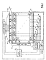
- FIG. 1 shows a liquid crystal display unit (LCD unit) 30 according to this embodiment.
- the LCD unit 30 comprises a driving device 32 as the driver for the liquid crystal display according to the present invention, and a reflective type liquid crystal display (LCD) 10 as the liquid crystal display.
- a driving device 32 as the driver for the liquid crystal display according to the present invention
- a reflective type liquid crystal display (LCD) 10 as the liquid crystal display.
- the LCD 10 comprises a pair of substrates 14 and 16 (the substrate 16 being transparent) oppositely disposed with a predetermined spacing by the spacer 12, between which liquid crystal 18 is sealed.
- a transparent electrode 20 is formed on the entire surface of the side of substrate 16 contacting the liquid crystal 18.
- Formed on the surface of substrate 14 contacting the liquid crystal 18 is a crystalline silicone layer on which a number of thin film transistors (TFTs) 24 are formed in a matrix (see Figure 2).
- An electrode 22 is provided in correspondence to each of TFTs 24.
- FIG 1 shows the circuit for LCD 10 in a simplified form. While illustration is omitted, the electrodes 22 are connected to the source of respective TFTs 24, and the liquid crystal 18 is held between the electrode 22 and the transparent electrode 20.
- the liquid crystal 18, the electrode 22, and the transparent electrode 20 for a single picture element are schematically shown by using the symbol for capacitor and with the reference "18" for the liquid crystal.
- the liquid crystal 18 corresponding to a single picture element constitutes a display cell of the present invention together with the electrode 22, the transparent electrode 20, and the TFT 24.
- the transparent electrode 20 is connected to a common terminal 26. In the embodiment, the common terminal 26 is grounded to make the potential of transparent electrode 20 constant (ground potential).
- the LCD 10 has m gate lines G1 - Gm extending along a predetermined direction toward the substrate 14.
- a gate of respective TFTs 24 is connected to any one of the gate lines G1 - Gm.
- Each of gate lines G1 - Gm is connected to a gate line driver 34 as gate line driving means, which is then connected to an LCD controller 36.
- n data lines d1A - dnA, d1B - dnB, d1C - dnC, and d1D - dnD extending in a direction intersecting the gate lines G1 - Gm.
- a drain of respective TFTs 24 is connected to any one of the data lines.
- the data lines are grouped into four data line groups d1A - dnA (data line group A), d1B - dnB (data line group B), d1C - dnC (data line group C), and d1D - dnD (data line group D) each of which consists of n data lines.
- each data line is connected to a multiplexer 38 having output terminals in the same number as total number of data lines (4 x n).
- the multiplexer 38 has n input terminals each of which is connected to a data line driver 40 through respective signal lines dl - dn.
- the data line driver 40 and the multiplexer 38 correspond to the data line driving means of the present invention.
- the data line driver 40 and the multiplexer 38 are connected to the LCD controller 36.
- each data line is connected to the source of respective transistors 42.
- n transistors connected to the data line group A d1A - dnA are called a "transistor group 42A”
- n transistors connected to the data line group B d1B - dnB are called a “transistor group 42B”
- n transistors connected to the data line group C d1C - dnC are called a “transistor group 42C”
- n transistors connected to the data line group D d1D - dnD are called a "transistor group 42D.”
- the gate of each transistor in the transistor groups 42A, 42B, 42C, and 42D is connected to a precharge controller 44 which is connected to the LCD controller 36.
- Each transistor 42 corresponds to the switching means of the present invention
- the precharge controller 44 corresponds to the ON/OFF control means of the present invention.
- each transistor in the transistor groups 42A, 42B, 42C, and 42D is connected to a voltage switching circuit 46.
- the voltage switching circuit 46 is connected to the LCD controller 36, and supplied with precharge voltages +V 1 and -V 1 .
- the voltage switching circuit 46 applies the precharge voltages +V 1 and -V 1 to the drain of the transistor according to an instruction from the LCD controller 36.
- the transistor groups 42A, 42B, 42C, 42D, the precharge controller 44, the voltage switching circuit 46, and the LCD controller 36 correspond to the potential control means of the present invention.
- the voltage switching circuit 46 corresponds to the potential changing means of the present invention.
- the precharge voltage +V 1 may be a value of one-half of the maximum value of data voltage which is described later, and the precharge voltage -V 1 may be a value of one-half of the minimum value of data voltage.
- the voltage switching circuit 46 is schematically shown as a switch in Figure 1, it actually includes a switching element such as a transistor.
- the LCD controller 36 controls the operation of the gate line driver 34 in such a manner that any one of m gate lines G1 - Gm is applied for a predetermined duration with a gate voltage turning on the TFT 24 connected to that gate line, and the gate lines applied with the gate voltage are sequentially changed over by the predetermined duration.
- the LCD controller 36 sequentially outputs image data representing gradation values to be displayed on each display cell in a display cell array connected to the gate line applied with the gate voltage to the data line driver 40 in synchronization with the timing in which the gate line driver 34 changes over the gate lines applied with the gate voltage.
- the data line driver 40 sequentially outputs image data for n display cells connected to a predetermined data line group from the input image data representing the gradation value to be displayed on each display cell, outputs voltage with magnitude corresponding to the gradation value represented by the taken-out image data (data voltage) to the multiplexer 38 through the signal lines dl - dn, and repeats these operations.
- the data line driver 40 outputs the data voltage to be applied to the display cells connected to each data line group to the multiplexer 38 in an order from the data line group A.
- the multiplexer 38 applies the data voltage output from the data line driver 40 to respective data lines of the corresponding data line group.
- the data voltage is applied to the data line groups A - D in this order within the duration when the gate voltage is applied to a predetermined gate line.
- the data voltage is then applied between an electrode pair consisting of the electrode 22 and the transparent electrode 20 of respective display cells for which TFT 24 is turned on.
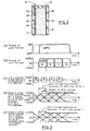
- the polarity of data voltage it may be acceptable to, as shown in Figure 4 (A), apply a data voltage with the same polarity to all display cells of the LCD when displaying the image of a frame, and to reverse the polarity of data voltage every one frame, or to, as shown in Figure 4 (B), apply a data voltage with the same polarity to an array of display cells connected to a same gate line when displaying the image of a frame, to reverse the polarity of data voltage every gate line, and, for the next frame, to apply a data voltage with polarity different from that of data voltage applied the previous time to each display cell array.
- the LCD controller 36 changes over the voltage switching circuit 46 in such a manner that, if the polarity of data voltage applied to each data line through the data line driver 40 and the multiplexer 38 is positive, the precharge voltage +V 1 is applied to the drain of each transistor in the transistor groups 42A - 42D, and, if the polarity of data voltage applied to each data line is negative, the precharge voltage -V 1 is applied to the drain of each transistor. That is, when the polarity of data voltage is reversed every one image frame as shown in Figure 4 (A), the precharge voltage is also switched every one image frame, and when the polarity of data voltage is reversed every one gate line as shown in Figure 4 (B), the precharge voltage is also switched every one gate line.
- the LCD controller 36 sequentially turns on the transistor groups 42A - 42D connected to the data line groups A - D through the precharge controller 44 at the timing shown in Figure 3 (C).
- a precharge voltage (+V 1 or -V 1 ) with the same polarity as that of the data voltage applied next time is applied to a data line before application of data voltage by the data line groups A - D. Therefore, if the data voltage is applied through the data line driver 40 and the multiplexer 38, the potential on each data line is changed to a value substantially equal to the applied precharge voltage, or a value close to the data voltage applied next time (an average value of data voltage being applied if the range of data voltage is +2.5 V - -2.5 V, and the precharge voltage is +1.25 V or -1.25 V).
- the precharge voltage is applied to the data line groups B - D, also as shown in Figure 3 (A), because the gate voltage is applied to the gate line, and the TFT 24 of each display cell in the display cell array connected to the gate line is turned on, the precharge voltage is applied between the electrode pair for the display cell in the display cell array connected to any one of respective data lines in the data line groups B - D, and the voltage between the electrode pair of the display cell substantially matches the precharge voltage when the data voltage is applied.
- the transistors in the transistor group A are turned on when the gate voltage is not applied to the gate line, it is not limited to such approach.
- Figure 3 (A) with imaginary lines it is allowed that the gate voltage is applied to the gate line even when each transistor in the transistor group 42A is turned on by advancing the timing to start application of the gate voltage to the gate line.
- the voltage between the electrode pair would be caused to be substantially equal to the precharge voltage when the data voltage is applied, the time is more reduced from the time when it is started to apply the data voltage to the time when the voltage between the electrode pair matches the data voltage, which is preferable.
- each data line and the voltage between the electrode pair of each display cell applied with the data voltage are +V 1
- the potential on the data line is -V 1 so that it becomes possible to reduce the amplitude of data voltage to be driven by the data line driver 40 (if it is assumed that the maximum value of the data voltage is +2.5 V, the minimum value is -2.5 V, and the precharge voltage V 1 is ⁇ 1.25 V, the amplitude can be made +2.5 V - 1.25 V to -2.5 V + 1.25 V, or +1.25 V to -1.25V).
- the transistors in each of the transistor groups 42A - 42D are turned on at different timing with each other, it is not limited to such approach.
- the gate voltage is preferably applied to the gate line as shown in Figure 3 (A) with imaginary lines.
- the voltage switching circuit 46 is omitted from the driving device 50 according to the second embodiment.
- the drain of each of transistors in the transistor groups 42A, 42B, 42C, and 42D is grounded through the terminal 48.
- wiring connecting the drain of each transistor and the grounding terminal corresponds to the potential control means of the present invention.
- the data line driver 40 changes over the polarity of data voltage as shown in Figure 4 (B) to display an image on the LCD 10.
- the precharge controller 44 sequentially turns on the transistor groups 42A - 42D connected to the data line groups A - D in this order in the timing shown in Figure 3 (C).
- the polarity of data voltage is changed over as shown in Figure 4 (B)
- the polarity of data voltage applied on respective data line is reversed every time.
- the data line connected to at least the turned on transistor has the potential of zero volt (ground potential). Accordingly, the potential on each data line when the data voltage is applied would be a value close to the data voltage being applied (more particularly, the maximum absolute value of the data voltage to be allied).
- the voltage between the electrode pair is also made zero volt for the display cell connected to any data line of the data line groups B - D of the display cell array. Since the polarity of data voltage applied to respective display cell is reversed every time, the voltage between the electrode pair of each display cell connected to the data line groups B - D is changed to a value close to the data value being applied when the data voltage is applied through the data line driver 40 and the multiplexer 38.
- all transistors in the transistor groups 42A - 42D may be turned on.
- the gate voltage is preferably applied to the gate line as shown in Figure 3 (A) with imaginary lines.
- the terminal 48 is grounded in the above, instead the terminal 48 may be applied with a constant voltage.
- the maximum absolute value of data voltage depends on the polarity of data voltage
- the time from starting the data voltage application to the data line until the voltage between the electrode pair of the display cell reaches a value corresponding to the value of gradation to be displayed on the display cell can be made constant regardless of the polarity of data voltage being applied.
- the drains of transistors in the transistor groups 42A, 42B, 42C, and 42D the sources of which are connected to the respective odd-numbered data lines in the data line groups A, B, C, and D (that is, data lines d1A, d3A, ... d1B, d3B, ... d1C, d3C, ...
- d1D, d3D, ...) are connected to a power supply line 54A, while the drains of transistors the sources of which are connected to the respective even-numbered data lines in the data line groups A, B, C, and D (that is, d2A, d4A, ... d2B, d4B, ... d2C, d4C, ... d2D, d4D, ...) are connected to the power supply line 54B.
- the power supply lines 54A and 54B are connected to the voltage switching circuit 46.
- the voltage switching circuit 46 applies the precharge voltage +V 1 or -V 1 to the power supply lines 54A and 54B according to an instruction from the LCD controller 36.
- the polarities of the precharge voltage the voltage switching circuit 46 applies to the power supply lines 54A and 54B are different each other. Then, when the precharge voltage +V 1 is applied to the power supply line 54A, the precharge voltage -V 1 is applied to the power supply line 54B, and when the precharge voltage -V 1 is applied to the power supply line 54A, the precharge voltage +V 1 is applied to the power supply line 54B.
- the power supply lines 54A and 54B, and the voltage switching circuit 46 correspond to the potential changing means of the present invention.
- the data line driver 40 applies the data voltage with polarity different each other to the odd-numbered data lines and the even-numbered data lines in the data line groups A, B, C, and D (see Figure 4 (C) or (D)).
- the polarity of the data voltage applied to each data line may be reversed every one gate line as shown in Figure 4 (C), or reversed every one image frame as shown in Figure 4 (D).
- the LCD controller 36 changes over the voltage switching circuit 46 in such a manner that, if the polarity of the data voltage applied to the odd-numbered data lines in the data line groups A, B, C, and D through the data line driver 40 and the multiplexer 38 is positive (that is, the polarity of the data voltage applied to the even-numbered data lines is negative), the precharge voltage +V 1 is applied to the power supply line 54A and the precharge voltage -V 1 is applied to the power supply line 54B, and that, if the polarity of the data voltage applied to the odd-numbered data lines is negative (that is, the polarity of the data voltage applied to the even-numbered data lines is positive), the precharge voltage -V 1 is applied to the power supply line 54A and the precharge voltage +V 1 is applied to the power supply line 54B.
- the operation of the voltage switching circuit 46 is controlled in such a manner that the polarity of the precharge voltage applied to the power supply lines 54A and 54B is also changed over every one gate line.
- the operation of the voltage switching circuit 46 is controlled in such a manner that the polarity of the precharge voltage applied to the power supply lines 54A and 54B is also changed over every one image frame.
- the LCD controller 36 sequentially turns on the transistor groups 42A - 42D connected to the data line groups A - D through the precharge controller 44 at the timing shown in Figure 3 (C).
- the precharge voltage with the same polarity as the data voltage applied to each data line next time (+V 1 or -V 1 ) is applied to each of the data line groups A - D.
- the potential on each data line when the data voltage is applied is changed to a value close to the data voltage being applied (for example, when the data voltage ranges +2.5 V - -2.5 V, and the precharge voltage is +1.25 V or -1.25 V, a value close to the average value of the data voltage being applied)
- the precharge voltage is applied between the electrode pair for a display cell connected to any one of data lines in the data line groups B - D, and, when the data voltage is applied, the voltage between the electrode pair of the display cell becomes a value substantially matching the precharge voltage.
- the gate voltage is applied to the gate line even when each transistor in the transistor group 42A is turned on by advancing the timing to start application of the gate voltage to the gate line. It may be also possible that all transistors in the transistor groups 42A - 42D are simultaneously turned on at the timing shown in Figure 3 (C) when the transistor group 42A is turned on. In such case, it is needless to say that the gate voltage is preferably applied to the gate line as shown in Figure 3 (A) with imaginary lines.
- the fourth embodiment of the present invention is explained. Components same as or similar to those of the third embodiment are attached with the same reference numerals and their description is omitted.
- the voltage switching circuit 46 is omitted from the driving device 56 according to the fourth embodiment.
- the drains of transistors in the transistor groups 42A, 42B, 42C, and 42D are grounded through the grounding conductor 58.
- the grounding conductor 58 corresponds to the potential changing means of the present invention.
- the data line driver 40 according to the fourth embodiment applies, as in the third embodiment, the data voltage with polarity different each other to the odd-numbered data lines and the even-numbered data lines in the data line groups A, B, C, and D, and reverses the polarity of data voltage applied to each data line by every one gate line (see Figure 4 (C)).
- the LCD controller 36 sequentially turns on the transistor groups 42A - 42D connected to the data line groups A - D at the timing shown in Figure 3 (C).
- Figure 8 (B) schematically shows the transistor 42 and the data line driver 40, and the multiplexer 38 is omitted for illustration.
- the display cell to which the data voltage with negative potential is applied previous time has the voltage between the electrode pair of zero volt when the data voltage with positive polarity is applied next time, and a charging current flows until the polarity of the voltage between the electrode pair reaches a predetermined positive value. Therefore, the charges accumulated between the electrode pair of the display cell to which the data voltage is applied (and, charges accumulated in the data lines) are uselessly disposed. This is also true to the first to third embodiment described above.
- the fourth embodiment by turning on each transistor in the transistor groups 42A - 42D, charges move through the grounding conductor 58 so that the potential on the adjacent data lines (for the data line groups B - D, also the voltage between the electrode pair of a pair of display cells connected to the adjacent data lines, respectively) also becomes equal.
- the absolute values of potentials on the adjacent data lines are equal, no charge flows to the grounding terminal so that the potentials on the adjacent data lines can be made zero volt equally without wasting any electrical power.
- the electrical power consumed by driving the data line can be reduced by 50%.
- each data line is applied with the data voltage with magnitude corresponding to the value of gradation to be displayed on each display cell
- the potential on the data line when the transistor is turned on has a value corresponding to the magnitude of data voltage previously applied
- the absolute values of potentials on the adjacent data lines are not necessarily equal. If the absolute values of potentials on the adjacent data lines, when the transistor is turned on, charges (current) not contributing change of the potential on the data line (and, the voltage between the electrode pair of the display cell), although it is very small, flows from the grounding conductor 58 to the grounding terminal.
- the reduction of power consumption is slightly less than 50%, it is possible to make the potentials on the adjacent data lines (and, the voltage between the electrode pair of a pair of display cells connected to the adjacent data lines, respectively) zero volt equally consuming substantially no electrical power (disposing substantially no accumulated charge) by more effectively utilizing the charges accumulated on the data lines or between the electrode pair of the display cell than in the prior art so that the electrical power consumed by driving the data line can be significantly reduced.
- the voltage between the electrode pair of the data cell applied with the data voltage reaches a value corresponding to the data voltage before the data voltage application duration expires, and the light transmittance of the liquid crystal 18 of the display cell matches that of the value of gradation to be displayed on the display cell.
- an image can be displayed at high quality even when the multiplex ratio is high and the duration of application of the data voltage is short for each display cell.
- the gate voltage is applied to the gate line at the timing shown in Figure 3 (A) with imaginary lines so that the gate voltage has been applied to the gate line when the transistor group 42A is turned on. Then, the charge accumulated between the electrode pair of the display cell connected to the data line group A can be also effectively utilized when the data voltage is applied next time. All transistors in the transistor groups 42A - 42D may be turned on at the timing shown in Figure 3 (C) when the transistor group 42A - 42D is turned on. In such case, it is needless to say that the gate voltage is preferably applied to the gate line as shown in Figure 3 (A) with imaginary lines.
- the voltage between the electrode pair of each display cell can be changed to zero volt, or a value close to the data voltage being applied before the data voltage is applied to each display cell so that the power consumption can be reduced, and an image can be displayed at high quality even when the duration of application of the data voltage is short for each display cell.
- Figure 9 shows simulations on changes of voltage between the electrode pair in a case where the precharge voltage is not applied (shown by broken lines in Figure 9), and where it is charged 1.5 V or -1.5 V (shown by solid lines in Figure 9) when +3 V and -3 V which are the maximum and minimum values as the data voltage, respectively, are alternately applied to the driving device 32 described for the first embodiment.
- Figure 9 (B) is an enlarged view of the area surrounded by the broken lines in Figure 9 (A).
- the voltage between the electrode pair increases even when the data voltage is completed for application, but does not reach the data voltage (+3 V in this case) with a relatively steep inclination of the increase of the voltage between the electrode pair.
- the insufficient amount of the voltage between the electrode pair to the data voltage corresponds to the difference of voltage between the electrode pair when the value of gradation differs by "1" in this embodiment although depending on the number of gradations to be displayed on the LCD 10.
- the present invention is not limited to such arrangement. It is needless to say that the data lines constituting each data line group may be divided into two groups, and data voltages with polarities different each other are applied to respective groups.
- the potential on the data line and, the voltage between the electrode pair of display cell
- the potential on the data line and the voltage between the electrode pair of the display cell may be precharged to a constant value corresponding to the maximum or minimum value of the data voltage by applying a constant voltage corresponding to the maximum or minimum value of the voltage between the electrode pair of the display cell (for example, +2.5 V or -2.5 V) to the data line while the gate voltage is applied to the gate line.
- a constant voltage corresponding to the maximum or minimum value of the voltage between the electrode pair of the display cell for example, +2.5 V or -2.5 V
- the data line driver can change the voltage between the electrode pair to a desired polarity and magnitude only by always applying a voltage with a constant polarity to the data line to change the voltage between the electrode pair to a fixed direction (for example, changing the voltage between the electrode pair toward the minimum value when the voltage between the electrode pair is precharged to the maximum value, or changing the voltage between the electrode pair toward the maximum value when the voltage between the electrode pair is precharged to the minimum value) so that it becomes possible to simplify the arrangement of the data line driver.
- the present invention is not limited to it, and may be used for a transmission type LCD.
- the transmission type LCD because it is impossible to use crystal silicon with very low light transmittance as in the reflective type LCD 10 as the substrate material for forming switching elements such as TFT, a substrate consisting of amorphous silicon or polysilicon is used.
- a substrate consisting of amorphous silicon or polysilicon is used.
- logic circuits such as the multiplexer on such substrate of amorphous silicon or polysilicon when compared with the formation on the crystal silicon substrate. Therefore, if it is assumed to perform multiplex driving, it is desirable to apply the present invention to driving of a reflective type LCD.
- the present invention is not limited to it, but may be applied to a conventional driving system where the data voltage is applied to all data lines at the same timing.
Landscapes
- Physics & Mathematics (AREA)
- Engineering & Computer Science (AREA)
- General Physics & Mathematics (AREA)
- Crystallography & Structural Chemistry (AREA)
- Chemical & Material Sciences (AREA)
- Theoretical Computer Science (AREA)
- Computer Hardware Design (AREA)
- Nonlinear Science (AREA)
- Mathematical Physics (AREA)
- Optics & Photonics (AREA)
- Liquid Crystal Display Device Control (AREA)
- Liquid Crystal (AREA)
- Control Of Indicators Other Than Cathode Ray Tubes (AREA)
Claims (11)
- Steuervorrichtung zum Ansteuern einer Flüssigkristallanzeige (10), an welche die Steuervorrichtung angeschlossen werden kann, wobei in der Flüssigkristallanzeige eine Anzahl Datenleitungen (d1..dn) und eine Anzahl Steuerleitungen (G1..Gm) so angeordnet sind, dass sie sich gegenseitig kreuzen, und an den Kreuzungspunkten der Daten- und der Steuerleitungen entsprechende Anzeigezellen (18) angeordnet sind und wobei die Datenleitungen aus einer Vielzahl von Datenleitungsgruppen (A, B, C, D) bestehen, jede Anzeigezelle ein mit einer Datenleitung und einer Steuerleitung verbundenes Schaltelement (24), ein einen Pixelkondensator bildendes in einem vorgegebenen Abstand gegenüber liegendes Elektrodenpaar (22, 20) und einen zwischen dem Elektrodenpaar angeordneten Flüssigkristall (18) umfasst, wobei die Steuervorrichtung Folgendes umfasst:dadurch gekennzeichnet, dass die Steuervorrichtung ferner Folgendes umfasst:ein Steuerleitungssteuermittel (34), das zum Anlegen einer Spannung an die Steuerleitungen mit einer Anzahl der Steuerleitungen verbunden werden kann, um das Schaltelement der mit der Steuerleitung verbundenen Anzeigezelle für eine vorgegebene Zeitdauer einzuschalten; undein Datenleitungssteuermittel (40), das zum Anlegen einer Datenspannung an die Datenleitungen in jeder Datenleitungsgruppe für eine vorgegebene Zeitdauer mit einer Anzahl der Datenleitungen verbunden werden kann, um die Spannung zwischen dem Elektrodenpaar der mit derjenigen Steuerleitung verbundenen Anzeigezelle zu ändern, an welche durch das Steuerleitungssteuermittel die Spannung auf einen vorgegebenen Spannungswert angelegt wird;Potenzialsteuermittel (42A, 42B, 42C, 42D, 44, 46, 36) zur Steuerung des Potenzials einer Anzahl von Datenleitungen in der Weise, dass das Potenzial der Datenleitung in jeder Datenleitungsgruppe vor dem Anlegen der Datenspannung durch das Datenleitungssteuermittel an die Datenleitung in jeder Datenleitungsgruppe so gesteuert wird, dass die Ladedauer für die Datenleitung und den Pixelkondensator verkürzt und das Potenzial an den Datenleitungen jeweils nur an einer Datenleitungsgruppe gesteuert wird.
- Steuervorrichtung zum Ansteuern einer Flüssigkristallanzeige (10) nach Anspruch 1, wobei das Potenzialsteuermittel ein Mittel zur Steuerung des Potenzials an den Datenleitungen (d1..dn) enthält, sodass das Potenzial an den Datenleitungen den Mittelwert der durch das Datenleitungssteuermittel (40) angelegten Datenspannung oder den minimalen Absolutwert der Datenspannung annimmt.
- Steuervorrichtung zum Ansteuern einer Flüssigkristallanzeige (10) nach Anspruch 1 oder Anspruch 2, wobei das Datenleitungssteuermittel (40) ein Mittel zum Anlegen einer Spannung an eine erste Teilgruppe der Datenleitungen (d1..dn) enthält, deren Polarität sich von der Polarität der an die Datenleitungen außer der ersten Teilgruppe von Datenleitungen angelegten Spannung unterscheidet, und wobei das Potenzialsteuermittel ein Mittel zur Steuerung des Potenzials an den Datenleitungen durch elektrisches Verbinden jeder Datenleitung der ersten Teilgruppe mit Datenleitungen außer der ersten Teilgruppe von Datenleitungen enthält.
- Steuervorrichtung zum Ansteuern einer Flüssigkristallanzeige (10) nach einem der Ansprüche 1 bis 3, wobei das Potenzialsteuermittel jede aus einer Anzahl von Datenleitungen (d1..dn) während des Zeitraums vom Anlegen der Datenspannung an die Datenleitung durch das Datenleitungssteuermittel (40) zu einem früheren Zeitpunkt bis zum nächsten Anlegen der Datenspannung steuert.
- Steuervorrichtung zum Ansteuern einer Flüssigkristallanzeige (10) nach Anspruch 4, wobei das Potenzialsteuermittel das Potenzial an den Datenleitungen (d1..dn) während des Zeitraums steuert, während dessen eine Spannung an der Steuerleitung anliegt, die mit einer Anzeigezelle (18) verbunden ist, deren Spannung zwischen dem Elektrodenpaar durch die an die Datenleitung anzulegende Datenspannung geändert werden soll.
- Steuervorrichtung zum Ansteuern einer Flüssigkristallanzeige (10) nach einem der Ansprüche 1 bis 5, wobei das Potenzialsteuermittel Folgendes umfasst:ein Potenzialänderungsmittel (46) zum Ändern des Potenzials an den Datenleitungen;eine Anzahl zwischen dem Potenzialänderungsmittel und einer Anzahl von Datenleitungen angeordnetes Schaltmittel (42A, 42B, 42C, 42D); undein EIN/AUS-Schaltmittel (44) zum Steuern des Ein-/Ausschaltens jedes aus der Anzahl von Schaltmitteln.
- Steuerverfahren zum Ansteuern einer Flüssigkristallanzeige (10), bei der eine Anzahl von Datenleitungen (d1..dn) und eine Anzahl von Steuerleitungen (G1..Gm) so angeordnet sind, dass sie sich gegenseitig kreuzen, und an den Kreuzungspunkten der Daten- und der Steuerleitungen entsprechende Anzeigezellen (18) angeordnet sind und wobei die Datenleitungen aus einer Vielzahl von Datenleitungsgruppen (A, B, C, D) bestehen, jede Anzeigezelle aus einem mit einer Datenleitung und einer Steuerleitung verbundenes Schaltelement (24), einem einen Pixelkondensator bildenden in einem vorgegebenen Abstand gegenüberliegenden Elektrodenpaar und einem zwischen dem Elektrodenpaar (22, 20) angeordneten Flüssigkristall besteht, wobei das Verfahren die folgenden Schritte umfasst:dadurch gekennzeichnet, dass das Verfahren ferner die folgenden Schritte umfasst:Anlegen einer Spannung an die Steuerleitungen, um das Schaltelement der mit der Steuerleitung verbundenen Anzeigezelle für eine vorgegebene Zeitdauer einzuschalten; undAnlegen einer Datenspannung an die Datenleitung während der vorgegebenen Zeitdauer zum Ändern einer Spannung zwischen dem Elektrodenpaar der Anzeigezelle, welche mit der Steuerleitung verbunden ist, an welche die Spannung durch das Steuerleitungssteuermittel auf einen vorgegebenen Spannungswert angelegt wird;Steuern des Potenzial an der Datenleitung in der Weise, dass das Potenzial an der Datenleitung vor dem Schritt des Anlegens einer Datenspannung so gesteuert wird, dass die Ladedauer für die Datenleitung und den Pixelkondensator verkürzt und das Potenzial an den Datenleitungen jeweils nur an einer Datenleitungsgruppe gesteuert wird.
- Steuerverfahren zum Ansteuern einer Flüssigkristallanzeige (10) nach Anspruch 7, wobei der Steuerschritt das Potenzial an den Datenleitungen (d1..dn) in der Weise steuert, dass das Potenzial an den Datenleitungen den Mittelwert der Datenspannung oder den minimalen Absolutwert der Datenspannung annimmt.
- Steuerverfahren zum Ansteuern einer Flüssigkristallanzeige (10) nach Anspruch 7 oder Anspruch 8, wobei der Schritt des Anlegens der Datenspannung an die erste Teilgruppe der Datenleitungen eine Spannung mit einer Polarität anlegt, die sich von der Polarität der an die Datenleitungen außer der ersten Teilgruppe von Datenleitungen angelegten Spannung unterscheidet; und
wobei der Steuerschritt das Potenzial an der Datenleitung durch elektrisches Verbinden jeder Datenleitung der ersten Teilgruppe der Datenleitungen mit Datenleitungen außer der ersten Teilgruppe der Datenleitungen steuert. - Steuerverfahren zum Ansteuern einer Flüssigkristallanzeige (10) nach einem der Ansprüche 7 bis Anspruch 9, wobei der Steuerschritt während des Zeitraums nach dem Anlegen der Datenspannung an die Datenleitung (d1..dn) zu einem früheren Zeitpunkt bis zum nächsten Anlegen der Datenspannung ausgeführt wird.
- Steuerverfahren zum Ansteuern einer Flüssigkristallanzeige (10) nach Anspruch 10, wobei der Steuerschritt ausgeführt wird, während eine Spannung an der Steuerleitung (G1..Gm) einer Anzeigezelle (18) anliegt, deren Spannung zwischen dem Elektrodenpaar durch die an die Datenleitung angelegte Datenspannung geändert werden soll.
Applications Claiming Priority (3)
| Application Number | Priority Date | Filing Date | Title |
|---|---|---|---|
| JP18138995 | 1995-07-18 | ||
| JP181389/95 | 1995-07-18 | ||
| JP07181389A JP3110980B2 (ja) | 1995-07-18 | 1995-07-18 | 液晶表示装置の駆動装置及び方法 |
Publications (2)
| Publication Number | Publication Date |
|---|---|
| EP0755044A1 EP0755044A1 (de) | 1997-01-22 |
| EP0755044B1 true EP0755044B1 (de) | 2003-09-17 |
Family
ID=16099891
Family Applications (1)
| Application Number | Title | Priority Date | Filing Date |
|---|---|---|---|
| EP96304946A Expired - Lifetime EP0755044B1 (de) | 1995-07-18 | 1996-07-04 | Verfahren und Einrichtung zur Steuerung einer Flüssigkristallanzeige mit Vorladen von Anzeigedatenleitungen |
Country Status (6)
| Country | Link |
|---|---|
| US (1) | US5892493A (de) |
| EP (1) | EP0755044B1 (de) |
| JP (1) | JP3110980B2 (de) |
| KR (1) | KR100245965B1 (de) |
| DE (1) | DE69629985T2 (de) |
| TW (1) | TW300301B (de) |
Families Citing this family (121)
| Publication number | Priority date | Publication date | Assignee | Title |
|---|---|---|---|---|
| JPH09152847A (ja) * | 1995-09-29 | 1997-06-10 | Sharp Corp | 液晶表示パネルの駆動方法及びその駆動回路 |
| FR2743658B1 (fr) * | 1996-01-11 | 1998-02-13 | Thomson Lcd | Procede d'adressage d'un ecran plat utilisant une precharge des pixels circuit de commande permettant la mise en oeuvre du procede et son application aux ecrans de grandes dimensions |
| JP3349638B2 (ja) | 1996-11-15 | 2002-11-25 | シャープ株式会社 | 表示装置を駆動する方法および回路 |
| KR100242110B1 (ko) * | 1997-04-30 | 2000-02-01 | 구본준 | 도트인버전 구동방식의 액정표시장치와 그 구동회로 |
| JP4308162B2 (ja) * | 1997-05-13 | 2009-08-05 | Okiセミコンダクタ株式会社 | 液晶表示装置の駆動回路及びその駆動方法 |
| KR100430091B1 (ko) * | 1997-07-10 | 2004-07-15 | 엘지.필립스 엘시디 주식회사 | 액정표시장치 |
| JP3704716B2 (ja) * | 1997-07-14 | 2005-10-12 | セイコーエプソン株式会社 | 液晶装置及びその駆動方法、並びにそれを用いた投写型表示装置及び電子機器 |
| CA2302230C (en) * | 1997-09-04 | 2004-11-16 | Silicon Image, Inc. | Power saving circuit and method for driving an active matrix display |
| US6243062B1 (en) * | 1997-09-23 | 2001-06-05 | Ois Optical Imaging Systems, Inc. | Method and system for addressing LCD including thin film diodes |
| JP4232227B2 (ja) * | 1998-03-25 | 2009-03-04 | ソニー株式会社 | 表示装置 |
| US6496172B1 (en) * | 1998-03-27 | 2002-12-17 | Semiconductor Energy Laboratory Co., Ltd. | Liquid crystal display device, active matrix type liquid crystal display device, and method of driving the same |
| KR19990081022A (ko) * | 1998-04-24 | 1999-11-15 | 윤종용 | 소비전력을 줄이기 위한 액정표시장치 구동회로 |
| TW530287B (en) | 1998-09-03 | 2003-05-01 | Samsung Electronics Co Ltd | Display device, and apparatus and method for driving display device |
| US6985142B1 (en) | 1998-09-03 | 2006-01-10 | University Of Southern California | Power-efficient, pulsed driving of capacitive loads to controllable voltage levels |
| AU5809999A (en) * | 1998-09-03 | 2000-03-27 | University Of Southern California | Power-efficient, pulsed driving of capacitive loads to controllable voltage levels |
| US6806862B1 (en) * | 1998-10-27 | 2004-10-19 | Fujitsu Display Technologies Corporation | Liquid crystal display device |
| KR100580550B1 (ko) * | 1998-12-09 | 2006-11-10 | 엘지.필립스 엘시디 주식회사 | 블록순차구동방법및그장치 |
| GB9827988D0 (en) * | 1998-12-19 | 1999-02-10 | Koninkl Philips Electronics Nv | Active matrix liquid crystal display devices |
| TW521241B (en) | 1999-03-16 | 2003-02-21 | Sony Corp | Liquid crystal display apparatus, its driving method, and liquid crystal display system |
| KR100295679B1 (ko) * | 1999-03-30 | 2001-07-12 | 김영환 | 티에프티 엘씨디 칼럼 구동 장치 및 그 구동 방법 |
| TW564388B (en) | 1999-05-11 | 2003-12-01 | Toshiba Corp | Method of driving flat-panel display device |
| KR100701892B1 (ko) | 1999-05-21 | 2007-03-30 | 엘지.필립스 엘시디 주식회사 | 데이터라인 구동방법 및 그를 이용한 액정 표시장치 |
| GB9917677D0 (en) * | 1999-07-29 | 1999-09-29 | Koninkl Philips Electronics Nv | Active matrix array devices |
| KR100344186B1 (ko) * | 1999-08-05 | 2002-07-19 | 주식회사 네오텍리서치 | 액정표시장치의 소오스 구동회로 및 그 구동방법 |
| TW501069B (en) * | 1999-08-18 | 2002-09-01 | Thomson Licensing Sa | Method of operating capacitive thin film transistor arrays |
| JP3782668B2 (ja) * | 2000-03-30 | 2006-06-07 | シャープ株式会社 | 画像表示装置およびその駆動方法 |
| JP3777913B2 (ja) * | 1999-10-28 | 2006-05-24 | 株式会社日立製作所 | 液晶駆動回路及び液晶表示装置 |
| US6750835B2 (en) * | 1999-12-27 | 2004-06-15 | Semiconductor Energy Laboratory Co., Ltd. | Image display device and driving method thereof |
| US7098884B2 (en) * | 2000-02-08 | 2006-08-29 | Semiconductor Energy Laboratory Co., Ltd. | Semiconductor display device and method of driving semiconductor display device |
| KR100699694B1 (ko) * | 2000-02-25 | 2007-03-26 | 엘지.필립스 엘시디 주식회사 | 액정표시장치 |
| JP2001343946A (ja) * | 2000-05-31 | 2001-12-14 | Alps Electric Co Ltd | 液晶表示装置およびその駆動方法 |
| KR100685942B1 (ko) * | 2000-08-30 | 2007-02-23 | 엘지.필립스 엘시디 주식회사 | 액정표시장치 및 그 구동방법 |
| JP3638121B2 (ja) * | 2000-10-19 | 2005-04-13 | シャープ株式会社 | データ信号線駆動回路およびそれを備える画像表示装置 |
| JP4929431B2 (ja) * | 2000-11-10 | 2012-05-09 | Nltテクノロジー株式会社 | パネル表示装置のデータ線駆動回路 |
| US7176482B1 (en) | 2000-11-28 | 2007-02-13 | Ramot At Tel-Aviv University | DNA-based electronics |
| EP1275103A4 (de) * | 2000-11-30 | 2008-11-12 | Thomson Licensing | Ansteuerschaltung zur verbesserten helligkeitsregelung in flüssigkristallanzeigen und verfahren hierfür |
| KR100698031B1 (ko) * | 2000-12-07 | 2007-03-23 | 엘지.필립스 엘시디 주식회사 | 접합 액정표시소자 및 그 구동 방법 |
| US6850218B2 (en) * | 2000-12-18 | 2005-02-01 | Brillian Corporation | Frame prewriting in a liquid crystal display |
| US7088330B2 (en) * | 2000-12-25 | 2006-08-08 | Sharp Kabushiki Kaisha | Active matrix substrate, display device and method for driving the display device |
| KR100759974B1 (ko) * | 2001-02-26 | 2007-09-18 | 삼성전자주식회사 | 액정 표시 장치 및 그의 구동 방법. |
| US6630921B2 (en) * | 2001-03-20 | 2003-10-07 | Koninklijke Philips Electronics N.V. | Column driving circuit and method for driving pixels in a column row matrix |
| JP2002297109A (ja) * | 2001-03-30 | 2002-10-11 | Fujitsu Ltd | 液晶表示装置及びその駆動回路 |
| JP2003084736A (ja) * | 2001-06-25 | 2003-03-19 | Nec Corp | 液晶表示装置 |
| JP4271414B2 (ja) * | 2001-09-25 | 2009-06-03 | シャープ株式会社 | 画像表示装置および表示駆動方法 |
| JP3642042B2 (ja) * | 2001-10-17 | 2005-04-27 | ソニー株式会社 | 表示装置 |
| US20030085856A1 (en) * | 2001-11-02 | 2003-05-08 | Klein Terence R | System and method for minimizing image degradation in LCD microdisplays |
| KR100864918B1 (ko) | 2001-12-26 | 2008-10-22 | 엘지디스플레이 주식회사 | 액정표시장치의 데이터 구동 장치 |
| KR100421053B1 (ko) * | 2002-02-22 | 2004-03-04 | 삼성전자주식회사 | 신호선의 프리차지 방법 및 프리차지 전압발생회로 |
| JP3820379B2 (ja) * | 2002-03-13 | 2006-09-13 | 松下電器産業株式会社 | 液晶駆動装置 |
| JP4154911B2 (ja) * | 2002-03-29 | 2008-09-24 | 松下電器産業株式会社 | 液晶表示装置の駆動方法と液晶表示装置 |
| JP2003323160A (ja) | 2002-04-30 | 2003-11-14 | Sony Corp | 液晶表示装置およびその駆動方法、ならびに携帯端末 |
| JP4103544B2 (ja) * | 2002-10-28 | 2008-06-18 | セイコーエプソン株式会社 | 有機el装置 |
| KR100487808B1 (ko) * | 2002-12-10 | 2005-05-06 | 엘지.필립스 엘시디 주식회사 | 그라인딩 공정 전의 액정표시패널 및 액정표시패널의 제조 방법 |
| US8487859B2 (en) * | 2002-12-30 | 2013-07-16 | Lg Display Co., Ltd. | Data driving apparatus and method for liquid crystal display device |
| KR100697378B1 (ko) * | 2003-03-10 | 2007-03-20 | 비오이 하이디스 테크놀로지 주식회사 | 액정표시장치 및 그 구동방법 |
| JP3882796B2 (ja) * | 2003-07-22 | 2007-02-21 | セイコーエプソン株式会社 | 電気光学装置、電気光学装置の駆動方法および電子機器 |
| JP4144474B2 (ja) | 2003-08-22 | 2008-09-03 | ソニー株式会社 | 画像表示装置、画像表示パネル、パネル駆動装置および画像表示パネルの駆動方法 |
| JP4176688B2 (ja) | 2003-09-17 | 2008-11-05 | シャープ株式会社 | 表示装置およびその駆動方法 |
| JP4521176B2 (ja) * | 2003-10-31 | 2010-08-11 | 東芝モバイルディスプレイ株式会社 | 表示装置 |
| JP4385730B2 (ja) * | 2003-11-13 | 2009-12-16 | セイコーエプソン株式会社 | 電気光学装置の駆動方法、電気光学装置および電子機器 |
| KR100578911B1 (ko) * | 2003-11-26 | 2006-05-11 | 삼성에스디아이 주식회사 | 전류 역다중화 장치 및 이를 이용한 전류 기입형 표시 장치 |
| KR100578913B1 (ko) * | 2003-11-27 | 2006-05-11 | 삼성에스디아이 주식회사 | 역다중화기를 이용한 표시 장치 및 그 구동 방법 |
| KR100578914B1 (ko) * | 2003-11-27 | 2006-05-11 | 삼성에스디아이 주식회사 | 역다중화기를 이용한 표시 장치 |
| KR100589381B1 (ko) * | 2003-11-27 | 2006-06-14 | 삼성에스디아이 주식회사 | 역다중화기를 이용한 표시 장치 및 그 구동 방법 |
| KR101057777B1 (ko) | 2003-12-26 | 2011-08-19 | 엘지디스플레이 주식회사 | 액정 표시 패널의 프리차징 방법 및 장치와 그를 이용한액정 패널 및 그 구동 방법 |
| JP2005195810A (ja) * | 2004-01-06 | 2005-07-21 | Nec Electronics Corp | 容量性負荷駆動回路、及び表示パネル駆動回路 |
| KR101126343B1 (ko) * | 2004-04-30 | 2012-03-23 | 엘지디스플레이 주식회사 | 일렉트로-루미네센스 표시장치 |
| KR100600350B1 (ko) * | 2004-05-15 | 2006-07-14 | 삼성에스디아이 주식회사 | 역다중화 및 이를 구비한 유기 전계발광 표시 장치 |
| KR100622217B1 (ko) * | 2004-05-25 | 2006-09-08 | 삼성에스디아이 주식회사 | 유기 전계발광 표시장치 및 역다중화부 |
| US20060012595A1 (en) * | 2004-07-19 | 2006-01-19 | Chien-Chih Chen | Driving circuit and driving process of display system |
| KR100581810B1 (ko) * | 2004-08-25 | 2006-05-23 | 삼성에스디아이 주식회사 | 발광 표시장치와 그의 구동방법 |
| US8199079B2 (en) * | 2004-08-25 | 2012-06-12 | Samsung Mobile Display Co., Ltd. | Demultiplexing circuit, light emitting display using the same, and driving method thereof |
| KR100640894B1 (ko) * | 2004-09-07 | 2006-11-02 | 엘지전자 주식회사 | 이동통신 단말기용 컬러 액정 표시 장치의 제어 장치 및 제어방법 |
| JP2006154772A (ja) * | 2004-10-25 | 2006-06-15 | Nec Micro Systems Ltd | 液晶表示装置、液晶ドライバ及びその動作方法 |
| KR100637203B1 (ko) * | 2005-01-07 | 2006-10-23 | 삼성에스디아이 주식회사 | 유기 전계발광 표시장치 및 그 동작방법 |
| JPWO2006075768A1 (ja) * | 2005-01-11 | 2008-06-12 | ローム株式会社 | 容量負荷駆動方法、容量負荷駆動装置、および液晶表示装置 |
| US7830352B2 (en) * | 2005-01-14 | 2010-11-09 | Au Optronics Corp. | Driving circuit for flat panel display which provides a horizontal start signal to first and second shift register cells |
| KR101152119B1 (ko) * | 2005-02-07 | 2012-06-15 | 삼성전자주식회사 | 표시 장치 및 그 구동 방법 |
| US8619007B2 (en) * | 2005-03-31 | 2013-12-31 | Lg Display Co., Ltd. | Electro-luminescence display device for implementing compact panel and driving method thereof |
| TWI297484B (en) * | 2005-04-01 | 2008-06-01 | Au Optronics Corp | Time division driven display and method for driving same |
| JP4400588B2 (ja) | 2005-06-02 | 2010-01-20 | エプソンイメージングデバイス株式会社 | 電気光学装置、電気光学装置の駆動方法、および、電子機器 |
| KR101147104B1 (ko) | 2005-06-27 | 2012-05-18 | 엘지디스플레이 주식회사 | 액정 표시 장치의 데이터 구동 방법 및 장치 |
| KR101167407B1 (ko) * | 2005-06-28 | 2012-07-19 | 엘지디스플레이 주식회사 | 액정표시장치와 그 구동방법 |
| DE102005039538A1 (de) * | 2005-08-20 | 2007-02-22 | Universität des Saarlandes | Verfahren und Schaltung zur Ansteuerung einer Anzeige |
| KR100740101B1 (ko) * | 2005-08-30 | 2007-07-16 | 삼성에스디아이 주식회사 | 유기 발광 표시 장치 및 그 구동 방법 |
| KR20070040505A (ko) * | 2005-10-12 | 2007-04-17 | 삼성전자주식회사 | 표시 장치 및 이의 검사 방법 |
| KR20070093540A (ko) * | 2006-03-14 | 2007-09-19 | 삼성전자주식회사 | 표시 장치 |
| CN100523824C (zh) * | 2006-03-15 | 2009-08-05 | 中华映管股份有限公司 | 检测线路布局以及液晶显示面板的制造方法 |
| TWI337451B (en) * | 2006-04-03 | 2011-02-11 | Novatek Microelectronics Corp | Method and related device of source driver with reduced power consumption |
| CN101059941B (zh) | 2006-04-17 | 2010-08-18 | 乐金显示有限公司 | 显示装置及其驱动方法 |
| KR100761109B1 (ko) * | 2006-05-19 | 2007-09-21 | 엘지전자 주식회사 | 전계발광표시장치와 그 구동방법 |
| KR101244656B1 (ko) * | 2006-06-19 | 2013-03-18 | 엘지디스플레이 주식회사 | 액정표시장치 |
| JP4501952B2 (ja) * | 2007-03-28 | 2010-07-14 | セイコーエプソン株式会社 | 電気光学装置、その駆動方法および電子機器 |
| JP2008268671A (ja) * | 2007-04-23 | 2008-11-06 | Canon Inc | 液晶表示装置、その制御方法及び液晶プロジェクタシステム |
| KR101510877B1 (ko) | 2007-06-20 | 2015-04-10 | 엘지디스플레이 주식회사 | 액정표시장치 및 그의 구동방법 |
| TWI352233B (en) * | 2007-08-21 | 2011-11-11 | Au Optronics Corp | Liquid crystal display with a precharge circuit |
| KR101604140B1 (ko) * | 2009-12-03 | 2016-03-17 | 엘지디스플레이 주식회사 | 액정표시장치 |
| TWI440001B (zh) * | 2010-02-24 | 2014-06-01 | Chunghwa Picture Tubes Ltd | 液晶顯示裝置及其驅動方法 |
| JP2012018320A (ja) * | 2010-07-08 | 2012-01-26 | Hitachi Displays Ltd | 表示装置 |
| CN102376238B (zh) * | 2010-08-16 | 2015-12-16 | 立景光电股份有限公司 | 显示装置、像素电路及像素电路的操作方法 |
| TWI455104B (zh) * | 2011-08-15 | 2014-10-01 | Innolux Corp | 藍相液晶顯示裝置及其驅動方法 |
| KR101920763B1 (ko) * | 2011-12-29 | 2019-02-14 | 엘지디스플레이 주식회사 | 표시장치 |
| TWI460709B (zh) * | 2012-07-03 | 2014-11-11 | Au Optronics Corp | 液晶顯示器及相關配向方法 |
| TWI466098B (zh) * | 2012-12-11 | 2014-12-21 | Novatek Microelectronics Corp | 顯示器驅動方法以及驅動電路 |
| KR101606874B1 (ko) * | 2012-12-28 | 2016-03-28 | 엘지디스플레이 주식회사 | 터치스크린 일체형 표시장치 및 그 구동 방법 |
| JP2014134685A (ja) | 2013-01-10 | 2014-07-24 | Japan Display Inc | 液晶表示装置 |
| KR20150033156A (ko) * | 2013-09-23 | 2015-04-01 | 삼성디스플레이 주식회사 | 표시 장치 및 그 구동 방법 |
| JP6314450B2 (ja) * | 2013-12-02 | 2018-04-25 | セイコーエプソン株式会社 | 電気光学装置、及び電子機器 |
| CN104036747A (zh) * | 2014-06-13 | 2014-09-10 | 深圳市华星光电技术有限公司 | 可减少驱动芯片的电子装置 |
| JP6488651B2 (ja) * | 2014-11-05 | 2019-03-27 | セイコーエプソン株式会社 | 電気光学装置、電気光学装置の制御方法および電子機器 |
| CN104880875B (zh) * | 2015-06-02 | 2019-08-30 | 深圳市华星光电技术有限公司 | 一种阵列基板和液晶显示面板 |
| JP2017167426A (ja) * | 2016-03-17 | 2017-09-21 | セイコーエプソン株式会社 | 電気光学装置、及び電子機器 |
| TWI645396B (zh) * | 2018-03-07 | 2018-12-21 | 友達光電股份有限公司 | 顯示面板及預充電方法 |
| CN109410857A (zh) * | 2018-11-12 | 2019-03-01 | 惠科股份有限公司 | 一种显示面板的跨压补偿方法、显示面板和显示装置 |
| CN109801585B (zh) * | 2019-03-25 | 2022-07-29 | 京东方科技集团股份有限公司 | 显示面板驱动电路及驱动方法、显示面板 |
| CN110211547A (zh) * | 2019-06-04 | 2019-09-06 | 京东方科技集团股份有限公司 | 一种显示面板、其驱动方法及显示装置 |
| CN110164396B (zh) * | 2019-06-12 | 2021-09-03 | 京东方科技集团股份有限公司 | 一种显示面板及其驱动方法、显示装置 |
| CN112242125B (zh) * | 2019-07-19 | 2023-08-18 | 深圳光峰科技股份有限公司 | 显示设备 |
| KR102675921B1 (ko) * | 2019-11-07 | 2024-06-17 | 엘지디스플레이 주식회사 | 표시 장치 및 표시 장치의 데이터 링크 라인 결함 검출 방법 |
| US11908366B2 (en) * | 2020-09-24 | 2024-02-20 | HKC Corporation Limited | Cross voltage compensation method for display panel, display panel and display device |
| WO2023240586A1 (zh) * | 2022-06-17 | 2023-12-21 | 京东方科技集团股份有限公司 | 显示面板的驱动方法、驱动电路、驱动芯片和显示设备 |
Family Cites Families (10)
| Publication number | Priority date | Publication date | Assignee | Title |
|---|---|---|---|---|
| AU588062B2 (en) * | 1985-10-16 | 1989-09-07 | Sanyo Electric Co., Ltd. | Lcd matrix alternating drive circuit |
| US5151689A (en) * | 1988-04-25 | 1992-09-29 | Hitachi, Ltd. | Display device with matrix-arranged pixels having reduced number of vertical signal lines |
| JPH055865A (ja) * | 1991-06-27 | 1993-01-14 | Fujitsu Ltd | 液晶表示装置 |
| JP2806098B2 (ja) * | 1991-10-09 | 1998-09-30 | 松下電器産業株式会社 | 表示装置の駆動方法 |
| FI91684C (fi) * | 1992-05-15 | 1994-07-25 | Planar International Oy Ltd | Menetelmä ja laitteisto elektroluminenssimatriisinäytön ohjaamiseksi |
| US5426447A (en) * | 1992-11-04 | 1995-06-20 | Yuen Foong Yu H.K. Co., Ltd. | Data driving circuit for LCD display |
| JPH06337400A (ja) * | 1993-05-31 | 1994-12-06 | Sharp Corp | マトリクス型表示装置及び駆動方法 |
| JP2674484B2 (ja) * | 1993-10-22 | 1997-11-12 | 松下電器産業株式会社 | アクティブマトリクス液晶表示装置 |
| JP3482683B2 (ja) * | 1994-04-22 | 2003-12-22 | ソニー株式会社 | アクティブマトリクス表示装置及びその駆動方法 |
| JP3451717B2 (ja) * | 1994-04-22 | 2003-09-29 | ソニー株式会社 | アクティブマトリクス表示装置及びその駆動方法 |
-
1995
- 1995-07-18 JP JP07181389A patent/JP3110980B2/ja not_active Expired - Lifetime
- 1995-09-21 TW TW084109923A patent/TW300301B/zh not_active IP Right Cessation
-
1996
- 1996-07-04 EP EP96304946A patent/EP0755044B1/de not_active Expired - Lifetime
- 1996-07-04 DE DE69629985T patent/DE69629985T2/de not_active Expired - Fee Related
- 1996-07-09 KR KR1019960027547A patent/KR100245965B1/ko not_active Expired - Lifetime
- 1996-07-17 US US08/683,738 patent/US5892493A/en not_active Expired - Lifetime
Also Published As
| Publication number | Publication date |
|---|---|
| JP3110980B2 (ja) | 2000-11-20 |
| KR970007780A (ko) | 1997-02-21 |
| TW300301B (de) | 1997-03-11 |
| EP0755044A1 (de) | 1997-01-22 |
| KR100245965B1 (ko) | 2000-03-02 |
| DE69629985D1 (de) | 2003-10-23 |
| JPH0933891A (ja) | 1997-02-07 |
| US5892493A (en) | 1999-04-06 |
| DE69629985T2 (de) | 2004-07-15 |
Similar Documents
| Publication | Publication Date | Title |
|---|---|---|
| US5892493A (en) | Data line precharging apparatus and method for a liquid crystal display | |
| JP3621982B2 (ja) | 薄膜トランジスタ液晶表示装置と駆動方法及び駆動装置 | |
| US6933910B2 (en) | Image display device and method thereof | |
| CN1071025C (zh) | 显示器 | |
| KR100234720B1 (ko) | Tft-lcd의 구동회로 | |
| KR100296673B1 (ko) | 엘씨디 디스플레이용 데이터 드라이버회로 | |
| KR100233899B1 (ko) | 액정패널 및 액정표시장치 | |
| JP3297986B2 (ja) | アクティブマトリクス表示装置及びその駆動方法 | |
| KR101026802B1 (ko) | 액정 표시 장치 및 그 구동 방법 | |
| US6011530A (en) | Liquid crystal display | |
| US20080079703A1 (en) | Method of driving the display device and display device | |
| JPH075852A (ja) | 液晶表示装置で漏話を除去する方法及び液晶表示装置 | |
| US20090279007A1 (en) | Liquid crystal display | |
| KR100549983B1 (ko) | 액정표시장치 및 그 구동방법 | |
| US7286107B2 (en) | Liquid crystal display | |
| KR20030083309A (ko) | 액정표시장치 | |
| JP4420620B2 (ja) | 画像表示装置 | |
| JP3960781B2 (ja) | アクティブマトリクス型表示装置 | |
| JP3063670B2 (ja) | マトリクス表示装置 | |
| JPH07318901A (ja) | アクティブマトリクス型液晶表示装置及びその駆動方法 | |
| KR20090066605A (ko) | 액정 표시장치 및 그의 구동방법 | |
| JP4144474B2 (ja) | 画像表示装置、画像表示パネル、パネル駆動装置および画像表示パネルの駆動方法 | |
| JP3957403B2 (ja) | 液晶表示装置およびその駆動方法 | |
| JP2004521397A (ja) | ディスプレイデバイスとその駆動方法 | |
| US20040263453A1 (en) | Liquid crystal display device and method of fabricating the same |
Legal Events
| Date | Code | Title | Description |
|---|---|---|---|
| PUAI | Public reference made under article 153(3) epc to a published international application that has entered the european phase |
Free format text: ORIGINAL CODE: 0009012 |
|
| AK | Designated contracting states |
Kind code of ref document: A1 Designated state(s): DE FR GB |
|
| 17P | Request for examination filed |
Effective date: 19970521 |
|
| 17Q | First examination report despatched |
Effective date: 20020522 |
|
| RTI1 | Title (correction) |
Free format text: DEVICE AND METHOD FOR DRIVING LIQUID CRYSTAL DISPLAY WITH PRECHARGE OF DISPLAY DATA LINES |
|
| RTI1 | Title (correction) |
Free format text: DEVICE AND METHOD FOR DRIVING LIQUID CRYSTAL DISPLAY WITH PRECHARGE OF DISPLAY DATA LINES |
|
| GRAH | Despatch of communication of intention to grant a patent |
Free format text: ORIGINAL CODE: EPIDOS IGRA |
|
| RTI1 | Title (correction) |
Free format text: DEVICE AND METHOD FOR DRIVING LIQUID CRYSTAL DISPLAY WITH PRECHARGE OF DISPLAY DATA LINES |
|
| GRAS | Grant fee paid |
Free format text: ORIGINAL CODE: EPIDOSNIGR3 |
|
| GRAA | (expected) grant |
Free format text: ORIGINAL CODE: 0009210 |
|
| AK | Designated contracting states |
Kind code of ref document: B1 Designated state(s): DE FR GB |
|
| REG | Reference to a national code |
Ref country code: GB Ref legal event code: FG4D |
|
| REF | Corresponds to: |
Ref document number: 69629985 Country of ref document: DE Date of ref document: 20031023 Kind code of ref document: P |
|
| ET | Fr: translation filed | ||
| PLBE | No opposition filed within time limit |
Free format text: ORIGINAL CODE: 0009261 |
|
| STAA | Information on the status of an ep patent application or granted ep patent |
Free format text: STATUS: NO OPPOSITION FILED WITHIN TIME LIMIT |
|
| 26N | No opposition filed |
Effective date: 20040618 |
|
| REG | Reference to a national code |
Ref country code: GB Ref legal event code: 732E |
|
| REG | Reference to a national code |
Ref country code: FR Ref legal event code: TP |
|
| PGFP | Annual fee paid to national office [announced via postgrant information from national office to epo] |
Ref country code: DE Payment date: 20070831 Year of fee payment: 12 |
|
| PGFP | Annual fee paid to national office [announced via postgrant information from national office to epo] |
Ref country code: GB Payment date: 20070727 Year of fee payment: 12 |
|
| PGFP | Annual fee paid to national office [announced via postgrant information from national office to epo] |
Ref country code: FR Payment date: 20070717 Year of fee payment: 12 |
|
| GBPC | Gb: european patent ceased through non-payment of renewal fee |
Effective date: 20080704 |
|
| PG25 | Lapsed in a contracting state [announced via postgrant information from national office to epo] |
Ref country code: DE Free format text: LAPSE BECAUSE OF NON-PAYMENT OF DUE FEES Effective date: 20090203 |
|
| REG | Reference to a national code |
Ref country code: FR Ref legal event code: ST Effective date: 20090331 |
|
| PG25 | Lapsed in a contracting state [announced via postgrant information from national office to epo] |
Ref country code: GB Free format text: LAPSE BECAUSE OF NON-PAYMENT OF DUE FEES Effective date: 20080704 |
|
| PG25 | Lapsed in a contracting state [announced via postgrant information from national office to epo] |
Ref country code: FR Free format text: LAPSE BECAUSE OF NON-PAYMENT OF DUE FEES Effective date: 20080731 |