EP0747948A2 - Procédé et dispositif de fabrication de microstructures auto-assemblantes - Google Patents
Procédé et dispositif de fabrication de microstructures auto-assemblantes Download PDFInfo
- Publication number
- EP0747948A2 EP0747948A2 EP96109018A EP96109018A EP0747948A2 EP 0747948 A2 EP0747948 A2 EP 0747948A2 EP 96109018 A EP96109018 A EP 96109018A EP 96109018 A EP96109018 A EP 96109018A EP 0747948 A2 EP0747948 A2 EP 0747948A2
- Authority
- EP
- European Patent Office
- Prior art keywords
- substrate
- blocks
- block
- silicon
- shaped
- Prior art date
- Legal status (The legal status is an assumption and is not a legal conclusion. Google has not performed a legal analysis and makes no representation as to the accuracy of the status listed.)
- Withdrawn
Links
- 238000000034 method Methods 0.000 title claims abstract description 130
- 239000000758 substrate Substances 0.000 claims abstract description 198
- 239000002002 slurry Substances 0.000 claims abstract description 45
- 239000012530 fluid Substances 0.000 claims abstract description 37
- XUIMIQQOPSSXEZ-UHFFFAOYSA-N Silicon Chemical compound [Si] XUIMIQQOPSSXEZ-UHFFFAOYSA-N 0.000 claims description 143
- 229910052710 silicon Inorganic materials 0.000 claims description 143
- 239000010703 silicon Substances 0.000 claims description 143
- JBRZTFJDHDCESZ-UHFFFAOYSA-N AsGa Chemical compound [As]#[Ga] JBRZTFJDHDCESZ-UHFFFAOYSA-N 0.000 claims description 127
- 229910001218 Gallium arsenide Inorganic materials 0.000 claims description 120
- XLYOFNOQVPJJNP-UHFFFAOYSA-N water Substances O XLYOFNOQVPJJNP-UHFFFAOYSA-N 0.000 claims description 25
- 239000000463 material Substances 0.000 claims description 18
- 239000007789 gas Substances 0.000 claims description 11
- IJGRMHOSHXDMSA-UHFFFAOYSA-N Atomic nitrogen Chemical compound N#N IJGRMHOSHXDMSA-UHFFFAOYSA-N 0.000 claims description 9
- 230000000295 complement effect Effects 0.000 claims description 9
- 238000001465 metallisation Methods 0.000 claims description 9
- CSCPPACGZOOCGX-UHFFFAOYSA-N Acetone Chemical compound CC(C)=O CSCPPACGZOOCGX-UHFFFAOYSA-N 0.000 claims description 8
- 230000032258 transport Effects 0.000 claims description 8
- LFQSCWFLJHTTHZ-UHFFFAOYSA-N Ethanol Chemical compound CCO LFQSCWFLJHTTHZ-UHFFFAOYSA-N 0.000 claims description 7
- 239000011521 glass Substances 0.000 claims description 5
- 239000002985 plastic film Substances 0.000 claims description 5
- 229910052757 nitrogen Inorganic materials 0.000 claims description 4
- 239000004065 semiconductor Substances 0.000 claims description 4
- 239000000919 ceramic Substances 0.000 claims description 3
- 239000000243 solution Substances 0.000 description 60
- 238000005530 etching Methods 0.000 description 55
- 235000012431 wafers Nutrition 0.000 description 47
- VYPSYNLAJGMNEJ-UHFFFAOYSA-N Silicium dioxide Chemical compound O=[Si]=O VYPSYNLAJGMNEJ-UHFFFAOYSA-N 0.000 description 32
- 238000002474 experimental method Methods 0.000 description 29
- KRHYYFGTRYWZRS-UHFFFAOYSA-N Fluorane Chemical compound F KRHYYFGTRYWZRS-UHFFFAOYSA-N 0.000 description 27
- 229910004205 SiNX Inorganic materials 0.000 description 24
- MDPILPRLPQYEEN-UHFFFAOYSA-N aluminium arsenide Chemical compound [As]#[Al] MDPILPRLPQYEEN-UHFFFAOYSA-N 0.000 description 21
- KWYUFKZDYYNOTN-UHFFFAOYSA-M Potassium hydroxide Chemical compound [OH-].[K+] KWYUFKZDYYNOTN-UHFFFAOYSA-M 0.000 description 20
- 229920002120 photoresistant polymer Polymers 0.000 description 20
- OKKJLVBELUTLKV-UHFFFAOYSA-N Methanol Chemical compound OC OKKJLVBELUTLKV-UHFFFAOYSA-N 0.000 description 18
- 238000001451 molecular beam epitaxy Methods 0.000 description 18
- 238000004519 manufacturing process Methods 0.000 description 17
- QPJSUIGXIBEQAC-UHFFFAOYSA-N n-(2,4-dichloro-5-propan-2-yloxyphenyl)acetamide Chemical compound CC(C)OC1=CC(NC(C)=O)=C(Cl)C=C1Cl QPJSUIGXIBEQAC-UHFFFAOYSA-N 0.000 description 17
- 239000000377 silicon dioxide Substances 0.000 description 16
- MHAJPDPJQMAIIY-UHFFFAOYSA-N Hydrogen peroxide Chemical compound OO MHAJPDPJQMAIIY-UHFFFAOYSA-N 0.000 description 15
- 238000001039 wet etching Methods 0.000 description 14
- 238000000992 sputter etching Methods 0.000 description 13
- NBIIXXVUZAFLBC-UHFFFAOYSA-N Phosphoric acid Chemical compound OP(O)(O)=O NBIIXXVUZAFLBC-UHFFFAOYSA-N 0.000 description 12
- 239000012212 insulator Substances 0.000 description 12
- 239000000203 mixture Substances 0.000 description 12
- 238000000059 patterning Methods 0.000 description 12
- 230000000873 masking effect Effects 0.000 description 11
- 238000001020 plasma etching Methods 0.000 description 10
- 230000008569 process Effects 0.000 description 10
- 238000003892 spreading Methods 0.000 description 8
- 230000007480 spreading Effects 0.000 description 8
- 229910052581 Si3N4 Inorganic materials 0.000 description 7
- 238000013459 approach Methods 0.000 description 7
- HQVNEWCFYHHQES-UHFFFAOYSA-N silicon nitride Chemical compound N12[Si]34N5[Si]62N3[Si]51N64 HQVNEWCFYHHQES-UHFFFAOYSA-N 0.000 description 7
- 229910000147 aluminium phosphate Inorganic materials 0.000 description 6
- 230000015572 biosynthetic process Effects 0.000 description 6
- 230000005496 eutectics Effects 0.000 description 6
- 239000002245 particle Substances 0.000 description 5
- 235000012239 silicon dioxide Nutrition 0.000 description 5
- XKRFYHLGVUSROY-UHFFFAOYSA-N Argon Chemical compound [Ar] XKRFYHLGVUSROY-UHFFFAOYSA-N 0.000 description 4
- FTWRSWRBSVXQPI-UHFFFAOYSA-N alumanylidynearsane;gallanylidynearsane Chemical compound [As]#[Al].[As]#[Ga] FTWRSWRBSVXQPI-UHFFFAOYSA-N 0.000 description 4
- 125000004429 atom Chemical group 0.000 description 4
- 238000003795 desorption Methods 0.000 description 4
- 238000011049 filling Methods 0.000 description 4
- 150000002500 ions Chemical class 0.000 description 4
- 238000012545 processing Methods 0.000 description 4
- 238000004544 sputter deposition Methods 0.000 description 4
- 239000000126 substance Substances 0.000 description 4
- 229910052785 arsenic Inorganic materials 0.000 description 3
- 230000027455 binding Effects 0.000 description 3
- 238000006243 chemical reaction Methods 0.000 description 3
- 238000005229 chemical vapour deposition Methods 0.000 description 3
- 230000008020 evaporation Effects 0.000 description 3
- 238000001704 evaporation Methods 0.000 description 3
- 230000004907 flux Effects 0.000 description 3
- FFUAGWLWBBFQJT-UHFFFAOYSA-N hexamethyldisilazane Chemical compound C[Si](C)(C)N[Si](C)(C)C FFUAGWLWBBFQJT-UHFFFAOYSA-N 0.000 description 3
- 230000002209 hydrophobic effect Effects 0.000 description 3
- 229910052751 metal Inorganic materials 0.000 description 3
- 239000002184 metal Substances 0.000 description 3
- 150000002739 metals Chemical class 0.000 description 3
- 238000012986 modification Methods 0.000 description 3
- 230000004048 modification Effects 0.000 description 3
- UOCLXMDMGBRAIB-UHFFFAOYSA-N 1,1,1-trichloroethane Chemical compound CC(Cl)(Cl)Cl UOCLXMDMGBRAIB-UHFFFAOYSA-N 0.000 description 2
- GYHNNYVSQQEPJS-UHFFFAOYSA-N Gallium Chemical group [Ga] GYHNNYVSQQEPJS-UHFFFAOYSA-N 0.000 description 2
- KYQCOXFCLRTKLS-UHFFFAOYSA-N Pyrazine Chemical compound C1=CN=CC=N1 KYQCOXFCLRTKLS-UHFFFAOYSA-N 0.000 description 2
- 229910052782 aluminium Inorganic materials 0.000 description 2
- XAGFODPZIPBFFR-UHFFFAOYSA-N aluminium Chemical compound [Al] XAGFODPZIPBFFR-UHFFFAOYSA-N 0.000 description 2
- 229910052786 argon Inorganic materials 0.000 description 2
- RQNWIZPPADIBDY-UHFFFAOYSA-N arsenic atom Chemical compound [As] RQNWIZPPADIBDY-UHFFFAOYSA-N 0.000 description 2
- YCIMNLLNPGFGHC-UHFFFAOYSA-N catechol Chemical compound OC1=CC=CC=C1O YCIMNLLNPGFGHC-UHFFFAOYSA-N 0.000 description 2
- 230000008859 change Effects 0.000 description 2
- 150000001875 compounds Chemical class 0.000 description 2
- 239000013078 crystal Substances 0.000 description 2
- 229910003460 diamond Inorganic materials 0.000 description 2
- 239000010432 diamond Substances 0.000 description 2
- 238000007865 diluting Methods 0.000 description 2
- 238000009826 distribution Methods 0.000 description 2
- 239000000945 filler Substances 0.000 description 2
- 229910052733 gallium Inorganic materials 0.000 description 2
- 229910052732 germanium Inorganic materials 0.000 description 2
- GNPVGFCGXDBREM-UHFFFAOYSA-N germanium atom Chemical compound [Ge] GNPVGFCGXDBREM-UHFFFAOYSA-N 0.000 description 2
- PCHJSUWPFVWCPO-UHFFFAOYSA-N gold Chemical compound [Au] PCHJSUWPFVWCPO-UHFFFAOYSA-N 0.000 description 2
- 229910052737 gold Inorganic materials 0.000 description 2
- 239000010931 gold Substances 0.000 description 2
- 238000001746 injection moulding Methods 0.000 description 2
- 230000010354 integration Effects 0.000 description 2
- 210000003734 kidney Anatomy 0.000 description 2
- 239000004973 liquid crystal related substance Substances 0.000 description 2
- 230000003287 optical effect Effects 0.000 description 2
- 239000004033 plastic Substances 0.000 description 2
- 229920006395 saturated elastomer Polymers 0.000 description 2
- 238000012546 transfer Methods 0.000 description 2
- 230000005641 tunneling Effects 0.000 description 2
- VHUUQVKOLVNVRT-UHFFFAOYSA-N Ammonium hydroxide Chemical compound [NH4+].[OH-] VHUUQVKOLVNVRT-UHFFFAOYSA-N 0.000 description 1
- PIICEJLVQHRZGT-UHFFFAOYSA-N Ethylenediamine Chemical compound NCCN PIICEJLVQHRZGT-UHFFFAOYSA-N 0.000 description 1
- 229910017920 NH3OH Inorganic materials 0.000 description 1
- 229910019142 PO4 Inorganic materials 0.000 description 1
- PCNDJXKNXGMECE-UHFFFAOYSA-N Phenazine Natural products C1=CC=CC2=NC3=CC=CC=C3N=C21 PCNDJXKNXGMECE-UHFFFAOYSA-N 0.000 description 1
- 239000004826 Synthetic adhesive Substances 0.000 description 1
- 239000004809 Teflon Substances 0.000 description 1
- 229920006362 Teflon® Polymers 0.000 description 1
- 238000013019 agitation Methods 0.000 description 1
- PNEYBMLMFCGWSK-UHFFFAOYSA-N aluminium oxide Inorganic materials [O-2].[O-2].[O-2].[Al+3].[Al+3] PNEYBMLMFCGWSK-UHFFFAOYSA-N 0.000 description 1
- 239000000908 ammonium hydroxide Substances 0.000 description 1
- QVGXLLKOCUKJST-UHFFFAOYSA-N atomic oxygen Chemical compound [O] QVGXLLKOCUKJST-UHFFFAOYSA-N 0.000 description 1
- 230000004888 barrier function Effects 0.000 description 1
- WAGLOELVFBOTBP-UHFFFAOYSA-N benzene-1,2-diol;ethane-1,2-diamine;pyrazine Chemical compound NCCN.C1=CN=CC=N1.OC1=CC=CC=C1O WAGLOELVFBOTBP-UHFFFAOYSA-N 0.000 description 1
- 230000007797 corrosion Effects 0.000 description 1
- 238000005260 corrosion Methods 0.000 description 1
- 229910052593 corundum Inorganic materials 0.000 description 1
- 230000003247 decreasing effect Effects 0.000 description 1
- 230000007123 defense Effects 0.000 description 1
- 238000009792 diffusion process Methods 0.000 description 1
- 239000002019 doping agent Substances 0.000 description 1
- 239000000835 fiber Substances 0.000 description 1
- 238000010438 heat treatment Methods 0.000 description 1
- 239000001257 hydrogen Substances 0.000 description 1
- 229910052739 hydrogen Inorganic materials 0.000 description 1
- 125000004435 hydrogen atom Chemical class [H]* 0.000 description 1
- 238000002513 implantation Methods 0.000 description 1
- UJXZVRRCKFUQKG-UHFFFAOYSA-K indium(3+);phosphate Chemical compound [In+3].[O-]P([O-])([O-])=O UJXZVRRCKFUQKG-UHFFFAOYSA-K 0.000 description 1
- 238000003780 insertion Methods 0.000 description 1
- 230000037431 insertion Effects 0.000 description 1
- 238000010884 ion-beam technique Methods 0.000 description 1
- 238000003475 lamination Methods 0.000 description 1
- 239000007788 liquid Substances 0.000 description 1
- 238000012423 maintenance Methods 0.000 description 1
- 230000013011 mating Effects 0.000 description 1
- 239000011159 matrix material Substances 0.000 description 1
- 239000002609 medium Substances 0.000 description 1
- 238000003801 milling Methods 0.000 description 1
- 230000005693 optoelectronics Effects 0.000 description 1
- 230000010355 oscillation Effects 0.000 description 1
- 230000001590 oxidative effect Effects 0.000 description 1
- 239000001301 oxygen Substances 0.000 description 1
- 229910052760 oxygen Inorganic materials 0.000 description 1
- 229910021426 porous silicon Inorganic materials 0.000 description 1
- 238000005381 potential energy Methods 0.000 description 1
- 239000000843 powder Substances 0.000 description 1
- 238000002360 preparation method Methods 0.000 description 1
- 239000008213 purified water Substances 0.000 description 1
- 230000005855 radiation Effects 0.000 description 1
- 238000012552 review Methods 0.000 description 1
- 238000007788 roughening Methods 0.000 description 1
- 239000000523 sample Substances 0.000 description 1
- 238000001338 self-assembly Methods 0.000 description 1
- 150000003376 silicon Chemical class 0.000 description 1
- 229910052709 silver Inorganic materials 0.000 description 1
- 239000004332 silver Substances 0.000 description 1
- 229910000679 solder Inorganic materials 0.000 description 1
- 238000005476 soldering Methods 0.000 description 1
- 230000009870 specific binding Effects 0.000 description 1
- 238000000352 supercritical drying Methods 0.000 description 1
- 239000004094 surface-active agent Substances 0.000 description 1
- 238000012360 testing method Methods 0.000 description 1
- 239000006163 transport media Substances 0.000 description 1
- 229910001845 yogo sapphire Inorganic materials 0.000 description 1
Images


Classifications
-
- H—ELECTRICITY
- H01—ELECTRIC ELEMENTS
- H01L—SEMICONDUCTOR DEVICES NOT COVERED BY CLASS H10
- H01L25/00—Assemblies consisting of a plurality of individual semiconductor or other solid state devices ; Multistep manufacturing processes thereof
- H01L25/50—Multistep manufacturing processes of assemblies consisting of devices, each device being of a type provided for in group H01L27/00 or H01L29/00
-
- G—PHYSICS
- G02—OPTICS
- G02F—OPTICAL DEVICES OR ARRANGEMENTS FOR THE CONTROL OF LIGHT BY MODIFICATION OF THE OPTICAL PROPERTIES OF THE MEDIA OF THE ELEMENTS INVOLVED THEREIN; NON-LINEAR OPTICS; FREQUENCY-CHANGING OF LIGHT; OPTICAL LOGIC ELEMENTS; OPTICAL ANALOGUE/DIGITAL CONVERTERS
- G02F1/00—Devices or arrangements for the control of the intensity, colour, phase, polarisation or direction of light arriving from an independent light source, e.g. switching, gating or modulating; Non-linear optics
- G02F1/01—Devices or arrangements for the control of the intensity, colour, phase, polarisation or direction of light arriving from an independent light source, e.g. switching, gating or modulating; Non-linear optics for the control of the intensity, phase, polarisation or colour
- G02F1/13—Devices or arrangements for the control of the intensity, colour, phase, polarisation or direction of light arriving from an independent light source, e.g. switching, gating or modulating; Non-linear optics for the control of the intensity, phase, polarisation or colour based on liquid crystals, e.g. single liquid crystal display cells
- G02F1/133—Constructional arrangements; Operation of liquid crystal cells; Circuit arrangements
- G02F1/136—Liquid crystal cells structurally associated with a semi-conducting layer or substrate, e.g. cells forming part of an integrated circuit
- G02F1/1362—Active matrix addressed cells
-
- H—ELECTRICITY
- H01—ELECTRIC ELEMENTS
- H01L—SEMICONDUCTOR DEVICES NOT COVERED BY CLASS H10
- H01L21/00—Processes or apparatus adapted for the manufacture or treatment of semiconductor or solid state devices or of parts thereof
- H01L21/02—Manufacture or treatment of semiconductor devices or of parts thereof
- H01L21/02002—Preparing wafers
-
- H—ELECTRICITY
- H01—ELECTRIC ELEMENTS
- H01L—SEMICONDUCTOR DEVICES NOT COVERED BY CLASS H10
- H01L21/00—Processes or apparatus adapted for the manufacture or treatment of semiconductor or solid state devices or of parts thereof
- H01L21/67—Apparatus specially adapted for handling semiconductor or electric solid state devices during manufacture or treatment thereof; Apparatus specially adapted for handling wafers during manufacture or treatment of semiconductor or electric solid state devices or components ; Apparatus not specifically provided for elsewhere
- H01L21/683—Apparatus specially adapted for handling semiconductor or electric solid state devices during manufacture or treatment thereof; Apparatus specially adapted for handling wafers during manufacture or treatment of semiconductor or electric solid state devices or components ; Apparatus not specifically provided for elsewhere for supporting or gripping
- H01L21/6835—Apparatus specially adapted for handling semiconductor or electric solid state devices during manufacture or treatment thereof; Apparatus specially adapted for handling wafers during manufacture or treatment of semiconductor or electric solid state devices or components ; Apparatus not specifically provided for elsewhere for supporting or gripping using temporarily an auxiliary support
-
- H—ELECTRICITY
- H01—ELECTRIC ELEMENTS
- H01L—SEMICONDUCTOR DEVICES NOT COVERED BY CLASS H10
- H01L21/00—Processes or apparatus adapted for the manufacture or treatment of semiconductor or solid state devices or of parts thereof
- H01L21/70—Manufacture or treatment of devices consisting of a plurality of solid state components formed in or on a common substrate or of parts thereof; Manufacture of integrated circuit devices or of parts thereof
- H01L21/77—Manufacture or treatment of devices consisting of a plurality of solid state components or integrated circuits formed in, or on, a common substrate
- H01L21/78—Manufacture or treatment of devices consisting of a plurality of solid state components or integrated circuits formed in, or on, a common substrate with subsequent division of the substrate into plural individual devices
- H01L21/7806—Manufacture or treatment of devices consisting of a plurality of solid state components or integrated circuits formed in, or on, a common substrate with subsequent division of the substrate into plural individual devices involving the separation of the active layers from a substrate
- H01L21/7813—Manufacture or treatment of devices consisting of a plurality of solid state components or integrated circuits formed in, or on, a common substrate with subsequent division of the substrate into plural individual devices involving the separation of the active layers from a substrate leaving a reusable substrate, e.g. epitaxial lift off
-
- H—ELECTRICITY
- H01—ELECTRIC ELEMENTS
- H01L—SEMICONDUCTOR DEVICES NOT COVERED BY CLASS H10
- H01L23/00—Details of semiconductor or other solid state devices
- H01L23/12—Mountings, e.g. non-detachable insulating substrates
- H01L23/13—Mountings, e.g. non-detachable insulating substrates characterised by the shape
-
- H—ELECTRICITY
- H01—ELECTRIC ELEMENTS
- H01L—SEMICONDUCTOR DEVICES NOT COVERED BY CLASS H10
- H01L23/00—Details of semiconductor or other solid state devices
- H01L23/12—Mountings, e.g. non-detachable insulating substrates
- H01L23/14—Mountings, e.g. non-detachable insulating substrates characterised by the material or its electrical properties
- H01L23/147—Semiconductor insulating substrates
-
- H—ELECTRICITY
- H01—ELECTRIC ELEMENTS
- H01L—SEMICONDUCTOR DEVICES NOT COVERED BY CLASS H10
- H01L24/00—Arrangements for connecting or disconnecting semiconductor or solid-state bodies; Methods or apparatus related thereto
- H01L24/01—Means for bonding being attached to, or being formed on, the surface to be connected, e.g. chip-to-package, die-attach, "first-level" interconnects; Manufacturing methods related thereto
- H01L24/18—High density interconnect [HDI] connectors; Manufacturing methods related thereto
- H01L24/23—Structure, shape, material or disposition of the high density interconnect connectors after the connecting process
- H01L24/24—Structure, shape, material or disposition of the high density interconnect connectors after the connecting process of an individual high density interconnect connector
-
- H—ELECTRICITY
- H01—ELECTRIC ELEMENTS
- H01L—SEMICONDUCTOR DEVICES NOT COVERED BY CLASS H10
- H01L24/00—Arrangements for connecting or disconnecting semiconductor or solid-state bodies; Methods or apparatus related thereto
- H01L24/01—Means for bonding being attached to, or being formed on, the surface to be connected, e.g. chip-to-package, die-attach, "first-level" interconnects; Manufacturing methods related thereto
- H01L24/26—Layer connectors, e.g. plate connectors, solder or adhesive layers; Manufacturing methods related thereto
-
- H—ELECTRICITY
- H01—ELECTRIC ELEMENTS
- H01L—SEMICONDUCTOR DEVICES NOT COVERED BY CLASS H10
- H01L24/00—Arrangements for connecting or disconnecting semiconductor or solid-state bodies; Methods or apparatus related thereto
- H01L24/80—Methods for connecting semiconductor or other solid state bodies using means for bonding being attached to, or being formed on, the surface to be connected
- H01L24/82—Methods for connecting semiconductor or other solid state bodies using means for bonding being attached to, or being formed on, the surface to be connected by forming build-up interconnects at chip-level, e.g. for high density interconnects [HDI]
-
- H—ELECTRICITY
- H01—ELECTRIC ELEMENTS
- H01L—SEMICONDUCTOR DEVICES NOT COVERED BY CLASS H10
- H01L24/00—Arrangements for connecting or disconnecting semiconductor or solid-state bodies; Methods or apparatus related thereto
- H01L24/80—Methods for connecting semiconductor or other solid state bodies using means for bonding being attached to, or being formed on, the surface to be connected
- H01L24/83—Methods for connecting semiconductor or other solid state bodies using means for bonding being attached to, or being formed on, the surface to be connected using a layer connector
-
- H—ELECTRICITY
- H01—ELECTRIC ELEMENTS
- H01L—SEMICONDUCTOR DEVICES NOT COVERED BY CLASS H10
- H01L24/00—Arrangements for connecting or disconnecting semiconductor or solid-state bodies; Methods or apparatus related thereto
- H01L24/93—Batch processes
- H01L24/95—Batch processes at chip-level, i.e. with connecting carried out on a plurality of singulated devices, i.e. on diced chips
-
- H—ELECTRICITY
- H01—ELECTRIC ELEMENTS
- H01L—SEMICONDUCTOR DEVICES NOT COVERED BY CLASS H10
- H01L25/00—Assemblies consisting of a plurality of individual semiconductor or other solid state devices ; Multistep manufacturing processes thereof
- H01L25/03—Assemblies consisting of a plurality of individual semiconductor or other solid state devices ; Multistep manufacturing processes thereof all the devices being of a type provided for in the same subgroup of groups H01L27/00 - H01L33/00, or in a single subclass of H10K, H10N, e.g. assemblies of rectifier diodes
- H01L25/04—Assemblies consisting of a plurality of individual semiconductor or other solid state devices ; Multistep manufacturing processes thereof all the devices being of a type provided for in the same subgroup of groups H01L27/00 - H01L33/00, or in a single subclass of H10K, H10N, e.g. assemblies of rectifier diodes the devices not having separate containers
- H01L25/065—Assemblies consisting of a plurality of individual semiconductor or other solid state devices ; Multistep manufacturing processes thereof all the devices being of a type provided for in the same subgroup of groups H01L27/00 - H01L33/00, or in a single subclass of H10K, H10N, e.g. assemblies of rectifier diodes the devices not having separate containers the devices being of a type provided for in group H01L27/00
- H01L25/0655—Assemblies consisting of a plurality of individual semiconductor or other solid state devices ; Multistep manufacturing processes thereof all the devices being of a type provided for in the same subgroup of groups H01L27/00 - H01L33/00, or in a single subclass of H10K, H10N, e.g. assemblies of rectifier diodes the devices not having separate containers the devices being of a type provided for in group H01L27/00 the devices being arranged next to each other
-
- H—ELECTRICITY
- H01—ELECTRIC ELEMENTS
- H01L—SEMICONDUCTOR DEVICES NOT COVERED BY CLASS H10
- H01L25/00—Assemblies consisting of a plurality of individual semiconductor or other solid state devices ; Multistep manufacturing processes thereof
- H01L25/03—Assemblies consisting of a plurality of individual semiconductor or other solid state devices ; Multistep manufacturing processes thereof all the devices being of a type provided for in the same subgroup of groups H01L27/00 - H01L33/00, or in a single subclass of H10K, H10N, e.g. assemblies of rectifier diodes
- H01L25/04—Assemblies consisting of a plurality of individual semiconductor or other solid state devices ; Multistep manufacturing processes thereof all the devices being of a type provided for in the same subgroup of groups H01L27/00 - H01L33/00, or in a single subclass of H10K, H10N, e.g. assemblies of rectifier diodes the devices not having separate containers
- H01L25/075—Assemblies consisting of a plurality of individual semiconductor or other solid state devices ; Multistep manufacturing processes thereof all the devices being of a type provided for in the same subgroup of groups H01L27/00 - H01L33/00, or in a single subclass of H10K, H10N, e.g. assemblies of rectifier diodes the devices not having separate containers the devices being of a type provided for in group H01L33/00
- H01L25/0753—Assemblies consisting of a plurality of individual semiconductor or other solid state devices ; Multistep manufacturing processes thereof all the devices being of a type provided for in the same subgroup of groups H01L27/00 - H01L33/00, or in a single subclass of H10K, H10N, e.g. assemblies of rectifier diodes the devices not having separate containers the devices being of a type provided for in group H01L33/00 the devices being arranged next to each other
-
- H—ELECTRICITY
- H01—ELECTRIC ELEMENTS
- H01L—SEMICONDUCTOR DEVICES NOT COVERED BY CLASS H10
- H01L29/00—Semiconductor devices specially adapted for rectifying, amplifying, oscillating or switching and having potential barriers; Capacitors or resistors having potential barriers, e.g. a PN-junction depletion layer or carrier concentration layer; Details of semiconductor bodies or of electrodes thereof ; Multistep manufacturing processes therefor
- H01L29/02—Semiconductor bodies ; Multistep manufacturing processes therefor
- H01L29/06—Semiconductor bodies ; Multistep manufacturing processes therefor characterised by their shape; characterised by the shapes, relative sizes, or dispositions of the semiconductor regions ; characterised by the concentration or distribution of impurities within semiconductor regions
- H01L29/0657—Semiconductor bodies ; Multistep manufacturing processes therefor characterised by their shape; characterised by the shapes, relative sizes, or dispositions of the semiconductor regions ; characterised by the concentration or distribution of impurities within semiconductor regions characterised by the shape of the body
-
- G—PHYSICS
- G02—OPTICS
- G02F—OPTICAL DEVICES OR ARRANGEMENTS FOR THE CONTROL OF LIGHT BY MODIFICATION OF THE OPTICAL PROPERTIES OF THE MEDIA OF THE ELEMENTS INVOLVED THEREIN; NON-LINEAR OPTICS; FREQUENCY-CHANGING OF LIGHT; OPTICAL LOGIC ELEMENTS; OPTICAL ANALOGUE/DIGITAL CONVERTERS
- G02F1/00—Devices or arrangements for the control of the intensity, colour, phase, polarisation or direction of light arriving from an independent light source, e.g. switching, gating or modulating; Non-linear optics
- G02F1/01—Devices or arrangements for the control of the intensity, colour, phase, polarisation or direction of light arriving from an independent light source, e.g. switching, gating or modulating; Non-linear optics for the control of the intensity, phase, polarisation or colour
- G02F1/13—Devices or arrangements for the control of the intensity, colour, phase, polarisation or direction of light arriving from an independent light source, e.g. switching, gating or modulating; Non-linear optics for the control of the intensity, phase, polarisation or colour based on liquid crystals, e.g. single liquid crystal display cells
- G02F1/133—Constructional arrangements; Operation of liquid crystal cells; Circuit arrangements
- G02F1/136—Liquid crystal cells structurally associated with a semi-conducting layer or substrate, e.g. cells forming part of an integrated circuit
- G02F1/1362—Active matrix addressed cells
- G02F1/1368—Active matrix addressed cells in which the switching element is a three-electrode device
-
- H—ELECTRICITY
- H01—ELECTRIC ELEMENTS
- H01L—SEMICONDUCTOR DEVICES NOT COVERED BY CLASS H10
- H01L2221/00—Processes or apparatus adapted for the manufacture or treatment of semiconductor or solid state devices or of parts thereof covered by H01L21/00
- H01L2221/67—Apparatus for handling semiconductor or electric solid state devices during manufacture or treatment thereof; Apparatus for handling wafers during manufacture or treatment of semiconductor or electric solid state devices or components; Apparatus not specifically provided for elsewhere
- H01L2221/683—Apparatus for handling semiconductor or electric solid state devices during manufacture or treatment thereof; Apparatus for handling wafers during manufacture or treatment of semiconductor or electric solid state devices or components; Apparatus not specifically provided for elsewhere for supporting or gripping
- H01L2221/68304—Apparatus for handling semiconductor or electric solid state devices during manufacture or treatment thereof; Apparatus for handling wafers during manufacture or treatment of semiconductor or electric solid state devices or components; Apparatus not specifically provided for elsewhere for supporting or gripping using temporarily an auxiliary support
- H01L2221/68359—Apparatus for handling semiconductor or electric solid state devices during manufacture or treatment thereof; Apparatus for handling wafers during manufacture or treatment of semiconductor or electric solid state devices or components; Apparatus not specifically provided for elsewhere for supporting or gripping using temporarily an auxiliary support used as a support during manufacture of interconnect decals or build up layers
-
- H—ELECTRICITY
- H01—ELECTRIC ELEMENTS
- H01L—SEMICONDUCTOR DEVICES NOT COVERED BY CLASS H10
- H01L2224/00—Indexing scheme for arrangements for connecting or disconnecting semiconductor or solid-state bodies and methods related thereto as covered by H01L24/00
- H01L2224/01—Means for bonding being attached to, or being formed on, the surface to be connected, e.g. chip-to-package, die-attach, "first-level" interconnects; Manufacturing methods related thereto
- H01L2224/18—High density interconnect [HDI] connectors; Manufacturing methods related thereto
- H01L2224/23—Structure, shape, material or disposition of the high density interconnect connectors after the connecting process
- H01L2224/24—Structure, shape, material or disposition of the high density interconnect connectors after the connecting process of an individual high density interconnect connector
- H01L2224/241—Disposition
- H01L2224/24151—Connecting between a semiconductor or solid-state body and an item not being a semiconductor or solid-state body, e.g. chip-to-substrate, chip-to-passive
- H01L2224/24221—Connecting between a semiconductor or solid-state body and an item not being a semiconductor or solid-state body, e.g. chip-to-substrate, chip-to-passive the body and the item being stacked
- H01L2224/24225—Connecting between a semiconductor or solid-state body and an item not being a semiconductor or solid-state body, e.g. chip-to-substrate, chip-to-passive the body and the item being stacked the item being non-metallic, e.g. insulating substrate with or without metallisation
- H01L2224/24227—Connecting between a semiconductor or solid-state body and an item not being a semiconductor or solid-state body, e.g. chip-to-substrate, chip-to-passive the body and the item being stacked the item being non-metallic, e.g. insulating substrate with or without metallisation the HDI interconnect not connecting to the same level of the item at which the semiconductor or solid-state body is mounted, e.g. the semiconductor or solid-state body being mounted in a cavity or on a protrusion of the item
-
- H—ELECTRICITY
- H01—ELECTRIC ELEMENTS
- H01L—SEMICONDUCTOR DEVICES NOT COVERED BY CLASS H10
- H01L2224/00—Indexing scheme for arrangements for connecting or disconnecting semiconductor or solid-state bodies and methods related thereto as covered by H01L24/00
- H01L2224/80—Methods for connecting semiconductor or other solid state bodies using means for bonding being attached to, or being formed on, the surface to be connected
- H01L2224/83—Methods for connecting semiconductor or other solid state bodies using means for bonding being attached to, or being formed on, the surface to be connected using a layer connector
- H01L2224/8312—Aligning
- H01L2224/83136—Aligning involving guiding structures, e.g. spacers or supporting members
-
- H—ELECTRICITY
- H01—ELECTRIC ELEMENTS
- H01L—SEMICONDUCTOR DEVICES NOT COVERED BY CLASS H10
- H01L2224/00—Indexing scheme for arrangements for connecting or disconnecting semiconductor or solid-state bodies and methods related thereto as covered by H01L24/00
- H01L2224/80—Methods for connecting semiconductor or other solid state bodies using means for bonding being attached to, or being formed on, the surface to be connected
- H01L2224/83—Methods for connecting semiconductor or other solid state bodies using means for bonding being attached to, or being formed on, the surface to be connected using a layer connector
- H01L2224/8319—Arrangement of the layer connectors prior to mounting
-
- H—ELECTRICITY
- H01—ELECTRIC ELEMENTS
- H01L—SEMICONDUCTOR DEVICES NOT COVERED BY CLASS H10
- H01L2224/00—Indexing scheme for arrangements for connecting or disconnecting semiconductor or solid-state bodies and methods related thereto as covered by H01L24/00
- H01L2224/80—Methods for connecting semiconductor or other solid state bodies using means for bonding being attached to, or being formed on, the surface to be connected
- H01L2224/83—Methods for connecting semiconductor or other solid state bodies using means for bonding being attached to, or being formed on, the surface to be connected using a layer connector
- H01L2224/838—Bonding techniques
- H01L2224/8385—Bonding techniques using a polymer adhesive, e.g. an adhesive based on silicone, epoxy, polyimide, polyester
-
- H—ELECTRICITY
- H01—ELECTRIC ELEMENTS
- H01L—SEMICONDUCTOR DEVICES NOT COVERED BY CLASS H10
- H01L2224/00—Indexing scheme for arrangements for connecting or disconnecting semiconductor or solid-state bodies and methods related thereto as covered by H01L24/00
- H01L2224/93—Batch processes
- H01L2224/95—Batch processes at chip-level, i.e. with connecting carried out on a plurality of singulated devices, i.e. on diced chips
- H01L2224/95053—Bonding environment
- H01L2224/95085—Bonding environment being a liquid, e.g. for fluidic self-assembly
-
- H—ELECTRICITY
- H01—ELECTRIC ELEMENTS
- H01L—SEMICONDUCTOR DEVICES NOT COVERED BY CLASS H10
- H01L2224/00—Indexing scheme for arrangements for connecting or disconnecting semiconductor or solid-state bodies and methods related thereto as covered by H01L24/00
- H01L2224/93—Batch processes
- H01L2224/95—Batch processes at chip-level, i.e. with connecting carried out on a plurality of singulated devices, i.e. on diced chips
- H01L2224/95053—Bonding environment
- H01L2224/95091—Under pressure
- H01L2224/95092—Atmospheric pressure, e.g. dry self-assembly
-
- H—ELECTRICITY
- H01—ELECTRIC ELEMENTS
- H01L—SEMICONDUCTOR DEVICES NOT COVERED BY CLASS H10
- H01L2224/00—Indexing scheme for arrangements for connecting or disconnecting semiconductor or solid-state bodies and methods related thereto as covered by H01L24/00
- H01L2224/93—Batch processes
- H01L2224/95—Batch processes at chip-level, i.e. with connecting carried out on a plurality of singulated devices, i.e. on diced chips
- H01L2224/9512—Aligning the plurality of semiconductor or solid-state bodies
- H01L2224/95121—Active alignment, i.e. by apparatus steering
- H01L2224/95122—Active alignment, i.e. by apparatus steering by applying vibration
-
- H—ELECTRICITY
- H01—ELECTRIC ELEMENTS
- H01L—SEMICONDUCTOR DEVICES NOT COVERED BY CLASS H10
- H01L2224/00—Indexing scheme for arrangements for connecting or disconnecting semiconductor or solid-state bodies and methods related thereto as covered by H01L24/00
- H01L2224/93—Batch processes
- H01L2224/95—Batch processes at chip-level, i.e. with connecting carried out on a plurality of singulated devices, i.e. on diced chips
- H01L2224/9512—Aligning the plurality of semiconductor or solid-state bodies
- H01L2224/95136—Aligning the plurality of semiconductor or solid-state bodies involving guiding structures, e.g. shape matching, spacers or supporting members
-
- H—ELECTRICITY
- H01—ELECTRIC ELEMENTS
- H01L—SEMICONDUCTOR DEVICES NOT COVERED BY CLASS H10
- H01L2924/00—Indexing scheme for arrangements or methods for connecting or disconnecting semiconductor or solid-state bodies as covered by H01L24/00
- H01L2924/01—Chemical elements
- H01L2924/01004—Beryllium [Be]
-
- H—ELECTRICITY
- H01—ELECTRIC ELEMENTS
- H01L—SEMICONDUCTOR DEVICES NOT COVERED BY CLASS H10
- H01L2924/00—Indexing scheme for arrangements or methods for connecting or disconnecting semiconductor or solid-state bodies as covered by H01L24/00
- H01L2924/01—Chemical elements
- H01L2924/01005—Boron [B]
-
- H—ELECTRICITY
- H01—ELECTRIC ELEMENTS
- H01L—SEMICONDUCTOR DEVICES NOT COVERED BY CLASS H10
- H01L2924/00—Indexing scheme for arrangements or methods for connecting or disconnecting semiconductor or solid-state bodies as covered by H01L24/00
- H01L2924/01—Chemical elements
- H01L2924/01006—Carbon [C]
-
- H—ELECTRICITY
- H01—ELECTRIC ELEMENTS
- H01L—SEMICONDUCTOR DEVICES NOT COVERED BY CLASS H10
- H01L2924/00—Indexing scheme for arrangements or methods for connecting or disconnecting semiconductor or solid-state bodies as covered by H01L24/00
- H01L2924/01—Chemical elements
- H01L2924/01013—Aluminum [Al]
-
- H—ELECTRICITY
- H01—ELECTRIC ELEMENTS
- H01L—SEMICONDUCTOR DEVICES NOT COVERED BY CLASS H10
- H01L2924/00—Indexing scheme for arrangements or methods for connecting or disconnecting semiconductor or solid-state bodies as covered by H01L24/00
- H01L2924/01—Chemical elements
- H01L2924/01015—Phosphorus [P]
-
- H—ELECTRICITY
- H01—ELECTRIC ELEMENTS
- H01L—SEMICONDUCTOR DEVICES NOT COVERED BY CLASS H10
- H01L2924/00—Indexing scheme for arrangements or methods for connecting or disconnecting semiconductor or solid-state bodies as covered by H01L24/00
- H01L2924/01—Chemical elements
- H01L2924/01018—Argon [Ar]
-
- H—ELECTRICITY
- H01—ELECTRIC ELEMENTS
- H01L—SEMICONDUCTOR DEVICES NOT COVERED BY CLASS H10
- H01L2924/00—Indexing scheme for arrangements or methods for connecting or disconnecting semiconductor or solid-state bodies as covered by H01L24/00
- H01L2924/01—Chemical elements
- H01L2924/01019—Potassium [K]
-
- H—ELECTRICITY
- H01—ELECTRIC ELEMENTS
- H01L—SEMICONDUCTOR DEVICES NOT COVERED BY CLASS H10
- H01L2924/00—Indexing scheme for arrangements or methods for connecting or disconnecting semiconductor or solid-state bodies as covered by H01L24/00
- H01L2924/01—Chemical elements
- H01L2924/01023—Vanadium [V]
-
- H—ELECTRICITY
- H01—ELECTRIC ELEMENTS
- H01L—SEMICONDUCTOR DEVICES NOT COVERED BY CLASS H10
- H01L2924/00—Indexing scheme for arrangements or methods for connecting or disconnecting semiconductor or solid-state bodies as covered by H01L24/00
- H01L2924/01—Chemical elements
- H01L2924/01027—Cobalt [Co]
-
- H—ELECTRICITY
- H01—ELECTRIC ELEMENTS
- H01L—SEMICONDUCTOR DEVICES NOT COVERED BY CLASS H10
- H01L2924/00—Indexing scheme for arrangements or methods for connecting or disconnecting semiconductor or solid-state bodies as covered by H01L24/00
- H01L2924/01—Chemical elements
- H01L2924/01032—Germanium [Ge]
-
- H—ELECTRICITY
- H01—ELECTRIC ELEMENTS
- H01L—SEMICONDUCTOR DEVICES NOT COVERED BY CLASS H10
- H01L2924/00—Indexing scheme for arrangements or methods for connecting or disconnecting semiconductor or solid-state bodies as covered by H01L24/00
- H01L2924/01—Chemical elements
- H01L2924/01033—Arsenic [As]
-
- H—ELECTRICITY
- H01—ELECTRIC ELEMENTS
- H01L—SEMICONDUCTOR DEVICES NOT COVERED BY CLASS H10
- H01L2924/00—Indexing scheme for arrangements or methods for connecting or disconnecting semiconductor or solid-state bodies as covered by H01L24/00
- H01L2924/01—Chemical elements
- H01L2924/01039—Yttrium [Y]
-
- H—ELECTRICITY
- H01—ELECTRIC ELEMENTS
- H01L—SEMICONDUCTOR DEVICES NOT COVERED BY CLASS H10
- H01L2924/00—Indexing scheme for arrangements or methods for connecting or disconnecting semiconductor or solid-state bodies as covered by H01L24/00
- H01L2924/01—Chemical elements
- H01L2924/01047—Silver [Ag]
-
- H—ELECTRICITY
- H01—ELECTRIC ELEMENTS
- H01L—SEMICONDUCTOR DEVICES NOT COVERED BY CLASS H10
- H01L2924/00—Indexing scheme for arrangements or methods for connecting or disconnecting semiconductor or solid-state bodies as covered by H01L24/00
- H01L2924/01—Chemical elements
- H01L2924/01049—Indium [In]
-
- H—ELECTRICITY
- H01—ELECTRIC ELEMENTS
- H01L—SEMICONDUCTOR DEVICES NOT COVERED BY CLASS H10
- H01L2924/00—Indexing scheme for arrangements or methods for connecting or disconnecting semiconductor or solid-state bodies as covered by H01L24/00
- H01L2924/01—Chemical elements
- H01L2924/01061—Promethium [Pm]
-
- H—ELECTRICITY
- H01—ELECTRIC ELEMENTS
- H01L—SEMICONDUCTOR DEVICES NOT COVERED BY CLASS H10
- H01L2924/00—Indexing scheme for arrangements or methods for connecting or disconnecting semiconductor or solid-state bodies as covered by H01L24/00
- H01L2924/01—Chemical elements
- H01L2924/01072—Hafnium [Hf]
-
- H—ELECTRICITY
- H01—ELECTRIC ELEMENTS
- H01L—SEMICONDUCTOR DEVICES NOT COVERED BY CLASS H10
- H01L2924/00—Indexing scheme for arrangements or methods for connecting or disconnecting semiconductor or solid-state bodies as covered by H01L24/00
- H01L2924/01—Chemical elements
- H01L2924/01078—Platinum [Pt]
-
- H—ELECTRICITY
- H01—ELECTRIC ELEMENTS
- H01L—SEMICONDUCTOR DEVICES NOT COVERED BY CLASS H10
- H01L2924/00—Indexing scheme for arrangements or methods for connecting or disconnecting semiconductor or solid-state bodies as covered by H01L24/00
- H01L2924/01—Chemical elements
- H01L2924/01079—Gold [Au]
-
- H—ELECTRICITY
- H01—ELECTRIC ELEMENTS
- H01L—SEMICONDUCTOR DEVICES NOT COVERED BY CLASS H10
- H01L2924/00—Indexing scheme for arrangements or methods for connecting or disconnecting semiconductor or solid-state bodies as covered by H01L24/00
- H01L2924/01—Chemical elements
- H01L2924/01082—Lead [Pb]
-
- H—ELECTRICITY
- H01—ELECTRIC ELEMENTS
- H01L—SEMICONDUCTOR DEVICES NOT COVERED BY CLASS H10
- H01L2924/00—Indexing scheme for arrangements or methods for connecting or disconnecting semiconductor or solid-state bodies as covered by H01L24/00
- H01L2924/01—Chemical elements
- H01L2924/01084—Polonium [Po]
-
- H—ELECTRICITY
- H01—ELECTRIC ELEMENTS
- H01L—SEMICONDUCTOR DEVICES NOT COVERED BY CLASS H10
- H01L2924/00—Indexing scheme for arrangements or methods for connecting or disconnecting semiconductor or solid-state bodies as covered by H01L24/00
- H01L2924/013—Alloys
- H01L2924/0132—Binary Alloys
- H01L2924/01322—Eutectic Alloys, i.e. obtained by a liquid transforming into two solid phases
-
- H—ELECTRICITY
- H01—ELECTRIC ELEMENTS
- H01L—SEMICONDUCTOR DEVICES NOT COVERED BY CLASS H10
- H01L2924/00—Indexing scheme for arrangements or methods for connecting or disconnecting semiconductor or solid-state bodies as covered by H01L24/00
- H01L2924/013—Alloys
- H01L2924/014—Solder alloys
-
- H—ELECTRICITY
- H01—ELECTRIC ELEMENTS
- H01L—SEMICONDUCTOR DEVICES NOT COVERED BY CLASS H10
- H01L2924/00—Indexing scheme for arrangements or methods for connecting or disconnecting semiconductor or solid-state bodies as covered by H01L24/00
- H01L2924/06—Polymers
- H01L2924/078—Adhesive characteristics other than chemical
- H01L2924/07802—Adhesive characteristics other than chemical not being an ohmic electrical conductor
-
- H—ELECTRICITY
- H01—ELECTRIC ELEMENTS
- H01L—SEMICONDUCTOR DEVICES NOT COVERED BY CLASS H10
- H01L2924/00—Indexing scheme for arrangements or methods for connecting or disconnecting semiconductor or solid-state bodies as covered by H01L24/00
- H01L2924/095—Indexing scheme for arrangements or methods for connecting or disconnecting semiconductor or solid-state bodies as covered by H01L24/00 with a principal constituent of the material being a combination of two or more materials provided in the groups H01L2924/013 - H01L2924/0715
- H01L2924/097—Glass-ceramics, e.g. devitrified glass
- H01L2924/09701—Low temperature co-fired ceramic [LTCC]
-
- H—ELECTRICITY
- H01—ELECTRIC ELEMENTS
- H01L—SEMICONDUCTOR DEVICES NOT COVERED BY CLASS H10
- H01L2924/00—Indexing scheme for arrangements or methods for connecting or disconnecting semiconductor or solid-state bodies as covered by H01L24/00
- H01L2924/10—Details of semiconductor or other solid state devices to be connected
- H01L2924/1015—Shape
- H01L2924/10155—Shape being other than a cuboid
- H01L2924/10158—Shape being other than a cuboid at the passive surface
-
- H—ELECTRICITY
- H01—ELECTRIC ELEMENTS
- H01L—SEMICONDUCTOR DEVICES NOT COVERED BY CLASS H10
- H01L2924/00—Indexing scheme for arrangements or methods for connecting or disconnecting semiconductor or solid-state bodies as covered by H01L24/00
- H01L2924/10—Details of semiconductor or other solid state devices to be connected
- H01L2924/102—Material of the semiconductor or solid state bodies
- H01L2924/1025—Semiconducting materials
- H01L2924/10251—Elemental semiconductors, i.e. Group IV
- H01L2924/10253—Silicon [Si]
-
- H—ELECTRICITY
- H01—ELECTRIC ELEMENTS
- H01L—SEMICONDUCTOR DEVICES NOT COVERED BY CLASS H10
- H01L2924/00—Indexing scheme for arrangements or methods for connecting or disconnecting semiconductor or solid-state bodies as covered by H01L24/00
- H01L2924/10—Details of semiconductor or other solid state devices to be connected
- H01L2924/102—Material of the semiconductor or solid state bodies
- H01L2924/1025—Semiconducting materials
- H01L2924/1026—Compound semiconductors
- H01L2924/1032—III-V
- H01L2924/10329—Gallium arsenide [GaAs]
-
- H—ELECTRICITY
- H01—ELECTRIC ELEMENTS
- H01L—SEMICONDUCTOR DEVICES NOT COVERED BY CLASS H10
- H01L2924/00—Indexing scheme for arrangements or methods for connecting or disconnecting semiconductor or solid-state bodies as covered by H01L24/00
- H01L2924/10—Details of semiconductor or other solid state devices to be connected
- H01L2924/102—Material of the semiconductor or solid state bodies
- H01L2924/1025—Semiconducting materials
- H01L2924/1026—Compound semiconductors
- H01L2924/1032—III-V
- H01L2924/10336—Aluminium gallium arsenide [AlGaAs]
-
- H—ELECTRICITY
- H01—ELECTRIC ELEMENTS
- H01L—SEMICONDUCTOR DEVICES NOT COVERED BY CLASS H10
- H01L2924/00—Indexing scheme for arrangements or methods for connecting or disconnecting semiconductor or solid-state bodies as covered by H01L24/00
- H01L2924/10—Details of semiconductor or other solid state devices to be connected
- H01L2924/11—Device type
- H01L2924/12—Passive devices, e.g. 2 terminal devices
- H01L2924/1204—Optical Diode
- H01L2924/12041—LED
-
- H—ELECTRICITY
- H01—ELECTRIC ELEMENTS
- H01L—SEMICONDUCTOR DEVICES NOT COVERED BY CLASS H10
- H01L2924/00—Indexing scheme for arrangements or methods for connecting or disconnecting semiconductor or solid-state bodies as covered by H01L24/00
- H01L2924/10—Details of semiconductor or other solid state devices to be connected
- H01L2924/11—Device type
- H01L2924/12—Passive devices, e.g. 2 terminal devices
- H01L2924/1204—Optical Diode
- H01L2924/12042—LASER
-
- H—ELECTRICITY
- H01—ELECTRIC ELEMENTS
- H01L—SEMICONDUCTOR DEVICES NOT COVERED BY CLASS H10
- H01L2924/00—Indexing scheme for arrangements or methods for connecting or disconnecting semiconductor or solid-state bodies as covered by H01L24/00
- H01L2924/10—Details of semiconductor or other solid state devices to be connected
- H01L2924/11—Device type
- H01L2924/14—Integrated circuits
-
- H—ELECTRICITY
- H01—ELECTRIC ELEMENTS
- H01L—SEMICONDUCTOR DEVICES NOT COVERED BY CLASS H10
- H01L2924/00—Indexing scheme for arrangements or methods for connecting or disconnecting semiconductor or solid-state bodies as covered by H01L24/00
- H01L2924/15—Details of package parts other than the semiconductor or other solid state devices to be connected
- H01L2924/151—Die mounting substrate
- H01L2924/1515—Shape
- H01L2924/15153—Shape the die mounting substrate comprising a recess for hosting the device
- H01L2924/15155—Shape the die mounting substrate comprising a recess for hosting the device the shape of the recess being other than a cuboid
- H01L2924/15157—Top view
-
- H—ELECTRICITY
- H01—ELECTRIC ELEMENTS
- H01L—SEMICONDUCTOR DEVICES NOT COVERED BY CLASS H10
- H01L2924/00—Indexing scheme for arrangements or methods for connecting or disconnecting semiconductor or solid-state bodies as covered by H01L24/00
- H01L2924/15—Details of package parts other than the semiconductor or other solid state devices to be connected
- H01L2924/151—Die mounting substrate
- H01L2924/15165—Monolayer substrate
-
- H—ELECTRICITY
- H01—ELECTRIC ELEMENTS
- H01L—SEMICONDUCTOR DEVICES NOT COVERED BY CLASS H10
- H01L2924/00—Indexing scheme for arrangements or methods for connecting or disconnecting semiconductor or solid-state bodies as covered by H01L24/00
- H01L2924/15—Details of package parts other than the semiconductor or other solid state devices to be connected
- H01L2924/151—Die mounting substrate
- H01L2924/156—Material
- H01L2924/15786—Material with a principal constituent of the material being a non metallic, non metalloid inorganic material
- H01L2924/15787—Ceramics, e.g. crystalline carbides, nitrides or oxides
-
- H—ELECTRICITY
- H01—ELECTRIC ELEMENTS
- H01L—SEMICONDUCTOR DEVICES NOT COVERED BY CLASS H10
- H01L2924/00—Indexing scheme for arrangements or methods for connecting or disconnecting semiconductor or solid-state bodies as covered by H01L24/00
- H01L2924/19—Details of hybrid assemblies other than the semiconductor or other solid state devices to be connected
- H01L2924/1901—Structure
- H01L2924/1904—Component type
- H01L2924/19043—Component type being a resistor
-
- H—ELECTRICITY
- H01—ELECTRIC ELEMENTS
- H01L—SEMICONDUCTOR DEVICES NOT COVERED BY CLASS H10
- H01L2924/00—Indexing scheme for arrangements or methods for connecting or disconnecting semiconductor or solid-state bodies as covered by H01L24/00
- H01L2924/30—Technical effects
- H01L2924/301—Electrical effects
- H01L2924/30105—Capacitance
-
- H—ELECTRICITY
- H01—ELECTRIC ELEMENTS
- H01L—SEMICONDUCTOR DEVICES NOT COVERED BY CLASS H10
- H01L2924/00—Indexing scheme for arrangements or methods for connecting or disconnecting semiconductor or solid-state bodies as covered by H01L24/00
- H01L2924/30—Technical effects
- H01L2924/301—Electrical effects
- H01L2924/30107—Inductance
-
- H—ELECTRICITY
- H01—ELECTRIC ELEMENTS
- H01L—SEMICONDUCTOR DEVICES NOT COVERED BY CLASS H10
- H01L33/00—Semiconductor devices having potential barriers specially adapted for light emission; Processes or apparatus specially adapted for the manufacture or treatment thereof or of parts thereof; Details thereof
- H01L33/02—Semiconductor devices having potential barriers specially adapted for light emission; Processes or apparatus specially adapted for the manufacture or treatment thereof or of parts thereof; Details thereof characterised by the semiconductor bodies
- H01L33/20—Semiconductor devices having potential barriers specially adapted for light emission; Processes or apparatus specially adapted for the manufacture or treatment thereof or of parts thereof; Details thereof characterised by the semiconductor bodies with a particular shape, e.g. curved or truncated substrate
-
- H—ELECTRICITY
- H01—ELECTRIC ELEMENTS
- H01S—DEVICES USING THE PROCESS OF LIGHT AMPLIFICATION BY STIMULATED EMISSION OF RADIATION [LASER] TO AMPLIFY OR GENERATE LIGHT; DEVICES USING STIMULATED EMISSION OF ELECTROMAGNETIC RADIATION IN WAVE RANGES OTHER THAN OPTICAL
- H01S5/00—Semiconductor lasers
- H01S5/02—Structural details or components not essential to laser action
- H01S5/0206—Substrates, e.g. growth, shape, material, removal or bonding
- H01S5/0207—Substrates having a special shape
-
- H—ELECTRICITY
- H01—ELECTRIC ELEMENTS
- H01S—DEVICES USING THE PROCESS OF LIGHT AMPLIFICATION BY STIMULATED EMISSION OF RADIATION [LASER] TO AMPLIFY OR GENERATE LIGHT; DEVICES USING STIMULATED EMISSION OF ELECTROMAGNETIC RADIATION IN WAVE RANGES OTHER THAN OPTICAL
- H01S5/00—Semiconductor lasers
- H01S5/02—Structural details or components not essential to laser action
- H01S5/0206—Substrates, e.g. growth, shape, material, removal or bonding
- H01S5/0215—Bonding to the substrate
-
- H—ELECTRICITY
- H01—ELECTRIC ELEMENTS
- H01S—DEVICES USING THE PROCESS OF LIGHT AMPLIFICATION BY STIMULATED EMISSION OF RADIATION [LASER] TO AMPLIFY OR GENERATE LIGHT; DEVICES USING STIMULATED EMISSION OF ELECTROMAGNETIC RADIATION IN WAVE RANGES OTHER THAN OPTICAL
- H01S5/00—Semiconductor lasers
- H01S5/02—Structural details or components not essential to laser action
- H01S5/0206—Substrates, e.g. growth, shape, material, removal or bonding
- H01S5/0217—Removal of the substrate
-
- Y—GENERAL TAGGING OF NEW TECHNOLOGICAL DEVELOPMENTS; GENERAL TAGGING OF CROSS-SECTIONAL TECHNOLOGIES SPANNING OVER SEVERAL SECTIONS OF THE IPC; TECHNICAL SUBJECTS COVERED BY FORMER USPC CROSS-REFERENCE ART COLLECTIONS [XRACs] AND DIGESTS
- Y10—TECHNICAL SUBJECTS COVERED BY FORMER USPC
- Y10T—TECHNICAL SUBJECTS COVERED BY FORMER US CLASSIFICATION
- Y10T29/00—Metal working
- Y10T29/49—Method of mechanical manufacture
- Y10T29/49826—Assembling or joining
- Y10T29/49895—Associating parts by use of aligning means [e.g., use of a drift pin or a "fixture"]
Definitions
- the present invention relates to the field of electronic integrated circuits.
- the invention is illustrated in an example with regard to the manufacture of gallium arsenide microstructures onto a silicon substrate, but it will be recognized that the invention will have a wider range of applicability.
- the invention may be applied in the manufacture of devices containing silicon based electronic devices integrated with a gallium arsenide based microstructures (or devices) such as light emitting diodes (LED), lasers, tunneling transistors, Gunn oscillators, integrated circuits, solar collectors, liquid crystal displays (LCDs), and others.
- LED light emitting diodes
- lasers lasers
- tunneling transistors Tunneling transistors
- Gunn oscillators integrated circuits
- solar collectors solar collectors
- LCDs liquid crystal displays
- gallium arsenide possesses substantially better characteristics for some specific electronic and opto-electronic applications rather than materials such as silicon.
- substantial regions of a gallium arsenide wafer are typically unused and wasted. Such unused regions generally create an inefficient use of precious die area.
- processing gallium arsenide typically requires special techniques, chemicals, and equipment, and is therefore costly.
- VLSI very large scale integrated
- Yando describes components or structures placed, trapped, or vibrated on an array of magnets. Such magnets include magnetized layers alternating with non-magnetized layers to form a laminated structure. Components are matched onto the array of magnets forming an assembly thereof.
- severe limitations exist on the shape, size, and distribution of the components. Component width must match the spacing of the magnetic layers and the distribution of components are constrained by the parallel geometry of lamination.
- self-alignment of components requires the presence of the laminated structure.
- the structures disclosed by Yando typically possess millimeter sized dimensions and are therefore generally incompatible with micron sized integrated circuit structures. Accordingly, the method and structure disclosed by Yando is thereby too large and complicated to be effective for assembling a state-of-art microstructure or component onto a substrate.
- Another approach such as the one described in U.S. Patent No. 4,542,397, Biegelsen et al. involves a method of placing parallelogram shaped structures onto a substrate by mechanical vibration. Alternatively, the method may also employ pulsating air through apertures in the support surface (or substrate).
- a limitation to the method includes an apparatus capable of vibrating the structures, or an apparatus for pulsating air through the apertures.
- the method described relies upon centimeter-sized dies and would have little applicability with state-of-art micron sized structures.
- a further approach such as that described in U.S. Patent No. 4,194,668 by Akyurek discloses an apparatus for aligning and soldering electrode pedestals onto solderable ohmic anode contacts.
- the anode contacts are portions of individual semiconductor chips located on a wafer.
- Assembling the structures requires techniques of sprinkling pedestals onto a mask and then electromagnetic shaking such pedestals for alignment.
- the method becomes limiting because of the need for a shaking apparatus for the electromagnetic shaking step.
- the method also requires a feed surface gently sloping to the mask for transferring electronic pedestals onto the mask.
- the method is solely in context to electrode pedestals and silicon wafers, thereby limiting the use of such method to these structures.
- Still another approach requires assembling integrated circuits onto a substrate through electrostatic forces as described in Application Serial No. 07/902,986 filed June 23, 1992 by Cohn.
- the electrostatic forces vibrate particles such that the particles are arranged at a state of minimum potential energy.
- a limitation with such method includes providing an apparatus capable of vibrating particles with electrostatic forces.
- the method of Cohn creates damage to a portion of the integrated circuits by mechanically vibrating them against each other and is also generally ineffective. Accordingly the method typically becomes incompatible with a state-of-art microstructure.
- the present invention pertains to a method and resulting structure for assembling a microstructure onto a substrate.
- the method includes transferring shaped blocks or generally structures via a fluid onto a top surface of a substrate having recessed regions or generally binding sites or receptors. Upon transferring, the blocks self-align through their shape into the recessed regions, and integrate thereon.
- the resulting structure may include a variety of useful electronic integrated circuits containing silicon based electronic devices integrated with a gallium arsenide based microstructures such as a light emitting diodes (LED), lasers, tunneling transistors, Gunn oscillators, integrated circuits, solar collectors, and others.
- LED light emitting diodes
- semiconductor devices may be integrated with other semiconductor devices or other substrate materials, such as plastic.
- the method provides assembling a microstructure such as a micron sized block onto a substrate.
- the substrate includes a top surface with at least one recessed region thereon and may be either a silicon wafer, gallium arsenide wafer, glass substrate, ceramic substrate, or others.
- the substrate may also be a plastic sheet fabricated from a technique such as stamping, injection molding, among others.
- Assembling steps include providing shaped blocks, and transferring the blocks into a fluid to form a mixture thereof or generally a slurry. Such slurry is then dispensed evenly over the substrate at a rate where at least one of the shaped blocks is disposed into a recessed region.
- Dispensing occurs at substantially a laminar flow and allows a portion of the shaped blocks to self-align into the recessed region.
- the method includes circulating the slurry at a rate where at least one of the shaped blocks is disposed into a recessed region.
- a gas including but not limited to nitrogen, facilitates circulation of the slurry and allows a portion of the shaped blocks to self-align into the recessed regions.
- the invention further provides related apparatus for assembling a microstructure on a substrate with at least one recessed region thereon.
- the apparatus includes a vessel that contains the substrate, a fluid, and the shaped blocks.
- the apparatus also includes a pump that circulates the shaped blocks within the vessel at a rate where at least one of the shaped blocks is disposed into a recessed region.
- the method provides, for example, shaped blocks having a trapezoidal profile from an improved fabrication process.
- Fabrication includes providing a second substrate having a top surface, and growing a sacrificial layer overlying the top surface.
- a step of forming a block layer overlying the top surface is then performed.
- Masking and etching the block layer up to the sacrificial layer creates trapezoidal shaped blocks thereon.
- a step of preferential etching the sacrificial layer lifts off each trapezoidal shaped block.
- Such blocks are then rinsed and transferred into a solution forming the slurry.
- the method provides alternate fabrications of the shaped blocks.
- One such alternate fabrication of the shaped blocks includes providing a second substrate as a block layer having an upper surface and a bottom surface, and growing a sacrificial layer overlying the upper surface.
- Another alternative fabrication of the shaped blocks includes providing a second substrate having an upper surface, a sacrificial layer overlying the upper surface, and a block layer overlying the sacrificial layer. After providing the second substrate, a step of forming trapezoidal shaped blocks on and in contact with the sacrificial layer is then performed. The trapezoidal shaped blocks are then removed from contact with the sacrificial layer, and transferred into a fluid to form a slurry.
- the invention further provides a resulting trapezoidal shaped block integral with a substrate.
- the substrate includes a plurality of recessed regions thereon. Each recessed region includes a shaped profile to accept a trapezoidal shaped block.
- the resulting structure has such blocks integrated with the substrate via the recessed regions forming assembled devices or integrated circuits.
- the shaped block comprises a truncated pyramid shaped gallium arsenide structure.
- the truncated pyramid shaped structure includes a base with four sides protruding therefrom to a larger top surface. Each side creates an angle between about 50° and about 70° from the base to a side. Each side may also have a height between about 5 ⁇ m and about 15 ⁇ m.
- the block may have a length between about 10 ⁇ m and about 50 ⁇ m, and a width between 10 ⁇ m and about 50 ⁇ m.
- An alternative embodiment provides a method of forming a hybrid integrated circuit.
- the present method includes providing a first tapered shaped block that includes a first electronic device portion thereon, and a second electronic device portion.
- the present method also includes placing the first shaped block into a first recessed region of a substrate.
- a step of interconnecting the first shaped block with the second electronic device portion is also included.
- the interconnecting step is a metallization step.
- the improved method and resulting structure are in context to a trapezoidal shaped block made of gallium arsenide assembled onto a silicon substrate merely for illustrative purposes only.
- the improved method and related apparatus are in context to different sized trapezoidal shaped blocks made of silicon assembled onto a silicon substrate merely for illustrative purposes.
- the shaped blocks may also include a cylindrical shape, pyramid shape, rectangular shape, square shape, T-shape, kidney shape, or the like (symmetrical and asymmetrical), and combinations thereof.
- the shape of the block allows the block to closely insert into a similarly shaped recessed region or receptor on a substrate.
- the shaped blocks also comprise a material such as gallium aluminum arsenide, silicon, diamond, germanium, other group III-V and II-VI compounds, multilayered structures, among others.
- a material such as gallium aluminum arsenide, silicon, diamond, germanium, other group III-V and II-VI compounds, multilayered structures, among others.
- Such multilayered structure may include metals, insulators such as silicon dioxide, silicon nitride, and the like, and combinations thereof.
- the present invention provides an improved method of fabricating a microstructure onto a substrate, a related apparatus, and an improved resulting structure.
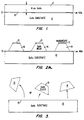
- Figs. 1-17 are, for example, in context to fabricating and assembling a shaped gallium arsenide block onto a silicon substrate for illustrative purposes only.
- Figs. 18-21 are, as further examples, in context to fabricating and assembling shaped silicon blocks onto a silicon substrate for illustrative purposes only.
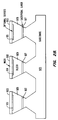
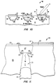
- trapezoidal shaped blocks self-align into inverted trapezoidal shaped recessed regions located on the top surface of the silicon wafer.
- Steps for such method include forming the gallium arsenide blocks, transferring the blocks into a solution forming a slurry, and spreading the slurry evenly over the top surface of a silicon substrate having recessed regions.
- the blocks self-align and settle into the recessed regions while being transported with the fluid across the top surface.
- the slurry is spread evenly over the top surface of a silicon substrate by way of mechanical means such as a brush, a scraper, tweezers, a pick, a doctor blade, and others.
- the mechanical means may be used to move or distribute the slurry and also to remove excess slurry.
- the method includes circulating the slurry over the top surface of the substrate having recessed regions. During the circulating step, the blocks self-align and settle into the recessed regions while being transported with the fluid across the top surface. The blocks which do not settle into recessed regions are then recirculated until a certain fill-factor is achieved.
- the mechanical means may also be used in conjunction with the circulating step. The details of fabricating the silicon substrate having recessed regions will be discussed in detail below after a brief discussion of forming the gallium arsenide blocks. Details of the method using the circulating step and related apparatus will be discussed in detail below after a discussion of fabricating the silicon substrate having recessed regions.
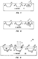
- the method provides as an example a step of forming trapezoidal shaped blocks from a gallium arsenide wafer. It should be noted that the shaped blocks are also micromachined structures or the like. Such step includes providing a gallium arsenide wafer 10 as illustrated in Fig. 1.
- the method also provides forming sacrificial layer 13 by chemical vapor deposition, sputtering, or the like overlying top surface 15 of gallium arsenide wafer 10.
- Such sacrificial layer 13 includes, for example, aluminum arsenide.
- Other sacrificial layers may include indium phosphate, silicon dioxide, photoresist, among other materials capable of being selectively etched.
- the sacrificial layer used depends upon the particular application.
- thickness for such layer is between about 0.1 ⁇ m and about 5.0 ⁇ m, and preferably at about 1 ⁇ m.
- a step of etching top surface 15 by methods such as wet etching, plasma etching, or reactive ion etching clears off any native oxide.
- a step of desorption in the presence of arsenic removes the native oxide layer.
- a subsequent step of preferential etching removes sacrificial layer 13 to facilitate the lift-off of each gallium arsenide block (also called a mesa shaped or trapezoidal shaped or truncated pyramid shaped structure) formed overlying sacrificial layer 13.
- gallium arsenide layer 17 forms overlying sacrificial layer 13.
- Such gallium arsenide layer may be fabricated by methods including molecular beam epitaxy, chemical vapor deposition, and others.
- the thickness (T) of the gallium arsenide layer is at least about 10 nm and greater, and preferably at about 10 ⁇ m and greater, depending upon the particular application.
- Fig. 2a illustrates gallium arsenide substrate 10 after such masking and etching steps and includes gallium arsenide blocks 19 and a photoresist layer 21 overlying gallium arsenide layer 17 (not shown).
- gallium arsenide layer 17 is etched up to sacrificial layer 13 as illustrated in Fig. 2a.
- Such etching step provides a plurality of shaped gallium arsenide blocks 19.
- the shaped blocks include a trapezoidal profile or truncated pyramid shape.
- Such trapezoidal profile may be fabricated by methods of wet etching, plasma etching, ion milling, reactive ion etching, among others, depending on the application.
- a wet etch produces a sloping profile along the sides or edges of each gallium arsenide block.
- a wet etch produces an outward sloping profile as illustrated in Fig. 2a.
- mask edges parallel to the [110] direction produces an inward sloping (or reverse mesa) profile.
- the outward sloping profile provides a desired shape which integrates into a silicon substrate having recessed regions shaped in a complementary manner.
- Ion milling produces gallium arsenide blocks with outward sloping profiles, depending upon the beam angle.
- Beam angle is adjusted between about 0° to about 30° from a normal to top surface 15 on gallium arsenide substrate 10.
- the entire structure is typically rotated during such etching step.
- Reactive ion etching also produces blocks having a shaped profile in many materials such as gallium arsenide, silicon, or others.
- a vertical etch may be used at a tilt to cut each sidewall angle.
- a substantially vertical etch process may also be tuned to undercut at a selected angle without tilting the substrate.
- a vertical etch or a reactive ion etch may be used in combination with a wet chemical etch to provide the undercut.
- Such etching methods create blocks having undercut sides or a reverse mesa profile, as shown in Fig. 2b.
- Fig. 2b illustrates reverse trapezoidal shaped blocks.
- substrate 925 (of material such as gallium arsenide, silicon, or the like) after such masking and etching steps and includes shaped blocks 929 on a sacrificial layer 927.
- a mask layer 933 overlies a device layer 931 which includes electronic or other devices or portions of devices.
- unexposed portions of block layer 929 are etched through sacrificial layer 927 as illustrated in Fig. 2b.
- such etching method may create blocks having substantially consistent shapes and/or profiles. Vertical etches and wet etches may be used or combined to produce such reverse mesa profiles.
- a plurality of shaped blocks 929 are thereby produced by removal of the sacrificial layer 927.
- Removal of the sacrificial layer 927 may be accomplished for example by selective etching, chemical conversion (such as preferentially oxidizing the sacrificial layer, preferentially converting the sacricial layer into porous Silicon, or others) followed by selective etching, thermal or ultrasonic or mechanical fracture, or dissolving, among others, and preferably by selective etching.
- the functionality of the sacrificial layer 927 may be included in the substrate 925, separating the blocks 929 by removal or etching of substrate 925 in whole or in part.
- trapezoidal shaped blocks are removed through a lift-off technique from gallium arsenide substrate 10 by preferential etching sacrificial layer 13 as illustrated in Fig. 3.
- lift-off technique occurs by, for example, a preferential wet etch of the aluminum arsenide sacrificial layer.
- wet etching step is typically performed by a chemical such as a hydrofluoric acid solution or the like.
- the etchant used substantially etches the sacrificial layer but does not aggressively attack gallium arsenide blocks and/or substrates.
- the wet etchant solution After separating the gallium arsenide blocks from substrate 10, methods of diluting and decanting the wet etchant solution remove the blocks from the solution.
- the wet etchant is diluted and decanted using purified water, methanol, ethanol, or the like.
- a rinsing step occurs after the diluting and decanting step.
- the rinsing step relies on solutions such as acetone, methanol, ethanol, or any other inert solution having low corrosive properties.
- Such solution also provides a medium (or fluid) for creating a mixture having blocks suspended therein or generally a slurry.
- an alternative lift-off method creates intermediate structure 250 of Fig. 4 from the gallium arsenide structure of Fig. 2a.
- Such alternative lift-off method also promotes lift-off of the shaped blocks in applications where the devices are formed onto the backside of the blocks.
- the method includes spreading a filler or wax layer 253 preferably high temperature wax overlying the top surface of exposed portions of sacrificial layer 13 and gaps 255 between each block 19.
- One such wax includes a product by the name of TECH WAX made by TRANSENE Co., Inc.
- the method then includes inverting the gallium arsenide structure of Fig. 2a and attaching top surface 21 onto intermediate substrate 257.
- Such intermediate substrate is, for example, a silicon wafer or the like.
- intermediate substrate surface 261 undergoes steps of etching off any native oxide preferably with a wet etchant such as hydrofluoric acid, and treating the cleaned surface with an adhesion promotor such as hexamethyldisilazane also called HMDS.
- HMDS hexamethyldisilazane also called HMDS.
- backside 263 is lapped until about 50 ⁇ m remains on substrate 10. The remaining thickness of substrate 10 is then etched up to aluminum arsenide layer 13.
- An etchant such as ammonium hydroxide and hydrogen peroxide (6:200 NH 3 OH:H 2 O 2 ) preferentially etches the gallium arsenide substrate up to aluminum arsenide layer 13. Accordingly, the aluminum arsenide layer acts as an etch stop protecting gallium arsenide blocks 19. Removing aluminum arsenide layer 13 requires a step of wet etching using an etchant such as hydrofluoric acid. Such etchant typically removes aluminum arsenide layer 13 after a short dip in such solution. After the aluminum arsenide layer is completely removed, steps including masking, sputtering, and etching form metallized ring contacts 265 as illustrated in Fig. 5.
- Such metallized ring contacts were made by patterns formed from photoresist layer 267.
- the metallization for such contacts include materials such as gold, aluminum, among others.
- other processing steps such as etching, masking, implantation, diffusion, and the like may be performed on the blocks to create other profiles as well as active devices thereon.
- a solution such as trichloroethane (TCA) dissolves the filler or wax disposed between each block 19 and photoresist layer 21, and lifts off the gallium arsenide blocks 19 from intermediate substrate 257.
- TCA trichloroethane
- the gallium arsenide blocks are transferred to an inert solution such as acetone, methanol, ethanol, or any other solution having low corrosive characteristics.
- inert solution and blocks are often called a mixture or generally a slurry.
- the method provides as another example steps of forming trapezoidal shaped blocks from a silicon-type wafer as illustrated in Fig. 18.
- steps include providing a second substrate, such as a silicon wafer 700 defining a block layer 703 with a bottom surface 705 and an upper surface 707.
- silicon wafer 700 is a single-side-polished wafer having a dimension of about 2" to about 16" with a thickness of about 10 ⁇ m to about 2000 ⁇ m, and is preferably a two inch silicon wafer of about 235 ⁇ m thickness.
- Bottom surface 705 is the polished side of silicon wafer 700
- upper surface 707 is the unpolished, rough side.
- the method also includes forming a sacrificial layer 709 overlying upper surface 707 by a technique such as chemical vapor deposition, sputtering, molecular beam epitaxy, or the like.
- Sacrificial layer 709 is a layer made of silicon nitride (SiN x ), silicon dioxide SiO 2 , metals, or organics, with a thickness of about 100 ⁇ to about 100 ⁇ m, and is preferably a SiN x layer of about 0.4 ⁇ m thickness.
- SiN x silicon nitride
- SiO 2 silicon dioxide
- metals or organics
- masking and etching steps can be used to form out of block layer 703 the trapezoidal shaped blocks or truncated pyramid shapes.
- the trapezoidal shaped block or truncated pyramid shaped structure includes a base with four sides protruding therefrom to a larger top surface. Each side creates an angle between about 20° and about 90° from the top surface to a side, and preferably is about 55°.
- the block may have a length between about 1 ⁇ m and about 1 cm, and a width between about 1 ⁇ m and about 1 cm, and preferably has a length of about 1.0 mm and a width of about 1.2 mm.
- the larger face is on and in contact with sacrificial layer 709.
- a subsequent step of preferential etching removes sacrificial layer 709 to free each trapezoidal shaped block formed overlying sacrificial layer 709.
- the blocks are then transferred into a fluid to form a slurry containing the larger trapezoidal shaped blocks.
- the method provides as another example steps of forming trapezoidal shaped blocks from a silicon-on-insulator (SOI) wafer as illustrated in Fig. 19.
- steps include providing a second substrate such as a SOI wafer 800, that defines a silicon substrate 803 with an upper surface 805, a sacrificial layer 807 overlying upper surface 805, and a block layer 809 overlying sacrificial layer 807.
- Sacrificial layer 807 composed of SiO 2 is an insulator layer of SOI wafer 800 and block layer 809 composed of silicon is a silicon-on-insulator layer of SOI wafer 800.
- SOI wafer 800 has a silicon-on-insulator layer of a thickness of about 1 ⁇ m to about 2000 ⁇ m, and an insulator layer of thickness of about 100 ⁇ to about 1000 ⁇ m, and preferably has a silicon-on-insulator layer of about 35 ⁇ m thick silicon, and an insulator layer of about 0.4 ⁇ m thick SiO 2 .
- masking and etching steps can be used to form out of block layer 809 the trapezoidal shaped blocks on and in contact with sacrificial layer 807.
- the trapezoidal shaped block or truncated pyramid shaped structure includes a base with four sides protruding therefrom to a larger top surface. Each side creates an angle between about 20° and about 90° from the top surface to a side, and preferably is about 55°.
- the block may have a length between about 1 ⁇ m and about 2000 ⁇ m, and a width between about 1 ⁇ m and about 2000 ⁇ m, and preferably has a length of about 150 ⁇ m and a width of about 150 ⁇ m.
- the larger face of the smaller trapezoidal shaped blocks is in contact with sacrificial layer 807.
- a subsequent step of preferential etching removes sacrificial layer 807 to free each trapezoidal shaped block formed overlying sacrificial layer 807.
- trapezoidal shaped blocks can be removed from contact with the sacrificial layer by steps such as preferential etching, ion milling, or dissolving the sacrificial layer. The blocks are then transferred into a fluid to form a slurry.
- the slowest etching planes for silicon in the KOH:H 2 O etching solution used are the ⁇ 111 ⁇ planes, which can be considered etch stops forming the sloping sides of the shaped blocks.
- the respective mask used to define the blocks must be aligned to the appropriate crystal axis.
- a mask 850 was used to form the silicon trapezoidal blocks 855.
- Silicon trapezoidal shaped block 855 is formed at the intersection of the diagonal lines on mask 850, and the larger face 860 of silicon trapezoidal shaped block 855 is in contact with sacrificial layer (respectively 709 and 807, for the first and second preceding silicon examples).
- the width of the diagonal mask lines in Fig. 20 must be twice the thickness (t) of silicon block layer.
- etching is completed when silicon block layer 703 or 809 is etched entirely through, and simultaneously when the corners are precisely formed. Continuing etching beyond this point does not change the overall dimensions of the trapezoidal shaped block, but merely rounds the corners. Because of geometric considerations, the width of the top face of the shaped block must be at least 3 ⁇ 2 times the thickness of the silicon block layer. This limits the aspect ratio of the blocks fabricated by this technique. This mask pattern utilizes as high as 50% of the silicon area if there is no distance between block corners.
- the etched silicon wafer is placed in concentrated HF etch solution to remove the shaped blocks from contact with the SiN x sacrificial layer and any remaining SiN x from the mask layer.
- the etched SOI wafer similarly is placed in concentrated HF etch solution to remove the shaped blocks from contact with the SiO 2 sacrificial layer and any remaining SiN x from the mask layer.
- This HF etch solution preferentially etches the SiO 2 and the SiNx to free the shaped blocks without etching the silicon shaped blocks.
- a HF solution having a concentration of about 1:1 HF:H 2 O was used to etch the sacrificial layer and residual SiNx to free the shaped blocks.
- the slurry comprises an inert solution (of fluid) and shaped blocks. Enough solution exists in the slurry to allow the blocks to slide across the top surface of the substrate.
- the amount of solution in the mixture is at least the same order as the amount of blocks. Of course, the amount of solution necessary depends upon characteristics such as block size, block material, substrate size, substrate material, and solution.
- the slurry is transferred or spread over top surface 53 of silicon substrate 50 as illustrated in Fig. 6. The details of the transferring technique are discussed below after a brief discussion in fabricating silicon substrate 50.
- silicon substrate 50 comprises etched recessed regions 55.
- a variety of techniques including wet etching, plasma etching, reactive ion etching, ion milling, among others provide recessed regions 50, or generally trenches, receptors, or binding sites. Such techniques etch recessed regions 50 with a geometric profile which is complementary to block 19.
- each recessed region includes a trapezoidal profile or inverted truncated pyramid shape. The trapezoidal profile allows block 19 to self-align and fit closely into recessed region 50 via the improved transferring technique.
- the transferring technique includes a step of evenly spreading or pouring the slurry over top surface 53.
- the transferring technique may be accomplished by pouring a vessel of slurry evenly over top surface 53.
- the slurry may also be transferred from a pipet, flask, beaker, or any other type of vessel and/or apparatus capable of evenly transferring the slurry over top surface 53.
- the slurry is poured over top surface 50 at a rate which allows substantial coverage of the top surface, but prevents blocks already disposed into the recessed regions from floating or popping out.
- Slurry flow is typically laminar but can be non-laminar, depending upon the particular application.
- the fluid flux over top surface 53 occurs at a velocity between about 0.01 mm/sec. and about 100 mm/sec. Preferably, fluid flux occurs at about 1 mm/sec.
- the blocks flow evenly with the fluid, tumble onto top surface 53, self-align, and settle into recessed regions 55.
- the transferring step may take place in a centrifuge or the like. A centrifuge, for example, places a force on the blocks already disposed in the recessed regions and thereby prevents such blocks from floating out with solution.
- the transferring technique may be accomplished by a method and related apparatus that includes circulating the slurry over top surface at a rate which allows blocks to dispose into the recessed regions.
- the rate may be adjusted to permit the blocks to fill the recessed regions so a desired fill-factor is achieved.
- the slurry is recirculated at a rate so that blocks which are not already disposed continuously flow across top surface until a certain fill-factor is attained.
- the slurry is recirculated at a rate which does not disturb blocks already disposed into recessed regions.
- the circulation rate is adjustable to accomodate a desired fill-factor, which will vary depending on the size of the blocks, number of recessed regions, and the specific application.
- Some applications require the integration of silicon circuits onto transparent substrates such as glass or plastic for use in an active matrix flat panel display. Each pixel or pixel element would have a small corresponding circuit assembled by the method. Larger circuits could also be assembled, such as for multichip modules which might require a number of different larger circuits on the same substrate. Each of these circuits could be etched to a specific shape and assembled by the method into matching recessed regions. Different applications can also require different fill-factors. For example, multichip modules could tolerate lower fill-factors than flat panel displays, because of the difference in number of components.
- the method and apparatus of the present invention exhibit high fill-factors for different sizes of shaped blocks. After the shaped blocks have been assembled onto the substrate, the disposed blocks can then be bonded and planarized, or the like, if necessary.
- an apparatus In order to continuously flow shaped blocks across the substrate, an apparatus circulates the slurry containing the shaped blocks across the substrate.
- the shaped blocks and fluid circulate within the apparatus and generally tumble onto the top surface of the substrate which is also contained in the apparatus.
- the shaped blocks self-align and engage with a recessed region having a complementary shape.
- the shaped blocks which are not disposed into recessed regions flow off the substrate and enter the recirculation path of the apparatus to flow over the substrate for disposition into recessed regions until a certain fill-factor is achieved.
- an apparatus 900 includes a vessel 903 and a pump 905.
- apparatus 900 was made entirely of glass but may be constructed of other suitable materials.
- Vessel 903 includes a receptacle 907 and a conduit 909.
- Vessel 903 contains a substrate 911 having recessed regions and the mixture of fluid and shaped blocks.
- Pump 905 is coupled to input 913 and dispenses a gas into conduit 909 to facilitate circulation of the fluid and shaped blocks over substrate 911 at a rate where at least one shaped block is disposed into a recessed region.
- Receptacle 907 includes a holder 919 and a funneled bottom 921.
- Holder 919 secures substrate 911 and is capable of moving substrate 911 to facilitate the filling of the recessed regions. Additionally, holder 919 agitates or orients substrate 911 so that shaped blocks not disposed in recessed regions can flow off substrate 911 and back into a recirculation path in vessel 903.
- the bottom of receptacle 907 is funneled to cause the shaped blocks not disposed into recessed regions on substrate 911 to fall to the bottom of receptacle 907 for recirculation through vessel 903. Shaped blocks not disposed into recessed regions then recirculate through vessel 903.
- funneled bottom 921 is coupled to input 913 of conduit 909.
- Shaped blocks not disposed into recessed regions tumble to funneled bottom 921 to input 913 of conduit 909, where pump 905 dispenses a gas, such as nitrogen.
- the injected gas forms bubbles within the fluid inside column 917 of conduit 909.
- a gas bubble transports a portion of the fluid and at least one shaped block funneled to input 913 through column 917 back to receptacle 907 through output 915 for attempted disposition into a recessed region.
- the gas bubble rises through column 917 and transports the fluid and the shaped block to output 915 leading back to receptacle 907.
- apparatus 900 uses nitrogen bubbles to circulate the fluid and the shaped blocks over substrate 911 without damaging the shaped blocks.
- apparatus 900 may use other media, or gases such as air, hydrogen (H 2 ), nitrogen (N 2 ), oxygen (O 2 ), or argon (Ar) which do not damage the blocks or otherwise react with the flu at which pump 905 dispenses the gas or transport medium can be changed to achieve different fill-factors of the recessed regions.
- the resulting structure 20 of the method described by Figs. 1-3 and 6 is illustrated in Fig. 7.
- the assembled microstructure includes silicon substrate 10, gallium arsenide blocks 19, and recessed regions 55.
- the trapezoidal shape of the blocks and recessed regions allows a block to self-align and fit closely into a recessed region during the transferring step.
- An angle (A) formed between one side of the block and the corresponding side of the recessed region is between about substantially 0° to about 20°. Preferably, such angle is less than about 5° but greater than substantially 0°. Such angle facilitates the self-alignment process of each block.
- the improved method allows for the fabrication of multiple blocks or microstructures onto a substrate by various shaped blocks and recessed region geometries and the fluid transferring step.
- the blocks 19 are attached into recessed regions 55 through eutectic layer 75 as represented in structure 70 of Fig. 8.
- a metallized layer such as gold, silver, solder, or the like is formed onto surface 73.
- the layer attaching the block with each recessed region may be a synthetic adhesive or the like instead of a eutectic layer. Process steps comprising masking, etching, and sputtering typically form such metallized layer.
- heating structure 70 forms eutectic layer 75 between metallization layer 73 and silicon substrate 10.
- the eutectic layer provides both mechanical and electrical contact between substrate 10 and block 19.
- the method of attaching the blocks onto the substrate provides an efficient, cost effective, and easy technique.
- the portions of the improved method of Figs. 1, 2, 4, 5, and 6 provides the resulting gallium arsenide light emitting diodes (LED) 200 as illustrated in Fig. 9.
- the gallium arsenide LED includes silicon substrate 203 and gallium arsenide block 205.
- Each gallium arsenide block includes at least metallized ring contacts 207, p-type gallium arsenide layer 209, n-type gallium arsenide layer 211, and eutectic layer 213.
- voltage is applied to metallized ring contact 207 or metallization layer. Photons (h ⁇ ) are illuminated from a center region within each metallized ring contact 207 of gallium arsenide block 205 as shown.
- the improved structure forms gallium arsenide light emitting diodes (LED) 90 as depicted in Fig. 10.
- the gallium arsenide LED includes silicon substrate 93 and gallium arsenide block 95.
- Each gallium arsenide block also includes at least metallized surface 97, p-type gallium arsenide layer 101, n-type gallium arsenide layer 103, and eutectic layer 105, similar to the preceding embodiment.
- voltage is applied to metallization layer 97 by, for example, a probe. Photons (h ⁇ ) are illuminated from an edge region instead of a center region of gallium arsenide block 95 as shown.
- the improved structure forms gallium arsenide structure 120 having tapered aperture opening 123 as illustrated in Fig. 11 (not to scale).
- a process step such as wet etching, ion milling, reactive ion etching, and others forms the tapered aperture opening 123.
- the gallium arsenide structure may be an LED, laser, or the like.
- gallium arsenide structure 120 includes substrate 125 and gallium arsenide block 127.
- Structure 120 also includes a top metallization layer 131 such as aluminum overlying gallium arsenide block 127 and an insulating layer 133.
- a ring contact layer 135 provides mechanical and electrical contact between substrate 125 and gallium arsenide block 127.
- a gallium arsenide block 137 Mechanical support and electrical contact for the gallium arsenide block comes from ledge 137. Also shown is a light emitting (or lasing) aperture 139 having a dimension between about 5 ⁇ m and about 40 ⁇ m. To turn-on the device, voltage is applied to metallization layer 131. Photons (h ⁇ ) illuminate from gallium arsenide block 127, through light emitting aperture 139, and through tapered aperture opening 123 as shown. Fiber optic cable 141 receives the photons.
- the improved method and resulting structure are in context to a trapezoidal shaped block made of gallium arsenide or silicon merely for illustrative purposes only.
- the improved method and structure can be in context to almost any block having shaped features.
- Shaped features allow such blocks to move over the surface of the substrate via fluid transport, align with a corresponding recessed region, and insert into such recessed region.
- Fig. 12 illustrates further examples of the shaped blocks.
- the blocks may, for example, include a rectangular shape 300, octagonal shape 303, or circular shape 305.
- the rectangular shaped block includes up to four orientations for insertion into a substrate having a corresponding recessed region.
- the octagonal shaped block includes up to eight orientations and the circular shaped block includes continuous orientations as long as the narrow end inserts first into the recessed region.
- Such blocks may also comprise a material such as silicon, gallium arsenide, aluminum gallium arsenide, diamond, germanium, other group III-V and II-VI compounds, multilayered structures, among others.
- Such multilayered structures may include metals, insulators such as silicon dioxide, silicon nitride and the like, and combinations thereof.
- the block can be made of almost any type of material capable of forming shaped features.
- such blocks are fabricated by methods including ion milling, reactive ion etching, and the like.
- an angle between a side of the block and the corresponding side of the recessed region for a disposed block is between about substantially 0° to about 20°. Preferably, such angle is less than about 5° but greater than substantially 0°.
- the shaped block assembles with a substrate such as a silicon wafer, plastic sheet, gallium arsenide wafer, glass substrate, ceramic substrate, or the like.
- the substrate includes almost any type of material capable of forming shaped recessed regions or generally binding sites or receptors thereon which complement the shaped blocks.
- a gallium arsenide block in the form of a diode was assembled onto a silicon substrate and operated.
- a slurry including gallium arsenide blocks were transferred such that the blocks self-aligned into recessed regions located on a top surface of a silicon substrate.
- the steps for such method included forming the gallium arsenide blocks, transferring the blocks into a solution forming a slurry, and transporting the slurry evenly over a top surface of a silicon substrate having recessed regions.
- the shaped blocks generally tumble onto the top surface of the substrate, self-align and engage with a recessed region having a complementary shape.
- a solution of ethylenediamine pyrocatechol pyrazine (EDP) or potassium hydroxide (KOH) produced recessed regions having a trapezoidal profile or inverted truncated pyramid shape.
- EDP ethylenediamine pyrocatechol pyrazine
- KOH potassium hydroxide
- Trapezoidal profiles occurred due to the selectivity (1:100) between the ⁇ 111 ⁇ plane and the ⁇ 100 ⁇ or ⁇ 110 ⁇ plane.
- the ⁇ 111 ⁇ plane etched slower than the ⁇ 100 ⁇ or ⁇ 110 ⁇ plane by a ratio of 1:100.
- an EDP solution etched recessed regions into a silicon substrate.
- EDP includes ethylenediamine (about 500 ml.), pyrocatechol (about 160 gms.), water (about 160 gms.), pyrazine (about 1 gm.).
- the EDP bath was also at a temperature of about 115 °C.
- a thermal oxide (SiO 2 ) layer having a thickness of about 200 nm was first formed on a top surface of such substrate. Masking and etching such oxide layer formed rectangular shaped regions. Such regions were then etched vertically about 10 ⁇ m forming square openings on the top surface about 23 ⁇ m in length. Sides protrude down symmetrically from each opening to a square base having a length of about 9 ⁇ m.
- an epi-ready two inch n-type gallium arsenide wafer provided a substrate for the formation of the self-aligning blocks.
- Native oxide on the top surface of such block was first cleared off by a desorption process.
- the desorption process included exposing the wafer to a temperature of about 700 °C and elements including arsenic.
- a sacrificial layer comprising 1 ⁇ m of doped or undoped aluminum arsenide was grown on and in contact with the top surface.
- a thickness of about 10.7 ⁇ m of silicon doped gallium arsenide was then grown through an MBE process overlying the aluminum arsenide layer. Silicon dopants were at a concentration of about 10 18 atoms/cm 3 .
- the top surface of the MBE grown layer was then patterned with photoresist.
- Patterning the top surface of the MBE grown layer included spreading a photoresist layer having a thickness of about 1.6 ⁇ m over the top surface of the MBE grown gallium arsenide layer.
- the photoresist used is a product made by Shipley under the name of AZ1400-31.
- Patterning steps also included at least exposing, developing, and baking the photoresist. Such baking step occurred at a temperature of about 120 °C for about 1 hour to hard-bake the photoresist layer.
- the patterning steps formed a plurality of rectangles each having a dimension of about 35 ⁇ m by 24 ⁇ m (exposed portions of the photoresist) on the top surface.
- wet etching the unexposed regions produced results which depended upon the orientation of the mask edges. If the mask edges were parallel to the [1 1 ⁇ 0] direction, wet etching the unexposed regions created outward sloping profiles from the top surface of each block. Alternatively, wet etching unexposed regions where mask edges were parallel to the [110] direction created inward sloping (or reverse mesa) profiles.
- gallium arsenide includes two distinct sets of ⁇ 111 ⁇ planes.
- each gallium atom on the surface has three arsenide atoms bonded below.
- each arsenide atom on the surface includes three gallium atoms bonded below.
- Each arsenide atom in the ⁇ 111 ⁇ B layer includes a pair of dangling electrons and is therefore exposed. Such dangling electrons are not present in the structure of the ⁇ 111 ⁇ A plane. Accordingly, ⁇ 111 ⁇ B planes tend to etch faster than ⁇ 111 ⁇ A planes, thereby forming blocks having a reverse mesa shape which is generally incompatible with the recessed regions etched on the silicon substrate.
- Mask edges parallel to the [110] plane produced more undercutting than the cases where mask edges were parallel to the [1 1 ⁇ 0] plane.
- mask edges parallel to the [110] direction produced about 1.1 ⁇ m of horizontal etching per micron of vertical etching near the tops of the blocks. Regions near the base of the blocks produced etches of about 0.4 ⁇ m of horizontal etching per micron of vertical etching.
- mask edges parallel to the [1 1 ⁇ 0] plane produced etches of about 0.8 ⁇ m of horizontal etching per micron of vertical etching for regions near the top of the blocks, and 0.1 ⁇ m of horizontal etching per micron of vertical etch near the bottom of the blocks.
- the formation of a square region at the base required a longer mask in the [110] direction.
- etchant concentration also affected the shape of each gallium arsenide block.
- a solution of phosphoric acid, hydrogen peroxide, and water (H 2 PO 3 :H 2 O 2 :H 2 O) provided a promising etchant for the MBE grown gallium arsenide layer in the present example.
- Such etchant created three distinct profiles, depending upon the amount of hydrogen peroxide and water added to phosphoric acid.
- Dilute concentrations of phosphoric acid (1:1:40 H 2 PO 3 :H 2 O 2 :H 2 O) created a trapezoidal or mesa shaped profile having a 30° angle between the top surface of the block and a corresponding side.
- Etchant solutions which were less concentrated produced shallower trapezoidal or mesa shaped profiles at angles from about 10° to 20°. Such shallower profiles were probably a result of etching reactions being transport limited in the ⁇ 111 ⁇ B planes.
- phosphoric acid (1:1:20 H 2 PO 3 :H 2 O 2 :H 2 O and above) created inward sloping (or reverse mesa) profiles limited by the reaction of the ⁇ 111 ⁇ B planes.
- a phosphoric acid concentration (1:1:30 H 2 PO 4 :H 2 O 2 :H 2 O) between the dilute and concentrated solutions provides better profiles for assembly with recessed regions etched on the silicon substrate.
- Such etchant produced blocks having angles of 55° parallel to the [110] plane and 49° parallel to the [1 1 ⁇ 0] plane, and typically etched the MBE grown layer at a rate of about 0.133 ⁇ m/minute (or about 133 nm/min). In producing the results described, etchant solution was typically replenished when depleted.
- a similar wet etchant (1:1:30 H 2 PO 3 :H 2 O 2 :H 2 O) facilitated the formation of aluminum gallium arsenide blocks from an aluminum gallium arsenide MBE grown layer.
- the presence of aluminum arsenide increased etching of the ⁇ 111 ⁇ B plane into the reaction-rate limited regime.
- ion milling was also used to create the gallium arsenide trapezoidal shaped blocks.
- Ion milling the MBE grown gallium arsenide layer provided outward sloping profiles ranging at angles of about 68° to 90° between the top surface and a corresponding side. To produce such angles, the ion beam angles ranged from about 0° to 25° in reference to a normal from the top surface of the MBE grown layer. Steeper beam angles (closer to 90°) generally created vertical or substantially vertical profiles. Ion milling also required the substrate to be rotated about a center axis during such processing step.
- processing variables included an argon gas etchant, pressure of about 50 millitorr, ion energy of about 1000 v, and an ion milling rate of 1 ⁇ m every seven minutes.
- argon gas etchant pressure of about 50 millitorr
- ion energy of about 1000 v
- ion milling rate 1 ⁇ m every seven minutes.
- the photoresist mask eroded laterally about 5 ⁇ m every 70 minutes during milling, sidewalls having angles at about 68° were produced.
- Selectivity between the gallium arsenide and photoresist was about 3:1. Ion milling produced substantially consistent gallium arsenide blocks and was therefore more effective than wet etching in this particular example.
- a final bath having a concentration of 1:1:30 H 2 PO 3 :H 2 O 2 :H 2 O was used to clear off remaining oxides of either gallium arsenide and aluminum arsenide. Such oxides were typically formed when aluminum arsenide was exposed to etching baths or ion milling. Hydrofluoric acid may then be used to clear off the oxide layers (typically rough looking and brown in appearance). Generally, such oxide layers reduce the effectiveness of hydrofluoric acid (HF) etching on the sacrificial aluminum arsenide layer.
- HF hydrofluoric acid
- a HF solution preferentially etched the sacrificial layer of aluminum arsenide to lift-off the gallium arsenide blocks.
- a HF solution having a concentration of about 5:1 H 2 O:HF was used to etch the sacrificial layer and lift off the blocks. Any blocks still remaining on the substrate possibly through surface tension can be mechanically removed from the substrate into a solution. Removed blocks include a base dimension of about 22 ⁇ m by 23 ⁇ m, compared to a designed dimension of 24 ⁇ m by 24 ⁇ m.
- a teflon pipet was used to remove a substantial portion of the HF solution from the gallium arsenide blocks. Any remaining HF was rinsed off with water. Such rinsing step created a mixture including blocks and water. An inert solution such as acetone then replaced the water to decrease any oxide formation on the blocks. Once in the inert solution, the blocks may cluster together and either float to the surface or settle to the bottom of the solution. Such clusters, often visible to the naked eye, decreased the effectiveness of a subsequent transferring step, and were therefore separated by mechanically agitating the solution with ultrasonic vibration.
- the inert solution including gallium arsenide blocks was then transferred (or poured) evenly over the top surface of the silicon substrate.
- a pipet was used to transfer such solution over the top surface of the substrate.
- the solution is transferred at a rate creating substantially a laminar flow.
- Such laminar flow allowed the blocks to tumble and/or slide onto the top surface of the substrate and then self-align into the recessed regions via the trapezoidal profile.
- the transfer rate should provide an even flow of solution including blocks over the substrate surface but should not free or remove any blocks already disposed into the recessed regions.
- Blocks fabricated by ion milling produced higher yields than wet etched blocks.
- Ion milled blocks having substantially consistent profiles self aligned and inserted into more than 90% of the recessed regions located on the substrate surface before the solution substantially evaporated. As the solution evaporates, surface tension often pulled a portion of the blocks out of the recessed regions. About 30% to 70% of the recessed regions remained filled after evaporation. The decrease in yield can be addressed by using liquids having lower surface tension during evaporation or by super critical drying methods which substantially eliminates surface, tension.
- blocks may be bonded into the recessed regions prior to evaporation of the solution, thereby fixing the yield.
- Photographs shown in Fig. 13 illustrate gallium arsenide blocks disposed into recessed regions of the silicon substrate 150 according to the present example.
- a top portion 153 of each recessed region is square and measures about 23 ⁇ m at length.
- the photograph includes recessed regions 155, silicon substrate 157, and trapezoidal shaped block 159.
- an illuminated diode 170 is shown in the photograph of Fig. 14.
- the photograph includes silicon substrate 173 and illuminated gallium arsenide LED 175.
- the gallium arsenide LED emitted infrared radiation while under electrical bias.
- Each gallium arsenide LED which was grown on an MBE layer included an N+ gallium arsenide cap layer (about 100 nm thickness), an N+ Al 0.1 Ga 0.9 As transport layer (about 1 ⁇ m thickness), a P- active region (about 1 ⁇ m thickness), and a P+ buffer layer (about 1 ⁇ m thickness).
- the gallium arsenide LED also required a ring metallized contact 400 for applying voltage and an opening 403 for light output at a top portion of each block as illustrated in Fig. 15.
- a current-voltage (I-V) curve 500 illustrated in Fig. 16 exhibits typical p-n junction characteristics for the gallium arsenide structure of Fig. 14.
- RTD's Gallium arsenide/aluminum arsenide resonant-tunneling diodes
- RTD's grown on an MBE layer include gallium arsenide wells (depth at about 5.0 nm) between two aluminum arsenide barriers (depth at about 2.5 nm).
- Oscillations (rf) observed after biasing the RTD's in the NDR region were limited to about 100 MHz. External capacitances and inductances of the biasing circuit caused such limitations in frequency.
- gallium arsenide block onto a silicon substrate for illustrative purposes only.
- the invention may be applied to forming gallium arsenide diodes onto silicon substrates.
- Another commercial application includes gallium arsenide lasers assembled with silicon integrated circuits. The silicon chips can communicate with other chips with integrated optical detectors on extremely high bit-rate optical channels.
- Other applications may also include integration of microwave gallium arsenide devices onto silicon integrated circuits for the purpose of microwave electronics.
- Still a further application includes microstructures integral with a plastic sheet forming active liquid crystal displays (ALCD) and the like. In such application, the plastic sheet may be fabricated by a technique including stamping, injection molding, among others.
- ACD active liquid crystal displays
- Advantages of the invention include for example the applicability of conventional metallization or other processes over the planar surface for interconnection of the integrated electronic devices or portions of electronic devices between the blocks and/or between blocks and other electronic devices on the substrate.
- the concept of the invention can be used with almost any type of microstructure which assembles onto a larger substrate.
- larger trapezoidal blocks were designed to have two-fold rotational symmetry with the size of the larger face having a dimension of about 1.0 mm x 1.2 mm and a depth of about 235 ⁇ m, and recessed regions were designed to correspond to the dimensions of the larger trapezoidal blocks.
- smaller trapezoidal blocks were designed to have four-fold symmetry with the size of the larger face having a dimension of about 150 ⁇ m x 150 ⁇ m and a depth of about 35 ⁇ m, and recessed regions were designed to correspond to the dimensions of the smaller trapezoidal blocks.
- the method and apparatus exhibited high fill-factors.
- the mixture or slurry including silicon shaped blocks and an inert fluid are transported over a top surface of a silicon substrate having complementary recessed regions by use of an apparatus that circulates the slurry over the substrate.
- a solution of potassium hydroxide (KOH) produced recessed regions having a trapezoidal profile or inverted truncated pyramid shape.
- the solution created trapezoidal shaped profiles or inverted truncated pyramid shapes having a larger face with lateral dimensions at the top surface with sides sloping inward at about 55° from the top surface of the substrate.
- Trapezoidal profiles occurred due to the selectivity (1:200) between the ⁇ 111 ⁇ plane and the ⁇ 100 ⁇ plane. Specifically, the ⁇ 111 ⁇ plane etched slower than the ⁇ 100 ⁇ plane by the approximate ratio of 1:200.
- the KOH solution etched trapezoidal recessed regions into about 500 ⁇ m thick silicon wafers (5 cm x 5 cm in overall area) using a mask consisting of rectangular openings.
- the KOH etchant solution used in the examples was a 1:2 (by weight) KOH:H 2 O solution at about 80°C.
- a silicon nitride (SiN x ) mask layer was first formed on a top surface of such substrates.
- trapezoidal shaped recessed regions formed trapezoidal shaped recessed regions.
- the depth of the trapezoidal recessed region is determined by the length of time the silicon substrate is etched. If the silicon is etched the correct length of time, recessed regions can be made which are identical in shape and size to the blocks.
- the larger recessed regions in the substrate had lateral dimensions of about 1.0 mm x 1.2 mm at the top surface and a depth of about 235 ⁇ m after about 23 minutes of etching to complement the larger trapezoidal shaped blocks.
- the mask in this experiment consisted of 191 holes corresponding to recessed regions, arranged in various test patterns.
- the smaller recessed regions in another substrate had lateral dimensions of about 150 ⁇ m x 150 ⁇ m at the top surface and a depth of about 35 ⁇ m after about 30 minutes of etching to complement the smaller trapezoidal shaped blocks.
- the mask in this experiment was simply an array of 64 x 64 holes (corresponding to 4,096 recessed regions) with about a 300 ⁇ m spacing between consecutive holes.
- the silicon nitride mask layer was not removed from the substrates and remained on the substrates throughout the microstructure assembling method.
- a single-side-polished two inch silicon wafer of about 235 ⁇ m thickness provided a substrate for the formation of self-aligning shaped blocks.
- the silicon wafer itself is the block layer from which the trapezoidal shaped blocks are formed.
- a SiN x layer of thickness about 0.4 ⁇ m was deposited on both the polished bottom surface of the wafer and the unpolished upper surface of the wafer.
- the SiN x layer overlying the unpolished upper surface of the wafer forms a sacrificial layer, and the SiN x layer overlying the polished bottom surface of the wafer forms a mask layer.
- the SiN x mask layer overlying the polished bottom surface of the wafer was then patterned with photoresist.
- Patterning the SiN x mask layer overlying the polished bottom surface of the wafer included spreading a photoresist layer over this SiN x layer.
- Patterning steps also included at least exposing, developing, and baking the photoresist. Such baking step occurred at a temperature of about 120°C for about 20 minutes to hard-bake the photoresist layer.
- the patterning steps formed a plurality of squares (or rectangles). After patterning, exposed regions were etched forming trapezoidal shaped blocks attached to the SiN x sacrificial layer.
- a SOI wafer provided a substrate for the formation of self-aligning shaped blocks.
- the particular SOI wafer used had a SOI layer of about 35 ⁇ m thickness with a silicon dioxide (SiO 2 ) layer of about 0.4 ⁇ m thickness separating it from the rest of the wafer.
- the 35 ⁇ m SOI layer is the block layer of silicon from which the trapezoidal shaped blocks are formed.
- the SiO 2 layer of about 0.4 ⁇ m thickness is the sacrificial layer.
- a SiN x mask layer of thickness about 0.4 ⁇ m was deposited on both 35 ⁇ m silicon block layer and patterned with photoresist.
- Patterning the SiN x mask layer overlying the upper surface of the wafer included spreading a photoresist layer over this SiN x mask layer. Patterning steps also included at least exposing, developing, and baking the photoresist. The patterning steps formed a plurality of rectangles each having a dimension of about 150 ⁇ m x 150 ⁇ m (exposed portions of the photoresist). After patterning, unexposed regions were etched forming trapezoidal shaped blocks attached to the SiO 2 sacrificial layer.
- the slowest etching planes for silicon in this KOH:H 2 O etching solution are the ⁇ 111 ⁇ planes, which can be considered etch stops forming the sloping sides of the shaped blocks.
- the respective mask used to define the blocks must be aligned to the appropriate crystal axis.
- a mask was used to form silicon trapezoidal shaped blocks. Trapezoidal shaped block is formed at the intersection of the diagonal lines on the mask. The width of the diagonal lines in the figure must be twice the thickness of the silicon block layer.
- Etching is completed when this silicon block layer is etched entirely through, and simultaneously when the corners are precisely formed. Continuing etching beyond this point does not change the overall dimensions of the trapezoidal shaped block, but merely rounds the corners. Because of geometric considerations, the width of the top face of the shaped block must be at least 3 ⁇ 2 times the thickness of the silicon block layer. This limits the aspect ratio of the blocks fabricated by this technique. This mask pattern utilizes as high as 50% of the silicon area if there is no distance between block corners.
- the etched silicon wafer is placed in concentrated HF etch solution to remove the shaped blocks from contact with the SiN x sacrificial layer and any remaining SiN x from the mask layer.
- the etched SOI wafer similarly is placed in concentrated HF etch solution to remove the shaped blocks from contact with the SiO 2 sacrificial layer and any remaining SiN x from the mask layer.
- This HF etch solution preferentially etches the SiO 2 and the SiN x to free the shaped blocks without etching the silicon shaped blocks.
- a HF solution having a concentration of about 1:1 HF:H 2 O was used to etch the sacrificial layer and residual SiN x to free the shaped blocks.
- the HF was decanted and water was added.
- water and the larger shaped blocks formed the mixture or slurry.
- methanol and the smaller shaped blocks formed the mixture or slurry.
- silicon is hydrophobic in nature, smaller shaped blocks having smaller mass tended to float on the surface of the water. The larger blocks did not have this problem because of their larger mass. Since methanol has both polar and nonpolar properties, the smaller shaped blocks did not float but preferably submerged into the fluid.
- the selection of the fluid used in the slurry may depend on the mass of the shaped block, among other factors.
- the mixture including approximately 500 of the larger shaped blocks and water (about 0.5 liter) was placed into the apparatus (about 4" diameter).
- the substrate was about 5 cm x 5 cm and contained 191 recessed regions in various patterns. Initially, small bubbles tended to stick to the larger shaped blocks and to the recessed regions on the substrate, due to the fact that all the silicon surfaces are hydrophobic. Adding a small amount of surfactant of about 5 drops to the water (1:100,000) made the silicon surfaces less hydrophobic and bubbles no longer stuck to the shaped blocks or to the recessed regions.
- the substrate was oriented at an angle which caused the incorrectly oriented blocks to slide off. Agitation and correct orientation of the substrate increased the rate at which the blocks filled the holes.
- the mixture including approximately 30,000 of the smaller shaped blocks and methanol (about 0.5 liter) was placed into the apparatus.
- the substrate was about 5 cm x 5 cm and contained a 3 cm x 3 cm array of 64 x 64 (4,096) recessed regions in the center of the substrate.
- Operating the apparatus in a manner similar to that used for the first silicon experiment with the larger shaped blocks resulted in a saturated fill-factor of about 70% after about 15 minutes.
- Roughening the top surface of the substrate having the recessed regions also leads to higher fill-factors.
- the substrate was lapped in about 0.5 ⁇ m Al 2 O 3 lapping powder just long enough (about 1-2 minutes) to create about a 0.3 ⁇ m roughness on the surface. Blocks in all orientations easily came off the substrate after it was roughened.
- saturated fill-factors of about 90% were achieved after about 15 minutes in the apparatus. After repeated runs of the second silicon experiment, it was determined that the 90% fill-factor achieved for the smaller blocks was a steady state condition.
- the block structure may also include a variety of shapes such as a cylindrical shape, rectangular shape, square shape, hexagonal shape, pyramid shape, T-shape, kidney shape, and others.
- the block structure includes widths, lengths, and heights to promote self-assembly for a desired orientation.
- more than one type of structure may be present in the mixture (solution and blocks) as long as each structure includes a specific binding site on the substrate.
Landscapes
- Engineering & Computer Science (AREA)
- Microelectronics & Electronic Packaging (AREA)
- Power Engineering (AREA)
- Computer Hardware Design (AREA)
- Physics & Mathematics (AREA)
- General Physics & Mathematics (AREA)
- Condensed Matter Physics & Semiconductors (AREA)
- Manufacturing & Machinery (AREA)
- Nonlinear Science (AREA)
- Chemical & Material Sciences (AREA)
- Mathematical Physics (AREA)
- Crystallography & Structural Chemistry (AREA)
- Ceramic Engineering (AREA)
- Optics & Photonics (AREA)
- Weting (AREA)
- Led Devices (AREA)
- Element Separation (AREA)
- Semiconductor Lasers (AREA)
- Recrystallisation Techniques (AREA)
- Light Receiving Elements (AREA)
- Micromachines (AREA)
- Optical Elements Other Than Lenses (AREA)
Applications Claiming Priority (2)
| Application Number | Priority Date | Filing Date | Title |
|---|---|---|---|
| US485478 | 1995-06-07 | ||
| US08/485,478 US5824186A (en) | 1993-12-17 | 1995-06-07 | Method and apparatus for fabricating self-assembling microstructures |
Publications (2)
| Publication Number | Publication Date |
|---|---|
| EP0747948A2 true EP0747948A2 (fr) | 1996-12-11 |
| EP0747948A3 EP0747948A3 (fr) | 2000-08-16 |
Family
ID=23928338
Family Applications (1)
| Application Number | Title | Priority Date | Filing Date |
|---|---|---|---|
| EP96109018A Withdrawn EP0747948A3 (fr) | 1995-06-07 | 1996-06-05 | Procédé et dispositif de fabrication de microstructures auto-assemblantes |
Country Status (6)
| Country | Link |
|---|---|
| US (1) | US5824186A (fr) |
| EP (1) | EP0747948A3 (fr) |
| JP (1) | JPH09120943A (fr) |
| CN (2) | CN1059290C (fr) |
| AU (1) | AU708552B2 (fr) |
| CA (1) | CA2177219A1 (fr) |
Cited By (31)
| Publication number | Priority date | Publication date | Assignee | Title |
|---|---|---|---|---|
| WO2000001014A1 (fr) * | 1998-06-29 | 2000-01-06 | Osram Opto Semiconductors Gmbh & Co. Ohg | Procede de production et de separation de diodes electroluminescentes a semi-conducteur microscopiques |
| WO2000046854A1 (fr) * | 1999-02-05 | 2000-08-10 | Alien Technology Corporation | Appareils et procedes de formation d'ensembles |
| WO2000049658A1 (fr) * | 1999-02-16 | 2000-08-24 | Alien Technology Corporation | De de circuit integre fonctionnellement symetrique |
| WO2000055916A1 (fr) * | 1999-03-16 | 2000-09-21 | Alien Technology Corporation | Procedes et appareil pour la fabrication d'un ensemble modulaire multiple |
| FR2817399A1 (fr) * | 2000-11-30 | 2002-05-31 | St Microelectronics Sa | Puce electronique multifonctions |
| US6731353B1 (en) | 2001-08-17 | 2004-05-04 | Alien Technology Corporation | Method and apparatus for transferring blocks |
| WO2004051701A2 (fr) * | 2002-11-29 | 2004-06-17 | Upm Rafsec Oy | Procede pour fixer des puces a un transpondeur |
| US6850312B2 (en) | 1999-03-16 | 2005-02-01 | Alien Technology Corporation | Apparatuses and methods for flexible displays |
| US6927085B2 (en) | 1999-02-05 | 2005-08-09 | Alien Technology Corporation | Web fabrication of devices |
| US6980184B1 (en) | 2000-09-27 | 2005-12-27 | Alien Technology Corporation | Display devices and integrated circuits |
| US7244326B2 (en) | 2003-05-16 | 2007-07-17 | Alien Technology Corporation | Transfer assembly for manufacturing electronic devices |
| US7727804B2 (en) | 1993-12-17 | 2010-06-01 | The Regents Of The University Of California | Method and apparatus for fabricating self-assembling microstructures |
| US8404525B2 (en) | 2006-01-10 | 2013-03-26 | Semiconductor Energy Laboratory Co., Ltd. | Semiconductor device, manufacturing method of semiconductor device, and RFID tag |
| EP2612380A2 (fr) * | 2010-09-01 | 2013-07-10 | Nthdegree Technologies Worldwide Inc. | Appareil électroluminescent, générateur d'énergie ou autre appareil électronique et son procédé de fabrication |
| EP2688093A1 (fr) * | 2012-07-19 | 2014-01-22 | Technische Universität Ilmenau | Procédé et appareil permettant l'auto-assemblage de composants sur un substrat |
| EP2617781A3 (fr) * | 2010-09-01 | 2014-03-19 | Nthdegree Technologies Worldwide Inc. | Diodes, compositions imprimables d'une suspension liquide ou en gel de diodes ou d'autres circuits intégrés à deux bornes et procédés de fabrication associés |
| WO2014040614A1 (fr) * | 2012-09-11 | 2014-03-20 | Osram Opto Semiconductors Gmbh | Dispositif optoélectronique et son procédé de production |
| US8809126B2 (en) | 2007-05-31 | 2014-08-19 | Nthdegree Technologies Worldwide Inc | Printable composition of a liquid or gel suspension of diodes |
| US8846457B2 (en) | 2007-05-31 | 2014-09-30 | Nthdegree Technologies Worldwide Inc | Printable composition of a liquid or gel suspension of diodes |
| US8852467B2 (en) | 2007-05-31 | 2014-10-07 | Nthdegree Technologies Worldwide Inc | Method of manufacturing a printable composition of a liquid or gel suspension of diodes |
| US8877101B2 (en) | 2007-05-31 | 2014-11-04 | Nthdegree Technologies Worldwide Inc | Method of manufacturing a light emitting, power generating or other electronic apparatus |
| WO2015036887A1 (fr) * | 2013-09-13 | 2015-03-19 | Koninklijke Philips N.V. | Boîtier à grille de connexions pour del à puce retournée |
| US9018833B2 (en) | 2007-05-31 | 2015-04-28 | Nthdegree Technologies Worldwide Inc | Apparatus with light emitting or absorbing diodes |
| US9105812B2 (en) | 2007-05-31 | 2015-08-11 | Nthdegree Technologies Worldwide Inc | Diode for a printable composition |
| US9130124B2 (en) | 2007-05-31 | 2015-09-08 | Nthdegree Technologies Worldwide Inc | Diode for a printable composition |
| US9236527B2 (en) | 2007-05-31 | 2016-01-12 | Nthdegree Technologies Worldwide Inc | Light emitting, photovoltaic or other electronic apparatus and system |
| US9343593B2 (en) | 2007-05-31 | 2016-05-17 | Nthdegree Technologies Worldwide Inc | Printable composition of a liquid or gel suspension of diodes |
| US9419179B2 (en) | 2007-05-31 | 2016-08-16 | Nthdegree Technologies Worldwide Inc | Diode for a printable composition |
| US9425357B2 (en) | 2007-05-31 | 2016-08-23 | Nthdegree Technologies Worldwide Inc. | Diode for a printable composition |
| US9534772B2 (en) | 2007-05-31 | 2017-01-03 | Nthdegree Technologies Worldwide Inc | Apparatus with light emitting diodes |
| EP4068346A1 (fr) * | 2021-03-31 | 2022-10-05 | Nederlandse Organisatie voor toegepast- natuurwetenschappelijk onderzoek TNO | Substrat composite |
Families Citing this family (195)
| Publication number | Priority date | Publication date | Assignee | Title |
|---|---|---|---|---|
| JP3097557B2 (ja) * | 1996-05-20 | 2000-10-10 | 日本電気株式会社 | 半導体装置の製造方法 |
| JP2002507765A (ja) | 1998-03-18 | 2002-03-12 | イー−インク コーポレイション | 電気泳動ディスプレイおよびそのディスプレイにアドレスするためのシステム |
| WO1999059101A2 (fr) | 1998-05-12 | 1999-11-18 | E-Ink Corporation | Support electrophoretique micro-encapsule a adressage electrostatique pour applications de systeme a dessiner |
| US6312304B1 (en) | 1998-12-15 | 2001-11-06 | E Ink Corporation | Assembly of microencapsulated electronic displays |
| US6281038B1 (en) * | 1999-02-05 | 2001-08-28 | Alien Technology Corporation | Methods for forming assemblies |
| US6468638B2 (en) | 1999-03-16 | 2002-10-22 | Alien Technology Corporation | Web process interconnect in electronic assemblies |
| US6531997B1 (en) | 1999-04-30 | 2003-03-11 | E Ink Corporation | Methods for addressing electrophoretic displays |
| US6504524B1 (en) | 2000-03-08 | 2003-01-07 | E Ink Corporation | Addressing methods for displays having zero time-average field |
| WO2001007961A1 (fr) | 1999-07-21 | 2001-02-01 | E Ink Corporation | Utilisation d'un condensateur de memorisation pour ameliorer la performance d'un affichage electronique matriciel actif |
| JP2001217245A (ja) * | 2000-02-04 | 2001-08-10 | Sharp Corp | 電子部品およびその製造方法 |
| JP2001217411A (ja) * | 2000-02-04 | 2001-08-10 | Sharp Corp | 電子部品およびその製造方法 |
| WO2001062517A1 (fr) * | 2000-02-22 | 2001-08-30 | Toray Engineering Company,Limited | Carte d'identification sans contact ou analogue et procede de fabrication correspondant |
| JP2001257218A (ja) * | 2000-03-10 | 2001-09-21 | Sony Corp | 微細チップの実装方法 |
| JP4360015B2 (ja) * | 2000-03-17 | 2009-11-11 | セイコーエプソン株式会社 | 有機el表示体の製造方法、半導体素子の配置方法、半導体装置の製造方法 |
| WO2001095375A1 (fr) | 2000-06-06 | 2001-12-13 | The Penn State Research Foundation | Procede d'assemblage electrofluidique destine a l'integration de dispositifs electroniques sur un substrat |
| US6730990B2 (en) | 2000-06-30 | 2004-05-04 | Seiko Epson Corporation | Mountable microstructure and optical transmission apparatus |
| US6723576B2 (en) | 2000-06-30 | 2004-04-20 | Seiko Epson Corporation | Disposing method for semiconductor elements |
| JP2002015866A (ja) * | 2000-06-30 | 2002-01-18 | Seiko Epson Corp | 有機el表示体の製造方法 |
| JP3829594B2 (ja) * | 2000-06-30 | 2006-10-04 | セイコーエプソン株式会社 | 素子実装方法と光伝送装置 |
| JP4239439B2 (ja) | 2000-07-06 | 2009-03-18 | セイコーエプソン株式会社 | 光学装置およびその製造方法ならびに光伝送装置 |
| US6605902B2 (en) | 2000-07-07 | 2003-08-12 | Seiko Epson Corporation | Display and electronic device |
| US6583580B2 (en) | 2000-07-07 | 2003-06-24 | Seiko Epson Corporation | EL element driving circuit and method, and electronic apparatus |
| JP3840926B2 (ja) * | 2000-07-07 | 2006-11-01 | セイコーエプソン株式会社 | 有機el表示体及びその製造方法、並びに電子機器 |
| JP3815269B2 (ja) | 2000-07-07 | 2006-08-30 | セイコーエプソン株式会社 | 有機el表示体及びその製造方法、孔開き基板、電気光学装置及びその製造方法、並びに電子機器 |
| JP3915868B2 (ja) * | 2000-07-07 | 2007-05-16 | セイコーエプソン株式会社 | 強誘電体メモリ装置およびその製造方法 |
| US6683333B2 (en) | 2000-07-14 | 2004-01-27 | E Ink Corporation | Fabrication of electronic circuit elements using unpatterned semiconductor layers |
| WO2002009175A2 (fr) * | 2000-07-20 | 2002-01-31 | President And Fellows Of Harvard College | Reseaux electriques auto-assembles |
| JP2002076436A (ja) * | 2000-08-29 | 2002-03-15 | Kyocera Corp | Ledアレイ |
| US6780696B1 (en) * | 2000-09-12 | 2004-08-24 | Alien Technology Corporation | Method and apparatus for self-assembly of functional blocks on a substrate facilitated by electrode pairs |
| JP4491948B2 (ja) | 2000-10-06 | 2010-06-30 | ソニー株式会社 | 素子実装方法および画像表示装置の製造方法 |
| DE10053334B4 (de) * | 2000-10-27 | 2018-08-02 | Robert Bosch Gmbh | Verfahren und Vorrichtung zur Steuerung eines Stellelements in einem Fahrzeug |
| US6448109B1 (en) * | 2000-11-15 | 2002-09-10 | Analog Devices, Inc. | Wafer level method of capping multiple MEMS elements |
| US20020149107A1 (en) * | 2001-02-02 | 2002-10-17 | Avery Dennison Corporation | Method of making a flexible substrate containing self-assembling microstructures |
| AU2002239287A1 (en) * | 2000-11-21 | 2002-06-03 | Avery Dennison Corporation | Display device and methods of manufacture and control |
| US7199527B2 (en) * | 2000-11-21 | 2007-04-03 | Alien Technology Corporation | Display device and methods of manufacturing and control |
| KR100361593B1 (ko) * | 2000-11-23 | 2002-11-22 | 주식회사일진 | 볼록 요철을 갖는 광학집적회로 소자, 그 제조방법, 그광학집적 회로 소자를 이용하여 제조한 광통신용 송수신장치의 모듈 |
| US6479315B1 (en) * | 2000-11-27 | 2002-11-12 | Microscan Systems, Inc. | Process for manufacturing micromechanical and microoptomechanical structures with single crystal silicon exposure step |
| US6794221B2 (en) * | 2000-11-29 | 2004-09-21 | Hrl Laboratories, Llc | Method of placing elements into receptors in a substrate |
| US6291266B1 (en) * | 2000-11-29 | 2001-09-18 | Hrl Laboratories, Llc | Method for fabricating large area flexible electronics |
| US6611237B2 (en) | 2000-11-30 | 2003-08-26 | The Regents Of The University Of California | Fluidic self-assembly of active antenna |
| US6951596B2 (en) | 2002-01-18 | 2005-10-04 | Avery Dennison Corporation | RFID label technique |
| JP2002359358A (ja) | 2001-03-26 | 2002-12-13 | Seiko Epson Corp | 強誘電体メモリ及び電子機器 |
| US6864435B2 (en) * | 2001-04-25 | 2005-03-08 | Alien Technology Corporation | Electrical contacts for flexible displays |
| JP4982926B2 (ja) * | 2001-05-17 | 2012-07-25 | ソニー株式会社 | 素子配列方法 |
| US6606247B2 (en) | 2001-05-31 | 2003-08-12 | Alien Technology Corporation | Multi-feature-size electronic structures |
| JP2003048200A (ja) * | 2001-08-06 | 2003-02-18 | Univ Waseda | マイクロマシンの製造方法 |
| US6861720B1 (en) * | 2001-08-29 | 2005-03-01 | Amkor Technology, Inc. | Placement template and method for placing optical dies |
| US7253091B2 (en) | 2001-09-28 | 2007-08-07 | Hrl Laboratories, Llc | Process for assembling three-dimensional systems on a chip and structure thus obtained |
| US7018575B2 (en) * | 2001-09-28 | 2006-03-28 | Hrl Laboratories, Llc | Method for assembly of complementary-shaped receptacle site and device microstructures |
| US6974604B2 (en) * | 2001-09-28 | 2005-12-13 | Hrl Laboratories, Llc | Method of self-latching for adhesion during self-assembly of electronic or optical components |
| US7351660B2 (en) * | 2001-09-28 | 2008-04-01 | Hrl Laboratories, Llc | Process for producing high performance interconnects |
| JP2003141761A (ja) * | 2001-10-31 | 2003-05-16 | Sanyo Electric Co Ltd | 光ディスク装置および記録/再生方法 |
| ATE432240T1 (de) * | 2001-11-09 | 2009-06-15 | Wispry Inc | Dreischichtige strahl-mems-einrichtung und diesbezügliche verfahren |
| US20040240034A1 (en) * | 2001-11-30 | 2004-12-02 | Scharf Bruce R. | Diffraction compensation using a patterned reflector |
| JP3844061B2 (ja) * | 2002-01-16 | 2006-11-08 | ソニー株式会社 | 電子部品の配置方法及びその装置 |
| JP4082031B2 (ja) * | 2002-01-17 | 2008-04-30 | ソニー株式会社 | 素子の配列方法、及び表示装置 |
| US7214569B2 (en) * | 2002-01-23 | 2007-05-08 | Alien Technology Corporation | Apparatus incorporating small-feature-size and large-feature-size components and method for making same |
| US6825049B2 (en) * | 2002-01-24 | 2004-11-30 | Massachusetts Institute Of Technology | Method and system for field assisted statistical assembly of wafers |
| US7080444B1 (en) * | 2002-02-28 | 2006-07-25 | Alien Technology Corporation | Apparatus for forming an electronic assembly |
| US7223672B2 (en) | 2002-04-24 | 2007-05-29 | E Ink Corporation | Processes for forming backplanes for electro-optic displays |
| JP3960874B2 (ja) * | 2002-07-31 | 2007-08-15 | シャープ株式会社 | コーナーキューブアレイおよびその製造方法 |
| US6867983B2 (en) * | 2002-08-07 | 2005-03-15 | Avery Dennison Corporation | Radio frequency identification device and method |
| JP4057861B2 (ja) * | 2002-08-20 | 2008-03-05 | 松下電器産業株式会社 | 半導体レーザ装置及びその製造方法 |
| JP2004119620A (ja) * | 2002-09-25 | 2004-04-15 | Matsushita Electric Ind Co Ltd | 半導体装置及びその製造方法 |
| JP4197420B2 (ja) | 2002-09-27 | 2008-12-17 | パナソニック株式会社 | 半導体装置の製造方法 |
| US7224280B2 (en) * | 2002-12-31 | 2007-05-29 | Avery Dennison Corporation | RFID device and method of forming |
| US6940408B2 (en) * | 2002-12-31 | 2005-09-06 | Avery Dennison Corporation | RFID device and method of forming |
| US7018867B2 (en) * | 2003-02-06 | 2006-03-28 | Intel Corporation | Fabricating stacked chips using fluidic templated-assembly |
| US7225992B2 (en) * | 2003-02-13 | 2007-06-05 | Avery Dennison Corporation | RFID device tester and method |
| US7253735B2 (en) | 2003-03-24 | 2007-08-07 | Alien Technology Corporation | RFID tags and processes for producing RFID tags |
| US7059518B2 (en) * | 2003-04-03 | 2006-06-13 | Avery Dennison Corporation | RFID device detection system and method |
| US7501984B2 (en) * | 2003-11-04 | 2009-03-10 | Avery Dennison Corporation | RFID tag using a surface insensitive antenna structure |
| US7652636B2 (en) * | 2003-04-10 | 2010-01-26 | Avery Dennison Corporation | RFID devices having self-compensating antennas and conductive shields |
| US7930815B2 (en) * | 2003-04-11 | 2011-04-26 | Avery Dennison Corporation | Conductive pattern and method of making |
| US20040200061A1 (en) * | 2003-04-11 | 2004-10-14 | Coleman James P. | Conductive pattern and method of making |
| JP3927919B2 (ja) * | 2003-05-07 | 2007-06-13 | 松下電器産業株式会社 | 半導体装置の製造方法 |
| US7223635B1 (en) | 2003-07-25 | 2007-05-29 | Hrl Laboratories, Llc | Oriented self-location of microstructures with alignment structures |
| JP4613489B2 (ja) * | 2003-12-08 | 2011-01-19 | ソニー株式会社 | 素子配列方法及び表示装置 |
| JP4396285B2 (ja) | 2004-01-21 | 2010-01-13 | ソニー株式会社 | 素子配列基板および素子配列方法 |
| JP3978189B2 (ja) | 2004-01-23 | 2007-09-19 | 松下電器産業株式会社 | 半導体装置の製造方法及びその製造装置 |
| US20080055581A1 (en) * | 2004-04-27 | 2008-03-06 | Rogers John A | Devices and methods for pattern generation by ink lithography |
| WO2005104756A2 (fr) * | 2004-04-27 | 2005-11-10 | The Board Of Trustees Of The University Of Illinois | Dispositifs de formation de motifs composites pour lithographie molle |
| JP2005342879A (ja) * | 2004-05-31 | 2005-12-15 | Noriya Hiruta | マイクロ部品の状態制御方法、及びそれらを含むアレイシステム装置 |
| US7943491B2 (en) | 2004-06-04 | 2011-05-17 | The Board Of Trustees Of The University Of Illinois | Pattern transfer printing by kinetic control of adhesion to an elastomeric stamp |
| US7799699B2 (en) * | 2004-06-04 | 2010-09-21 | The Board Of Trustees Of The University Of Illinois | Printable semiconductor structures and related methods of making and assembling |
| KR101746412B1 (ko) | 2004-06-04 | 2017-06-14 | 더 보오드 오브 트러스티스 오브 더 유니버시티 오브 일리노이즈 | 인쇄가능한 반도체소자들의 제조 및 조립방법과 장치 |
| US8217381B2 (en) | 2004-06-04 | 2012-07-10 | The Board Of Trustees Of The University Of Illinois | Controlled buckling structures in semiconductor interconnects and nanomembranes for stretchable electronics |
| US7521292B2 (en) | 2004-06-04 | 2009-04-21 | The Board Of Trustees Of The University Of Illinois | Stretchable form of single crystal silicon for high performance electronics on rubber substrates |
| US7307527B2 (en) * | 2004-07-01 | 2007-12-11 | Avery Dennison Corporation | RFID device preparation system and method |
| US20060044769A1 (en) * | 2004-09-01 | 2006-03-02 | Forster Ian J | RFID device with magnetic coupling |
| US7629026B2 (en) * | 2004-09-03 | 2009-12-08 | Eastman Kodak Company | Thermally controlled fluidic self-assembly |
| US20060051517A1 (en) * | 2004-09-03 | 2006-03-09 | Eastman Kodak Company | Thermally controlled fluidic self-assembly method and support |
| US7251882B2 (en) | 2004-09-03 | 2007-08-07 | Eastman Kodak Company | Method for assembling micro-components to binding sites |
| US7501955B2 (en) * | 2004-09-13 | 2009-03-10 | Avery Dennison Corporation | RFID device with content insensitivity and position insensitivity |
| US7500307B2 (en) | 2004-09-22 | 2009-03-10 | Avery Dennison Corporation | High-speed RFID circuit placement method |
| US7452748B1 (en) | 2004-11-08 | 2008-11-18 | Alien Technology Corporation | Strap assembly comprising functional block deposited therein and method of making same |
| US7551141B1 (en) | 2004-11-08 | 2009-06-23 | Alien Technology Corporation | RFID strap capacitively coupled and method of making same |
| US7353598B2 (en) * | 2004-11-08 | 2008-04-08 | Alien Technology Corporation | Assembly comprising functional devices and method of making same |
| JP4548096B2 (ja) * | 2004-11-11 | 2010-09-22 | ソニー株式会社 | 半導体チップと基板との嵌合構造、半導体チップ実装方法及び電子装置 |
| US7385284B2 (en) | 2004-11-22 | 2008-06-10 | Alien Technology Corporation | Transponder incorporated into an electronic device |
| US7688206B2 (en) | 2004-11-22 | 2010-03-30 | Alien Technology Corporation | Radio frequency identification (RFID) tag for an item having a conductive layer included or attached |
| US7332361B2 (en) * | 2004-12-14 | 2008-02-19 | Palo Alto Research Center Incorporated | Xerographic micro-assembler |
| US7687277B2 (en) | 2004-12-22 | 2010-03-30 | Eastman Kodak Company | Thermally controlled fluidic self-assembly |
| TW200633037A (en) * | 2005-01-24 | 2006-09-16 | Matsushita Electric Ind Co Ltd | Manufacturing method for semiconductor chips, and semiconductor chip |
| US7400490B2 (en) * | 2005-01-25 | 2008-07-15 | Naturalnano Research, Inc. | Ultracapacitors comprised of mineral microtubules |
| US7625780B2 (en) * | 2005-03-15 | 2009-12-01 | Regents Of The University Of Minnesota | Fluidic heterogeneous microsystems assembly and packaging |
| US7623034B2 (en) | 2005-04-25 | 2009-11-24 | Avery Dennison Corporation | High-speed RFID circuit placement method and device |
| US7542301B1 (en) | 2005-06-22 | 2009-06-02 | Alien Technology Corporation | Creating recessed regions in a substrate and assemblies having such recessed regions |
| US20070007237A1 (en) * | 2005-07-05 | 2007-01-11 | National Taiwan University | Method for self-assembling microstructures |
| US7943052B2 (en) * | 2005-07-05 | 2011-05-17 | National Taiwan University | Method for self-assembling microstructures |
| US20070031992A1 (en) * | 2005-08-05 | 2007-02-08 | Schatz Kenneth D | Apparatuses and methods facilitating functional block deposition |
| WO2007024764A1 (fr) * | 2005-08-22 | 2007-03-01 | Avery Dennison Corporation | Procede pour realiser des dispositifs rfid |
| US7555826B2 (en) * | 2005-12-22 | 2009-07-07 | Avery Dennison Corporation | Method of manufacturing RFID devices |
| US7154283B1 (en) | 2006-02-22 | 2006-12-26 | Avery Dennison Corporation | Method of determining performance of RFID devices |
| EP1991723A2 (fr) | 2006-03-03 | 2008-11-19 | The Board Of Trustees Of The University Of Illinois | Procede pour fabriquer des nanotubes ou des ensembles de nanotubes alignes dans l'espace |
| US7774929B2 (en) * | 2006-03-14 | 2010-08-17 | Regents Of The University Of Minnesota | Method of self-assembly on a surface |
| US20100186226A1 (en) * | 2006-06-23 | 2010-07-29 | University Of Washington, The | Fluidic self-assembly for system integration |
| US7875952B1 (en) | 2006-09-19 | 2011-01-25 | Hrl Laboratories, Llc | Method of transistor level heterogeneous integration and system |
| WO2008086090A1 (fr) * | 2007-01-05 | 2008-07-17 | University Of Washington | Système d'analyse optique intégré hétérogène auto-assemblé |
| KR101610885B1 (ko) | 2007-01-17 | 2016-04-08 | 더 보오드 오브 트러스티스 오브 더 유니버시티 오브 일리노이즈 | 프린팅기반 어셈블리에 의해 제조되는 광학 시스템 |
| US8579434B2 (en) | 2007-11-07 | 2013-11-12 | University Of Washington Through Its Center For Commercialization | Free-standing two-sided device fabrication |
| JP5140413B2 (ja) * | 2007-12-28 | 2013-02-06 | 株式会社日立製作所 | 実装基板、及びこの実装基板を備えるled光源装置 |
| US7874474B2 (en) * | 2008-01-22 | 2011-01-25 | University Of Washington | Self-assembly of elements using microfluidic traps |
| US7861405B2 (en) * | 2008-03-03 | 2011-01-04 | Palo Alto Research Center Incorporated | System for forming a micro-assembler |
| TWI500364B (zh) | 2008-03-05 | 2015-09-11 | 美國伊利諾大學理事會 | 可延展且可折疊的電子裝置 |
| US8470701B2 (en) | 2008-04-03 | 2013-06-25 | Advanced Diamond Technologies, Inc. | Printable, flexible and stretchable diamond for thermal management |
| US8946683B2 (en) * | 2008-06-16 | 2015-02-03 | The Board Of Trustees Of The University Of Illinois | Medium scale carbon nanotube thin film integrated circuits on flexible plastic substrates |
| US8389862B2 (en) | 2008-10-07 | 2013-03-05 | Mc10, Inc. | Extremely stretchable electronics |
| US8886334B2 (en) | 2008-10-07 | 2014-11-11 | Mc10, Inc. | Systems, methods, and devices using stretchable or flexible electronics for medical applications |
| US8372726B2 (en) | 2008-10-07 | 2013-02-12 | Mc10, Inc. | Methods and applications of non-planar imaging arrays |
| US8097926B2 (en) | 2008-10-07 | 2012-01-17 | Mc10, Inc. | Systems, methods, and devices having stretchable integrated circuitry for sensing and delivering therapy |
| WO2010042653A1 (fr) | 2008-10-07 | 2010-04-15 | Mc10, Inc. | Ballonnet de cathéter comportant un circuit intégré étirable et un réseau de détecteurs |
| KR20110125655A (ko) * | 2009-02-27 | 2011-11-21 | 알타 디바이씨즈, 인크. | 증착 및 액피텍셜 리프트 오프 공정을 통한 타일형 기판 |
| US8748730B2 (en) * | 2009-03-13 | 2014-06-10 | California Institute Of Technology | Systems and methods for concentrating solar energy without tracking the sun |
| EP2430652B1 (fr) | 2009-05-12 | 2019-11-20 | The Board of Trustees of the University of Illionis | Ensembles imprimés de diodes électroluminescentes inorganiques microscopiques ultraminces pour dispositifs d'affichage déformables et semi-transparents |
| US9723122B2 (en) | 2009-10-01 | 2017-08-01 | Mc10, Inc. | Protective cases with integrated electronics |
| US10441185B2 (en) | 2009-12-16 | 2019-10-15 | The Board Of Trustees Of The University Of Illinois | Flexible and stretchable electronic systems for epidermal electronics |
| WO2011084450A1 (fr) | 2009-12-16 | 2011-07-14 | The Board Of Trustees Of The University Of Illinois | Électrophysiologie in vivo faisant intervenir des équipements électroniques conformes |
| US9936574B2 (en) | 2009-12-16 | 2018-04-03 | The Board Of Trustees Of The University Of Illinois | Waterproof stretchable optoelectronics |
| CN102892356B (zh) | 2010-03-17 | 2016-01-13 | 伊利诺伊大学评议会 | 基于生物可吸收基质的可植入生物医学装置 |
| CN102473598A (zh) | 2010-03-19 | 2012-05-23 | 松下电器产业株式会社 | 用于布置微结构的方法 |
| EP2618389B1 (fr) * | 2010-09-01 | 2017-08-16 | Nthdegree Technologies Worldwide Inc. | Diodes pour compositions imprimables d'une suspension liquide ou en gel de diodes |
| CN103081133A (zh) * | 2010-09-03 | 2013-05-01 | 宝洁公司 | 发光设备 |
| WO2012097163A1 (fr) | 2011-01-14 | 2012-07-19 | The Board Of Trustees Of The University Of Illinois | Réseau de composants optiques ayant une courbure réglable |
| WO2012158709A1 (fr) | 2011-05-16 | 2012-11-22 | The Board Of Trustees Of The University Of Illinois | Barrettes de del à gestion thermique assemblées par impression |
| WO2012166686A2 (fr) | 2011-05-27 | 2012-12-06 | Mc10, Inc. | Appareil électronique, optique et/ou mécanique et systèmes et procédés pour le fabriquer |
| WO2012167096A2 (fr) | 2011-06-03 | 2012-12-06 | The Board Of Trustees Of The University Of Illinois | Réseau d'électrodes de surface conformables, multiplexées de manière active et à haute densité, pour un interfaçage avec le cerveau |
| US20130175516A1 (en) * | 2011-09-02 | 2013-07-11 | The Procter & Gamble Company | Light emitting apparatus |
| EP2786644B1 (fr) | 2011-12-01 | 2019-04-10 | The Board of Trustees of the University of Illionis | Dispositifs transitoires conçus pour subir des transformations programmables |
| US20130199831A1 (en) | 2012-02-06 | 2013-08-08 | Christopher Morris | Electromagnetic field assisted self-assembly with formation of electrical contacts |
| CN105283122B (zh) | 2012-03-30 | 2020-02-18 | 伊利诺伊大学评议会 | 可共形于表面的可安装于附肢的电子器件 |
| KR101393883B1 (ko) * | 2012-06-20 | 2014-05-13 | 엘지이노텍 주식회사 | 태양전지 모듈 |
| US9171794B2 (en) | 2012-10-09 | 2015-10-27 | Mc10, Inc. | Embedding thin chips in polymer |
| CN103065937A (zh) * | 2012-12-31 | 2013-04-24 | 中国科学院上海微系统与信息技术研究所 | 基于图形识别在衬底上集成多种材料的方法 |
| JP6068165B2 (ja) * | 2013-01-29 | 2017-01-25 | スタンレー電気株式会社 | 半導体光学装置、および半導体光学装置の製造方法 |
| US9548411B2 (en) * | 2013-03-15 | 2017-01-17 | Sandia Corporation | Photoelectrochemically driven self-assembly method |
| US9472214B1 (en) * | 2013-10-14 | 2016-10-18 | Seagate Technology Llc | Reader side shield |
| US9305807B2 (en) | 2014-02-27 | 2016-04-05 | Palo Alto Research Center Incorporated | Fabrication method for microelectronic components and microchip inks used in electrostatic assembly |
| US10319878B2 (en) | 2014-10-31 | 2019-06-11 | eLux, Inc. | Stratified quantum dot phosphor structure |
| US10381332B2 (en) | 2014-10-31 | 2019-08-13 | eLux Inc. | Fabrication method for emissive display with light management system |
| US9892944B2 (en) * | 2016-06-23 | 2018-02-13 | Sharp Kabushiki Kaisha | Diodes offering asymmetric stability during fluidic assembly |
| US10242977B2 (en) | 2014-10-31 | 2019-03-26 | eLux, Inc. | Fluid-suspended microcomponent harvest, distribution, and reclamation |
| US10535640B2 (en) | 2014-10-31 | 2020-01-14 | eLux Inc. | System and method for the fluidic assembly of micro-LEDs utilizing negative pressure |
| US10446728B2 (en) * | 2014-10-31 | 2019-10-15 | eLux, Inc. | Pick-and remove system and method for emissive display repair |
| US10418527B2 (en) * | 2014-10-31 | 2019-09-17 | eLux, Inc. | System and method for the fluidic assembly of emissive displays |
| US10520769B2 (en) | 2014-10-31 | 2019-12-31 | eLux, Inc. | Emissive display with printed light modification structures |
| US10381335B2 (en) | 2014-10-31 | 2019-08-13 | ehux, Inc. | Hybrid display using inorganic micro light emitting diodes (uLEDs) and organic LEDs (OLEDs) |
| US10543486B2 (en) | 2014-10-31 | 2020-01-28 | eLux Inc. | Microperturbation assembly system and method |
| US9825202B2 (en) | 2014-10-31 | 2017-11-21 | eLux, Inc. | Display with surface mount emissive elements |
| US10236279B2 (en) | 2014-10-31 | 2019-03-19 | eLux, Inc. | Emissive display with light management system |
| TWI549316B (zh) * | 2014-12-02 | 2016-09-11 | The method of transferring light emitting wafers | |
| WO2016115040A1 (fr) | 2015-01-12 | 2016-07-21 | Dolby Laboratories Licensing Corporation | Structures et dispositions de tuile de pixels |
| JP6450637B2 (ja) * | 2015-04-21 | 2019-01-09 | 株式会社ディスコ | リフトオフ方法及び超音波ホーン |
| EP3304430A4 (fr) | 2015-06-01 | 2019-03-06 | The Board of Trustees of the University of Illionis | Systèmes électroniques miniaturisés ayant des capacités de puissance sans fil et de communication en champ proche |
| WO2016196673A1 (fr) | 2015-06-01 | 2016-12-08 | The Board Of Trustees Of The University Of Illinois | Approche alternative de détection d'uv |
| US10925543B2 (en) | 2015-11-11 | 2021-02-23 | The Board Of Trustees Of The University Of Illinois | Bioresorbable silicon electronics for transient implants |
| US10027086B2 (en) * | 2016-04-21 | 2018-07-17 | Board Of Trustees Of The University Of Illinois | Maximizing cubic phase group III-nitride on patterned silicon |
| CN107833525B (zh) * | 2016-09-15 | 2020-10-27 | 伊乐视有限公司 | 发光显示器的流体组装的系统和方法 |
| CN107651648B (zh) * | 2017-10-20 | 2019-11-22 | 常州工学院 | 一种基于微振动激励微器件自装配装置及方法 |
| TW202046382A (zh) * | 2017-11-27 | 2020-12-16 | 日商尼康股份有限公司 | 發光元件與顯示裝置及其製造方法 |
| CN108231968B (zh) * | 2017-12-11 | 2020-02-11 | 厦门市三安光电科技有限公司 | 微发光二极管及其转移方法 |
| CN110112075A (zh) * | 2018-02-01 | 2019-08-09 | 上海瑞章物联网技术有限公司 | 晶片的封装方法 |
| CN110349866A (zh) * | 2018-04-04 | 2019-10-18 | 上海瑞章物联网技术有限公司 | 微芯片的嵌入装置及其嵌入方法 |
| CN110349865A (zh) * | 2018-04-04 | 2019-10-18 | 上海瑞章物联网技术有限公司 | 芯片的封装方法 |
| US10418413B1 (en) * | 2018-07-25 | 2019-09-17 | GM Global Technology Operations LLC | Method for manufacturing a light emitting diode display |
| CN109148352B (zh) * | 2018-08-02 | 2020-11-27 | 上海天马微电子有限公司 | 转移头阵列、转移头和转移无机发光二极管的方法 |
| CN109411351B (zh) * | 2018-10-12 | 2021-12-10 | 中国工程物理研究院电子工程研究所 | 一种GaN基材料的凹槽制备方法 |
| JP7223318B2 (ja) * | 2018-12-12 | 2023-02-16 | 大日本印刷株式会社 | 保持体、位置決めシート、位置決め済み発光ダイオードチップ付き転写部材、位置決め済み発光ダイオードチップ付き転写部材の製造方法、発光基板の製造方法、及び、発光基板 |
| JP6694222B1 (ja) * | 2019-03-18 | 2020-05-13 | アルディーテック株式会社 | 半導体チップ集積装置の製造方法、半導体チップ集積装置、半導体チップインクおよび半導体チップインク吐出装置 |
| KR102268048B1 (ko) * | 2019-07-11 | 2021-06-22 | 엘지전자 주식회사 | 오조립된 반도체 발광소자의 제거 모듈 및 이를 이용한 오조립된 반도체 발광소자의 제거방법 |
| KR102323256B1 (ko) * | 2019-09-19 | 2021-11-08 | 엘지전자 주식회사 | 반도체 발광소자의 자가조립 장치 |
| US11764095B2 (en) * | 2020-07-10 | 2023-09-19 | Samsung Electronics Co., Ltd. | Wet alignment method for micro-semiconductor chip and display transfer structure |
| CN111987036A (zh) * | 2020-07-29 | 2020-11-24 | 南京中电熊猫液晶显示科技有限公司 | 微型器件转移头及其制造方法、微型发光二极管的转移方法 |
| US11562984B1 (en) | 2020-10-14 | 2023-01-24 | Hrl Laboratories, Llc | Integrated mechanical aids for high accuracy alignable-electrical contacts |
| KR20230057200A (ko) * | 2021-10-21 | 2023-04-28 | 삼성전자주식회사 | 마이크로 반도체 칩 전사 구조물 및 디스플레이 장치 제조 방법 |
Citations (6)
| Publication number | Priority date | Publication date | Assignee | Title |
|---|---|---|---|---|
| EP0201240A1 (fr) * | 1985-05-04 | 1986-11-12 | Kabushiki Kaisha Seibu Giken | Dispositif pour supporter et/ou convoyer une plaque au moyen d'un fluide sans contact corporel |
| US4990462A (en) * | 1989-04-12 | 1991-02-05 | Advanced Micro Devices, Inc. | Method for coplanar integration of semiconductor ic devices |
| US5034802A (en) * | 1989-12-11 | 1991-07-23 | Hewlett-Packard Company | Mechanical simultaneous registration of multi-pin surface-mount components to sites on substrates |
| WO1994002395A1 (fr) * | 1992-07-15 | 1994-02-03 | Minnesota Mining And Manufacturing Company | Systeme de transport fluide pour le transport d'articles |
| US5355577A (en) * | 1992-06-23 | 1994-10-18 | Cohn Michael B | Method and apparatus for the assembly of microfabricated devices |
| WO1995017005A1 (fr) * | 1993-12-17 | 1995-06-22 | The Regents Of The University Of California | Procede de fabrication de microstructures d'auto-assemblage |
Family Cites Families (2)
| Publication number | Priority date | Publication date | Assignee | Title |
|---|---|---|---|---|
| US4542397A (en) * | 1984-04-12 | 1985-09-17 | Xerox Corporation | Self aligning small scale integrated circuit semiconductor chips to form large area arrays |
| DE4002490A1 (de) * | 1989-08-31 | 1991-08-01 | Bodenseewerk Geraetetech | Verfahren zum anbringen von elektrooptischen bauteilen an integriert-optischen wellenleitern |
-
1995
- 1995-06-07 US US08/485,478 patent/US5824186A/en not_active Expired - Lifetime
-
1996
- 1996-05-23 CA CA002177219A patent/CA2177219A1/fr not_active Abandoned
- 1996-06-05 EP EP96109018A patent/EP0747948A3/fr not_active Withdrawn
- 1996-06-06 AU AU55917/96A patent/AU708552B2/en not_active Ceased
- 1996-06-07 CN CN96106682A patent/CN1059290C/zh not_active Expired - Fee Related
- 1996-06-07 JP JP16663396A patent/JPH09120943A/ja active Pending
-
1999
- 1999-04-27 CN CN99105374A patent/CN1244027A/zh active Pending
Patent Citations (6)
| Publication number | Priority date | Publication date | Assignee | Title |
|---|---|---|---|---|
| EP0201240A1 (fr) * | 1985-05-04 | 1986-11-12 | Kabushiki Kaisha Seibu Giken | Dispositif pour supporter et/ou convoyer une plaque au moyen d'un fluide sans contact corporel |
| US4990462A (en) * | 1989-04-12 | 1991-02-05 | Advanced Micro Devices, Inc. | Method for coplanar integration of semiconductor ic devices |
| US5034802A (en) * | 1989-12-11 | 1991-07-23 | Hewlett-Packard Company | Mechanical simultaneous registration of multi-pin surface-mount components to sites on substrates |
| US5355577A (en) * | 1992-06-23 | 1994-10-18 | Cohn Michael B | Method and apparatus for the assembly of microfabricated devices |
| WO1994002395A1 (fr) * | 1992-07-15 | 1994-02-03 | Minnesota Mining And Manufacturing Company | Systeme de transport fluide pour le transport d'articles |
| WO1995017005A1 (fr) * | 1993-12-17 | 1995-06-22 | The Regents Of The University Of California | Procede de fabrication de microstructures d'auto-assemblage |
Non-Patent Citations (2)
| Title |
|---|
| YEH H- J J ET AL: "Fluidic Self-Assembly for the Integration of GaAs Light-Emitting Diodes on Si Substrates" IEEE PHOTONICS TECHNOLOGY LETTERS, vol. 6, no. 6, June 1994 (1994-06), pages 706-708, XP002900208 * |
| YEH H-J J ET AL: "Fluidic Self-Assembly of Microstructures and its Application to the Integration of GaAs on Si" IEEE PROCEEDINGS OF THE WORKSHOP ON MICRO ELECTRO MECHANICAL SYSTEMS (MEM, DISO), no. Workshop 7, 25 January 1994 (1994-01-25), pages 279-284, XP002900209 * |
Cited By (53)
| Publication number | Priority date | Publication date | Assignee | Title |
|---|---|---|---|---|
| US7727804B2 (en) | 1993-12-17 | 2010-06-01 | The Regents Of The University Of California | Method and apparatus for fabricating self-assembling microstructures |
| WO2000001014A1 (fr) * | 1998-06-29 | 2000-01-06 | Osram Opto Semiconductors Gmbh & Co. Ohg | Procede de production et de separation de diodes electroluminescentes a semi-conducteur microscopiques |
| US6475819B2 (en) | 1998-06-29 | 2002-11-05 | Osram Opto Semiconductors Gmbh & Co. Ohg | Method for formation and production of matrices of high density light emitting diodes |
| US6927085B2 (en) | 1999-02-05 | 2005-08-09 | Alien Technology Corporation | Web fabrication of devices |
| WO2000046854A1 (fr) * | 1999-02-05 | 2000-08-10 | Alien Technology Corporation | Appareils et procedes de formation d'ensembles |
| US7561221B2 (en) | 1999-02-05 | 2009-07-14 | Alien Technology Corporation | Apparatuses and methods for forming assemblies |
| US6665044B1 (en) | 1999-02-05 | 2003-12-16 | Alien Technology Corporation | Apparatuses and methods for forming electronic assemblies |
| US7046328B2 (en) | 1999-02-05 | 2006-05-16 | Alien Technology Corporation | Apparatuses and methods for flexible displays |
| WO2000049658A1 (fr) * | 1999-02-16 | 2000-08-24 | Alien Technology Corporation | De de circuit integre fonctionnellement symetrique |
| US6291896B1 (en) | 1999-02-16 | 2001-09-18 | Alien Technology Corporation | Functionally symmetric integrated circuit die |
| US6316278B1 (en) | 1999-03-16 | 2001-11-13 | Alien Technology Corporation | Methods for fabricating a multiple modular assembly |
| US6850312B2 (en) | 1999-03-16 | 2005-02-01 | Alien Technology Corporation | Apparatuses and methods for flexible displays |
| US7113250B2 (en) | 1999-03-16 | 2006-09-26 | Alien Technology Corporation | Apparatuses and methods for forming assemblies |
| US7172910B2 (en) | 1999-03-16 | 2007-02-06 | Alien Technology Corporation | Web fabrication of devices |
| WO2000055916A1 (fr) * | 1999-03-16 | 2000-09-21 | Alien Technology Corporation | Procedes et appareil pour la fabrication d'un ensemble modulaire multiple |
| US6980184B1 (en) | 2000-09-27 | 2005-12-27 | Alien Technology Corporation | Display devices and integrated circuits |
| FR2817399A1 (fr) * | 2000-11-30 | 2002-05-31 | St Microelectronics Sa | Puce electronique multifonctions |
| US6731353B1 (en) | 2001-08-17 | 2004-05-04 | Alien Technology Corporation | Method and apparatus for transferring blocks |
| WO2004051701A3 (fr) * | 2002-11-29 | 2004-11-11 | Upm Rafsec Oy | Procede pour fixer des puces a un transpondeur |
| WO2004051701A2 (fr) * | 2002-11-29 | 2004-06-17 | Upm Rafsec Oy | Procede pour fixer des puces a un transpondeur |
| US7244326B2 (en) | 2003-05-16 | 2007-07-17 | Alien Technology Corporation | Transfer assembly for manufacturing electronic devices |
| US7931063B2 (en) | 2003-05-16 | 2011-04-26 | Alien Technology Corporation | Transfer assembly for manufacturing electronic devices |
| US8404525B2 (en) | 2006-01-10 | 2013-03-26 | Semiconductor Energy Laboratory Co., Ltd. | Semiconductor device, manufacturing method of semiconductor device, and RFID tag |
| US9316362B2 (en) | 2007-05-31 | 2016-04-19 | Nthdegree Technologies Worldwide Inc | LED lighting apparatus formed by a printable composition of a liquid or gel suspension of diodes and methods of using same |
| US9419179B2 (en) | 2007-05-31 | 2016-08-16 | Nthdegree Technologies Worldwide Inc | Diode for a printable composition |
| US9777914B2 (en) | 2007-05-31 | 2017-10-03 | Nthdegree Technologies Worldwide Inc. | Light emitting apparatus having at least one reverse-biased light emitting diode |
| US9534772B2 (en) | 2007-05-31 | 2017-01-03 | Nthdegree Technologies Worldwide Inc | Apparatus with light emitting diodes |
| US8809126B2 (en) | 2007-05-31 | 2014-08-19 | Nthdegree Technologies Worldwide Inc | Printable composition of a liquid or gel suspension of diodes |
| US8846457B2 (en) | 2007-05-31 | 2014-09-30 | Nthdegree Technologies Worldwide Inc | Printable composition of a liquid or gel suspension of diodes |
| US8852467B2 (en) | 2007-05-31 | 2014-10-07 | Nthdegree Technologies Worldwide Inc | Method of manufacturing a printable composition of a liquid or gel suspension of diodes |
| US8877101B2 (en) | 2007-05-31 | 2014-11-04 | Nthdegree Technologies Worldwide Inc | Method of manufacturing a light emitting, power generating or other electronic apparatus |
| US9425357B2 (en) | 2007-05-31 | 2016-08-23 | Nthdegree Technologies Worldwide Inc. | Diode for a printable composition |
| US9410684B2 (en) | 2007-05-31 | 2016-08-09 | Nthdegree Technologies Worldwide Inc | Bidirectional lighting apparatus with light emitting diodes |
| US9018833B2 (en) | 2007-05-31 | 2015-04-28 | Nthdegree Technologies Worldwide Inc | Apparatus with light emitting or absorbing diodes |
| US9105812B2 (en) | 2007-05-31 | 2015-08-11 | Nthdegree Technologies Worldwide Inc | Diode for a printable composition |
| US9130124B2 (en) | 2007-05-31 | 2015-09-08 | Nthdegree Technologies Worldwide Inc | Diode for a printable composition |
| US9200758B2 (en) | 2007-05-31 | 2015-12-01 | Nthdegree Technologies Worldwide Inc | LED lighting apparatus formed by a printable composition of a liquid or gel suspension of diodes and methods of using same |
| US9236527B2 (en) | 2007-05-31 | 2016-01-12 | Nthdegree Technologies Worldwide Inc | Light emitting, photovoltaic or other electronic apparatus and system |
| US9236528B2 (en) | 2007-05-31 | 2016-01-12 | Nthdegree Technologies Worldwide Inc | Light emitting, photovoltaic or other electronic apparatus and system |
| US9400086B2 (en) | 2007-05-31 | 2016-07-26 | Nthdegree Technologies Worldwide Inc | Apparatus with light emitting or absorbing diodes |
| US9343593B2 (en) | 2007-05-31 | 2016-05-17 | Nthdegree Technologies Worldwide Inc | Printable composition of a liquid or gel suspension of diodes |
| US9349928B2 (en) | 2007-05-31 | 2016-05-24 | Nthdegree Technologies Worldwide Inc | Method of manufacturing a printable composition of a liquid or gel suspension of diodes |
| US9362348B2 (en) | 2007-05-31 | 2016-06-07 | Nthdegree Technologies Worldwide Inc | Method of manufacturing a light emitting, power generating or other electronic apparatus |
| EP2612380A2 (fr) * | 2010-09-01 | 2013-07-10 | Nthdegree Technologies Worldwide Inc. | Appareil électroluminescent, générateur d'énergie ou autre appareil électronique et son procédé de fabrication |
| EP2612380A4 (fr) * | 2010-09-01 | 2015-01-14 | Nthdegree Tech Worldwide Inc | Appareil électroluminescent, générateur d'énergie ou autre appareil électronique et son procédé de fabrication |
| EP2617781A3 (fr) * | 2010-09-01 | 2014-03-19 | Nthdegree Technologies Worldwide Inc. | Diodes, compositions imprimables d'une suspension liquide ou en gel de diodes ou d'autres circuits intégrés à deux bornes et procédés de fabrication associés |
| EP2688093A1 (fr) * | 2012-07-19 | 2014-01-22 | Technische Universität Ilmenau | Procédé et appareil permettant l'auto-assemblage de composants sur un substrat |
| WO2014040614A1 (fr) * | 2012-09-11 | 2014-03-20 | Osram Opto Semiconductors Gmbh | Dispositif optoélectronique et son procédé de production |
| US9559085B2 (en) | 2012-09-11 | 2017-01-31 | Osram Opto Semiconductors Gmbh | Method for producing an optoelectronic device and optoelectronic device |
| WO2015036887A1 (fr) * | 2013-09-13 | 2015-03-19 | Koninklijke Philips N.V. | Boîtier à grille de connexions pour del à puce retournée |
| US9698323B2 (en) | 2013-09-13 | 2017-07-04 | Koninklijke Philips N.V. | Frame based package for flip-chip LED |
| EP4068346A1 (fr) * | 2021-03-31 | 2022-10-05 | Nederlandse Organisatie voor toegepast- natuurwetenschappelijk onderzoek TNO | Substrat composite |
| WO2022211633A1 (fr) | 2021-03-31 | 2022-10-06 | Nederlandse Organisatie Voor Toegepast-Natuurwetenschappelijk Onderzoek Tno | Substrat composite |
Also Published As
| Publication number | Publication date |
|---|---|
| CN1059290C (zh) | 2000-12-06 |
| CN1147153A (zh) | 1997-04-09 |
| EP0747948A3 (fr) | 2000-08-16 |
| CN1244027A (zh) | 2000-02-09 |
| JPH09120943A (ja) | 1997-05-06 |
| AU708552B2 (en) | 1999-08-05 |
| AU5591796A (en) | 1996-12-19 |
| CA2177219A1 (fr) | 1996-12-08 |
| US5824186A (en) | 1998-10-20 |
Similar Documents
| Publication | Publication Date | Title |
|---|---|---|
| US5824186A (en) | Method and apparatus for fabricating self-assembling microstructures | |
| US5904545A (en) | Apparatus for fabricating self-assembling microstructures | |
| US7727804B2 (en) | Method and apparatus for fabricating self-assembling microstructures | |
| EP0734586B1 (fr) | Procede de fabrication de microstructures d'auto-assemblage | |
| US7956382B2 (en) | Method and system for magnetically assisted statistical assembly of wafers | |
| Verma et al. | Fluidic self-assembly of silicon microstructures | |
| AU2690099A (en) | Method and apparatus for fabricating self-assembling microstructures | |
| AU2689999A (en) | Method and apparatus for fabricating self-assembling microstructures | |
| AU9735201A (en) | Method and apparatus for fabricating self-assembling microstructures |
Legal Events
| Date | Code | Title | Description |
|---|---|---|---|
| PUAI | Public reference made under article 153(3) epc to a published international application that has entered the european phase |
Free format text: ORIGINAL CODE: 0009012 |
|
| AK | Designated contracting states |
Kind code of ref document: A2 Designated state(s): DE FR GB |
|
| PUAL | Search report despatched |
Free format text: ORIGINAL CODE: 0009013 |
|
| RIC1 | Information provided on ipc code assigned before grant |
Free format text: 7H 01L 21/98 A, 7H 01L 25/00 B, 7H 01L 25/16 B, 7B 65G 51/01 B |
|
| AK | Designated contracting states |
Kind code of ref document: A3 Designated state(s): DE FR GB |
|
| 17P | Request for examination filed |
Effective date: 20010201 |
|
| 17Q | First examination report despatched |
Effective date: 20030131 |
|
| STAA | Information on the status of an ep patent application or granted ep patent |
Free format text: STATUS: THE APPLICATION IS DEEMED TO BE WITHDRAWN |
|
| 18D | Application deemed to be withdrawn |
Effective date: 20030611 |