EP0413966A2 - Onduleur à modulation de largeur d'impulsions avec compensation de température - Google Patents
Onduleur à modulation de largeur d'impulsions avec compensation de température Download PDFInfo
- Publication number
- EP0413966A2 EP0413966A2 EP90113857A EP90113857A EP0413966A2 EP 0413966 A2 EP0413966 A2 EP 0413966A2 EP 90113857 A EP90113857 A EP 90113857A EP 90113857 A EP90113857 A EP 90113857A EP 0413966 A2 EP0413966 A2 EP 0413966A2
- Authority
- EP
- European Patent Office
- Prior art keywords
- frequency
- output
- carrier frequency
- inverter
- carrier
- Prior art date
- Legal status (The legal status is an assumption and is not a legal conclusion. Google has not performed a legal analysis and makes no representation as to the accuracy of the status listed.)
- Granted
Links
Images


Classifications
-
- H—ELECTRICITY
- H02—GENERATION; CONVERSION OR DISTRIBUTION OF ELECTRIC POWER
- H02M—APPARATUS FOR CONVERSION BETWEEN AC AND AC, BETWEEN AC AND DC, OR BETWEEN DC AND DC, AND FOR USE WITH MAINS OR SIMILAR POWER SUPPLY SYSTEMS; CONVERSION OF DC OR AC INPUT POWER INTO SURGE OUTPUT POWER; CONTROL OR REGULATION THEREOF
- H02M7/00—Conversion of ac power input into dc power output; Conversion of dc power input into ac power output
-
- H—ELECTRICITY
- H02—GENERATION; CONVERSION OR DISTRIBUTION OF ELECTRIC POWER
- H02P—CONTROL OR REGULATION OF ELECTRIC MOTORS, ELECTRIC GENERATORS OR DYNAMO-ELECTRIC CONVERTERS; CONTROLLING TRANSFORMERS, REACTORS OR CHOKE COILS
- H02P27/00—Arrangements or methods for the control of AC motors characterised by the kind of supply voltage
- H02P27/04—Arrangements or methods for the control of AC motors characterised by the kind of supply voltage using variable-frequency supply voltage, e.g. inverter or converter supply voltage
- H02P27/06—Arrangements or methods for the control of AC motors characterised by the kind of supply voltage using variable-frequency supply voltage, e.g. inverter or converter supply voltage using dc to ac converters or inverters
- H02P27/08—Arrangements or methods for the control of AC motors characterised by the kind of supply voltage using variable-frequency supply voltage, e.g. inverter or converter supply voltage using dc to ac converters or inverters with pulse width modulation
-
- H—ELECTRICITY
- H02—GENERATION; CONVERSION OR DISTRIBUTION OF ELECTRIC POWER
- H02M—APPARATUS FOR CONVERSION BETWEEN AC AND AC, BETWEEN AC AND DC, OR BETWEEN DC AND DC, AND FOR USE WITH MAINS OR SIMILAR POWER SUPPLY SYSTEMS; CONVERSION OF DC OR AC INPUT POWER INTO SURGE OUTPUT POWER; CONTROL OR REGULATION THEREOF
- H02M7/00—Conversion of ac power input into dc power output; Conversion of dc power input into ac power output
- H02M7/42—Conversion of dc power input into ac power output without possibility of reversal
- H02M7/44—Conversion of dc power input into ac power output without possibility of reversal by static converters
- H02M7/48—Conversion of dc power input into ac power output without possibility of reversal by static converters using discharge tubes with control electrode or semiconductor devices with control electrode
- H02M7/53—Conversion of dc power input into ac power output without possibility of reversal by static converters using discharge tubes with control electrode or semiconductor devices with control electrode using devices of a triode or transistor type requiring continuous application of a control signal
- H02M7/537—Conversion of dc power input into ac power output without possibility of reversal by static converters using discharge tubes with control electrode or semiconductor devices with control electrode using devices of a triode or transistor type requiring continuous application of a control signal using semiconductor devices only, e.g. single switched pulse inverters
- H02M7/539—Conversion of dc power input into ac power output without possibility of reversal by static converters using discharge tubes with control electrode or semiconductor devices with control electrode using devices of a triode or transistor type requiring continuous application of a control signal using semiconductor devices only, e.g. single switched pulse inverters with automatic control of output wave form or frequency
- H02M7/5395—Conversion of dc power input into ac power output without possibility of reversal by static converters using discharge tubes with control electrode or semiconductor devices with control electrode using devices of a triode or transistor type requiring continuous application of a control signal using semiconductor devices only, e.g. single switched pulse inverters with automatic control of output wave form or frequency by pulse-width modulation
Definitions
- the present invention relates to a pulse width modulation type inverter for delivering an A.C. current at variable voltage and variable frequency. More particularly, the present invention is concerned with the control of the pulse width modulation signal (referred to as a "PWM" signal, hereinafter) in an inverter using a high carrier frequency.
- PWM pulse width modulation signal
- FIG 10 is an illustration of the arrangement of a conventional PWM inverter.
- the known PWM inverter includes a D.C. power supply 100 and an inversion converter 200 composed of a controllable element and a pair of inverse parallel-connected diodes.
- the inversion converter is capable of converting a D.C. current into an A.C. current of variable voltage and variable frequency, which is useable to drive an electric motor 300, or similar device.
- a reference voltage generator 400 generates a reference voltage waveform, which is used as a reference for the output frequency and output voltage. In practice, the waveform of the reference voltage has the optimum shape for operating the motor, but such a shaped waveform cannot be obtained with adequate power where commercial electrical power is not available.
- a carrier waveform having adequate power is mixed with the reference wave and results in a pulsed waveform having the same area as the reference voltage wave, adequate to drive the motor or like device.
- the reference waveform is modified in response to the input from an output frequency setting device 900 that is setable by a user.
- a suitable carrier generator 500 will form a carrier signal, for example, a triangular waveform, at a frequency f c .
- a PWM circuit 600 is operative in response to the signals from the reference voltage generator 400 and the carrier generator 500 to produce a control signal for the controllable element of the inversion converter 200.
- a driving circuit 700 will drive the controllable element of the inversion converter 200 in response to the signal from the PWM circuit 600 and an output frequency setting device 900.
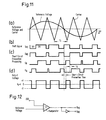
- FIG. 11 illustrates several waveforms that occur during a typical PWM operation.
- the illustration is in regard to only one phase, specifically the "U phase", of the three phases U, V and W relevant to the actual inverter operation in producing 3-phase A.C. power for operating a motor or like device.
- the triangular waveform output of the carrier generator 500 and the sinusoidal waveform output by the reference voltage generator 400 are shown superimposed in the same time frame.
- the superimposed waveforms illustrate a comparison between the reference voltage, which is used as a reference for the output voltage and the output frequency of the inverter, and the signal for modulating the reference voltage, e.g.
- Waveforms in Figure 11(b) are generated on the basis of the points of the waveforms of Figure 11(a) where the reference voltage waveform and the carrier cross.
- One of the waveforms in Figure 11(b) is a PWM signal U po This signal is generated for the upper side of the U phase and the signal is ON in the period in which the reference voltage is higher than the carrier voltage and OFF in the period in which the reference voltage is lower than that of the carrier.
- the other waveform in Figure 11(b) is a PWM signal U NO . This signal is generated for the lower side of the U phase and is obtained as the inversion of the signal U PO .
- the controllable element is actually driven by the PWM signals Up and Un, as seen in Figure 11(c), which signals are formed from waveforms U PO and U NO as subjected to a short circuit prevention process which delays the timing of the ON pulse by a time duration T d .
- T d the pulse-width modulated output voltage obtained as the U phase output is shown in Figure 11(d). Similar outputs are obtained for the V and W phases.
- the reference voltage waveform shown in Figure 11(a) which provides a reference for output frequency and output voltage, is delivered by the reference voltage waveform generator 400.
- the triangular carrier wave shown in Figure 11(a) is generated by the carrier generator 500.
- the PWM circuit 600 responds to the waveforns of Figure 11(a) and generates a PWM signal as shown in Figure 11(c).
- the driving circuit 700 amplifies the output of circuit 600 and drives the controllable element of the inversion converter 200 accordingly. Since the driving signal will vary with changes in the reference voltage waveform, an A.C. current may be obtained from the inverter with a variable voltage and a variable frequency.
- a high-speed switching element such as a power MOSFET, IGBT or the like, operable at a frequency between 10-20 Khz.
- the "ordinary loss” is the product of the current flowing during the ON time and the voltage drop
- the “switching loss” is the product of voltage and current at the time that the controllable element is turned ON and OFF.
- the total ordinary loss P ON is merely a function of current level (I)
- the total switching loss P SW is a function of current level (I) and the carrier frequency (f c ) which controls the switching of the element.
- the switching loss P SW is increased as the carrier frequency f c is increased. Also, the ratio of loss P ON : P SW is large when the current is near the level of the rated current of the inverter.
- inverter operation results in a relatively high switching loss, i.e ., high f c and high current, since proper thermal design of the switching element requires that its junction temperature be maintained below a given level, there is a significant cooling requirement.
- operation of the inverter at a high carrier frequency will reduce audible noise, but will require both an increase in the cooling capability and the size of the inverter.
- the noise produced poses a serious problem when an inverter-driven electric motor operates at low speed.
- the noise generated by the load driven by the motor is relatively low and the motor noise tends to be dominant.
- the noise generated by the load driven by the motor is increased so that the higher harmonic sounds produced by the electric motor are not dominant and their effect is not critical.
- f c is maintained high so that the loss is increased due to high switching losses.
- the conventional inverter In order to satisfy the thermal requirements of the switching element, the conventional inverter must be designed to maintain the temperature of the switching element below a maximum allowable temperature.
- the inverter can operate safely even when f c is kept high after an increase in the load.
- the most effective parameter available to contain the temperature below the maximum for the switching element is the carrier frequency f c . If carrier frequency f c is reduced to reduce the temperature rise due to switching power losses, however, it is difficult to effectively suppress the generation of audible noise.
- an object of the present invention is to provide an inverter apparatus which can operate with a lowered level of audible noise and which can compensate for increases in loss without requiring the size of the inverter to be increased or special cooling to be applied.
- a further object of the present invention is to control the carrier frequency in accordance with the inverter output frequency or the temperature of the controllable elements, or output current, so that the generation of noise is suppressed and the loss of power is reduced.
- the carrier frequency is variable within a range between an upper limit carrier frequency f c max, which is determined by the acceptable loss and the response time of the inverter, and a lower limit carrier frequency f c min, which is determined by the acceptable noise characteristic and distortion of the output current.
- the carrier frequency is controlled in accordance with the temperature of the controllable element of the inverter apparatus in such a manner that the carrier frequency is decreased and increased, respectively, as the detected temperature of the controllable element is increased and decreased.
- the carrier frequency is controlled in accordance with the output frequency of the inverter apparatus in such a manner that the carrier frequency is decreased and increased, respectively, as the inverter output frequency is increased and decreased.
- the carrier frequency may also be controlled in accordance with the output current of the inverter apparatus in such a manner that the carrier frequency is decreased and increased, respectively, as the inverter output current is increased and decreased.
- the carrier generator in the inverter apparatus of the present invention determines the carrier frequency in accordance with the temperature of the controllable element of the inverter or the output frequency or output current of the inverter. More specifically, the carrier frequency is increased when the detected temperature or the speed of the electric motor is low or the inverter output current is small, to thereby suppress noise generation, whereas when the detected temperature or the motor speed is increased or the inverter output current is large, the carrier frequency is decreased so as to reduce loss generated in the controllable element.
- numerals 100, 200, 300, 400, 600, 700 and 900 indicate elements which are the same or similar to those denoted by the same numerals in Figure 10, referring to the known inverter apparatus.
- Numeral 800 denotes a temperature detector for detecting the temperature of the controllable element and
- numeral 501 denotes a carrier generator that produces a signal with a frequency f c that is variable in response to the output of the temperature detector 800.
- the carrier frequency f c is controlled in a linear manner as shown in Figure 3, within a range between predetermined frequency limits f c max and f c min, in accordance with changes in temperature To, as represented by the output from the temperature detector 800.
- a carrier for example, a triangular waveform, is delivered to the PWM circuit at the controlled carrier frequency f c .
- FIG 2 shows another embodiment of the present invention.
- the elements of this embodiment are substantially the same as that shown in Figure 1 except that the temperature detector is removed and carrier generator 501 receives instead an input from the inverter output frequency setting device 900.
- the carrier frequency f c is controlled in a linear manner shown in Figure 4, within a range between predetermined frequency limits f c max and f c min, in accordance with changes in output frequency f o .
- the output frequency is set by an operator (i.e.
- Figure 12 shows a third embodiment in which the carrier frequency is controlled in accordance with the output from a current detector 1000, capable of detecting the load current on the inverter, within a range of low current I oc and high current I oH .
- the carrier frequency has an inverse linear relationship with the current within a range between predetermined frequencies f c max and f c min, (typically 15 Khz - 20 Khz) in a manner shown in Figure 13.
- the current detector 1000 may be a DCCT current detector which makes use of a Hall element. Although in Figure 13 the current detector 1000 is provided at the output side of the inverter, this is only illustrative and the current detector 1000 may be provided at any suitable portion where it can detect a current corresponding to the output current of the inverter.
- the motor which is the load on the inverter generates a higher-harmonic noise attributable to the carrier frequency f c .
- the effect of the noise can be avoided by increasing the carrier frequency f c to a level higher than the range of audible frequencies.
- Such a countermeasure causes a significant increase in the loss in the controllable element, causing a risk that the temperature T o of the controllable element will exceed the allowable upper limit value.
- T o Ta + T (2)
- Ta represents the temperature of the ambient air around the inverter
- T represents the temperature rise of the controllable element itself.
- T P x R th (3)
- P the loss of the controllable element
- R th the thermal resistance of the controllable element including its cooling means.
- the loss P generated in the controllable element can be expressed in terms of the steady loss P ON and switching loss P SW , wherein the steady loss P ON can be given as a function of the output current I O , while the switching loss P SW is a function of the output current I O and the carrier frequency f c .
- the loss P is changed in relation to the power P L supplied by the inverter to the load: namely, the smaller the power P L , the smaller the loss P.
- one aim of the use of an inverter of the type described resides in the reduction of energy consumption by reducing the power P L supplied to the load by reducing the output frequency f o of the inverter. In consequence, it is possible to reduce the loss P by reducing the output frequency f o and the loss P can be expressed as a function of the output frequency f o .
- T O T a + ⁇ P ON (I O , f o ) + P SW (I O , f c ) ⁇ x R th (4)
- the temperature T o of the controllable element can be determined when the ambient air temperature T a around the inverter, output current I O , output frequency f o and the carrier frequency f c are given.
- the parameters other than the carrier frequency f c are determined by the conditions and environment under which the inverter is used and, hence, cannot be controlled by the inverter itself.
- the temperature T O of the controllable element may rise as a result of one or both of the loss generated in the controllable element due to a change in the conditions or environment under which the inverter is used and a rise in the ambient air temperature around the inverter.
- the carrier frequency f c when the temperature T O approaches the maximum allowable temperature T R of the controllable element, the carrier frequency f c is lowered so as to maintain the temperature T O of the controllable element below the maximum allowable temperature T R .
- Figure 3 qualitatively illustrates the relationship between frequency and temperature and shows that frequency must be reduced to reduce the temperature.
- temperature is detected indirectly through detection of the output frequency f o and the output current I O .
- the control is not as accurate when compared with the method which relies upon the direct detection of the temperature T O of the controllable element.
- Such systems can be constructed with reduced cost because no temperature sensor is required.
- carrier generator 501 In Figure 5, the details of carrier generator 501 are shown.
- a reference voltage generator 3 whose output approximates a sine wave by, for example, quantization of an input analog signal with n-bit digital processing.
- Reference numeral 4 denotes a device for generating the upper limit value of a triangular wave carrier signal, having a controllable upper limit value, while numeral 5 denotes a device for generating the lower limit value of the triangular carrier signal.
- the devices 3 to 5 can be realized by the computing functions of a microcomputer 6, which may output respective voltage values in digital form.
- the microcomputer 6 may be a 16-bit microcomputer such as INTEL 8096 CPU, having a 16 bit data bus and incorporating an A/D converter.
- the voltage data derived from the microcomputer 6 are latched by flip-flops 7-9.
- the inverter of this embodiment is assumed to output 3-phase A.C. power so that flip-flops 7-9 latch voltages applicable to each of the U, V and W phases.
- Flip-flops 10 and 11 are connected to the microcomputer 6 for latching the upper and lower limit value data outputs from the limit generating elements 4 and 5, respectively.
- CS1, CS2, CS3, CS4 and CS5 represent control signals from the microcomputer 6 to the flip-flops 7 to 11.
- An n-bit up-and-down counter 12 is used for quantizing the triangular waveform generated by the carrier signal generator and outputting the quantized value.
- the triangular waveform is generated by counter 13, which repeats an up-count CKU and a down-count CKD in response to a clock input signal CK.
- Numerals 14 to 18 denote n-bit digital signal comparators. More specifically, the comparator 14 compares the n-bit U-phase voltage data from flip-flop 7 with the n-bit triangular wave data output by counter 12 and produces an output signal UP o in accordance with the result of the comparison.
- Comparator 17 is operative to compare the triangular wave data produced by the up-and-down counter 12 with the triangular wave upper limit data derived from the flip-flop 10 and delivers an output signal EQ u to the clock switching circuit 13.
- the output signals from the digital comparators 14, 15 and 16 which serve as signals for driving the switching elements of the U-, V- and W-phase are delivered to inversion circuits and short-circuit prevention circuits (not shown) in the manner illustrated for one of the phase signals in Figure 12.
- An output frequency setting device 1 and a temperature detector 2 are also seen in Figure 5, connected to microcomputer 6.
- the output frequency setting device 1 may output a signal in the form of voltage or current, based upon the operator's setting of a variable control contact in the device.
- the output frequency setting device 1 operates with a voltage signal.
- the temperature detector 2 for detecting the temperature of a switching element, e.g., a MOSFET or IGBT, outputs an analog signal, e.g, a voltage signal.
- the temperature detector may be a switch which is turned “on” and “off” when the temperature changes across a reference temperature.
- the output signal from the output frequency setting device 1 or the temperature detector 2 is delivered to the input port of the microcomputer 6.
- a voltage signal is input from the output frequency setting device 1
- a reference voltage corresponding to the output frequency is output from the microcomputer 6.
- the triangular wave upper and lower limit values which provide turning points of the triangular wave, are output from the microcomputer 6.
- the output signal from the output frequency setting device 1 or the temperature detector 2 is delivered to the input port of the microcomputer 6 which converts the thus input analog signal into a digital signal and calculates the upper and lower limit values of the reference voltage triangular wave. It is assumed here that the level of the output from the output frequency setting device 1 or temperature detection device 2 is constant.
- the microcomputer 6 can output a sine wave reference signal, quantized and approximated by an n-bit digital amount, as shown in Figure 6.
- the imaginary center of the amplitude of this sine wave resides between 200H and 1FFH in terms ot hexadecimal notation and the output sine wave changes its amplitude about this center of amplitude.
- the output frequency setting device 1 sets the output frequency of the inverter apparatus to a high level
- the sine waveform amplitude is increased.
- the output frequency is set to a low level
- the amplitude is decreased.
- the voltage signals computed and output by the microcomputer 6 are latched by flip-flops 7, 8 and 9, in correspondence with the voltages of the three phases U, V and W, respectively. These voltage data are set and latched at 120° intervals in terms of electric angle.
- the voltage data would be set through the 16-bit data bus of the microcomputer 6, when the size of the voltage data of each of U, V and W phases exceeds 5 bits, the voltage data cannot be set and latched in one operation, and the setting and latching has to be done in a plurality of operations. In such a case, the comparison of these voltage data with the triangular wave performed by the comparators is impeded due to the time difference existing between the voltage data for the three different phases. It is therefore necessary to provide an additional stage of flip-flops so as to enable the provision of voltage data for the U, V and W phases sinultaneously.
- the triangular wave upper and lower limit value data output from the microcomputer 6, as a result of functions 4 and 5, respectively, provide the turning points of the triangular wave generated by the triangular wave generator 12.
- the triangular wave upper limit value is latched by the flip-flop 10 and delivered to the comparator 17.
- the triangular wave lower limit value is latched by the flip-flop 11 and delivered to the comparator 18.
- the triangular wave generator 12 is an up-and-down counter which is controlled by up-counting clock CKU and down-counting clock CKD, and its current count is output simultaneously to comparators 14-18.
- the up-and-down counter 12 If the up-and-down counter 12 is in up-counting mode, it continues to count up in response to input clock signals CKU as seen by the ascending step waveform of Figure 7. However, when the triangular wave data constituted by n bits has become equal to the n-bit triangular wave upper limit value during the up-counting by the counter 12, the comparator 17 produces a coincidence signal EQU. In response to this signal EQU, the clock switching circuit 13 operates to set the up-count clock CKU in a non-active state and set the down-count clock CKD in an active state, so that the counter 12 is switched from up-counting mode to down-counting mode.
- the counter 12 When in the down-counting mode, the counter 12 counts down from its value at the turning point in stepped response to clock input CKD, as also seen in Figure 7.
- the comparator circuit 18 delivers a coincidence signal EQD.
- the clock switching circuit 13 operates so that the clock CKD and the clock CKU are switched into inactive and active states, respectively. The above-described operation is continually repeated so that a triangular wave signal is formed which has crests at the level of the triangular wave upper limit value and valleys at the level of the triangular wave lower limit value.
- Figure 8 shows an example of the construction of the clock switching circuit used in counter 13.
- the upper limit coincidence signal EQU and the lower limit coincidence signal EQD are amplified by amplifiers 131 and 132, respectively, and are input to set-reset type flip-flop 133.
- the Q output of the flip-flop is divided into two signals, one of which is inverted by inverter amplifier 134.
- a pair of logic gates 135 and 136 receive clock signal CK and each gate receives one of the Q signal and a signal which is the inversion of Q .
- the gates produce the clocks CKU and CKD.
- the frequency of the triangular wave is determined by the set values of the upper and lower limits and the frequency f ck of the clock CK with which frequency the up-and-down counter 12 performs its counting function.
- the following formula determines the frequency: If it is assumed that the triangular wave data is 10-bit data with upper and lower limit values of 3FFH and 000H in terms of hexadecimal notation, while the frequency f ck is 20 Mhz, the frequency of the triangular wave, i.e., the carrier frequency f c , is calculated from formula (5) as follows:
- the carrier frequency may be changed in accordance with the information from the output frequency setting device 1.
- the carrier frequency f c i.e ., the frequency of the triangular wave
- the carrier frequency f c can be controlled by varying the upper and lower limit values provided that the clock frequency f ck is constant. For instance, if the upper and lower limits are set to 2 FFH and 100H, respectively, the carrier frequency f c is calculated from formula (1) as follows:
- the carrier frequency f c by reducing the difference k between the upper and lower limit values. It is therefore possible to control the carrier frequency f c in relation to the output frequency of the inverter in such a manner that the carrier frequency f c is decreased and increased, respectively, in response to an increase and decrease in the inverter output frequency, by setting the output from the microcomputer 6 in such a manner as to decrease and increase the value of the difference k in response to increases and decreases in the inverter output frequency.
- the control of the carrier frequency f c in response to the detected temperature can be executed in the same manner. Namely, the temperature value input from temperature detector 1 can be used by microcomputer 6 to adjust the value k by adjusting either or both upper and lower limit values of the triangular waveform.
- the amplitude of the triangular wave is maintained constant so that the amplitude of the reference voltage is changed in proportion to the frequency of the reference voltage and delivered as the output from the inverter apparatus.
- the relationship between the voltage and the frequency of the A.C. power is determined by the amplitude of the triangular wave, the amplitude of the reference voltage and the frequency of the reference voltage.
- the amplitude of the triangular wave is changed in accordance with a change in the carrier frequency f c so that the amplitude of the reference voltage is also changed in order to maintain a constant relationship between the voltage and frequency of the output A.C. power of the inverter apparatus.
- each of the flip-flops 7 to 11 can be realized by D-type flip-flops 74HC74, each of the comparators 14 to 18 can be realized by a magnitude comparator 74HC85, and the up-and-down counter 12 can be realized by an up-and-down binary counter 74HC193.
- a change in the frequency of the triangular wave without being accompanied by a change in the amplitude can be realized simply by changing the clock frequency f ck .
- controllable elements While the temperature of the controllable elements is detected directly in the described embodiments, it may be more practical to detect the temperature of the surface of the cooling construction of the controllable elements or a part thereof, and to detect the ambient temperature of the inverter.
- the automatic control of carrier frequency in response to detected temperature can readily be achieved by microcomputer 6.
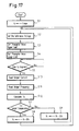
- Figure 15 schematically shows the flow of the process for changing the carrier frequency f c upon detection of the element temperature T O as performed by the microcomputer 6.
- the step START represents that the operation of the inverter is started. Considering that the element temperature T O is still low, f c max is set as the carrier frequency f c in Step S1. Taking into account the carrier frequency f c max, setting of the reference voltage, setting of the upper limit value of the triangular wave and the setting of the lower limit value are executed in Steps S2 to S4.
- Step S5 a time process is performed by a timer in which a time t1 has been set.
- the time t1 is determined on the basis of the thermal time constant of the controllable element including the cooling means of the controllable element.
- the element temperature T O is read in Step S6.
- Step S7 the element temperature T O is compared with the command temperature T.
- the command temperature T is a value obtained from the thermal design of the controllable element. In general, the command temperature T is set at a level which is obtained by de-rating the allowable maximum temperature T R to some extent.
- the carrier frequency f c is set in Step S8 to a level which is higher than the instant carrier frequency f c by f c .
- Steps S2 to S4 are executed again on the basis of the carrier frequency f c set in Step S8 or S9, and this operation is conducted repeatedly.
- Step S8 allows the operation of the inverter to continue by setting the frequency increment f c to zero, i.e ., maintaining the carrier frequency f c constantly at the level of the f c max.
- Step S9 the microcomputer judges that an abnormal temperature rise of the element is taking place, and skips to a protection process routine.
- Figure 16 quantitatively shows the manner in which the carrier frequency f c and the element temperature T O are changed in relation to the time t as a result of execution of the process described hereinabove.
- the described embodiment may be modified such that a tolerance T is imparted to the command temperature T so as to give a hysteresis effect to the control of the carrier frequency f c . It is also possible to compute the variance of the detected element temperature T O and to vary the carrier frequency increment f c in accordance with the variance of the element temperature.
- Figure 17 schematically shows the flow of the process performed by the microcomputer 6 for changing the carrier frequency f c on the basis of the output current I O and the output frequency f o .
- the process is materially the same as that shown in Figure 15 except that T o is computed from the detected values I O and f o of the output current and the output frequency instead of being detected directly.
Applications Claiming Priority (2)
| Application Number | Priority Date | Filing Date | Title |
|---|---|---|---|
| JP216479/89 | 1989-08-23 | ||
| JP1216479A JPH0382396A (ja) | 1989-08-23 | 1989-08-23 | パルス幅変調形インバータ装置 |
Publications (3)
| Publication Number | Publication Date |
|---|---|
| EP0413966A2 true EP0413966A2 (fr) | 1991-02-27 |
| EP0413966A3 EP0413966A3 (en) | 1991-04-03 |
| EP0413966B1 EP0413966B1 (fr) | 1993-10-06 |
Family
ID=16689084
Family Applications (1)
| Application Number | Title | Priority Date | Filing Date |
|---|---|---|---|
| EP90113857A Expired - Lifetime EP0413966B1 (fr) | 1989-08-23 | 1990-07-19 | Onduleur à modulation de largeur d'impulsions avec compensation de température |
Country Status (6)
| Country | Link |
|---|---|
| US (1) | US5068777A (fr) |
| EP (1) | EP0413966B1 (fr) |
| JP (1) | JPH0382396A (fr) |
| KR (1) | KR910005547A (fr) |
| CN (1) | CN1015849B (fr) |
| DE (1) | DE69003777T2 (fr) |
Cited By (12)
| Publication number | Priority date | Publication date | Assignee | Title |
|---|---|---|---|---|
| DE4116254A1 (de) * | 1990-05-18 | 1991-11-21 | Zexel Corp | Steuereinrichtung zum steuern eines buerstenlosen gleichstrommotors |
| DE10012084A1 (de) * | 2000-03-14 | 2001-09-20 | Wilo Gmbh | Verfahren zur Reduzierung der Schaltverluste |
| EP1148622A2 (fr) * | 2000-04-18 | 2001-10-24 | Mannesmann VDO Aktiengesellschaft | Procédé d'agencement d'un étage de sortie par modulation de largeur d'impulsion |
| GB2406006A (en) * | 2003-09-11 | 2005-03-16 | Bosch Gmbh Robert | Power control of an electric tool |
| WO2006006288A1 (fr) * | 2004-07-09 | 2006-01-19 | Matsushita Electric Industrial Co., Ltd. | Circuit inverseur et compresseur |
| WO2009087150A1 (fr) * | 2008-01-07 | 2009-07-16 | Woodward Seg Gmbh & Co. Kg | Procédé pour faire fonctionner un dispositif d'énergie éolienne |
| EP1850465A3 (fr) * | 2006-04-26 | 2010-07-14 | Nissan Motor Co., Ltd. | Contrôle d'un convertisseur de puissance par le changement de l'amplification de reglage de courant en fonction de la frequence porteuse |
| EP2544349A1 (fr) * | 2011-07-08 | 2013-01-09 | Siemens Aktiengesellschaft | Pilotage d'un convertisseur de courant pour installation de manutention |
| CN103267945A (zh) * | 2013-04-16 | 2013-08-28 | 上海电机系统节能工程技术研究中心有限公司 | 一种多功能变频电机试验用变频电源及波形产生方法 |
| GB2503779A (en) * | 2012-05-04 | 2014-01-08 | Control Tech Ltd | Method of controlling an inverter by temperature measurement and prediction employing variable frequency switching |
| US9083260B2 (en) | 2013-05-21 | 2015-07-14 | Control Techniques Limited | Inverter controller and method of controlling an inverter |
| EP3327918A4 (fr) * | 2015-07-17 | 2019-04-17 | Hitachi Industrial Equipment Systems Co., Ltd. | Dispositif de conversion de puissance et procédé de réduction du bruit de courant de sortie de celui-ci |
Families Citing this family (82)
| Publication number | Priority date | Publication date | Assignee | Title |
|---|---|---|---|---|
| JP2783623B2 (ja) * | 1989-12-04 | 1998-08-06 | 株式会社東芝 | インバータ装置 |
| JPH04168973A (ja) * | 1990-10-31 | 1992-06-17 | Toshiba Corp | 電源回路及びこれを用いた駆動回路 |
| US5309345A (en) * | 1990-11-13 | 1994-05-03 | Honda Giken Kogyo Kabushiki Kaisha | Invertor device |
| US5157594A (en) * | 1991-09-16 | 1992-10-20 | Sundstrand Corporation | Temperature-based inverter control system |
| US5495160A (en) * | 1993-12-06 | 1996-02-27 | Reliance Electric Company | Digital sine wave generator and motor controller |
| JP3301194B2 (ja) * | 1994-01-28 | 2002-07-15 | 三菱電機株式会社 | インバータ制御装置 |
| ATE183860T1 (de) * | 1994-06-03 | 1999-09-15 | Inventio Ag | Geräuscharmer betrieb einer von einem pulswechselrichter gespeisten maschine |
| EP0787973B1 (fr) * | 1995-08-17 | 2001-10-31 | Fanuc Ltd | Procede et appareil de traitement de donnees angulaires issues d'un codeur |
| AU2420697A (en) * | 1997-02-18 | 1998-09-08 | Steven Belyo | Improved motor control circuitry and circuitry enclosure |
| DE19920505B4 (de) * | 1999-05-05 | 2004-05-27 | Semikron Elektronik Gmbh | Umrichter mit Temperatursymmetrierung |
| JP3442340B2 (ja) * | 2000-03-29 | 2003-09-02 | ファナック株式会社 | モータ制御装置 |
| KR100395945B1 (ko) * | 2000-11-16 | 2003-08-27 | 주식회사 엘지이아이 | 인버터 공기조화기의 캐리어주파수제어방법 |
| JP2002218783A (ja) * | 2001-01-15 | 2002-08-02 | Rohm Co Ltd | モータ駆動装置 |
| JP2002272126A (ja) * | 2001-03-08 | 2002-09-20 | Daikin Ind Ltd | 空調機用インバータ制御方法およびその装置 |
| JP4045105B2 (ja) * | 2002-01-30 | 2008-02-13 | 株式会社日立産機システム | パルス幅変調方法、電力変換装置、およびインバータ装置 |
| US6535402B1 (en) * | 2002-07-12 | 2003-03-18 | Delta Electronics Inc. | Adaptive compensation of dead time for inverter and converter |
| JP2004208450A (ja) * | 2002-12-26 | 2004-07-22 | Sanden Corp | モータ制御装置 |
| JP2004274911A (ja) * | 2003-03-10 | 2004-09-30 | Denso Corp | モータ駆動装置 |
| JP3951975B2 (ja) * | 2003-07-22 | 2007-08-01 | 株式会社日立製作所 | 交流電動機の制御装置,交流電動機の制御方法及びモジュール |
| CN1319335C (zh) * | 2003-09-29 | 2007-05-30 | 浙江中控技术有限公司 | 实现冗余供电的以太网交换机及实现冗余供电的方法 |
| JP2006000731A (ja) * | 2004-06-16 | 2006-01-05 | Hitachi Koki Co Ltd | モータ制御装置および該制御装置を用いた遠心機 |
| JP4670413B2 (ja) * | 2004-07-07 | 2011-04-13 | トヨタ自動車株式会社 | 電源装置 |
| JP4622423B2 (ja) | 2004-09-29 | 2011-02-02 | 日本テキサス・インスツルメンツ株式会社 | パルス幅変調信号発生回路 |
| JP4665569B2 (ja) * | 2004-11-30 | 2011-04-06 | トヨタ自動車株式会社 | 電圧変換装置および電圧変換装置における電圧変換の制御をコンピュータに実行させるためのプログラムを記録したコンピュータ読取り可能な記録媒体 |
| DE112005000076B4 (de) * | 2005-02-17 | 2009-06-04 | General Motors Corp., Detroit | Verfahren und System zum Verwalten einer Prozessorausführungszeit unter Verwendung einer variablen Schaltfrequenz |
| JP4498967B2 (ja) * | 2005-04-01 | 2010-07-07 | 株式会社日本自動車部品総合研究所 | スイッチング装置 |
| KR100662434B1 (ko) * | 2005-11-17 | 2007-01-02 | 엘지전자 주식회사 | 세탁기의 구동 장치 및 이를 구비한 세탁기 |
| JP4848785B2 (ja) * | 2006-02-07 | 2011-12-28 | 株式会社明電舎 | インバータ装置の過負荷保護装置 |
| DE102006006960B4 (de) * | 2006-02-14 | 2021-02-18 | Sew-Eurodrive Gmbh & Co Kg | Verfahren und Elektro-Gerät |
| JP5050395B2 (ja) * | 2006-04-24 | 2012-10-17 | 日産自動車株式会社 | 電力制御装置及び電力制御方法 |
| JP4811102B2 (ja) * | 2006-04-26 | 2011-11-09 | 日産自動車株式会社 | 電力変換装置の制御装置および制御方法 |
| JP5239235B2 (ja) * | 2006-10-13 | 2013-07-17 | 日産自動車株式会社 | 電力変換装置および電力変換方法 |
| US7414375B2 (en) * | 2006-10-17 | 2008-08-19 | Zippy Technology Corp. | Fan voltage regulation control device |
| US7782005B2 (en) * | 2006-11-07 | 2010-08-24 | Nissan Motor Co., Ltd. | Power converter control |
| US7733674B2 (en) * | 2006-11-22 | 2010-06-08 | Nissan Motor Co., Ltd. | Power conversion apparatus for converting direct current to polyphase alternating current |
| TWI327811B (en) * | 2007-03-26 | 2010-07-21 | Delta Electronics Inc | Method of sampling and adjusting duty ratio |
| ES2385095T3 (es) * | 2007-04-20 | 2012-07-18 | Mitsubishi Electric Corporation | Controlador de inversor |
| JP4349447B2 (ja) * | 2007-07-19 | 2009-10-21 | トヨタ自動車株式会社 | インバータ制御装置および車両 |
| JP5055083B2 (ja) * | 2007-10-19 | 2012-10-24 | 日立コンピュータ機器株式会社 | デジタル制御電源装置 |
| US7652443B2 (en) | 2007-10-24 | 2010-01-26 | Gm Global Technology Operations, Inc. | Method and system for controlling a power inverter in electric drives |
| JP5115202B2 (ja) * | 2008-01-10 | 2013-01-09 | トヨタ自動車株式会社 | モータ駆動装置 |
| JP5188511B2 (ja) * | 2008-01-18 | 2013-04-24 | 三菱電機株式会社 | 電力変換器の制御装置 |
| KR101244588B1 (ko) * | 2008-04-28 | 2013-04-01 | 다이킨 고교 가부시키가이샤 | 인버터 제어장치 및 전력변환장치 |
| US8625315B2 (en) * | 2008-05-09 | 2014-01-07 | Etm Electromatic Inc | Inverter modulator with variable switching frequency |
| US8148929B2 (en) * | 2008-09-30 | 2012-04-03 | Rockwell Automation Technologies, Inc. | Power electronic module IGBT protection method and system |
| JP2010158088A (ja) * | 2008-12-26 | 2010-07-15 | Toyota Motor Corp | 車両およびその制御方法 |
| JP2011114984A (ja) * | 2009-11-27 | 2011-06-09 | Sanyo Electric Co Ltd | スイッチング制御回路、電源装置 |
| DE102009054987A1 (de) | 2009-12-18 | 2011-06-22 | HÜTTINGER Elektronik GmbH + Co. KG, 79111 | Verfahren zur Erzeugung von Wechselstromleistung |
| FR2961966B1 (fr) * | 2010-06-25 | 2012-07-13 | Valeo Sys Controle Moteur Sas | Procede de charge de moyens d'accumulation et dispositif de charge correspondant |
| JP2012135119A (ja) * | 2010-12-21 | 2012-07-12 | Sumitomo Heavy Ind Ltd | インバータ装置 |
| JP2012135118A (ja) * | 2010-12-21 | 2012-07-12 | Sumitomo Heavy Ind Ltd | インバータ装置 |
| TWI444806B (zh) * | 2011-01-31 | 2014-07-11 | Richtek Technology Corp | 適應性溫度補償電路及方法 |
| US8674651B2 (en) * | 2011-02-28 | 2014-03-18 | General Electric Company | System and methods for improving power handling of an electronic device |
| US20130343105A1 (en) * | 2011-03-16 | 2013-12-26 | Toyota Jidosha Kabushiki Kaisha | Inverter overheating protection control apparatus and inverter overheating protection control method |
| JP5802166B2 (ja) * | 2011-05-24 | 2015-10-28 | 株式会社デンソー | 電力変換装置 |
| CN102647147A (zh) * | 2011-12-26 | 2012-08-22 | 东方日立(成都)电控设备有限公司 | 一种自适应同步调制方法 |
| JP2013154680A (ja) * | 2012-01-27 | 2013-08-15 | Toyota Motor Corp | 車両接近報知装置 |
| US8974117B2 (en) * | 2012-04-04 | 2015-03-10 | Honeywell International Inc. | Pulse width modulation output digital temperature sensor device |
| DE102012212318A1 (de) * | 2012-07-13 | 2014-01-16 | Oerlikon Leybold Vacuum Gmbh | Verfahren zum Steuern einer Vakuumpumpe |
| TWI525973B (zh) * | 2012-11-02 | 2016-03-11 | 崇貿科技股份有限公司 | 具有溫度控制的電力轉換器的電路及其方法 |
| JP6201296B2 (ja) * | 2012-11-06 | 2017-09-27 | 富士電機株式会社 | 電力変換装置の制御装置 |
| US8994315B2 (en) * | 2013-03-06 | 2015-03-31 | Richtek Technology Corporation | Motor controller |
| JP6155779B2 (ja) * | 2013-04-09 | 2017-07-05 | 株式会社デンソー | パワー素子の電流検出回路 |
| US9318991B2 (en) * | 2013-04-11 | 2016-04-19 | The Boeing Company | Electric motor frequency modulation system |
| DE102013014480A1 (de) * | 2013-09-02 | 2015-03-05 | Minebea Co., Ltd. | Verfahren zum Betreiben eines Elektromotors |
| WO2015079569A1 (fr) * | 2013-11-29 | 2015-06-04 | 新電元工業株式会社 | Onduleur |
| WO2016002074A1 (fr) * | 2014-07-04 | 2016-01-07 | 三菱電機株式会社 | Convertisseur de courant, déshumidificateur, climatiseur et équipement de réfrigération |
| JP6156282B2 (ja) * | 2014-08-07 | 2017-07-05 | 株式会社デンソー | 回転機の制御装置 |
| JP6312852B2 (ja) * | 2014-11-04 | 2018-04-18 | 三菱電機株式会社 | 電動機駆動装置および空気調和機 |
| JP6091546B2 (ja) * | 2015-05-28 | 2017-03-08 | 三菱電機株式会社 | 回転電機制御装置 |
| JP6469864B2 (ja) * | 2015-07-10 | 2019-02-13 | 株式会社日立産機システム | 電力変換装置、及び、その温度低減方法 |
| JP6099724B1 (ja) * | 2015-11-10 | 2017-03-22 | 三菱電機株式会社 | 電動機制御装置 |
| DE102017113886A1 (de) | 2016-07-25 | 2018-01-25 | Schaeffler Technologies AG & Co. KG | Verfahren und Vorrichtung zur Anpassung einer Schaltfrequenz eines Inverters in einem elektrischen Antriebsstrang, insbesondere für ein Elektro- oder Hybridfahrzeug |
| CN106403486B (zh) * | 2016-09-02 | 2019-06-11 | 合肥美的电冰箱有限公司 | 变频制冷装置的控制方法、控制装置及冰箱 |
| DE102017202308A1 (de) * | 2017-02-14 | 2018-08-16 | Volkswagen Aktiengesellschaft | Verfahren zum Betreiben eines Inverters |
| DE102017207300A1 (de) | 2017-05-02 | 2018-11-08 | Robert Bosch Gmbh | Verfahren zur Ansteuerung eines Stromrichters, Steuervorrichtung für einen Stromrichter und Stromrichter |
| JP6993159B2 (ja) * | 2017-10-05 | 2022-01-13 | 大阪瓦斯株式会社 | 電力変換装置及び電力変換方法 |
| CN111381532B (zh) * | 2018-12-29 | 2021-12-03 | 重庆西山科技股份有限公司 | 频率控制装置及超声波换能器系统 |
| DE102020106758A1 (de) | 2020-03-12 | 2021-10-14 | Dr. Ing. H.C. F. Porsche Aktiengesellschaft | Elektromaschine |
| JP7019764B1 (ja) * | 2020-08-18 | 2022-02-15 | 三菱電機株式会社 | 交流回転機の制御装置及び電動車両 |
| CN112054744B (zh) * | 2020-09-18 | 2022-07-05 | 中国第一汽车股份有限公司 | 一种逆变器温度控制方法、系统、车辆及介质 |
| CN115308515B (zh) * | 2022-08-26 | 2024-02-20 | 天津电气科学研究院有限公司 | 一种igct三电平功率单元试验系统及方法 |
Citations (3)
| Publication number | Priority date | Publication date | Assignee | Title |
|---|---|---|---|---|
| EP0089627A2 (fr) * | 1982-03-18 | 1983-09-28 | Vee Arc Corporation | Modulation de porteuse asynchrone commandée |
| EP0198204A2 (fr) * | 1985-04-16 | 1986-10-22 | Sew-Eurodrive Gmbh & Co. | Procédé et dispositif pour convertir du courant continu en courant alternatif |
| US4688163A (en) * | 1986-07-01 | 1987-08-18 | Siemens Aktiengesellschaft | Method for controlling the phase angle of the output current or the output voltage of a frequency converter and apparatus for carrying out the method |
Family Cites Families (4)
| Publication number | Priority date | Publication date | Assignee | Title |
|---|---|---|---|---|
| JPS6028798A (ja) * | 1983-07-28 | 1985-02-13 | Mitsubishi Electric Corp | インバ−タ装置の運転方法 |
| DE3486449T2 (de) * | 1983-11-28 | 1997-11-27 | Matsushita Electric Ind Co Ltd | Pulsbreitenmodulationswechselrichtervorrichtung |
| JPS6292783A (ja) * | 1985-10-17 | 1987-04-28 | Toshiba Corp | 同期電動機のインバ−タ制御装置 |
| JPH0667207B2 (ja) * | 1986-05-28 | 1994-08-24 | 株式会社日立製作所 | 電力変換器の制御装置 |
-
1989
- 1989-08-23 JP JP1216479A patent/JPH0382396A/ja active Pending
-
1990
- 1990-07-14 CN CN90104701A patent/CN1015849B/zh not_active Expired
- 1990-07-19 DE DE90113857T patent/DE69003777T2/de not_active Expired - Fee Related
- 1990-07-19 EP EP90113857A patent/EP0413966B1/fr not_active Expired - Lifetime
- 1990-07-30 US US07/559,796 patent/US5068777A/en not_active Expired - Fee Related
- 1990-08-23 KR KR1019900013015A patent/KR910005547A/ko not_active Application Discontinuation
Patent Citations (3)
| Publication number | Priority date | Publication date | Assignee | Title |
|---|---|---|---|---|
| EP0089627A2 (fr) * | 1982-03-18 | 1983-09-28 | Vee Arc Corporation | Modulation de porteuse asynchrone commandée |
| EP0198204A2 (fr) * | 1985-04-16 | 1986-10-22 | Sew-Eurodrive Gmbh & Co. | Procédé et dispositif pour convertir du courant continu en courant alternatif |
| US4688163A (en) * | 1986-07-01 | 1987-08-18 | Siemens Aktiengesellschaft | Method for controlling the phase angle of the output current or the output voltage of a frequency converter and apparatus for carrying out the method |
Cited By (20)
| Publication number | Priority date | Publication date | Assignee | Title |
|---|---|---|---|---|
| DE4116254A1 (de) * | 1990-05-18 | 1991-11-21 | Zexel Corp | Steuereinrichtung zum steuern eines buerstenlosen gleichstrommotors |
| DE10012084A1 (de) * | 2000-03-14 | 2001-09-20 | Wilo Gmbh | Verfahren zur Reduzierung der Schaltverluste |
| EP1148622A2 (fr) * | 2000-04-18 | 2001-10-24 | Mannesmann VDO Aktiengesellschaft | Procédé d'agencement d'un étage de sortie par modulation de largeur d'impulsion |
| EP1148622A3 (fr) * | 2000-04-18 | 2002-10-02 | Siemens Aktiengesellschaft | Procédé d'agencement d'un étage de sortie par modulation de largeur d'impulsion |
| US6584792B2 (en) | 2000-04-18 | 2003-07-01 | Mannesmann Vdo Ag | Method for driving an output stage by pulse-width modulation |
| GB2406006A (en) * | 2003-09-11 | 2005-03-16 | Bosch Gmbh Robert | Power control of an electric tool |
| GB2406006B (en) * | 2003-09-11 | 2005-11-30 | Bosch Gmbh Robert | Power control device of an electric tool |
| US7075258B2 (en) | 2003-09-11 | 2006-07-11 | Robert Bosch Gmbh | Power control device of an electric tool, a method of power control of an electric tool and an electric tool provided with a power control device |
| WO2006006288A1 (fr) * | 2004-07-09 | 2006-01-19 | Matsushita Electric Industrial Co., Ltd. | Circuit inverseur et compresseur |
| US7400109B2 (en) | 2004-07-09 | 2008-07-15 | Matsushita Electric Industrial Co., Ltd. | Inverter circuit and compressor |
| EP1850465A3 (fr) * | 2006-04-26 | 2010-07-14 | Nissan Motor Co., Ltd. | Contrôle d'un convertisseur de puissance par le changement de l'amplification de reglage de courant en fonction de la frequence porteuse |
| WO2009087150A1 (fr) * | 2008-01-07 | 2009-07-16 | Woodward Seg Gmbh & Co. Kg | Procédé pour faire fonctionner un dispositif d'énergie éolienne |
| US8487461B2 (en) | 2008-01-07 | 2013-07-16 | Woodward Kempen | Method for operating a wind energy installation |
| EP2544349A1 (fr) * | 2011-07-08 | 2013-01-09 | Siemens Aktiengesellschaft | Pilotage d'un convertisseur de courant pour installation de manutention |
| EP2544349B1 (fr) | 2011-07-08 | 2018-09-19 | Siemens Aktiengesellschaft | Pilotage d'un convertisseur de courant pour installation de manutention |
| GB2503779A (en) * | 2012-05-04 | 2014-01-08 | Control Tech Ltd | Method of controlling an inverter by temperature measurement and prediction employing variable frequency switching |
| GB2503779B (en) * | 2012-05-04 | 2020-03-04 | Nidec Control Techniques Ltd | Inverter controller and method of controlling an inverter |
| CN103267945A (zh) * | 2013-04-16 | 2013-08-28 | 上海电机系统节能工程技术研究中心有限公司 | 一种多功能变频电机试验用变频电源及波形产生方法 |
| US9083260B2 (en) | 2013-05-21 | 2015-07-14 | Control Techniques Limited | Inverter controller and method of controlling an inverter |
| EP3327918A4 (fr) * | 2015-07-17 | 2019-04-17 | Hitachi Industrial Equipment Systems Co., Ltd. | Dispositif de conversion de puissance et procédé de réduction du bruit de courant de sortie de celui-ci |
Also Published As
| Publication number | Publication date |
|---|---|
| CN1015849B (zh) | 1992-03-11 |
| CN1049760A (zh) | 1991-03-06 |
| DE69003777T2 (de) | 1994-04-07 |
| EP0413966B1 (fr) | 1993-10-06 |
| KR910005547A (ko) | 1991-03-30 |
| US5068777A (en) | 1991-11-26 |
| JPH0382396A (ja) | 1991-04-08 |
| DE69003777D1 (de) | 1993-11-11 |
| EP0413966A3 (en) | 1991-04-03 |
Similar Documents
| Publication | Publication Date | Title |
|---|---|---|
| US5068777A (en) | Pulse width modulation type inverter having temperature compensation | |
| US6828752B2 (en) | Driving equipment and semiconductor equipment for alternating-current motor | |
| JP3178075B2 (ja) | 電力変換器の制御装置および電気車の制御装置 | |
| KR100240953B1 (ko) | 전력변환장치의 펄스폭 변조 방법 | |
| JPH09308256A (ja) | Pwmインバータ装置 | |
| JP3283134B2 (ja) | Pwmコンバータ装置 | |
| JPH0491698A (ja) | インバータ装置 | |
| JP2810081B2 (ja) | Pwm電力変換装置 | |
| KR940002232Y1 (ko) | 온도 보상을 가지는 펄스 폭 변조형 인버터장치 | |
| JP3299417B2 (ja) | インバータ装置 | |
| JP3286046B2 (ja) | 電力変換装置の制御方法 | |
| JPH02215996A (ja) | ターボ分子ポンプ駆動電源装置 | |
| JP2003125597A (ja) | 電気車の制御装置 | |
| JPS61203893A (ja) | Pwmインバ−タの変調方法 | |
| JP4649152B2 (ja) | 電力変換装置 | |
| US6018224A (en) | Anti-clipping circuit for induction motor drive system | |
| JP3261998B2 (ja) | インバータ制御装置 | |
| JP4277360B2 (ja) | 3レベルインバータの制御装置 | |
| JP3019931B2 (ja) | インバータ装置 | |
| JP2845543B2 (ja) | 電力変換装置 | |
| JP2659365B2 (ja) | パルス幅変調制御インバータの制御方法 | |
| JP3411995B2 (ja) | 電力変換装置 | |
| JPH05244775A (ja) | パルス幅変調インバータ装置 | |
| JPH08214555A (ja) | 3相電圧形インバータのためのpwm方法及び装置 | |
| JPH0323831Y2 (fr) |
Legal Events
| Date | Code | Title | Description |
|---|---|---|---|
| PUAI | Public reference made under article 153(3) epc to a published international application that has entered the european phase |
Free format text: ORIGINAL CODE: 0009012 |
|
| PUAL | Search report despatched |
Free format text: ORIGINAL CODE: 0009013 |
|
| 17P | Request for examination filed |
Effective date: 19901220 |
|
| AK | Designated contracting states |
Kind code of ref document: A2 Designated state(s): DE GB |
|
| AK | Designated contracting states |
Kind code of ref document: A3 Designated state(s): DE GB |
|
| 17Q | First examination report despatched |
Effective date: 19920210 |
|
| GRAA | (expected) grant |
Free format text: ORIGINAL CODE: 0009210 |
|
| AK | Designated contracting states |
Kind code of ref document: B1 Designated state(s): DE GB |
|
| REF | Corresponds to: |
Ref document number: 69003777 Country of ref document: DE Date of ref document: 19931111 |
|
| PLBE | No opposition filed within time limit |
Free format text: ORIGINAL CODE: 0009261 |
|
| STAA | Information on the status of an ep patent application or granted ep patent |
Free format text: STATUS: NO OPPOSITION FILED WITHIN TIME LIMIT |
|
| 26N | No opposition filed | ||
| REG | Reference to a national code |
Ref country code: GB Ref legal event code: 746 Effective date: 19950810 |
|
| PGFP | Annual fee paid to national office [announced via postgrant information from national office to epo] |
Ref country code: GB Payment date: 19960710 Year of fee payment: 7 |
|
| PGFP | Annual fee paid to national office [announced via postgrant information from national office to epo] |
Ref country code: DE Payment date: 19960726 Year of fee payment: 7 |
|
| PG25 | Lapsed in a contracting state [announced via postgrant information from national office to epo] |
Ref country code: GB Free format text: LAPSE BECAUSE OF NON-PAYMENT OF DUE FEES Effective date: 19970719 |
|
| GBPC | Gb: european patent ceased through non-payment of renewal fee |
Effective date: 19970719 |
|
| PG25 | Lapsed in a contracting state [announced via postgrant information from national office to epo] |
Ref country code: DE Free format text: LAPSE BECAUSE OF NON-PAYMENT OF DUE FEES Effective date: 19980401 |