EP0362974B1 - Ansteuerschaltung für ein Matrixanzeigegerät - Google Patents
Ansteuerschaltung für ein Matrixanzeigegerät Download PDFInfo
- Publication number
- EP0362974B1 EP0362974B1 EP89250049A EP89250049A EP0362974B1 EP 0362974 B1 EP0362974 B1 EP 0362974B1 EP 89250049 A EP89250049 A EP 89250049A EP 89250049 A EP89250049 A EP 89250049A EP 0362974 B1 EP0362974 B1 EP 0362974B1
- Authority
- EP
- European Patent Office
- Prior art keywords
- driving circuit
- period
- scanning
- voltage
- during
- Prior art date
- Legal status (The legal status is an assumption and is not a legal conclusion. Google has not performed a legal analysis and makes no representation as to the accuracy of the status listed.)
- Expired - Lifetime
Links
Images


Classifications
-
- G—PHYSICS
- G09—EDUCATION; CRYPTOGRAPHY; DISPLAY; ADVERTISING; SEALS
- G09G—ARRANGEMENTS OR CIRCUITS FOR CONTROL OF INDICATING DEVICES USING STATIC MEANS TO PRESENT VARIABLE INFORMATION
- G09G3/00—Control arrangements or circuits, of interest only in connection with visual indicators other than cathode-ray tubes
- G09G3/20—Control arrangements or circuits, of interest only in connection with visual indicators other than cathode-ray tubes for presentation of an assembly of a number of characters, e.g. a page, by composing the assembly by combination of individual elements arranged in a matrix no fixed position being assigned to or needed to be assigned to the individual characters or partial characters
- G09G3/34—Control arrangements or circuits, of interest only in connection with visual indicators other than cathode-ray tubes for presentation of an assembly of a number of characters, e.g. a page, by composing the assembly by combination of individual elements arranged in a matrix no fixed position being assigned to or needed to be assigned to the individual characters or partial characters by control of light from an independent source
- G09G3/36—Control arrangements or circuits, of interest only in connection with visual indicators other than cathode-ray tubes for presentation of an assembly of a number of characters, e.g. a page, by composing the assembly by combination of individual elements arranged in a matrix no fixed position being assigned to or needed to be assigned to the individual characters or partial characters by control of light from an independent source using liquid crystals
- G09G3/3611—Control of matrices with row and column drivers
- G09G3/3685—Details of drivers for data electrodes
- G09G3/3688—Details of drivers for data electrodes suitable for active matrices only
-
- G—PHYSICS
- G09—EDUCATION; CRYPTOGRAPHY; DISPLAY; ADVERTISING; SEALS
- G09G—ARRANGEMENTS OR CIRCUITS FOR CONTROL OF INDICATING DEVICES USING STATIC MEANS TO PRESENT VARIABLE INFORMATION
- G09G3/00—Control arrangements or circuits, of interest only in connection with visual indicators other than cathode-ray tubes
- G09G3/20—Control arrangements or circuits, of interest only in connection with visual indicators other than cathode-ray tubes for presentation of an assembly of a number of characters, e.g. a page, by composing the assembly by combination of individual elements arranged in a matrix no fixed position being assigned to or needed to be assigned to the individual characters or partial characters
- G09G3/34—Control arrangements or circuits, of interest only in connection with visual indicators other than cathode-ray tubes for presentation of an assembly of a number of characters, e.g. a page, by composing the assembly by combination of individual elements arranged in a matrix no fixed position being assigned to or needed to be assigned to the individual characters or partial characters by control of light from an independent source
- G09G3/36—Control arrangements or circuits, of interest only in connection with visual indicators other than cathode-ray tubes for presentation of an assembly of a number of characters, e.g. a page, by composing the assembly by combination of individual elements arranged in a matrix no fixed position being assigned to or needed to be assigned to the individual characters or partial characters by control of light from an independent source using liquid crystals
- G09G3/3611—Control of matrices with row and column drivers
- G09G3/3648—Control of matrices with row and column drivers using an active matrix
-
- G—PHYSICS
- G09—EDUCATION; CRYPTOGRAPHY; DISPLAY; ADVERTISING; SEALS
- G09G—ARRANGEMENTS OR CIRCUITS FOR CONTROL OF INDICATING DEVICES USING STATIC MEANS TO PRESENT VARIABLE INFORMATION
- G09G2310/00—Command of the display device
- G09G2310/02—Addressing, scanning or driving the display screen or processing steps related thereto
- G09G2310/0224—Details of interlacing
-
- G—PHYSICS
- G09—EDUCATION; CRYPTOGRAPHY; DISPLAY; ADVERTISING; SEALS
- G09G—ARRANGEMENTS OR CIRCUITS FOR CONTROL OF INDICATING DEVICES USING STATIC MEANS TO PRESENT VARIABLE INFORMATION
- G09G2310/00—Command of the display device
- G09G2310/02—Addressing, scanning or driving the display screen or processing steps related thereto
- G09G2310/0264—Details of driving circuits
- G09G2310/0297—Special arrangements with multiplexing or demultiplexing of display data in the drivers for data electrodes, in a pre-processing circuitry delivering display data to said drivers or in the matrix panel, e.g. multiplexing plural data signals to one D/A converter or demultiplexing the D/A converter output to multiple columns
Definitions
- This invention relates to a driving circuit for a matrix type display device such as a matrix type liquid crystal display device.
- Matrix type liquid crystal displays are beginning to match cathode-ray tubes in display quality as a result of a rapid advance in technology in recent years. Because of their excellent features such as thinness, light weight construction, and low power consumption, matrix type liquid crystal display devices are currently finding wide applications as display units for television receivers, visual display units for information processing apparatuses such as personal computers, and so on. An example of such a display and a circuit for driving it are disclosed in DE-A-3 702 335.
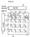
- FIG. 5 shows diagrammatically one example of a conventional matrix type liquid crystal display device.
- TFTs thin film transistors
- a TFT liquid crystal panel 100 comprises liquid crystal picture elements (hereinafter abbreviated as "pixels") 103 disposed in a matrix form of n rows and m columns.
- Each pixel 103 includes a pixel electrode 106, a counter electrode 105, and a liquid crystal layer 107 sandwiched between the two electrodes.
- the equivalent circuit of the pixel consists of a capacitor as shown in Fig. 5.
- the counter electrode 105 is usually a conductive layer disposed common to all the pixel electrodes 106.
- each pixel 103 Disposed adjacent to each pixel 103 is a TFT 104, the drain electrode of which is connected to the pixel electrode 106.
- TFT liquid crystal panel 100 In the TFT liquid crystal panel 100 are disposed scanning lines 101 (the number of which is n) which are parallel to one another.
- the gate electrodes (switching terminals) of the TFTs 104 on the jth row are connected.
- Signal lines 102 (the number of which is m) are disposed in such a way as to intersect perpendicularly with the scanning lines 101.
- the source electrodes (signal terminals) of the TFTs 104 on the ith column are connected.
- the TFT liquid crystal panel 100 is driven by a driving circuit which includes a gate driver 200 and a source driver 300.
- the gate driver 200 and the source driver 300 are connected to the scanning lines 101 and the signal lines 102, respectively.
- a video signal is input to the source driver 300.
- Control signals such as scanning pulses to the gate driver 200 and sampling clock pulses to the source driver 300 are supplied from a control circuit (not shown).
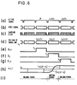
- Figure 6 shows an example of display timing within one field or one frame in the matrix type liquid crystal display device of Fig. 5.
- the source driver 300 samples the video signal which is serially input during each horizontal scanning period initiated by a horizontal synchronizing pulse ((a) and (b) of Fig. 6).
- the gate driver 200 applies a pulse to the jth scanning line during the (j+1)th horizontal scanning period (j+1)H (in Fig.
- the voltage written therein is held over a given period of time.
- the voltage applied in each field or frame has the opposite polarity from that applied in the preceding field or frame. That is, an alternating-current driving method is used in which two fields or two frames make up one complete alternating-current cycle.
- the use of the alternating-current driving is to prevent the pixel 103 from deteriorating due to the application of a direct current voltage.
- a cathode-ray tube two methods are available for displaying an image by the driving circuit on a matrix type liquid crystal display device, i.e. the interlaced scanning method and the non-interlaced scanning method.
- one frame consists of an odd field corresponding to the odd scanning lines 101 and an even field corresponding to the even scanning lines 101, and the scanning for the odd field and that for even field are alternately performed.
- Interlaced scanning is used in the NTSC (National Television System Committee TV) system.
- the voltage e(2k-1, i) written into the pixels 103 of the odd columns in the odd field is held throughout the scanning period for the immediately succeeding even field ((e) of Fig. 8).
- the voltage e(2k, i) written into the pixels 103 of the even columns in the even field is held throughout the scanning period for the immediately succeeding odd field ((h) of Fig.
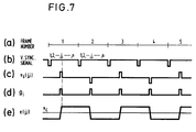
- the matrix liquid crystal display device requires the provision of a frame memory or a field memory for storing sampled video signals. It further requires the provision of a high-speed A/D converter and a circuit for three-dimensional signal processing. Furthermore, since the number of the scanning lines to be scanned during one field in the non-interlaced scanning method is twice as many compared with that in the interlaced scanning method, the non-interlaced scanning system must be provided with a high-speed driving circuit including a source driver and gate driver, and with a liquid crystal panel which is capable of high-speed operation. Even if the non-interlaced scanning method is applied to a matrix type liquid crystal display device using existing techniques, however, both the driving circuit and the display device would be extremely expensive.
- the driving circuit for a matrix type display device of this invention which overcomes the above-discussed and numerous other disadvantages and deficiencies of the prior art, which device comprises picture elements arranged in a matrix, switching elements connected respectively to said picture elements, scanning lines each of which is connected to a switching terminal of switching elements which are arranged in one direction, and signal lines each of which is connected to a signal terminal of switching elements which are arranged in a direction crossing said one direction, the driving circuit comprises: a first driving means for, during a writing period, selectively driving any one or more scanning line included in a group of scanning lines which correspond to the field to be scanned, and for, during an erasing period, selectively driving at least one scanning line included in another group of scanning lines which do not correspond to the field to be scanned, said writing period and said erasing period sharing one horizontal scanning period; and a second driving means for, during said writing period, applying a signal voltage the level of which corresponds to a video signal, to said signal lines, and for, during said erasing period, applying
- the writing period precedes said erasing period in one horizontal scanning period.
- the picture elements comprises a liquid crystal.
- the switching elements are thin film transistors.
- the switching terminal is a gate of said thin film transistors, and said signal terminal a source of said thin film transistors.
- Figure 1 is a block diagram illustrating a driving circuit according to the invention.
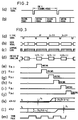
- Figure 2 illustrates schematically a writing period and an erasing period formed in one horizontal scanning period in the driving circuit of Fig. 1.
- Figure 3 is a timing chart showing the display timing in one odd field in the driving circuit of Fig. 1.
- Figure 4 is a timing chart showing the voltage application over a plurality of fields in the driving circuit of Fig. 1.
- Figure 5 is a block diagram illustrating a conventional driving circuit.
- Figure 6 is a timing chart showing the display timing in one odd field in the driving circuit of Fig. 5.
- Figure 7 is a timing chart showing the voltage application over a plurality of fields in the driving circuit of Fig. 5 when the non-interlaced method is employed.
- Figure 8 is a timing chart showing the voltage application over a plurality of fields in the driving circuit of Fig. 5 when the interlaced method is employed.
- Figure 9 illustrates the still picture and moving picture in a conventional matrix type liquid crystal display device.
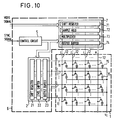
- Figure 10 is a block diagram illustrating another driving circuit according to the invention.
- FIG. 1 is a block diagram of a matrix type liquid crystal display device provided with a driving circuit according to the invention.
- a TFT liquid crystal panel 1 has the same construction as the conventional one shown in Fig. 5.
- a driving circuit 6 comprises a gate driver 2, two source drivers 3 and 4, and a control circuit 5 for controlling these drivers.
- the control circuit 5 generates control signals in response to the synchronizing signals input from an external source and feeds them to the gate driver 2 and the source drivers 3 and 4.
- the control signals include scanning pulses supplied to the gate driver 2, and sampling clock pulses supplied to the source drivers 3 and 4.
- the gate driver 2 comprises a shift register 21, a level shifter 22, and an output buffer 23.
- the output buffer 23 is connected to scanning lines 11 of the TFT liquid crystal panel 1.
- the source driver 3 comprises a shift register 31, a sample hold circuit 32, a multiplexer 33, and an output buffer 34.
- the source driver 4 comprises a shift register 41, a sample hold circuit 42, a multiplexer 43, and an output buffer 44. Both the output buffers 34 and 44 are connected to the signal lines 12 of the TFT liquid crystal panel 1. Video signals are supplied to both the source drivers 3 and 4.
- the driving circuit 6 drives the TFT liquid crystal panel 1 by using the interlaced scanning method in which the scanning is alternately performed for the odd and even fields.
- a writing period and an erasing period are provided in each horizontal scanning period on a time-sharing basis, as shown in Fig. 2. The operation of the driving circuit 6 will be described.
- Figure 3 shows a display timing in the case where the odd field is displayed in the matrix type liquid crystal display device of Fig. 1.
- the video signals serially input are sampled and held by the shift register 31 and sample hold circuit 32 of the source driver 3 for the odd field.
- the gate driver 2 applies a pulse to the (2k-1)th scanning line 11 during the above writing period in the horizontal scanning period (k+1)H (in Fig. 3, "g 2k " indicates the voltage applied to the 2kth scanning line 11).
- a voltage e(2k-1, i) applied to the pixel connected to the transistor (2k-1, i) is given as the difference between the voltage v s (2k-1, i) and a voltage vc applied to a counter electrode 15, i.e. v s (2k-1, i) - vc ((k) of Fig. 3). The writing is thus performed.
- the gate driver 2 applies a pulse to the 2kth scanning line adjacent to the (2k-1)th scanning line 11 chosen during the writing period in the same horizontal scanning period ((1) of Fig. 3).
- a voltage as to make the voltage v e applied to the pixel below the threshold value of the pixel is applied to the signal lines 12 through the output buffer 44 of the source driver 4 for the even field. That is, a voltage close to the voltage v c applied to the counter electrode 15 is chosen for application to the signal lines 12 during the erasing period. This puts the pixels on the 2kth scanning line 11 in an erased state.
- the multiplexers 33 and 43 are provided to select the voltage output from the sample hold circuits 32 and 42 and the voltage for putting the pixels in an erased state, in accordance with the control signals supplied from the control circuit 5, to feed them to the output buffers 34 and 44, respectively.
- the timing pulse shown in (m) of Fig. 3 is supplied to the gate driver 2 and the source drivers 3 and 4 to control the writing period and erasing period.
- the manner of time sharing one horizontal scanning period into the writing and erasing periods and their sequence may be adequately determined by considering the characteristics of the pixel and other factors.
- the gate driver 2 drives the even scanning lines 11 during the writing period and the odd scanning lines 11 during the erasing period.
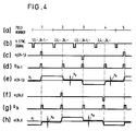
- Figure 4 illustrates the voltage application to the pixels covering a plurality of fields.
- the writing is performed during the scanning period for an odd field, and the erasure during the scanning period for an even field.
- the operation is reversed for the pixels on the even columns.
- the driving circuit 6 of this embodiment serves to substantially shorten the period to hold the voltage for the pixels, simultaneously, on the odd and even columns, and, therefore, helps to greatly improve the image quality even when displaying a moving picture.
- the driving-circuit shown in Fig. 1 comprises two source drivers 3 and 4 which function in odd fields and even fields, respectively.
- the present invention is not restricted to the above.
- Figure 10 is a block diagram of a matrix type liquid crystal display device provided with another driving circuit according to the invention.
- the driving circuit shown in Fig. 10 comprises a sole source driver 7.
- the source driver 7 comprises a shift register 71, a sample hold circuit 72, a multiplexer 73, and an output buffer 74.
- the source driver 7 functions as the combination of the source drivers 3 and 4 shown in Fig. 1, that is, the source driver 7 of this embodiment performs the timing control of Fig. 3 in both odd fields and even fields.
- the operation of the driving circuit shown in Fig. 10 will be apparent for those skilled in the art from the description of the driving circuit shown in Fig. 1, and, therefore, its detailed description is omitted.
- the present invention is not restricted to a driving circuit for the 2:1 interlaced scanning as is used in the NTSC system.
Landscapes
- Engineering & Computer Science (AREA)
- Chemical & Material Sciences (AREA)
- Crystallography & Structural Chemistry (AREA)
- Physics & Mathematics (AREA)
- Computer Hardware Design (AREA)
- General Physics & Mathematics (AREA)
- Theoretical Computer Science (AREA)
- Liquid Crystal Display Device Control (AREA)
- Liquid Crystal (AREA)
Claims (5)
- Treiberschaltung für ein Matrixanzeigegerät, wobei das Gerät Bildelemente aufweist, die in einer Matrix angeordnet sind, Schaltelemente, die jeweils mit den Bildelementen verbunden sind, Abfrageleitungen, von denen jede mit einem Schalteranschluß der Schaltelemente verbunden ist, welche in einer Richtung angeordnet sind, und Signalleitungen, von denen jede mit einem Signalanschluß der Schaltelemente verbunden ist, welche in einer Richtung angeordnet sind, die die besagte eine Richtung kreuzt wobei die Ansteuerschaltung aufweist:
eine erste Treibereinrichtung, um während einer Schreibperiode wahlweise eine oder mehrere Abfrageleitungen anzusteuern, die in einer Gruppe von Abfrageleitungen enthalten sind, die dem abzufragenden Feld entsprechen, und um während einer Löschperiode wahlweise mindestens eine Abfrageleitung anzusteuern, die in einer anderen Gruppe von Abfrageleitungen enthalten ist, die nicht dem abzufragenden Feld entsprechen, wobei sich die Schreibperiode und die Löschperiode eine horizontale Abfrageperiode teilen; und
eine zweite Treibereinrichtung, um während der Schreibperiode eine Signalspannung, deren Pegel dem eines Videosignals entspricht, auf die Signalleitungen zu legen, und um während der Löschperiode eine Spannung auf die Signalleitungen zu legen, damit die Spannung, die an den Bildelementen liegt, auf einen Pegel unterhalb des Grenzwertpegels der Bildschirmelemente gesetzt wird. - Treiberschaltung nach Anspruch 1, wobei die Schreibperiode der Löschperiode in einer horizontalen Abfrageperiode vorausgeht.
- Treiberschaltung nach Anspruch 1, wobei die Bildelemente einen Flüssigkristall aufweisen.
- Treiberschaltung nach Anspruch 1, wobei die Schaltelemente Dünnfilmtransistoren sind.
- Treiberschaltung nach Anspruch 4, wobei der Schalteranschluß ein Gate der Dünnschichttransistoren und der Signalanschluß eine Source der Dünnschichttransistoren ist.
Applications Claiming Priority (2)
| Application Number | Priority Date | Filing Date | Title |
|---|---|---|---|
| JP250349/88 | 1988-10-04 | ||
| JP25034988 | 1988-10-04 |
Publications (3)
| Publication Number | Publication Date |
|---|---|
| EP0362974A2 EP0362974A2 (de) | 1990-04-11 |
| EP0362974A3 EP0362974A3 (de) | 1991-10-23 |
| EP0362974B1 true EP0362974B1 (de) | 1995-01-11 |
Family
ID=17206594
Family Applications (1)
| Application Number | Title | Priority Date | Filing Date |
|---|---|---|---|
| EP89250049A Expired - Lifetime EP0362974B1 (de) | 1988-10-04 | 1989-10-03 | Ansteuerschaltung für ein Matrixanzeigegerät |
Country Status (3)
| Country | Link |
|---|---|
| US (1) | US5412397A (de) |
| EP (1) | EP0362974B1 (de) |
| DE (1) | DE68920531T2 (de) |
Families Citing this family (32)
| Publication number | Priority date | Publication date | Assignee | Title |
|---|---|---|---|---|
| EP0559321B1 (de) * | 1992-01-31 | 1997-07-09 | Canon Kabushiki Kaisha | Flüssigkristall-Lichtventil mit aktiver Matrix und Treiberschaltung |
| JP3582082B2 (ja) | 1992-07-07 | 2004-10-27 | セイコーエプソン株式会社 | マトリクス型表示装置,マトリクス型表示制御装置及びマトリクス型表示駆動装置 |
| JP3133216B2 (ja) * | 1993-07-30 | 2001-02-05 | キヤノン株式会社 | 液晶表示装置及びその駆動方法 |
| TW255032B (de) * | 1993-12-20 | 1995-08-21 | Sharp Kk | |
| TW277129B (de) * | 1993-12-24 | 1996-06-01 | Sharp Kk | |
| KR0171913B1 (ko) * | 1993-12-28 | 1999-03-20 | 사토 후미오 | 액정표시장치 및 그 구동방법 |
| GB2295045B (en) * | 1994-11-08 | 1998-07-15 | Citizen Watch Co Ltd | A liquid crystal display device and a method of driving the same |
| CN100530332C (zh) * | 1995-02-01 | 2009-08-19 | 精工爱普生株式会社 | 液晶显示装置 |
| JPH08227283A (ja) * | 1995-02-21 | 1996-09-03 | Seiko Epson Corp | 液晶表示装置、その駆動方法及び表示システム |
| JPH08234703A (ja) * | 1995-02-28 | 1996-09-13 | Sony Corp | 表示装置 |
| US5710571A (en) * | 1995-11-13 | 1998-01-20 | Industrial Technology Research Institute | Non-overlapped scanning for a liquid crystal display |
| KR100205259B1 (ko) * | 1996-03-04 | 1999-07-01 | 구자홍 | 액티브매트릭스 액정디스플레이의 구동회로 |
| US5903250A (en) * | 1996-10-17 | 1999-05-11 | Prime View International Co. | Sample and hold circuit for drivers of an active matrix display |
| JP3827823B2 (ja) | 1996-11-26 | 2006-09-27 | シャープ株式会社 | 液晶表示画像の消去装置及びそれを備えた液晶表示装置 |
| KR100204909B1 (ko) * | 1997-02-28 | 1999-06-15 | 구본준 | 엘씨디 소스 드라이버 |
| JP2000227784A (ja) * | 1998-07-29 | 2000-08-15 | Seiko Epson Corp | 電気光学装置の駆動回路および電気光学装置 |
| US20020149556A1 (en) * | 1998-09-14 | 2002-10-17 | Seiko Epson Corporation | Liquid crystal display apparatus, driving method therefor, and display system |
| JP3185778B2 (ja) * | 1999-02-10 | 2001-07-11 | 日本電気株式会社 | アクティブマトリクス型液晶表示装置、その製造方法及びその駆動方法 |
| JP3712046B2 (ja) * | 2000-05-30 | 2005-11-02 | 富士通株式会社 | 液晶表示装置 |
| KR100367014B1 (ko) * | 2000-12-29 | 2003-01-09 | 엘지.필립스 엘시디 주식회사 | 액정 표시장치 및 그 구동방법 |
| KR100783700B1 (ko) * | 2001-02-14 | 2007-12-07 | 삼성전자주식회사 | 임펄스 구동 방식을 갖는 액정 표시 장치와 이의 구동 장치 |
| JP3791355B2 (ja) * | 2001-06-04 | 2006-06-28 | セイコーエプソン株式会社 | 駆動回路、及び駆動方法 |
| JP4566459B2 (ja) * | 2001-06-07 | 2010-10-20 | 株式会社日立製作所 | 表示装置 |
| US7411573B2 (en) * | 2001-06-08 | 2008-08-12 | Thomson Licensing | LCOS column memory effect reduction |
| JP4011320B2 (ja) | 2001-10-01 | 2007-11-21 | 株式会社半導体エネルギー研究所 | 表示装置及びそれを用いた電子機器 |
| KR100840675B1 (ko) * | 2002-01-14 | 2008-06-24 | 엘지디스플레이 주식회사 | 액정표시장치의 데이터 구동 장치 및 방법 |
| JP2004070293A (ja) * | 2002-06-12 | 2004-03-04 | Seiko Epson Corp | 電子装置、電子装置の駆動方法及び電子機器 |
| JP2004198493A (ja) * | 2002-12-16 | 2004-07-15 | Seiko Epson Corp | 電子回路の駆動方法、電子装置の駆動方法、電気光学装置の駆動方法及び電子機器 |
| TW566416U (en) * | 2003-04-22 | 2003-12-11 | Shi-Tsai Chen | Air expanding shaft |
| KR100582381B1 (ko) * | 2004-08-09 | 2006-05-22 | 매그나칩 반도체 유한회사 | 소스 드라이버 및 드라이버 내에서 수행되는 화상 데이터압축 전송 방법 |
| JP2006343625A (ja) * | 2005-06-10 | 2006-12-21 | Nec Electronics Corp | 液晶表示装置および液晶表示装置のデータ線駆動回路 |
| US8174480B2 (en) * | 2008-06-12 | 2012-05-08 | Himax Technologies Limited | Gate driver and display panel utilizing the same |
Family Cites Families (10)
| Publication number | Priority date | Publication date | Assignee | Title |
|---|---|---|---|---|
| JPS6056026B2 (ja) * | 1976-09-20 | 1985-12-07 | 松下電器産業株式会社 | 液晶パネルの駆動方式 |
| US4481511A (en) * | 1981-01-07 | 1984-11-06 | Hitachi, Ltd. | Matrix display device |
| JPH07118794B2 (ja) * | 1983-03-16 | 1995-12-18 | シチズン時計株式会社 | 表示装置 |
| AU552858B2 (en) * | 1983-06-06 | 1986-06-26 | Stc Plc | Scanning liquid crystal dispaly cells |
| JPH0652938B2 (ja) * | 1986-01-28 | 1994-07-06 | 株式会社精工舎 | 液晶表示装置 |
| DE3884442T2 (de) * | 1987-04-15 | 1994-02-17 | Sharp Kk | Flüssigkristallanzeigegerät. |
| EP0291252A3 (de) * | 1987-05-12 | 1989-08-02 | Seiko Epson Corporation | Verfahren und Gerät zur Fernsehwiedergabe |
| US4845482A (en) * | 1987-10-30 | 1989-07-04 | International Business Machines Corporation | Method for eliminating crosstalk in a thin film transistor/liquid crystal display |
| JPH02157813A (ja) * | 1988-12-12 | 1990-06-18 | Sharp Corp | 液晶表示パネル |
| DE4201960A1 (de) * | 1992-01-23 | 1993-07-29 | Gerb Schwingungsisolierungen | Federanordnung zur herabsetzung von koerperschall |
-
1989
- 1989-10-03 EP EP89250049A patent/EP0362974B1/de not_active Expired - Lifetime
- 1989-10-03 DE DE68920531T patent/DE68920531T2/de not_active Expired - Lifetime
-
1994
- 1994-01-03 US US08/177,202 patent/US5412397A/en not_active Expired - Lifetime
Also Published As
| Publication number | Publication date |
|---|---|
| DE68920531D1 (de) | 1995-02-23 |
| EP0362974A3 (de) | 1991-10-23 |
| US5412397A (en) | 1995-05-02 |
| EP0362974A2 (de) | 1990-04-11 |
| DE68920531T2 (de) | 1995-05-04 |
Similar Documents
| Publication | Publication Date | Title |
|---|---|---|
| EP0362974B1 (de) | Ansteuerschaltung für ein Matrixanzeigegerät | |
| JP2833546B2 (ja) | 液晶表示装置 | |
| US7148885B2 (en) | Display device and method for driving the same | |
| US6211851B1 (en) | Method and apparatus for eliminating crosstalk in active matrix liquid crystal displays | |
| US5767832A (en) | Method of driving active matrix electro-optical device by using forcible rewriting | |
| EP0313876B1 (de) | Verfahren zum Eliminieren des Übersprechens in einer Dünnfilmtransistor-Flüssigkristallanzeigeeinrichtung | |
| EP0216188B1 (de) | Rasteranzeigetafel | |
| KR950013444B1 (ko) | 액정 표시장치 | |
| US7221344B2 (en) | Liquid crystal display device and driving control method thereof | |
| US6232945B1 (en) | Display device and its driving method | |
| US5777591A (en) | Matrix display apparatus employing dual switching means and data signal line driving means | |
| JPH09329807A (ja) | 液晶表示装置 | |
| JP3305931B2 (ja) | 液晶表示装置 | |
| US5448385A (en) | Active matrix liquid crystal display device with interdigitated counter electrodes | |
| JPH07140933A (ja) | 液晶表示装置の駆動方法 | |
| JPH02210985A (ja) | マトリクス型液晶表示装置の駆動回路 | |
| JPH10233981A (ja) | ディスプレイ装置及びディスプレイ走査方法 | |
| JPH0754420B2 (ja) | 液晶表示装置の駆動方法 | |
| JPH0854601A (ja) | アクティブマトリクス型液晶表示装置 | |
| EP0478382A2 (de) | Verfahren und Einrichtung zum Steuern eines Flüssigkristallanzeigegeräts | |
| JPH06101830B2 (ja) | 画像表示方式 | |
| JPH02113294A (ja) | 液晶表示装置 | |
| JPH0697381B2 (ja) | アクテイブマトリクス型表示装置の駆動方法 | |
| JP2525344B2 (ja) | マトリクス表示パネル | |
| CN118298749A (zh) | 显示装置 |
Legal Events
| Date | Code | Title | Description |
|---|---|---|---|
| PUAI | Public reference made under article 153(3) epc to a published international application that has entered the european phase |
Free format text: ORIGINAL CODE: 0009012 |
|
| AK | Designated contracting states |
Kind code of ref document: A2 Designated state(s): DE FR |
|
| 17P | Request for examination filed |
Effective date: 19901221 |
|
| PUAL | Search report despatched |
Free format text: ORIGINAL CODE: 0009013 |
|
| AK | Designated contracting states |
Kind code of ref document: A3 Designated state(s): DE FR |
|
| 17Q | First examination report despatched |
Effective date: 19931206 |
|
| GRAA | (expected) grant |
Free format text: ORIGINAL CODE: 0009210 |
|
| AK | Designated contracting states |
Kind code of ref document: B1 Designated state(s): DE FR |
|
| REF | Corresponds to: |
Ref document number: 68920531 Country of ref document: DE Date of ref document: 19950223 |
|
| ET | Fr: translation filed | ||
| PLBE | No opposition filed within time limit |
Free format text: ORIGINAL CODE: 0009261 |
|
| STAA | Information on the status of an ep patent application or granted ep patent |
Free format text: STATUS: NO OPPOSITION FILED WITHIN TIME LIMIT |
|
| 26N | No opposition filed | ||
| PGFP | Annual fee paid to national office [announced via postgrant information from national office to epo] |
Ref country code: FR Payment date: 19971009 Year of fee payment: 9 |
|
| PG25 | Lapsed in a contracting state [announced via postgrant information from national office to epo] |
Ref country code: FR Free format text: LAPSE BECAUSE OF NON-PAYMENT OF DUE FEES Effective date: 19990630 |
|
| REG | Reference to a national code |
Ref country code: FR Ref legal event code: ST |
|
| PGFP | Annual fee paid to national office [announced via postgrant information from national office to epo] |
Ref country code: DE Payment date: 20081014 Year of fee payment: 20 |