EP0348992A2 - Gerät und Verfahren zum Nachweis von Mustern, die auf einem Transmissions-Rasterelektronenmikroskop basiert sind - Google Patents
Gerät und Verfahren zum Nachweis von Mustern, die auf einem Transmissions-Rasterelektronenmikroskop basiert sind Download PDFInfo
- Publication number
- EP0348992A2 EP0348992A2 EP89111920A EP89111920A EP0348992A2 EP 0348992 A2 EP0348992 A2 EP 0348992A2 EP 89111920 A EP89111920 A EP 89111920A EP 89111920 A EP89111920 A EP 89111920A EP 0348992 A2 EP0348992 A2 EP 0348992A2
- Authority
- EP
- European Patent Office
- Prior art keywords
- electron beam
- pattern
- detected
- image
- signal
- Prior art date
- Legal status (The legal status is an assumption and is not a legal conclusion. Google has not performed a legal analysis and makes no representation as to the accuracy of the status listed.)
- Withdrawn
Links
- 238000001514 detection method Methods 0.000 title claims abstract description 110
- 230000005540 biological transmission Effects 0.000 title claims abstract description 35
- 238000000034 method Methods 0.000 title claims description 71
- 238000010894 electron beam technology Methods 0.000 claims abstract description 94
- 230000004044 response Effects 0.000 claims abstract description 26
- 238000007689 inspection Methods 0.000 claims description 40
- 230000006870 function Effects 0.000 claims description 36
- 238000009499 grossing Methods 0.000 claims description 25
- 230000008569 process Effects 0.000 claims description 25
- 230000015654 memory Effects 0.000 claims description 21
- 238000012937 correction Methods 0.000 claims description 20
- 238000012546 transfer Methods 0.000 claims description 20
- 239000006185 dispersion Substances 0.000 claims description 19
- 230000009466 transformation Effects 0.000 claims description 18
- 230000007547 defect Effects 0.000 claims description 17
- 230000004069 differentiation Effects 0.000 claims description 12
- 230000006866 deterioration Effects 0.000 claims description 10
- 239000000463 material Substances 0.000 claims description 10
- 238000012545 processing Methods 0.000 claims description 6
- 239000000126 substance Substances 0.000 claims description 4
- 238000013461 design Methods 0.000 claims description 3
- 239000000284 extract Substances 0.000 claims description 2
- 230000008030 elimination Effects 0.000 claims 4
- 238000003379 elimination reaction Methods 0.000 claims 4
- 230000002950 deficient Effects 0.000 claims 1
- 238000012360 testing method Methods 0.000 abstract description 15
- 238000010586 diagram Methods 0.000 description 34
- 230000001133 acceleration Effects 0.000 description 17
- 239000012528 membrane Substances 0.000 description 13
- 238000006243 chemical reaction Methods 0.000 description 11
- 238000009826 distribution Methods 0.000 description 10
- 238000003384 imaging method Methods 0.000 description 9
- 238000000851 scanning transmission electron micrograph Methods 0.000 description 7
- 239000010408 film Substances 0.000 description 6
- 239000004065 semiconductor Substances 0.000 description 6
- 239000000758 substrate Substances 0.000 description 6
- 230000007246 mechanism Effects 0.000 description 5
- 238000012935 Averaging Methods 0.000 description 4
- 239000004642 Polyimide Substances 0.000 description 4
- 201000009310 astigmatism Diseases 0.000 description 4
- 239000000470 constituent Substances 0.000 description 4
- 230000010354 integration Effects 0.000 description 4
- 229920001721 polyimide Polymers 0.000 description 4
- 238000005070 sampling Methods 0.000 description 4
- 230000035945 sensitivity Effects 0.000 description 4
- 238000002347 injection Methods 0.000 description 3
- 239000007924 injection Substances 0.000 description 3
- 238000005259 measurement Methods 0.000 description 3
- 238000004088 simulation Methods 0.000 description 3
- OKTJSMMVPCPJKN-UHFFFAOYSA-N Carbon Chemical compound [C] OKTJSMMVPCPJKN-UHFFFAOYSA-N 0.000 description 2
- 230000004075 alteration Effects 0.000 description 2
- 238000004458 analytical method Methods 0.000 description 2
- 229910052799 carbon Inorganic materials 0.000 description 2
- 230000005284 excitation Effects 0.000 description 2
- 230000006872 improvement Effects 0.000 description 2
- 239000012212 insulator Substances 0.000 description 2
- 230000005855 radiation Effects 0.000 description 2
- 230000009467 reduction Effects 0.000 description 2
- 238000000342 Monte Carlo simulation Methods 0.000 description 1
- 239000004952 Polyamide Substances 0.000 description 1
- 239000004809 Teflon Substances 0.000 description 1
- 229920006362 Teflon® Polymers 0.000 description 1
- 230000004913 activation Effects 0.000 description 1
- 230000002411 adverse Effects 0.000 description 1
- PSNPEOOEWZZFPJ-UHFFFAOYSA-N alumane;yttrium Chemical compound [AlH3].[Y] PSNPEOOEWZZFPJ-UHFFFAOYSA-N 0.000 description 1
- XAGFODPZIPBFFR-UHFFFAOYSA-N aluminium Chemical compound [Al] XAGFODPZIPBFFR-UHFFFAOYSA-N 0.000 description 1
- 229910052782 aluminium Inorganic materials 0.000 description 1
- 238000013459 approach Methods 0.000 description 1
- 238000005094 computer simulation Methods 0.000 description 1
- 239000013078 crystal Substances 0.000 description 1
- 230000003111 delayed effect Effects 0.000 description 1
- -1 e.g. Substances 0.000 description 1
- 230000000694 effects Effects 0.000 description 1
- 238000002474 experimental method Methods 0.000 description 1
- 238000000605 extraction Methods 0.000 description 1
- 230000002349 favourable effect Effects 0.000 description 1
- 239000002783 friction material Substances 0.000 description 1
- 239000011159 matrix material Substances 0.000 description 1
- 239000002245 particle Substances 0.000 description 1
- 229920002647 polyamide Polymers 0.000 description 1
- 238000002407 reforming Methods 0.000 description 1
- 230000008054 signal transmission Effects 0.000 description 1
- 230000001360 synchronised effect Effects 0.000 description 1
- 239000010409 thin film Substances 0.000 description 1
- 238000011144 upstream manufacturing Methods 0.000 description 1
- 230000000007 visual effect Effects 0.000 description 1
Images


Classifications
-
- G—PHYSICS
- G03—PHOTOGRAPHY; CINEMATOGRAPHY; ANALOGOUS TECHNIQUES USING WAVES OTHER THAN OPTICAL WAVES; ELECTROGRAPHY; HOLOGRAPHY
- G03F—PHOTOMECHANICAL PRODUCTION OF TEXTURED OR PATTERNED SURFACES, e.g. FOR PRINTING, FOR PROCESSING OF SEMICONDUCTOR DEVICES; MATERIALS THEREFOR; ORIGINALS THEREFOR; APPARATUS SPECIALLY ADAPTED THEREFOR
- G03F1/00—Originals for photomechanical production of textured or patterned surfaces, e.g., masks, photo-masks, reticles; Mask blanks or pellicles therefor; Containers specially adapted therefor; Preparation thereof
- G03F1/68—Preparation processes not covered by groups G03F1/20 - G03F1/50
- G03F1/82—Auxiliary processes, e.g. cleaning or inspecting
- G03F1/84—Inspecting
- G03F1/86—Inspecting by charged particle beam [CPB]
-
- H—ELECTRICITY
- H01—ELECTRIC ELEMENTS
- H01J—ELECTRIC DISCHARGE TUBES OR DISCHARGE LAMPS
- H01J37/00—Discharge tubes with provision for introducing objects or material to be exposed to the discharge, e.g. for the purpose of examination or processing thereof
- H01J37/26—Electron or ion microscopes; Electron or ion diffraction tubes
- H01J37/28—Electron or ion microscopes; Electron or ion diffraction tubes with scanning beams
-
- H—ELECTRICITY
- H01—ELECTRIC ELEMENTS
- H01J—ELECTRIC DISCHARGE TUBES OR DISCHARGE LAMPS
- H01J37/00—Discharge tubes with provision for introducing objects or material to be exposed to the discharge, e.g. for the purpose of examination or processing thereof
- H01J37/30—Electron-beam or ion-beam tubes for localised treatment of objects
- H01J37/3002—Details
- H01J37/3005—Observing the objects or the point of impact on the object
Definitions
- This invention relates to an apparatus and method of pattern detection based on a scanning transmission electron microscope suitable for the inspection of circuit patterns formed on a semiconductor device and mask, particularly circuit patterns formed on a mask used for the X-ray exposure.
- SEM scanning electron microscopes
- STEM scanning transmission electron microscopes
- STEM includes imaging methods of bright field imaging, dark field imaging, Z-contrast method and element imaging, as described in publication MICROBEAM ANALYSIS, pp. 199-206, for example.
- the bright field imaging is designed to detect electrons that do not disperse by setting the opening angle of the detector to about 10 ⁇ 4 rad.
- the opening angle of the detector In the case of an X-ray mask, electrons are prone to disperse more on the pattern than on the substrate, and therefore the pattern is detected darkly.
- the dark field imaging is a method for detecting only electrons dispersed on an object under test. Because of the detection of electrons dispersed on a pattern, the pattern is detected brightly.
- the Z-contrast method detects separately dispersing electrons and electrons that do not disperse thereby to make a contrast which depends on the atomic number from the ratio of the detected signals.
- the contrast is determined from the ratio of atomic numbers of the element that constitutes the pattern and the element that constitutes the substrate.
- the element imaging is to measure the distribution of electron energy that is lost in an object under test.
- the method is capable of detecting elements having inherent values of energy loss.
- Electron beam detectors used in the SEM and STEM are based on either the method of detection with a scintillator and photoelectron multiplier and the method of detection with a semiconductor detector, as described in MICROBEAM ANALYSIS, pp. 141-162.
- the above-mentioned pattern detecting apparatus based on SEM involves the charge-up phenomenon when the object under test is insulator, and in this case it cannot detect a pattern accurately.
- the above-mentioned imaging method of STEM provides a satisfactory contrast for a thin object under test with a thickness of about 1 ⁇ m or less, in which part of electrons are dispersed inside the object and remaining electrons are not dispersed, while it suffers a poor contrast for a thick object under test of about 1 ⁇ m or more in which most of electrons are dispersed in the object.
- An object of this invention is to provide an apparatus and method of pattern detection based on a scanning transmission electron microscope capable of detecting a pattern accurately without being affected by charges even for an insulator as an object to be tested.
- Another object of this invention is to provide an apparatus and method of pattern detection based on a scanning transmission electron microscope capable of fast pattern inspection through the high-contrast pattern detection for a thick object under test in which most of electrons are dispersed inside the object.
- a further object of this invention is to provide an apparatus and method of pattern detection based on a scanning transmission electron microscope capable of pattern detection even for large objects under test having sizes of several tens millimeters.
- a further object of this invention is to provide a fast-operating electron beam detector with the intention of accomplishing a pattern detection apparatus based on a high-speed scanning transmission electron microscope, and to provide an image restoration method which recovers the deterioration of signal waveform caused by the delay of response of the electron beam detector.
- a further object of this invention is to provide a fast-operating pattern inspection apparatus using a pattern detection apparatus based on a scanning transmission electron microscope.
- a further object of this invention is to provide an X-ray mask suitable for a pattern detection apparatus based on a scanning transmission electron microscope.
- a further object of this invention is to provide a method of pattern detection based on a scanning transmission electron microscope capable of measuring the dimensions of pattern.
- a further object of this invention is to provide a method of pattern detection based on a scanning transmission electron microscope capable of measuring the thickness of pattern.
- a further object of this invention is to provide a method of pattern detection based on a scanning transmission electron microscope capable of detecting extraneous substances.
- the electron acceleration voltage being set sufficiently high so that electrons incident to an object under test are transmitted without being absorbed inside the object, a pattern of object can be detected accurately without the influence of charges even in testing an insulating object.
- An electron having a low acceleration voltage repeats dispersion until it loses all energy in the object, and finally it is absorbed in the object and the object is charged.
- An electron having a high acceleration voltage jumps out of the object before it loses energy and the object is not charged, allowing stable pattern detection without the influence of charges.
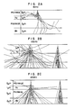
- FIG. 1 shows the cross-section of the X-ray mask.
- a membrane 524 made of material which is highly transmissible for the X-ray is overlaid by a pattern 525 made of material which is resistive against the transmission of X-ray, and in some cases the surface is coated with a thin film 526 for the purpose of protecting the pattern 525.
- the membrane is formed of a composed film made up of BN with a thickness of 2 ⁇ m and polyimide with a thickness of 3 ⁇ m, and the pattern is formed of Au with a thickness of 1 ⁇ m, which is coated with a polyimide protection film to complete an X-ray mask.
- Fig. 2 shows the result of a computer simulation, based on the Monte Carlo method, for the dispersion process of the electron beam in the X-ray mask. At an acceleration voltage of 30 kV, electrons are absorbed in the Au pattern, and the mask is expected to be charged. In fact, when the SEM was operated at an acceleration voltage of 30 kV, the X-ray mask was charged and the pattern could not be detected satisfactorily.
- the acceleration voltage being raised to 200 kV, the beam flares less in the protection film and the pattern can be detected at a higher resolution.
- an acceleration voltage of 75 kV or higher the X-ray mask is not charged and the pattern can be detected stably.
- Fig. 3 shows the distribution of dispersion angles of electrons in the pattern and membrane. Electrons are dispersed more prominently in the pattern layer than in the membrane.
- the following describes a method of well-contrast pattern detection which utilizes the difference in dispersion angle distribution between the pattern and membrane.
- the detector detects electrons having dispersion angles from O to ⁇ (will be termed "detection angle of ⁇ ")
- the detected signal has a value which is the integration of the dispersion distribution curve from O to ⁇ , i.e., the detected signal for the pattern is an area defined by the curve OB′A, line OA′ and line AA′
- the detected signal for the membrane is an area defined by the curve OBA, line OA′ and line AA′.
- the contrast is given as a difference between the detected signals for the membrane and pattern, i.e., an area defined by the curves OBA and OB′A.
- the next case is a detection angle of ⁇ .
- the detected signal for the membrane is an area defined by the curve OB, line OB ⁇ and line BB ⁇
- the detected signal for the pattern is an area defined by the curve OB′, line OB ⁇ and line BB ⁇
- the contrast is the difference of these signals, i.e., an area defined by the curve OB, curve OB ⁇ and line BB′. This area is smaller than that of the contrast for the detection angle ⁇ by the area defined by the line BB′, curve BA and curve B′A.
- the contrast of a detection angle ⁇ is smaller than that of the detection angle ⁇ .
- the contrast of a detection angle ⁇ is given as an area defined by the curve BA and curve OB′A subtracted by an area defined by the curve AC, curve AC′ and line CC′, and therefore it is smaller than the constant for the detection angle ⁇ . From the above discussion, it is concluded that the detection angle ⁇ provides the maximum contrast. Accordingly, the pattern can be detected at a satisfactory contrast by detecting electrons having dispersion angles from O to ⁇ .
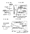
- FIGs. 4A to 4D show the distributions of dispersion angles in the pattern and membrane of X-ray masks, as an object to be tested, evaluated by the simulation of electron dispersion based on the Monte Calro method. The simulation was conducted for the case of an electron acceleration voltage of 200 kV for two kinds of X-ray masks.
- One X-ray mask is a composed film of a BN with a 2 ⁇ m thickness and polyimide with a thickness of 3 ⁇ m, and the pattern is formed of Au with a thickness of 2 ⁇ m.
- FIGs. 4A-4D reveal that the maximum contrast is obtained at a detection angle of about 0.2 rad, although it varies to some extent depending on the structure of X-ray mask. This value is incomparably larger than the detection angle of the conventional STEM.
- the detection angle ⁇ depends on the electron acceleration voltage, having a smaller value for a higher acceleration voltage and a larger value for a lower acceleration voltage. A proper value is in the range from 5° to 25°, approximately.
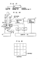
- Figs. 5A and 5B show the measured values which represent the relation between the contrast and the detection angle. Shown in Fig. 5B is a graph which is equivalent to the result of integration of Figs. 4A-4D.
- the contrast which is the difference between the substrate signal and pattern signal, has a maximum value at a detection angle of about 0.2 rad, according to the measurement, as expected by the simulation.
- Figs. 6A and 6B show an example of S/N ratio improvement based on different detection angles. It was confirmed that the present invention enhances the SN ratio by 10 fold or more as compared with the conventional case.
- the conventional electron beam detector has a detection clock frequency of about 4 MHz.
- detection can be speed up by using an electron multiplying tube, the sensitivity of detection for high-acceleration electrons is low, and it cannot be used for STEM.
- the sensitivity of detection can be raised.
- the inventive image restoration method and pattern external view inspection apparatus based on the scanning transmission electron microscope is intended to remover a deteriorated image with a dull waveform caused by the delay of response of the image detection system by modeling the transfer function of the image detection system and describing the model in the form of sum and product of first-order delay elements, and, since constituent elements of the electron beam detecting system including a scintillator, photoelectron multiplying tube and semiconductor detector, for example, can be approximated accurately in the form of a first-order delay element or the sum of first-order delay elements, by implementing the signal processing in accordance with the differential equation obtained through the inverse Laplace transformation of the inverse function of the transfer function, thereby recovering the deterioration of detected waveform.
- This signal processing results in increased noises in the image, and therefore a smoothing process is conducted in advance for the detected image thereby to suppress the increase of noises caused by the restoration of the detected waveform, and because most of noises in the detected image are created before the image detection system, they include less hgh-frequency components and therefore cannot be eliminated with a high-frequency cut filter, and to cope with this matter, by noticing the small amplitude of noises, a smoothing filter is activated when the variation of signal level in a local region is small or the original signal is delivered directly when the signal level varies greatly, as a smoothing process for the detected image, and by implementing the restoration process for the detected waveform following the smoothing process, a restored image including less noises is obtained.
- Scanning image detecting apparatus such as a laser scanning electron microscope, external view inspection apparatus and extraneous substance inspection apparatus, using the inventive point sensor imaging means operate to recover the deterioration of detected waveform in the same manner by obtaining in advance the transfer function of the image detecting system including a photodetector or photoelectron multiplying tube and by implementing a signal processing in accordance with the differential equation obtained by the laplace transformation of the inverse function of the transfer function. In eliminating noises in the detected signal, a smoothing process is conducted prior to the restoration process.
- a deteriorated image signal y(t) is rendered a Laplace transformation Y(s) for the transfer function G(s) of image detection system in terms of the Laplace transformation X(s) of the original image signal x(t) as follows.
- Y(s) G(s) ⁇ X(s) (1)
- 1/G(s) of G(s) the original image can be restored from the deteriorated image as follows.
- This restoration process is a computation on the Laplace transformation plane (Fourier transformation plane), and 1/G(s) is called an inverse filter.
- the restoration based on the inverse filter necessitates fourier transformation for the image, activation of the inverse filter, and inverse Fourier transformation for image restoration, and the volume of computation is too large to be suited for the real time processing.
- various filters such as a Wiener filter, all of which involve computations on the Fourier transformation plane, and therefore they require a large volume of computation.
- Another proposal is the image restoration based on the iteration method, but this successive approximation method imposes a large volume of computation, making the real time process difficult.
- the equation (2) is not generally rendered the analytical Laplace transformation, but it is made possible by expressing the G(s) in such a specific form as an integral element, differential element or first-order delay element.
- the transfer function of the whole electron beam detecting system becomes the sum and product of first-order delay elements.
- the G(s) is assumed to be a first-order delay element as follows.
- ⁇ is the time constant.
- the differential of this signal can be calculated as difference which requires a small volume of computation, and the real time process is possible.
- the restoration by the equation (4) includes the differentiation process, which increases noises, and it is effective for suppressing the increase of noise to perform a prior smoothing process for the deteriorated image.
- an averaging filter or center value filter is used to smooth the entire frame of the deteriorated image, effective signal components are also weakened along with noises, and it is not possible for the restoration process to restore a completely deterioration-free original image.
- a high-frequency cut filter cannot eliminate noises, since most of noises are created before the detection system and the noises have little high-frequency components.
- a smoothing filter is activated when the variation of signal level in a local region is small or the original signal is delivered directly when the signal level varies greatly, as an effective smoothing process.
- the restoration process which is represented by the equation (4) is conducted after the nonlinear smoothing process, a restored image including little noise can be obtained, and fast detection is made possible.
- the inventive pattern inspection apparatus comprises an electron gun 1, a convergent lens 2, an objective lens 3, a deflection coil 4, an object under test 5, a sample stage 6, a laser length meter 60, a scintillator 7, a light guide 8, a photoelectron multiplying tube 9, an amplifier 10, an A/D converter 11, a scanning signal generator 12, a deflection coil driver 13, a stage controller 14, a memory 15, a reading circuit 16, an image signal generator 17, a comparator 18, a defect judgement circuit 19, a focus detector 20, a brightness detector 21, an injection diagram 22, and a computer 23.
- An electron beam generated by the electron gun 1 is converged by the convergent lens 2 and objective lens 3 to form a spot on the object 5.
- the electron acceleration voltage is set sufficiently high so that the electron beam is transmitted through the object.
- the voltage is about 75 kV or higher.
- the electron beam 24 is deflected to scan the object 5 by means of the deflection coil 4 which is driven by the deflection coil driver 13 is accordance with the signal from the scanning signal generator 12.
- the scintillator 7 since the scintillator 7 also detects the X-rays, the diaphragm 22 is preferably made of material which produces less amount of X-rays be being excited by the electron beam, e.g., carbon. It is also possible to obtain the optimal detection angle by adjusting the detection area of the scintillator 7 or the distance between the object 5 and the scintillator 7.
- the diaphragm 22 is designed to be interchangeable to provide different diaphragm diameters, it is designed to be movable in the vertical direction, or it is designed to vary the diaphragm diameter, preferably.
- the electron beam is converted into the light by the scintillator 7, and it is led by the light guide 8 to the photoelectron multiplying tube 9, by which the light is converted into an electrical signal.
- the electron beam detector is not confined to the method of detection with the scintillator and electron multiplying tube, but it is also possible to use a semiconductor detector, for example.
- the electrical signal produced by the photoelectron multiplying tube 9 is amplified by the amplifier 10, synchronized with the scanning signal, and quantized by the A/D converter 11 to produce a scanning transmission electron image (STEM image).
- the design data which has been used to draw the pattern of the object is read out of the memory 15 by the reading circuit 16, and a reference image at the position of detection is produced by the image signal generator 17.
- the signal is entered to the comparison circuit 18 in synchronism with the STEM image.
- the reference image and STEM image are subjected to position matching, and inconsistent portions are delivered to the defect judgement circuit 19.
- the defect judgement circuit 19 discriminates as defects only inconsistent portions above the allowable level, among the detected inconsistent portions.
- the computer 23 issues a command to the stage control circuit 14 so that the sample stage 6 is fed by one step for the inspection of a new field. These operations are repeated until the entire surface of the object 5 is inspected.
- the sample stage 6 may be moved at a constant speed so that it is scanned at right angles with the moving direction by the electron beam 24 which is deflected by the deflection coil 4.
- Figs. 8A-8C show, as an example, the detection of only electrons with a specific dispersion angle by use of a plurality of electron beam detectors 27.
- An object under test 5 is fixed on the stage 6 by means of a chuck 25.
- the electron beam detectors 27 are mounted on the sample stage 6 in a matrix arrangement as shown in Fig. 8B. After being dispersed in the object 5, the electron beam 24 is detected by the electron beam detectors 27.
- the electron beam detectors 27 are semiconductor detectors, for example. By summing signals of specific detectors among the signals of all detectors, only electrons with a specific range of dispersion angle can be detected.
- the same effect as the injection diaphragm as has been explained on Fig. 7 is achieved.
- the detection angle can be kept constant invariably.
- the pattern contrast can be varied arbitrarily.
- Fig. 9 shows the structure of the objective lens and sample stage in the pattern detector intended for X-ray masks having diameters of 2 inches, 3 inches or more.
- the conventional STEM is based on the in-lens system, in which a sample is placed in the polepiece of lens, allowing merely the inspection of objects with sizes of several millimeters at the most.
- the inventive apparatus employs the out-lens system, in which a sample is placed outside of the magnetic path of the lens, with a large sample stage being disposed beneath the objective lens, thereby allowing the inspection of X-ray masks.
- the objective lens of the out-lens system is made up of a magnetic path 29 and a lens coil 30, with a stigma correction coil 28 being disposed inside the magnetic path 29.
- An X-ray mask 33 under test is encased in a mask holder 34 and held on the sample stage 6, which is movable in the X, Y, Z, ⁇ and tilt directions.
- the x-ray mask 33 is detachable against the sample stage 6 while it is accommodated in the mask holder 34.
- the electron beam 24 has its irradiation angle ⁇ determined by the object diaphragm 31, and it forms a specified spot diameter and beam current on the X-ray mask 33.
- an objective lens with a magnetic pole aperture diameter on the beam upstream side, magnetic pole spacing, and pole aperture diameter on the beam downstream side of 30 mm, 11 mm and 24 mm, respectively, produces a beam spot diameter of 40 mm and a beam current of 5 nA in the case of an irradiation angle (half angle) of 7 mrad.
- Making the irradiation angle ⁇ larger increases the beam current, resulting in an improved SN ratio, while at the same time the beam diameter increases unfavorably due to the aberration of the lens.
- a larger irradiation angle ⁇ for high S/N detection is much advantageous, whereas in order to detect small defects, a smaller irradiation angle ⁇ for small spot diameter is must advantageous.
- minimal defects to be detected is conceivably 0.07 to 0.1 mm, which requires a spot diameter of 0.1 ⁇ m or less.
- excessive reduction in the spot diameter not only results adversely in a degraded SN ratio, but also in an enlarged beam diameter on the pattern due to the dispersion of electrons on the polyamide protection film on the X-ray mask, and the resolution of detection is not improved. Accordingly, it is favorable to gain the beam current by setting the spot diameter alike a minimal defect to be detected or half that size.
- the objective lens in the magnetic path 29 has a planar bottom surface, and a sliding member 32 fixed to the mask holder 34 is pressed to the bottom surface of the magnetic path 29, thereby suppressing the mechanical vibration of the sample stage 6, and a stable detected image can be obtained.
- a possible method is to move the sample stage 6 while the sliding member 32 is pushed upward, or to lower the sliding member 32 for the movement of the sample stage 6 and push up at detection.
- the sliding member 32 is made of small-friction material, e.g., teflon, preferably.
- Another method is to fix the sliding member 32 to the upper surface of the sample stage 6 or the bottom surface of the objective lens in the magnetic path 29, instead of fixing it to the mask holder.
- Figs. 10A and 10B show the bonding section between the scintillator 7 and light guide 8 that are parts of the electron beam detector.
- Fig. 10A is the cross-sectional view and Fig. 10B in the plan view.
- a scintillator with a short afterglow time e.g., monocrystal of yttrium aluminum perovskite (YAP)
- YAP yttrium aluminum perovskite
- YAP has a high refraction factor of 1.96, and the scintillator irradiates much light from the side surface than from the bottom surface.
- a cylindrical light guide is cut as shown in Figs.
- the light guide 8 with the scintillator being bonded is coated with aluminum excluding the contact surface with the photoelectron multiplying tube 9, thereby preventing the scintillator from charging, and the light correcting efficiency of the scintillator is enhanced.
- the YAP radiation light is ultraviolet rays having a center wavelength of 380 nm
- a UV transmission filter 35 which cuts off the visual rays and transmits the ultraviolet rays, between the light guide 8 and photoelectron multiplying tube 9, the influence of stray light originating from the laser length measuring unit 60 which measures the position of the sample stage 6 can be prevented.
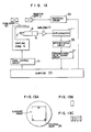
- Fig. 11 shows in block diagram the method of automatic focusing.
- Step 51 focus the electron beam on the entire surface of the X-ray mask, and thereafter step 52 detects patterns and step 53 moves the stage.
- the objective lens has a focal depth of 6 ⁇ m and the X-ray mask has a flatness of 1 ⁇ m, and therefore once the mask is focused the focus operation is not required any longer, provided that the sample stage is an ideal one. In reality, however, focusing needs to take place at a certain time interval in consideration of the parallelism of the sample stage and the stability of lens excitation current.
- step 54 is provided so that the pattern detection and stage movement are repeated for a certain period and then the automatic focusing is carried out at a certain interval, whereby patterns are always in focus for detection and the detection speed is not degraded since the focusing operation does not take place at each stage movement.
- Fig. 12 shows the auto-focusing mechanism
- Figs. 13A, 13B and 13C show an X-ray mask suitable for the automatic focusing
- Fig. 13A is a plan view showing the focusing mask position
- Figs. 13B and 13C are plan views showing shapes of the focusing mark.
- the detecting apparatus has a focal depth of 6 ⁇ m, as compared with a 1 ⁇ m flatness of the X-ray mask in its exposure area, and therefore by adjusting the parallelism of the X-ray mask 33 by means of the tilt mechanism of the sample stage 6, the entire exposure area is rendered in-focus.
- the X-ray mask 33 with three or more focusing marks being arranged as shown in Fig.
- a focusing mark is first detected, the detected waveform is differentiated by a differentiation circuit 36, differentiated waveforms of several lines are summed by a differentiated value adding circuit 37, the slope of the edge waveform of the focusing mark is measured, and the height of the sample stage is controlled so that the slope is steepest by the mountain climb method.
- the excitation circuit 38 may be controlled so as to control the focal distance of the objective lens.
- the sample stage 6 is moved to detect another focusing mark, and the tilt mechanism of the sample stage 6 is controlled so that the mark edge is steepest. In this manner, three focusing marks 39 on the X-ray mask are brought to in-focus, and consequently the entire exposure area is made in-focus.
- a rectangular mark as shown in Fig. 13B may be used. It is also possible to use a line-and-space mark as shown in Fig. 13C to implement focusing on the basis of the amplitude of detected waveform.
- Fig. 14 shows a method of correcting a drift of brightness of the detected image.
- step 54 repeats the pattern detection of step 52 and the stage movement of step 53 in a certain duration
- step 55 implements the brightness correction at a certain interval.
- Fig. 15 shows the brightness correcting mechanism.
- the detected signal provided by the photoelectron multiplying tube 9 is amplified and then quantized by the A/D converter 11, and the histogram of the detected image is measured by the brightness measuring unit 21.
- the histogram presents a double-peak distribution, indicating distinct brightnesses of the substrate and pattern.
- the brightness is corrected by controlling the supply voltage to the photoelectron multiplying tube 9 so that the peak brightness of the distribution is constant.
- Another control parameter, besides the supply voltage to the photoelectron multiplying tube 9, is the gain of the amplifier 10 or the intensity of the electron gun 1.
- Fig. 17 shows an electron beam detector which detects the electron beam by using an electron multiplying tube 41.
- the efficiency of secondary electron generation from the first-stage diode of the bute is too low to have a practical detection sensitivity.
- a deceleration material 40 for decelerating the electron beam is placed at the front of the electron multiplying tube 41 thereby to detect a lower-voltage electron beam, resulting in a higher efficiency of secondary electron generation of the diode and in an enhanced detection sensitivity.
- the deceleration material 40 is a material which produces less back scattering electrons, preferably carbon for example.
- Fig. 18 shows the structure of the STEM which performs dynamic focusing and dynamic stigma correction.
- the electron beam 24 is swung by the deflection coil 4 to scan the object under test 5, and when the deflection angle increases the spot diameter expands due to the aberration of the objective lens 3.
- an astigmatism correction coil 28 and moving focal point correction coil 42 are activated to correct the astigmatism and out-focus. Because of a high acceleration voltage of the electron beam 24, the astigmatism correction coil 28 and moving focal point correction coil 42 must be powerful, causing both coils to be high impedance, which makes fast correction difficult.
- the scanning field is divided into several sub-fields as shown in Fig.
- a scanning signal generator 12 is designed to generate a sawtooth wave which is biased with a d.c. component in correspondence to each sub-field, and a moving focal point correction driver 43 and astigmatism correction coil driver 44 are operated accordingly to produce correction values tailored to suit each sub-field.
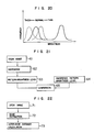
- Fig. 21 shows in block diagram a method of detecting the variation of pattern thickness across a wide range.
- Step 62 makes a histogram of the STEM image detected in step 61, as shown in Fig. 20, and step 63 evaluates the brightness level of the pattern.
- Step 65 compares the level obtained in step 63 with the reference brightness level which has been set in step 64 thereby to inspect the pattern thickness.
- Fig. 22 shows in block diagram a method of measuring the pattern dimensions by application of the inventive pattern detection apparatus.
- Step 72 detects the edge position of a pattern to be measured from the STEM image which has been detected in step 71.
- step 73 calculates the distance between the two edges, and the length measuring function is accomplished.
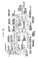
- Fig. 23 is a block diagram showing another embodiment of the pattern defect inspection apparatus using the inventive scanning electron microscope.
- Fig. 23 Shown in Fig. 23 is an X-ray mask pattern defect inspection apparatus using the scanning transmission electron microscope of Fig. 7, and identical components in these figures are referred to by the common symbols.
- Indicated by 74 is a synchronizing circuit, 75 is an electron detector, 76 is a smoothing circuit, 77 is a restoration circuit, 78 is a tone level conversion circuit, 791, 792, 793, 794 and 795 are binary threshold circuits, 801 and 802 are position deviation detecting circuits, 811 and 812 are image shift circuits 82 is a memory (of CAD data), 821 and 822 are pixel size conversion circuits 83 is a reading circuit, 831 and 832 are frame division circuits, 84 is an image signal generator, 85 is a corner rounding circuit, 86 is a multiple threshold circuit, 87 is an image comparison circuit, and 88 is a memory (of defects).
- the pattern defect inspection apparatus of this embodiment operates to compare an electron microscopic image of the X-ray mask pattern which is a sample 5 detected by the scanning transmission electron microscope shown in Fig. 7 with the ideal pattern produced from CAD data which is image data of the X-ray mask stored in the memory 82, and display inconsistent portions as defects.
- components including an electron gun 1, deflection coil 4, objective lens 3, electron beam detector 75, amplifier 10, deflection coil driver 13, synchronizing circuit 74, and A/D converter 11 are constituent elements of the usual scanning transmission electron microscope as have been explained on Fig. 7. Since the scanning transmission electron microscope has a view field which is narrower than the inspection area of the sample X-ray mask 5, the sample is placed on the stage 6 and the front face of the inspection area is inspected in step-and-repeat operation by a stage control circuit 14.
- the electron microscopic image provided by the restoration circuit 77 of the scanning transmission electron microscope is entered to the tone level conversion circuit 78 and the tone level is converted so that the average brightness of the pattern section and membrane section is equal to the reference value.
- the converted concentration value z′ of the image is evaluated by the following equation.
- the average concentration values p and m of the pattern section and membrane section are readily evaluated from the histogram of the detected image.
- the CAD data for drawing the pattern stored in the memory 82 is read out by the reading circuit 83, and a reference image (ideal image) of the mask pattern corresponding to the detection position of the sample 5 of the scanning transmission electron microscope is produced by the image signal generator 84.
- An actual mask pattern of the sample 5 has its corner rounded, and therefore the reference image produced by the image signal generator 84 is entered to the corner rounding circuit 85 for rounding so that a round corner of the mask pattern is not detected as a defect.
- a binary image is converted into a tone image by the multiple threshold circuit 86. This conversion process is conducted favorably by using a smoothing filter having a Gauss distribution for the point spread function PSF.
- the detected image provided by the tone conversion circuit 78 and the reference image provided by the multiple threshold circuit 86 are reformed into binary images by the binary threshold circuits 791 and 792, respectively, the positional deviation of the two images is calculated by the position deviation detection circuit 801, and the detected image is positioned by the image shift circuit 811.
- the pixel size is halved (e.g., from 0.05 ⁇ m/pix to 0.025 ⁇ m/pix) by the pixel size conversion circuits 821 and 822. This conversion process divides a pixel into four pixels, and the processing equations are as follows.
- A, B, C, and D are brightness of pixels before conversion
- a, b, c and d are brightnesses of pixels after conversion. Because of the presence of image distortion included in a detected image of the scanning transmission electron microscope, positioning is conducted once again. If there is a pixel distortion, positioning for the entire frame merely results in an average positioning for the whole. Since each section of a frame can further be positioned individually, a frame is divided and each divisional frame is rendered positioning through a further binary reformation.
- the frame dividing circuits 831 and 832 implement frame division for the detected image and reference image, the binary threshold circuits 793 and 794 reform the images into binary, and the positioning deviation circuit 802 evaluates the position deviation of frames of the two images, and the image shift circuit 812 positions the frame of the detected image.
- the image comparison circuit 87 performs tone image comparison for the detected image and reference image which have been positioned as described above, and the binary threshold circuit 795 reforms the differential image into binary, and coordinates of inconsistent portions are stored as defects in the memory 88.
- the algorism of tone image comparison by the image comparison circuit 87 is preferably the local perturbation pattern matching method.
- the local perturbation pattern matching method is an algorism which makes matching for the detected image to the reference image for each local region on the xy plane in the direction of brightness, and extracts unmatched portions as defects.
- the resulting tone image D(x, y) is given in terms of the differential image S k (x, y), detected image I(x, y) and reference image R(x, y) as follows.
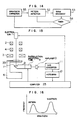
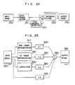
- Fig. 24 is a functional block diagram which represents the operational procedure of the smoothing circuit 76 shown in Fig. 23.
- indicated by 200 is an input image
- 210 is a local region slice circuit
- 220 is a level variation detecting circuit
- 230 is an averaging filter
- 240 is an output image.
- the output signal of the A/D converter 11 is fed to the local region slice circuit 210, which slices a local region of 3-by-3 pixels from the input image 200.
- the signal level variation within the local region is detected by the level variation detector 220, which then calculates a difference between the brightest concentration value and darkest concentration value within the local region.
- the concentration difference is smaller than a certain predetermined value, the signal levels within the local region are smoothed by the averaging filter 230, and if the concentration difference is larger than a certain predetermined value, the concentration (signal level) of the input image 200 is outputted directly, and output image 240 which is smoothed in a nonlinear fashion is obtained.
- the averaging filter 230 may be other filter, e.g., center value filter, provided that it has a smoothing ability.
- A max ⁇ in(i-1, j-1), in(i-1, j), in(i-1, j+1), in(i, j-1), in(i, j), in(i, j+1), in(i+1, j-1), in(i+1, j), in(i+1, j+1) ⁇
- Fig. 25 is a functional block diagram which presents the operational procedure of the restoration circuit 77 shown in Fig. 23.
- 300 is an input signal
- 310 is a second-order differentiation circuit
- 320 is a first-order differentiation circuit
- 330 is a convolution circuit
- 340, 350, 360 and 370 are multipliers
- 380 is an adder
- 390 is an output signal.
- the output signal of the smoothing circuit 76 shown in Fig. 23 is entered as the input signal 300 to the restoration circuit 77 of Fig.
- the quadratic differential of the input signal 300 is calculated by the quadratic differentiation circuit 310
- the primary differential of the input signal 300 is calculated by the first-order differentiation circuit 320
- the convolution of the input signal 300 is calculated by the convolution circuit 330
- the quadratic differential is multiplied by k1 by the multiplier 340
- the primary differential is multiplied by k2 by the multiplier 350
- the convolution is multiplied by k4 by the multiplier 360
- the input signal 300 is multiplied by k3 by the multiplier 370
- these four signals are summed by the adder 380 to obtain the output signal 390 as follows.
- I(s) ⁇ A2 ⁇ 1 ⁇ 2+(1-A1-A2) ⁇ 2 ⁇ 3+A1 ⁇ 3 ⁇ 1 ⁇ s2 + ⁇ (A1+A2) ⁇ 1+(1-A1) ⁇ 2+(1-A2) ⁇ 3 ⁇ s+1
- Equation (13) is the wanted restoration equation. Reforming differentiation to difference and integration to product-sum in the equation (13) for reducing the equation to the discrete type results as follows.
- the sampling frequency is set to 15 MHz, i.e., the sampling interval ⁇ t is set to 0.067 ⁇ s.
- Fig. 26 is a graph of the function h(t) of the equation (13′) in the restoration equation (13) of the restoration circuit 77 shown in Fig. 25, in which h(t) is plotted on the vertical axis against time t ( ⁇ s) on the horizontal axis.
- the function h(t) approaches zero as the value of t increases, and therefore the h(t) can be approximated to zero for t above a certain value.
- the convolution of the fourth term of the restoration equation (13) can have a limited period of integration.
- the equation (14) can further be reformed as follows.
- the equation can further be simplified by neglecting the term of convolution as follows.
- the restoration circuit 77 in Fig. 25 operates to receive the output signal y(t) of the smoothing circuit 76 as the input signal 300, calculate the quadratic differential of the signal y(t) based on the first term of the equation (15) using the second-order differentiation circuit 310, calculate the primary differential of the signal y(t) based on the second term of the equation (15) using the first-order differentiation circuit 320, calculate the convolution of the signal y(t) as the third term of the equation (15): using the convolution circuit 330, multiply the output of the second-order differentiation circuit 310 by k1 using the multiplier 340, multiply the output of the first-order differentiation circuit 320 by k2 using the multiplier 350, multiply the output of the convolution circuit 330 by multiply the signal y(t) by k3 using the multiplier 370, and sum these four signals using the adder 380 thereby to obtain the restored signal x(t) of the equation (15) as the output signal 390.
- Fig. 27 is a graph showing the deteriorated waveform y(t) of the input signal 300 and the restored waveform x(t) of the output signal 390 for a step response of the restoration circuit 77 shown in Fig. 25.
- the deteriorated waveform y(t) is fairly restored in the restored waveform x(t) on the basis of the restoration equations (15) and (16).
- the signal x(t) restored by the restoration circuit 77 is subjected to D/A conversion by the display circuit and it is displayed on a Braun tube.
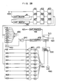
- Fig. 28 shows an example of the smoothing circuit 76 shown in Fig. 23 (Fig. 24).
- Fig. 28 indicated by 400 is an input terminal, 411 and 412 are shift registers, 421-429 are registers, 430 is an adder, 440 is a divider, 450 is a subtracter 470 is an absolute value calculator 480 is an adder, 490 is a memory, 500 is a comparator, 510 is a switch, and 520 is an output terminal. These components are connected as shown in the figure. From the input signal received from the A/D converter 11 on the input terminal 400 of Fig. 28, a local region of 3-by-3 pixels is sliced using the shift registers 411, 412, 421 and 429.
- the signal level variation is estimated as a difference between the maximum value and minimum value within a local region, here, it is estimated as a variance ⁇ ′ as follows. From the outputs of the registers 421-429 and the output y of the divider 440, the variance ⁇ ′ of equation (17) is calculated using the subtracter 460, absolute value calculator 470 and adder 480. The variance ⁇ ′ is compared with a predetermined constant K2 stored in the memory 490 using the comparator 550.
- the switch 510 In response to a comparison result of ⁇ ′ > K2, the switch 510 is set so that the contents of the register 425 are delivered directly to the output terminal 520 through a shift register 491, and in response to a comparison result of ⁇ ′ ⁇ K2, the mean value the mean value y of the local region from the divider 440 is delivered to the output terminal 520 through the switch 510 through a shift register 491.
- the shift registers 491 and 492 are used for timing the output of the comparator 500 with the output of the register 425 or the output of the divider 440.
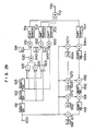
- Fig. 29 shows an example of the restoration circuit 77 shown in Fig. 23 (Fig. 25).
- Fig. 29 indicated by 600 is an input terminal, 611-613 are registers, 621-623 are subtracters 630 is an adder, 641-643 are memories, 651-653 are multipliers, 661-66m are memories, 671-67m are multipliers, 681-68m-1 are adders, 701-704 are shift registers, 710 is an adder, and 720 is an output terminal.
- the restoration circuit 77 of Fig. 29 is reformed for the above restoration equation (15) in terms of a signal string as follows.
- the circuit performs the restoring process based on the restoration equation (18).
- the restoration circuit 77 receives on its input terminal 600 the signal y(i) from the smoothing circuit 12, and stores the signals y(i+1), y(i) and y(i-1) in the resisters 611-613.
- the subtracters 621 and 622 and adder 630 operate to calculate the first term y(i+1)-2y(i)+y(i-1) of the equation (18) and the multiplier 651 multiplies it with a constant A1 stored in the memory 641, and the first term A1(y(i+1)-2y(i)+y(i-1)) is obtained.
- the circuit for calculating the fourth term of convolution of the input signal y(i) comprises memories 661-66m, multipliers 671-67m, registers 681-68m-1 and adders 691-69m-1.
- the outputs of the multipliers 651-653 and adder 69m-1 are timed by the shift registers 701-704 and summed by the adder 710, and the restored signal x(i) of the restoration equation (18) is produced on the output terminal 720.
- Fig. 30 is a block diagram showing a further embodiment of the pattern inspection apparatus using the inventive scanning transmission electron microscope. Shown in Fig. 30 is a further embodiment of the X-ray mask pattern inspection apparatus using the scanning transmission electron microscope of Fig. 7. Portions equivalent to those in Fig. 23 are referred to by the common symbols. Indicated by 89 is a response characteristics adding circuit.
- the pattern inspection apparatus of this embodiment differs from the embodiment of Fig. 23 in that the apparatus of Fig. 23 performs restoration of a detected image of the scanning transmission electron microscope using the smoothing circuit 76 and restoration circuit 77, whereas the apparatus of Fig.
- the response characteristics adding circuit 89 appends the response characteristics of the electron beam detection system of the scanning transmission electron microscope to a reference image (ideal image) generated from CAD data stored in the memory 82.
- the response characteristics adding circuit 89 dulls the waveform of the reference image in accordance with the transfer function G(s) of response characteristics of the electron beam detection system including the electron beam detector 75, amplifier 10 and A/D converter 11.
- the inverse Laplace transformation of this transfer function G(s), i.e., the impulse response g(t) is given as follows.
- the output signal y(t) is expressed as convolution in terms of the input signal x(t) and impulse response g(t) as follows.
- the response characteristics adding circuit 89 is designed to implement the equation (21), and it can be, for example, a digital signal processor DSP which calculates the convolution sum, or the circuit shown in Fig. 31. The rest is the same as Fig. 23.
- Fig. 31 shows the circuit for calculating the convolution sum of the response characteristics adding circuit 89 in Fig. 30.
- indicated by 1010 is an input terminal
- 1021-102 n are memories
- 1031-103 n are multipliers
- 1041-104 n-1 are registers
- 1051-105 n-1 are adders
- 1060 is an output terminal.
Landscapes
- Chemical & Material Sciences (AREA)
- Analytical Chemistry (AREA)
- Physics & Mathematics (AREA)
- General Physics & Mathematics (AREA)
- Length-Measuring Devices Using Wave Or Particle Radiation (AREA)
- Analysing Materials By The Use Of Radiation (AREA)
- Exposure Of Semiconductors, Excluding Electron Or Ion Beam Exposure (AREA)
- Testing Or Measuring Of Semiconductors Or The Like (AREA)
Applications Claiming Priority (2)
| Application Number | Priority Date | Filing Date | Title |
|---|---|---|---|
| JP162527/88 | 1988-07-01 | ||
| JP63162527A JP2602287B2 (ja) | 1988-07-01 | 1988-07-01 | X線マスクの欠陥検査方法及びその装置 |
Publications (2)
| Publication Number | Publication Date |
|---|---|
| EP0348992A2 true EP0348992A2 (de) | 1990-01-03 |
| EP0348992A3 EP0348992A3 (de) | 1991-07-31 |
Family
ID=15756309
Family Applications (1)
| Application Number | Title | Priority Date | Filing Date |
|---|---|---|---|
| EP19890111920 Withdrawn EP0348992A3 (de) | 1988-07-01 | 1989-06-30 | Gerät und Verfahren zum Nachweis von Mustern, die auf einem Transmissions-Rasterelektronenmikroskop basiert sind |
Country Status (3)
| Country | Link |
|---|---|
| US (1) | US5051585A (de) |
| EP (1) | EP0348992A3 (de) |
| JP (1) | JP2602287B2 (de) |
Cited By (6)
| Publication number | Priority date | Publication date | Assignee | Title |
|---|---|---|---|---|
| EP0513776A3 (de) * | 1991-05-15 | 1994-02-16 | Hitachi Ltd | |
| US5866905A (en) * | 1991-05-15 | 1999-02-02 | Hitachi, Ltd. | Electron microscope |
| WO2000039836A1 (en) * | 1998-12-29 | 2000-07-06 | Philips Electron Optics B.V. | Sem for transmission operation with a location-sensitive detector |
| WO2002075246A1 (en) * | 2001-03-16 | 2002-09-26 | Hitachi, Ltd. | Method for measuring dimensions of pattern |
| EP1455378A4 (de) * | 2001-11-21 | 2011-01-26 | Hitachi High Tech Corp | Probenabbildungsverfahren und system mit einem strahl geladener teilchen |
| TWI849016B (zh) * | 2018-12-14 | 2024-07-21 | 美商科磊股份有限公司 | 用於減小電子束量測中之系統誤差之方法及系統以及其相關之非暫時性電腦可讀儲存媒體 |
Families Citing this family (55)
| Publication number | Priority date | Publication date | Assignee | Title |
|---|---|---|---|---|
| JPS58110577A (ja) * | 1981-12-25 | 1983-07-01 | Nippon Soda Co Ltd | 光学活性な複素環化合物及び殺ダニ剤 |
| NL9100076A (nl) * | 1991-01-17 | 1992-08-17 | Philips Nv | Methode voor automatische uitlijning van een elektronenmicroscoop en een elektronenmicroscoop geschikt voor uitvoering van een dergelijke methode. |
| JP3148353B2 (ja) * | 1991-05-30 | 2001-03-19 | ケーエルエー・インストルメンツ・コーポレーション | 電子ビーム検査方法とそのシステム |
| JPH06135020A (ja) * | 1992-09-30 | 1994-05-17 | Citizen Watch Co Ltd | シリアルドットプリンタ装置 |
| JP2823450B2 (ja) * | 1992-11-19 | 1998-11-11 | 株式会社東芝 | 回路パターンの寸法測定方法 |
| JP2802571B2 (ja) * | 1993-03-23 | 1998-09-24 | 株式会社日立製作所 | 電子線測長装置 |
| US5406832A (en) * | 1993-07-02 | 1995-04-18 | Topometrix Corporation | Synchronous sampling scanning force microscope |
| DE4447593C2 (de) * | 1994-10-05 | 2000-12-07 | Clariant Gmbh | Toner für elektrophotographische Entwickler, enthaltend ein Azogelbpigment |
| JP3304681B2 (ja) * | 1995-04-25 | 2002-07-22 | 株式会社日立製作所 | 電子顕微鏡及び3次元原子配列観察方法 |
| IT1281384B1 (it) * | 1995-10-10 | 1998-02-18 | Finmeccanica Spa | Sistema per il confronto di immagini digitali. |
| US6159649A (en) * | 1996-06-13 | 2000-12-12 | Clariant Gmbh | Electrophotographic, resin-containing, electret, or inkjet compositions containing magenta azo pigment and use thereof |
| JP3490597B2 (ja) * | 1997-01-07 | 2004-01-26 | 株式会社東芝 | マスク検査装置 |
| US5998790A (en) * | 1997-06-18 | 1999-12-07 | The Regents Of The University Of California | Transmission electron microscope CCD camera |
| US5859429A (en) * | 1997-08-20 | 1999-01-12 | Abbott Laboratories | Optical system with test/calibration |
| JP3687541B2 (ja) * | 1999-01-04 | 2005-08-24 | 株式会社日立製作所 | 元素マッピング装置、走査透過型電子顕微鏡および元素マッピング方法 |
| WO2004105077A1 (ja) * | 1999-02-24 | 2004-12-02 | Katsuto Goto | 高密度記録走査顕微鏡 |
| JP2000314710A (ja) | 1999-04-28 | 2000-11-14 | Hitachi Ltd | 回路パターンの検査方法及び検査装置 |
| JP4069545B2 (ja) * | 1999-05-19 | 2008-04-02 | 株式会社日立製作所 | 電子顕微方法及びそれを用いた電子顕微鏡並び生体試料検査方法及び生体検査装置 |
| DE19927835A1 (de) | 1999-06-18 | 2000-12-21 | Clariant Gmbh | Verwendung von verbesserten Cyanpigmenten in elektrophotographischen Tonern und Entwicklern, Pulverlacken und Ink-Jet-Tinten |
| US7817844B2 (en) * | 1999-08-26 | 2010-10-19 | Nanogeometry Research Inc. | Pattern inspection apparatus and method |
| US7796801B2 (en) * | 1999-08-26 | 2010-09-14 | Nanogeometry Research Inc. | Pattern inspection apparatus and method |
| JP3360666B2 (ja) * | 1999-11-12 | 2002-12-24 | 日本電気株式会社 | 描画パターン検証方法 |
| DE19957245A1 (de) | 1999-11-27 | 2001-05-31 | Clariant Gmbh | Verwendung von salzartigen Struktursilikaten als Ladungssteuermittel |
| JP2001153637A (ja) * | 1999-11-29 | 2001-06-08 | Nec Corp | マスク検査装置及び検査方法 |
| US6633174B1 (en) * | 1999-12-14 | 2003-10-14 | Kla-Tencor | Stepper type test structures and methods for inspection of semiconductor integrated circuits |
| US6459089B1 (en) * | 2000-03-03 | 2002-10-01 | Steris Inc. | Single accelerator/two-treatment vault system |
| US6862142B2 (en) * | 2000-03-10 | 2005-03-01 | Kla-Tencor Technologies Corporation | Multi-detector microscopic inspection system |
| US7655482B2 (en) * | 2000-04-18 | 2010-02-02 | Kla-Tencor | Chemical mechanical polishing test structures and methods for inspecting the same |
| DE10054344A1 (de) | 2000-11-02 | 2002-05-29 | Clariant Gmbh | Verwendung von gecoateten Pigmentgranulaten in elektrophotographischen Tonern und Entwicklern, Pulverlacken und Ink-Jet-Tinten |
| JP4667650B2 (ja) * | 2001-06-08 | 2011-04-13 | エスアイアイ・ナノテクノロジー株式会社 | 断面観察方法及び集束イオンビーム装置 |
| JP3944439B2 (ja) * | 2002-09-26 | 2007-07-11 | 株式会社日立ハイテクノロジーズ | 電子線を用いた検査方法および検査装置 |
| JP4187544B2 (ja) * | 2003-02-25 | 2008-11-26 | 富士通株式会社 | 走査透過型電子顕微鏡 |
| JP4185789B2 (ja) * | 2003-03-12 | 2008-11-26 | 株式会社日立ハイテクノロジーズ | パターン検査方法及びその装置 |
| JP4647977B2 (ja) * | 2004-11-30 | 2011-03-09 | 日本電子株式会社 | Fib自動加工時のドリフト補正方法及び装置 |
| JP4734135B2 (ja) * | 2005-10-19 | 2011-07-27 | 株式会社日立ハイテクノロジーズ | 荷電粒子線装置、それに用いられるコンピュータプログラム、及び試料像観察方法 |
| JP4822826B2 (ja) * | 2005-12-06 | 2011-11-24 | 日本電子株式会社 | 粒子解析方法及び装置 |
| JP4985352B2 (ja) | 2007-11-28 | 2012-07-25 | 株式会社島津製作所 | 放射線検出器 |
| JP5174498B2 (ja) * | 2008-03-19 | 2013-04-03 | 株式会社日立ハイテクノロジーズ | 荷電粒子ビーム装置 |
| US7943889B2 (en) * | 2008-03-21 | 2011-05-17 | Prairie Technologies, Inc. | Apparatus for improving detection efficiency of multiphoton microscopy systems by focus compensation, pupil image division, and parallel pupil rearrangement |
| JP5649583B2 (ja) * | 2008-10-31 | 2015-01-07 | エフ イー アイ カンパニFei Company | 加工終点検出方法及び装置 |
| US8125518B2 (en) * | 2008-12-15 | 2012-02-28 | Hitachi High-Technologies Corporation | Scanning electron microscope |
| US8150140B2 (en) * | 2008-12-22 | 2012-04-03 | Ngr Inc. | System and method for a semiconductor lithographic process control using statistical information in defect identification |
| JP5429869B2 (ja) * | 2008-12-22 | 2014-02-26 | 株式会社 Ngr | パターン検査装置および方法 |
| JP5502407B2 (ja) * | 2009-09-17 | 2014-05-28 | 日本電子株式会社 | 共焦点stem像取得方法及び装置 |
| JP5216739B2 (ja) * | 2009-10-15 | 2013-06-19 | 株式会社日立ハイテクノロジーズ | 荷電粒子線装置、及び膜厚測定方法 |
| JP5386453B2 (ja) * | 2010-08-24 | 2014-01-15 | 株式会社日立ハイテクノロジーズ | 荷電粒子線装置および試料観察方法 |
| JP2015164091A (ja) * | 2012-05-11 | 2015-09-10 | 株式会社日立ハイテクノロジーズ | 電子顕微鏡 |
| JP5936484B2 (ja) * | 2012-08-20 | 2016-06-22 | 株式会社日立ハイテクノロジーズ | 荷電粒子線装置及び試料観察方法 |
| DE112014002043T5 (de) * | 2013-05-30 | 2016-01-14 | Hitachi High-Technologies Corporation | Mit einem Strahl geladener Teilchen arbeitende Vorrichtung und Probenbeobachtungsverfahren |
| WO2016149676A1 (en) | 2015-03-18 | 2016-09-22 | Battelle Memorial Institute | Electron beam masks for compressive sensors |
| US10170274B2 (en) * | 2015-03-18 | 2019-01-01 | Battelle Memorial Institute | TEM phase contrast imaging with image plane phase grating |
| WO2017189212A1 (en) | 2016-04-29 | 2017-11-02 | Battelle Memorial Institute | Compressive scanning spectroscopy |
| JP6718782B2 (ja) * | 2016-09-21 | 2020-07-08 | 日本電子株式会社 | 対物レンズおよび透過電子顕微鏡 |
| US10295677B2 (en) | 2017-05-08 | 2019-05-21 | Battelle Memorial Institute | Systems and methods for data storage and retrieval |
| JP6796616B2 (ja) * | 2018-05-24 | 2020-12-09 | 日本電子株式会社 | 荷電粒子線装置および画像取得方法 |
Family Cites Families (19)
| Publication number | Priority date | Publication date | Assignee | Title |
|---|---|---|---|---|
| US3626184A (en) * | 1970-03-05 | 1971-12-07 | Atomic Energy Commission | Detector system for a scanning electron microscope |
| JPS5131146B2 (de) * | 1971-11-12 | 1976-09-04 | ||
| US4068123A (en) * | 1973-07-27 | 1978-01-10 | Nihon Denshi Kabushiki Kaisha | Scanning electron microscope |
| JPS5093078A (de) * | 1973-12-17 | 1975-07-24 | ||
| JPS5741062B2 (de) * | 1974-03-01 | 1982-09-01 | ||
| US3987242A (en) * | 1974-04-24 | 1976-10-19 | American Optical Corporation | Automatic dc restorer and gain control |
| DE2529735C3 (de) * | 1975-07-01 | 1978-06-08 | Max-Planck-Gesellschaft Zur Foerderung Der Wissenschaften E.V., 3400 Goettingen | Korpuskularstrahlmikroskop, insbe- · sondere Elektronenmikroskop, mit Verstelleinrichtungen zur Änderung der Lage des abzubildenden Objekts und Verfahren zum Betrieb |
| DE2619739A1 (de) * | 1976-04-30 | 1977-11-10 | Max Planck Gesellschaft | Durchstrahlungs-raster-korpuskularstrahlmikroskop mit unterteiltem detektor im primaerstrahlkegel |
| JPS5481075A (en) * | 1977-11-24 | 1979-06-28 | Cho Lsi Gijutsu Kenkyu Kumiai | Method of detecting article image using electron beam |
| US4366380A (en) * | 1979-10-11 | 1982-12-28 | George Mirkin | Method and apparatus for structural analysis |
| JPS56135152U (de) * | 1980-03-13 | 1981-10-13 | ||
| FR2520177B1 (fr) * | 1982-01-15 | 1986-05-23 | Pierre Jutier | Dispositif de saisie et de restitution en temps reel d'une image formee de trames successives de lignes de balayage |
| US4602282A (en) * | 1982-06-29 | 1986-07-22 | Hamamatsu Photonics Kabushiki Kaisha | Measuring devices for two-dimensional photon-caused or corpuscular-ray-caused image signals |
| JPS5919318A (ja) * | 1982-07-23 | 1984-01-31 | Hitachi Ltd | 転写パタ−ンの位置ずれ検査方法および転写パタ−ンマスク |
| JPS616253U (ja) * | 1984-06-19 | 1986-01-14 | 日本電子株式会社 | 電子顕微鏡における検出器 |
| DE3500903A1 (de) * | 1985-01-12 | 1986-07-17 | Fa. Carl Zeiss, 7920 Heidenheim | Detektor fuer rueckstreuelektronen |
| JPS62237307A (ja) * | 1986-04-09 | 1987-10-17 | Toshiba Corp | 寸法測定装置 |
| JPS62260335A (ja) * | 1986-05-06 | 1987-11-12 | Hitachi Ltd | パタ−ン検査方法および装置 |
| JPH01102841A (ja) * | 1987-10-14 | 1989-04-20 | Toshiba Corp | 画像形成方法 |
-
1988
- 1988-07-01 JP JP63162527A patent/JP2602287B2/ja not_active Expired - Fee Related
-
1989
- 1989-06-28 US US07/373,223 patent/US5051585A/en not_active Expired - Lifetime
- 1989-06-30 EP EP19890111920 patent/EP0348992A3/de not_active Withdrawn
Cited By (8)
| Publication number | Priority date | Publication date | Assignee | Title |
|---|---|---|---|---|
| EP0513776A3 (de) * | 1991-05-15 | 1994-02-16 | Hitachi Ltd | |
| US5475218A (en) * | 1991-05-15 | 1995-12-12 | Hitachi, Ltd. | Instrument and method for 3-dimensional atomic arrangement observation |
| US5866905A (en) * | 1991-05-15 | 1999-02-02 | Hitachi, Ltd. | Electron microscope |
| WO2000039836A1 (en) * | 1998-12-29 | 2000-07-06 | Philips Electron Optics B.V. | Sem for transmission operation with a location-sensitive detector |
| US6376839B1 (en) | 1998-12-29 | 2002-04-23 | Philips Electron Optics | SEM for transmission operation with a location-sensitive detector |
| WO2002075246A1 (en) * | 2001-03-16 | 2002-09-26 | Hitachi, Ltd. | Method for measuring dimensions of pattern |
| EP1455378A4 (de) * | 2001-11-21 | 2011-01-26 | Hitachi High Tech Corp | Probenabbildungsverfahren und system mit einem strahl geladener teilchen |
| TWI849016B (zh) * | 2018-12-14 | 2024-07-21 | 美商科磊股份有限公司 | 用於減小電子束量測中之系統誤差之方法及系統以及其相關之非暫時性電腦可讀儲存媒體 |
Also Published As
| Publication number | Publication date |
|---|---|
| EP0348992A3 (de) | 1991-07-31 |
| JP2602287B2 (ja) | 1997-04-23 |
| JPH0215545A (ja) | 1990-01-19 |
| US5051585A (en) | 1991-09-24 |
Similar Documents
| Publication | Publication Date | Title |
|---|---|---|
| EP0348992A2 (de) | Gerät und Verfahren zum Nachweis von Mustern, die auf einem Transmissions-Rasterelektronenmikroskop basiert sind | |
| JP5937171B2 (ja) | 走査型電子顕微鏡及び試料観察方法 | |
| US4814615A (en) | Method and apparatus for detecting defect in circuit pattern of a mask for X-ray exposure | |
| US20110187847A1 (en) | Scanning type charged particle microscope device and method for processing image acquired with scanning type charged particle microscope device | |
| US8993961B2 (en) | Electric charged particle beam microscope and electric charged particle beam microscopy | |
| US6627884B2 (en) | Simultaneous flooding and inspection for charge control in an electron beam inspection machine | |
| US4169244A (en) | Electron probe testing, analysis and fault diagnosis in electronic circuits | |
| JP3424512B2 (ja) | 粒子ビーム検査装置および検査方法並びに粒子ビーム応用装置 | |
| JP2005310602A (ja) | 荷電粒子線調整方法、及び荷電粒子線装置 | |
| JP2003303568A (ja) | 電子顕微鏡のチャージアップ防止方法および電子顕微鏡 | |
| JP2009043936A (ja) | 電子顕微鏡 | |
| US7154090B2 (en) | Method for controlling charged particle beam, and charged particle beam apparatus | |
| US9110384B2 (en) | Scanning electron microscope | |
| KR102936423B1 (ko) | 학습기의 학습 방법 및 화상 생성 시스템 | |
| GB1594597A (en) | Electron probe testing analysis and fault diagnosis in electronic circuits | |
| US3909610A (en) | Apparatus for displaying the energy distribution of a charged particle beam | |
| EP0050475B1 (de) | Gerät zur Abtastbilderzeugung mit Hilfe photoelektrischer Signale | |
| TWI843354B (zh) | 帶電粒子線裝置及使用其之檢查方法 | |
| US5086227A (en) | Secondary ion mass analyzing apparatus | |
| US4804840A (en) | Apparatus for detecting focused condition of charged particle beam | |
| JP2002216698A (ja) | ウエハの欠陥検査装置及び該装置を用いたデバイス製造方法 | |
| JP4431624B2 (ja) | 荷電粒子線調整方法、及び荷電粒子線装置 | |
| JP2010016007A (ja) | 荷電粒子線調整方法及び荷電粒子線装置 | |
| Donders et al. | An improved optical system for photofield emission | |
| JPH11224642A (ja) | 電子ビーム露光装置および電子ビーム露光方法 |
Legal Events
| Date | Code | Title | Description |
|---|---|---|---|
| PUAI | Public reference made under article 153(3) epc to a published international application that has entered the european phase |
Free format text: ORIGINAL CODE: 0009012 |
|
| AK | Designated contracting states |
Kind code of ref document: A2 Designated state(s): DE FR GB |
|
| 17P | Request for examination filed |
Effective date: 19901120 |
|
| PUAL | Search report despatched |
Free format text: ORIGINAL CODE: 0009013 |
|
| AK | Designated contracting states |
Kind code of ref document: A3 Designated state(s): DE FR GB |
|
| STAA | Information on the status of an ep patent application or granted ep patent |
Free format text: STATUS: THE APPLICATION HAS BEEN WITHDRAWN |
|
| 18W | Application withdrawn |
Withdrawal date: 19930118 |