EP0239736B2 - Langgestreckte Gestelle und zugehörige Teile zum lösbaren Befestigen von zu galvanisierenden Leiterplatten, sowie zugehörige Leiterplatten - Google Patents
Langgestreckte Gestelle und zugehörige Teile zum lösbaren Befestigen von zu galvanisierenden Leiterplatten, sowie zugehörige Leiterplatten Download PDFInfo
- Publication number
- EP0239736B2 EP0239736B2 EP87101190A EP87101190A EP0239736B2 EP 0239736 B2 EP0239736 B2 EP 0239736B2 EP 87101190 A EP87101190 A EP 87101190A EP 87101190 A EP87101190 A EP 87101190A EP 0239736 B2 EP0239736 B2 EP 0239736B2
- Authority
- EP
- European Patent Office
- Prior art keywords
- racks
- accordance
- springs
- printed circuit
- circuit boards
- Prior art date
- Legal status (The legal status is an assumption and is not a legal conclusion. Google has not performed a legal analysis and makes no representation as to the accuracy of the status listed.)
- Expired - Lifetime
Links
Images

Classifications
-
- C—CHEMISTRY; METALLURGY
- C25—ELECTROLYTIC OR ELECTROPHORETIC PROCESSES; APPARATUS THEREFOR
- C25D—PROCESSES FOR THE ELECTROLYTIC OR ELECTROPHORETIC PRODUCTION OF COATINGS; ELECTROFORMING; APPARATUS THEREFOR
- C25D17/00—Constructional parts, or assemblies thereof, of cells for electrolytic coating
- C25D17/06—Suspending or supporting devices for articles to be coated
- C25D17/08—Supporting racks, i.e. not for suspending
-
- H—ELECTRICITY
- H05—ELECTRIC TECHNIQUES NOT OTHERWISE PROVIDED FOR
- H05K—PRINTED CIRCUITS; CASINGS OR CONSTRUCTIONAL DETAILS OF ELECTRIC APPARATUS; MANUFACTURE OF ASSEMBLAGES OF ELECTRICAL COMPONENTS
- H05K3/00—Apparatus or processes for manufacturing printed circuits
- H05K3/22—Secondary treatment of printed circuits
- H05K3/24—Reinforcing the conductive pattern
- H05K3/241—Reinforcing the conductive pattern characterised by the electroplating method; means therefor, e.g. baths or apparatus
Definitions
- the invention relates to elongated frames and associated parts for the detachable fastening of printed circuit boards for the subsequent electroplating with means for holding the printed circuit boards on their two opposite longitudinal side edges, the holding means also serving to supply current (preamble of claim 1).
- holding means in the form of toggle screws are known, which had to be tightened by hand and pressed against the plate edges.
- Such manual work is very cumbersome. If there are acid residues on these brackets from the previous bath, the workers must wear protective gloves.
- the object of the invention is to achieve a fast and simple operation of attaching or detaching printed circuit boards to or from the frames.
- the primary focus is on printed circuit boards with printed circuits for electronics.
- the circuit boards to be gripped mechanically can be inserted into the clamp holders by these, parts of the frame not being an obstacle.
- the printed circuit boards can be removed from the racks after being galvanized by pulling them out.
- the current transfer contacts from the clamping brackets to the circuit boards can have a sufficiently large area.
- the attachment and detachment of the circuit boards according to the second alternative of claim 1 can be carried out just as easily with the aid of a pivoting of parts of the clamping bracket.
- the extension of the clamping bracket specified in claim 1 into the space between the frames favors the electroplating process and allows the circuit boards to be held between and by means of two frames.
- the longitudinal side edges of the printed circuit boards to be gripped by the frames thus run in the aforementioned holding position in the longitudinal direction of the frames.
- the features of claim 2 allow the circuit boards to be simply pushed in in the longitudinal direction of the frame, for example from below, the shape of the clamp spring holders making this easier (see in particular claim 3). If there are several frames, the circuit boards do not need to be moved horizontally to insert them.
- the features of subclaims 4 to 10 relate to further advantageous configurations of the clamping spring holders and the associated frames.
- claims 11 to 13 relate to configurations of the invention which, in addition to the clamping bracket, also allow the circuit boards to be attached to the frames.
- Claims 14 to 22 relate to a further possibility according to the invention in order to produce or release the resilient clamping bracket.
- Claim 23 relates to a particularly advantageous embodiment of the clamping springs.
- Claims 24 and 25 deal with an advantageous design of the frames which is resistant to electroplating purposes.
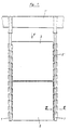
- the rod-like frames are each numbered 1 and the circuit boards held by them are numbered 2.
- pairs of clamping springs 3 belonging together are provided on the frames 1, which in this example are slightly angled and thus hold the circuit board inserted between them with resilient clamping force at point 4 (this is only schematic of FIG. 1) remove)).
- the corresponding position of the printed circuit board is shown in dash-dot lines in FIG. 3 by pressing the springs 3 apart. It can be seen that the shape of the springs 3 is such that the circuit boards either in the direction of arrow 5 or in the direction of arrow 6, i.e. can be pushed or pulled out parallel to the frames 1 between the pairs of springs.
- the springs are inserted with their ends 3 ⁇ into holes 7 of the respective frame 1 and held there.
- the electroplating current is supplied to the printed circuit boards 2 via the frames 1 and the springs 3.
- This insertion of the printed circuit boards between the springs is facilitated by funnel-shaped insertion openings 8 formed by the springs.
- 1 and 2 in particular show that the springs 3 extend freely from the frames 1, so that the frames 1 themselves do not impede the insertion of the printed circuit boards 2.
- the respective springs protrude into the space between the two frames 1, so that a uniform galvanization takes place.
- Fig. 1 also shows that several circuit boards can be arranged one above the other in a frame and that several circuit boards 2 can also be provided in the horizontal direction, since the frames can have a series of pairs of clamping springs arranged on top of each other (see that in Fig. 1 frame shown on the left).
- the frames and springs can be made of titanium.
- the use of stainless steel would also be possible. This also applies to the other exemplary embodiments.
- features described in one of the exemplary embodiments are used in a corresponding manner in other exemplary embodiments, or can be combined with features provided there.
- FIGS. 4 and 5 first shows a shape of the cross section of the frames 1, which also is advantageously provided in the other embodiments.
- This shape is elongated in the direction of the extent of the springs numbered 9 in this example, e.g. B. in the form of a rhombus, the long axis 10 of which runs in the direction of the springs.
- the circuit board 2 is again indicated by dash-dotted lines (in this position it keeps the springs 9 pressed apart). This achieves an advantageous, relatively low shielding of the galvanizing currents spreading in the manner of a field line with respect to the printed circuit board 2.
- a too strong shielding, as z. B. would be given by a square cross-sectional shape of the frame would have the consequence that too little electroplating material is applied to the edges of the circuit boards.
- the cross-sectional reinforcement of the frame 1 in the middle serves to increase its mechanical strength and better current conduction.
- the springs 9 are held with their two ends 9 ⁇ , 9 ⁇ in corresponding holes 11 in the frame 1, preferably under a prestress acting in the longitudinal direction of the spring, as a result of which special measures such as welding to hold the springs are unnecessary (see FIG. 5).
- Fig. 5 also shows a distance a between the opposing springs, whereby the circuit boards are easily inserted from each side in the direction of arrow 12.
- the springs 9 have inward or towards each other bulges 13, which are preferably (see also Fig. 5) offset from each other and hold the inserted circuit boards between them.
- the circuit boards can have at their side longitudinal edges 2 ⁇ one or more openings, preferably in the form of elongated holes, which engage in the clamped holding position of the plates via a support element of the respective frame and thus in addition to the clamp holder by the springs, a hold or securing of the circuit board 2 in their Represent the plating position. Exemplary embodiments of such an additional hold are shown in FIGS. 6-9 and in FIGS. 10, 11 and described below.
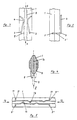
- FIGS. 6-9 shows printed circuit boards 2, on the longitudinal side edges 2 ⁇ of which a number of elongated holes 14 are provided. 6 shows that a frame 1 holds printed circuit boards 2 on each side (as has already been explained with reference to FIG. 1).
- two cooperating clamping springs 15, 16 are provided, of which the respective S-shaped spring 16 takes over the function of the support element. It is held with its end 16 ⁇ in a hole 18 of the frame 1.
- the spring 15 is inserted with its end 15 ⁇ in a corresponding hole 18.
- the height h of the S-shaped part of the spring 16 is dimensioned somewhat smaller than the length of the openings 14.
- a printed circuit board 2 indicated in FIG. 7 with the respective opening 14 in the direction of arrow 19 can be inserted over the S-shaped part (at the same time also via the S-shaped parts of the spring arrangements above or below). After that the printed circuit board 2 moves slightly downwards in the direction of arrow 20 until it assumes the dash-dotted position according to FIG. 7, in which its upper edge 14 ⁇ rests on the holding arm 16 ⁇ of the spring 16.
- FIG. 9 shows a section of the line IX-IX in FIG. 6, which also shows a variant in the cross-sectional design of the frame 1 (this cross section is not as elongated as in the exemplary embodiment of FIG. 4) .
- FIG. 8 is a view of FIG. 9 according to arrow VIII and FIG. 7 shows a view of FIG. 8 according to arrow VII.
- the springs 15, 16 are located inwards from frame 1 in the direction of the frame opposite (The springs are not shown in Fig. 6).
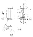
- spring pairs are provided on the frame 1 on the left and right, ie also directed towards the opposite frame, which consist of springs 21 fixedly attached to the frame and interact therewith but about the longitudinal axes 23 of shafts 24 exist with the shafts pivotable springs 22.
- 11 shows the pairs of springs 21, 22 in the clamping position.
- the circuit boards 2 assume the position indicated by dash-dotted lines, in which the clamping springs (see the illustration in FIG. 11) bear against the circuit board surfaces from the outside.
- holding or supporting pins 27 are also fastened to the frame 1, via which the plates 2 can be inserted with holes (not shown) in the operating position (clamping position) used for the galvanization.
- This plug connection secures the printed circuit boards 2 against falling during the assembly phases, in which the springs 21, 22 do not rest against the printed circuit boards with clamping force.
- the printed circuit boards do not have to be pushed from below or above in the longitudinal direction of the frames between clamping springs, but rather can be applied and removed frontally in a direction running transversely to their plate plane. This is necessary if there is no space for inserting the circuit boards from above or from below. Not only is it more convenient, but it is also usually faster than inserting it lengthways the racks.
- the frames are to be shaped in such a way that disadvantageous shielding of the goods to be electroplated from the electroplating current does not occur.
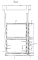
- a preferred embodiment of a frame 1 with two pivot shafts is described below with reference to FIGS. 16 to 18. This is to achieve the most favorable possible field distribution, that is to say the flow lines in the electroplating bath, and thus to prevent the frame and the swivel shafts from the printed circuit boards from shielding too many field lines during the electroplating process, which would result in inadequate electroplating of the edges of the printed circuit boards.
- the swivel shafts, numbered 24 ⁇ here are arranged on opposite sides of the rod-shaped frame 1, so that the central longitudinal axes 23 ⁇ of the swivel shafts 24 ⁇ are approximately aligned with the central longitudinal axis 1 ⁇ of the frame 1 and lie in one plane.
- the pivot shafts 24 ⁇ also run parallel to the frame 1. This results in a very elongated design that avoids the aforementioned disadvantages (see also the corresponding explanations for FIG. 4).
- FIG. 17 shows that, as a consequence of the above, in the clamp holder of the printed circuit boards 2 shown here in dash-dotted lines, they are aligned with the pivoting shafts 24 such and preferably also with the frame 1.
- the cohesion of the frame 1 and the two pivot shafts 24 ⁇ can be carried out in a structurally advantageous and simple embodiment with the aid of support and guide plates 33.
- the frame 1 passes through a hole in each of these plates 33 and is rigidly attached thereto, e.g. by means of a weld 34.
- the swivel shafts 24 are rotatably mounted, but are otherwise held in their position.
- a corresponding number of support and guide plates 33 are attached to the frames at intervals from one another.
- the support and guide plates 33 are also live (this is due to their rigid and at the same time conductive connection to the frames 1) and also abutments 36 for the printed circuit boards 2 in the clamping position shown.
- the opposite pole of the current transmission is formed by clamping springs 37 which are approximately U-shaped with a web 38 and angled legs 39.
- the legs 39 are fixed, at least in terms of rotational driving, firmly attached in the swivel shafts 24 ⁇ above and below the associated support and guide plate 3.
- the legs 39 are further angled so that their ends 38 'carrying the web 38' are directed towards the abutment 36 so that a perfect clamping of the printed circuit boards 2 is achieved (see in particular Fig. 17).
- the webs 38 run approximately in the longitudinal direction of the pivot shafts.
- Figs. 12 to 13 shows in side view (Fig. 12), end view (Fig. 13) and section (Fig. 14) that the springs 32 also as flat springs, i.e. can be made of flat steel strip.
- this idea of the invention can also be used in the other exemplary embodiments, i.e. taking over the spring designs described there and to. bring etc. be provided.
- the respective frame 1 consists of a copper core 27 with a coating 28 made of titanium. Furthermore, support arms 29 made of titanium are provided for the clamping springs 30, 31.
- the circuit boards are indicated with 2. Adverse voltage drops are avoided with this arrangement.
- printed circuit boards 2 can be held in a galvanic bath by the frames according to the invention both one above the other and next to one another.
- the frames 1 can be connected to each other in the usual way on the top by a frame support 1 ⁇ .
- All rack designs according to the invention can be cleaned (stripped) in the acid bath after removing the circuit boards. All racks can be easily insulated with a non-conductive acid-resistant coating so that unwanted galvanic deposits are avoided. Only the contact tips of the springs remain bare. The stripping (cleaning in the acid bath) is then limited to these contacts.
Landscapes
- Chemical & Material Sciences (AREA)
- Engineering & Computer Science (AREA)
- Chemical Kinetics & Catalysis (AREA)
- Electrochemistry (AREA)
- Materials Engineering (AREA)
- Metallurgy (AREA)
- Organic Chemistry (AREA)
- Manufacturing Of Printed Wiring (AREA)
- Electroplating Methods And Accessories (AREA)
- Devices For Use In Laboratory Experiments (AREA)
- Coupling Device And Connection With Printed Circuit (AREA)
Applications Claiming Priority (2)
| Application Number | Priority Date | Filing Date | Title |
|---|---|---|---|
| DE3606492 | 1986-02-28 | ||
| DE3606492 | 1986-02-28 |
Publications (3)
| Publication Number | Publication Date |
|---|---|
| EP0239736A1 EP0239736A1 (de) | 1987-10-07 |
| EP0239736B1 EP0239736B1 (de) | 1991-07-31 |
| EP0239736B2 true EP0239736B2 (de) | 1995-10-25 |
Family
ID=6295137
Family Applications (1)
| Application Number | Title | Priority Date | Filing Date |
|---|---|---|---|
| EP87101190A Expired - Lifetime EP0239736B2 (de) | 1986-02-28 | 1987-01-28 | Langgestreckte Gestelle und zugehörige Teile zum lösbaren Befestigen von zu galvanisierenden Leiterplatten, sowie zugehörige Leiterplatten |
Country Status (10)
| Country | Link |
|---|---|
| US (1) | US4752371A (ja) |
| EP (1) | EP0239736B2 (ja) |
| JP (1) | JPS62253800A (ja) |
| CN (1) | CN87100995A (ja) |
| AT (1) | AT398581B (ja) |
| BG (1) | BG60349B2 (ja) |
| CA (1) | CA1263480A (ja) |
| DE (2) | DE3771755D1 (ja) |
| ES (1) | ES2024439B3 (ja) |
| SU (1) | SU1554770A3 (ja) |
Families Citing this family (55)
| Publication number | Priority date | Publication date | Assignee | Title |
|---|---|---|---|---|
| DE8806806U1 (ja) * | 1988-05-25 | 1988-09-29 | H.-J. Metzka Gmbh, 8501 Schwand, De | |
| DE58905370D1 (de) * | 1988-07-07 | 1993-09-30 | Siemens Nixdorf Inf Syst | Galvanisiereinrichtung für plattenförmige Werkstücke, insbesondere Leiterplatten. |
| US4933049A (en) * | 1989-04-03 | 1990-06-12 | Unisys Corporation | Cradle for supporting printed circuit board between plating manifolds |
| GB8911566D0 (en) * | 1989-05-19 | 1989-07-05 | Sun Ind Coatings | Plating system |
| US5147050A (en) * | 1991-06-27 | 1992-09-15 | Surface Sciences, Inc. | Custom hanging rack with interchangeable support hooks and method therefor |
| DE9113516U1 (ja) * | 1991-10-30 | 1992-02-20 | Strecker, Guenther, 7100 Heilbronn, De | |
| AT399074B (de) * | 1991-12-23 | 1995-03-27 | Lenhard Ges M B H | Vorrichtung zum halten von leiterplatten |
| US5342495A (en) * | 1993-02-03 | 1994-08-30 | Vlsi Technology, Inc. | Structure for holding integrated circuit dies to be electroplated |
| US5524774A (en) * | 1994-07-28 | 1996-06-11 | Mighty Hook, Inc. | Hanging rack with cantilevered support hooks |
| FI953971A0 (fi) * | 1995-08-24 | 1995-08-24 | Galvatek Oy Ab | Apparatur foer faestande av en kropp pao sin plats foer elektrolytisk behandling |
| JP3328535B2 (ja) * | 1997-01-22 | 2002-09-24 | 秀行 小林 | 電気メッキ装置の製品搬送機構 |
| EP1052062A1 (en) * | 1999-05-03 | 2000-11-15 | Applied Materials, Inc. | Pré-conditioning fixed abrasive articles |
| CN1262690C (zh) * | 1999-10-12 | 2006-07-05 | 埃托特克德国有限公司 | 用于向待电解处理工件供电的载体和电解处理工件的方法 |
| US7303462B2 (en) * | 2000-02-17 | 2007-12-04 | Applied Materials, Inc. | Edge bead removal by an electro polishing process |
| US7678245B2 (en) * | 2000-02-17 | 2010-03-16 | Applied Materials, Inc. | Method and apparatus for electrochemical mechanical processing |
| US6979248B2 (en) * | 2002-05-07 | 2005-12-27 | Applied Materials, Inc. | Conductive polishing article for electrochemical mechanical polishing |
| US7077721B2 (en) | 2000-02-17 | 2006-07-18 | Applied Materials, Inc. | Pad assembly for electrochemical mechanical processing |
| US20050092621A1 (en) * | 2000-02-17 | 2005-05-05 | Yongqi Hu | Composite pad assembly for electrochemical mechanical processing (ECMP) |
| US7670468B2 (en) | 2000-02-17 | 2010-03-02 | Applied Materials, Inc. | Contact assembly and method for electrochemical mechanical processing |
| US7374644B2 (en) | 2000-02-17 | 2008-05-20 | Applied Materials, Inc. | Conductive polishing article for electrochemical mechanical polishing |
| US7125477B2 (en) | 2000-02-17 | 2006-10-24 | Applied Materials, Inc. | Contacts for electrochemical processing |
| US7029365B2 (en) | 2000-02-17 | 2006-04-18 | Applied Materials Inc. | Pad assembly for electrochemical mechanical processing |
| US7059948B2 (en) | 2000-12-22 | 2006-06-13 | Applied Materials | Articles for polishing semiconductor substrates |
| US6991528B2 (en) * | 2000-02-17 | 2006-01-31 | Applied Materials, Inc. | Conductive polishing article for electrochemical mechanical polishing |
| US7066800B2 (en) * | 2000-02-17 | 2006-06-27 | Applied Materials Inc. | Conductive polishing article for electrochemical mechanical polishing |
| US20040020789A1 (en) * | 2000-02-17 | 2004-02-05 | Applied Materials, Inc. | Conductive polishing article for electrochemical mechanical polishing |
| US7303662B2 (en) * | 2000-02-17 | 2007-12-04 | Applied Materials, Inc. | Contacts for electrochemical processing |
| US6962524B2 (en) * | 2000-02-17 | 2005-11-08 | Applied Materials, Inc. | Conductive polishing article for electrochemical mechanical polishing |
| SG85700A1 (en) * | 2000-03-15 | 2002-01-15 | Wus Printed Circuit Co Ltd | Multiple flat substrate electroplating apparatus |
| US7137879B2 (en) | 2001-04-24 | 2006-11-21 | Applied Materials, Inc. | Conductive polishing article for electrochemical mechanical polishing |
| US7344432B2 (en) | 2001-04-24 | 2008-03-18 | Applied Materials, Inc. | Conductive pad with ion exchange membrane for electrochemical mechanical polishing |
| US20050194681A1 (en) * | 2002-05-07 | 2005-09-08 | Yongqi Hu | Conductive pad with high abrasion |
| DE10241619B4 (de) * | 2002-09-04 | 2004-07-22 | Atotech Deutschland Gmbh | Vorrichtung und Verfahren zum elektrolytischen Behandeln von zumindest oberflächlich elektrisch leitfähigem Behandlungsgut |
| US7172184B2 (en) * | 2003-08-06 | 2007-02-06 | Sunpower Corporation | Substrate carrier for electroplating solar cells |
| DE10340888B3 (de) | 2003-09-04 | 2005-04-21 | Atotech Deutschland Gmbh | Stromversorgungseinrichtung in einer Vorrichtung zur elektrochemischen Behandlung |
| US7084064B2 (en) | 2004-09-14 | 2006-08-01 | Applied Materials, Inc. | Full sequence metal and barrier layer electrochemical mechanical processing |
| US7520968B2 (en) | 2004-10-05 | 2009-04-21 | Applied Materials, Inc. | Conductive pad design modification for better wafer-pad contact |
| US7427340B2 (en) * | 2005-04-08 | 2008-09-23 | Applied Materials, Inc. | Conductive pad |
| DE102005039100A1 (de) * | 2005-08-09 | 2007-02-15 | Gebr. Schmid Gmbh & Co. | Einrichtung zur Aufnahme bzw. Halterung mehrerer Substrate und Galvanisiereinrichtung |
| US20070096315A1 (en) * | 2005-11-01 | 2007-05-03 | Applied Materials, Inc. | Ball contact cover for copper loss reduction and spike reduction |
| DE102007026634B4 (de) * | 2007-06-06 | 2009-04-16 | Atotech Deutschland Gmbh | Vertikalanlage zur galvanotechnischen Behandlung eines Werkstückes und Verfahren zum Befördern des Werkstückes |
| DE102007026635B4 (de) * | 2007-06-06 | 2010-07-29 | Atotech Deutschland Gmbh | Vorrichtung zum nasschemischen Behandeln von Ware, Verwendung eines Strömungsorgans, Verfahren zum Einbauen eines Strömungsorgans in die Vorrichtung sowie Verfahren zur Herstellung einer nasschemisch behandelten Ware |
| CN101437365B (zh) * | 2007-11-15 | 2011-05-11 | 富葵精密组件(深圳)有限公司 | 固持装置及固持方法 |
| CN101713094B (zh) * | 2009-11-27 | 2011-10-26 | 深圳市五株电路板有限公司 | 印刷电路板电镀夹具 |
| DE202010001282U1 (de) * | 2010-01-20 | 2011-06-01 | Haga, Herbert, 72517 | Galvanikgestell |
| KR101317133B1 (ko) * | 2012-01-05 | 2013-10-08 | 주식회사 호진플라텍 | 태양전지용 전기 도금을 위한 기판 캐리어 장치 |
| US8956514B2 (en) * | 2012-11-09 | 2015-02-17 | Kohler Co. | Rack for coating components |
| CN103911640A (zh) * | 2013-01-05 | 2014-07-09 | 刘仁志 | 用于竖式槽进行印制线路板水平电镀的装置 |
| DE202015005883U1 (de) * | 2015-08-20 | 2016-11-23 | Bertold Oberle Ohg | Eintauchhalterung |
| CN105611740A (zh) * | 2016-03-30 | 2016-05-25 | 深圳市荣泰达节能机械设备有限公司 | 一种用于pcb双面阻焊和文字烘干的隧道炉 |
| CN108130584A (zh) * | 2018-01-19 | 2018-06-08 | 深圳崇达多层线路板有限公司 | 一种垂直连续式电镀铜设备中使用的电镀夹具 |
| US11598018B2 (en) * | 2018-03-30 | 2023-03-07 | Sunpower Corporation | Dual wafer plating fixture for a continuous plating line |
| RU191022U1 (ru) * | 2019-03-12 | 2019-07-19 | Общество с ограниченной ответственностью "Научный центр передовых технологий "СИРИУС" | Подвеска для гальванической обработки тонкостенных цилиндрических трубчатых деталей |
| CN110284176B (zh) * | 2019-07-09 | 2020-05-29 | 广德今腾电子科技有限公司 | 一种pcb板涂层的电镀装置及电镀工艺 |
| CN110366320B (zh) * | 2019-08-19 | 2022-03-25 | 江苏上达电子有限公司 | 改善柔性线路板翘曲的镀铜装置及其方法 |
Family Cites Families (22)
| Publication number | Priority date | Publication date | Assignee | Title |
|---|---|---|---|---|
| US3013959A (en) * | 1958-05-27 | 1961-12-19 | C & H Supply Company | Rack for supporting flat metal sheets in electrolytic operations |
| US3429786A (en) * | 1966-10-21 | 1969-02-25 | Gen Dynamics Corp | Controlled electroplating process |
| US3824176A (en) * | 1972-08-28 | 1974-07-16 | Buckbee Mears Co | Matrix holder |
| JPS5453636A (en) * | 1977-10-05 | 1979-04-27 | Kashita Seisakushiyo Kk | Hanger for plating |
| FR2419143A1 (fr) * | 1978-03-10 | 1979-10-05 | Neiman Sa | Dispositif de serrage |
| US4174262A (en) * | 1978-05-24 | 1979-11-13 | Mellaert Jozef K E H Van | Device for fastening at least one plate inside an electrolyte bath and for feeding current thereto |
| AT363749B (de) * | 1979-03-02 | 1981-08-25 | Kollmorgen Tech Corp | Gestell mit einer klemmvorrichtung zur verwendung in metallisierungsbaedern |
| DE3017853A1 (de) * | 1980-05-09 | 1981-11-12 | Günther 7100 Heilbronn Strecker | Galvanisiergestell mit gestellstab und gestellkopf |
| DD160317A3 (de) * | 1981-04-22 | 1983-06-01 | Herwig Fliegner | Haltevorrichtung fuer gegenstaende die mit elektrolytischen oder chemischen oberflaechenbehandlungen oder mit metallbedampfungstechnik bearbeitet werden sollen |
| DE3116897A1 (de) * | 1981-04-24 | 1982-11-11 | Schering Ag, 1000 Berlin Und 4619 Bergkamen | Gestell zum befestigen von leiterplatten |
| US4378281A (en) * | 1981-06-25 | 1983-03-29 | Napco, Inc. | High speed plating of flat planar workpieces |
| JPS5871395A (ja) * | 1981-10-22 | 1983-04-28 | Kiyoteru Takayasu | アルマイト加工用治具 |
| US4425212A (en) * | 1981-11-20 | 1984-01-10 | Francis William L | Electroplating device |
| US4534843A (en) * | 1983-01-28 | 1985-08-13 | Technic, Inc. | Apparatus for electroplating and chemically treating contact elements of encapsulated electronic components and their like |
| US4519887A (en) * | 1983-06-13 | 1985-05-28 | Think Laboratory Co., Ltd. | Apparatus for automatically attaching and detaching cassette-type rolls |
| DE3342712A1 (de) * | 1983-11-25 | 1985-06-05 | Strecker, Günther, 7100 Heilbronn | Gestellstab mit haltevorrichtung |
| CH659259A5 (fr) * | 1983-12-01 | 1987-01-15 | Em Microelectronic Marin Sa | Dispositif pour le depot electrolytique d'un materiau conducteur sur des plaques de circuits integres. |
| DD223737A1 (de) * | 1984-05-24 | 1985-06-19 | Robotron Zentrum Fuer Forschun | Anordnung zum einbringen von werkstuecken in badbehaelter einer galvanischen oberflaechenbehandlungsanlage |
| US4605483A (en) * | 1984-11-06 | 1986-08-12 | Michaelson Henry W | Electrode for electro-plating non-continuously conductive surfaces |
| AT381509B (de) * | 1985-02-06 | 1986-10-27 | Galvano Gestellbau Ing Rudolf | Vorrichtung zum halten von leiterplatten |
| JPS61217598A (ja) * | 1985-03-20 | 1986-09-27 | Mitsubishi Electric Corp | メツキ用引掛治具 |
| US4595480A (en) * | 1985-09-26 | 1986-06-17 | National Semiconductor Corporation | System for electroplating molded semiconductor devices |
-
1987
- 1987-01-28 ES ES87101190T patent/ES2024439B3/es not_active Expired - Lifetime
- 1987-01-28 DE DE8787101190T patent/DE3771755D1/de not_active Expired - Lifetime
- 1987-01-28 EP EP87101190A patent/EP0239736B2/de not_active Expired - Lifetime
- 1987-02-06 DE DE3703549A patent/DE3703549C2/de not_active Revoked
- 1987-02-26 BG BG78651A patent/BG60349B2/bg unknown
- 1987-02-27 JP JP62043252A patent/JPS62253800A/ja active Pending
- 1987-02-27 SU SU874202002A patent/SU1554770A3/ru active
- 1987-02-27 CN CN198787100995A patent/CN87100995A/zh active Pending
- 1987-02-27 CA CA000530809A patent/CA1263480A/en not_active Expired
- 1987-02-27 AT AT0044687A patent/AT398581B/de not_active IP Right Cessation
- 1987-03-02 US US07/023,132 patent/US4752371A/en not_active Expired - Fee Related
Also Published As
| Publication number | Publication date |
|---|---|
| DE3771755D1 (de) | 1991-09-05 |
| CA1263480A (en) | 1989-11-28 |
| US4752371A (en) | 1988-06-21 |
| DE3703549C2 (de) | 1994-05-19 |
| ES2024439B3 (es) | 1992-03-01 |
| BG60349B2 (bg) | 1994-06-30 |
| EP0239736B1 (de) | 1991-07-31 |
| EP0239736A1 (de) | 1987-10-07 |
| CN87100995A (zh) | 1988-03-16 |
| SU1554770A3 (ru) | 1990-03-30 |
| DE3703549A1 (de) | 1987-09-03 |
| AT398581B (de) | 1994-12-27 |
| ATA44687A (de) | 1989-07-15 |
| JPS62253800A (ja) | 1987-11-05 |
Similar Documents
| Publication | Publication Date | Title |
|---|---|---|
| EP0239736B2 (de) | Langgestreckte Gestelle und zugehörige Teile zum lösbaren Befestigen von zu galvanisierenden Leiterplatten, sowie zugehörige Leiterplatten | |
| EP0633330A1 (de) | Kontaktiereinrichtung für ein Leiterplattengestell einer Galvanikanlage | |
| EP0237736B1 (de) | Anordnung für das Bringen von zu galvanisierenden Teilen in ein bzw. aus einem Hängegestell | |
| EP0391085B1 (de) | Vorrichtung zum Befestigen und Wechseln von Werkzeugen | |
| EP0306719B1 (de) | Vorrichtung zum Abschaben fester Stoffe von einem Transportband | |
| EP0086954A2 (de) | Werkzeug zum Herausziehen eines Elektronikeinschubes aus einem Haltegestell | |
| EP0235552B1 (de) | Schalteranordnung | |
| AT391886B (de) | Haltezange | |
| AT506801B1 (de) | Nh-sicherungsschaltgerät | |
| EP0613837A1 (de) | Lager-und Transportgestell für Flächenbauteile | |
| EP0254056A1 (de) | Langgestreckte Gestelle mit Haltebügeln zum lösbaren Befestigen von Leiterplatten | |
| DE2553276C3 (de) | Haltevorrichtung für galvanisch zu behandelnde, insbesondere zu verchromende Kleinteile | |
| DE8220267U1 (de) | Verbindungsblock für Fernmeldeleitungen | |
| DE8610436U1 (de) | Einrichtung zum Fördern von langgestreckten Abschnitten und Abschnitthalter | |
| EP0524456A1 (de) | Vorpositionier- und Zustellvorrichtung für Webschäfte in Webmaschinen | |
| DE69838156T2 (de) | Elektronische Energieverteilungsvorrichtung | |
| DE2816952C2 (de) | Gelenkverbindung zur lösbaren Lagerung von Wendetafeln in Halteschienen | |
| DE102020112875B3 (de) | Lösbare Anbringung von Abstreifermodulen | |
| AT395919B (de) | Verfahren zur herstellung und zur verankerung von klemmhaltern fuer schmelzsicherungen | |
| DE3005613A1 (de) | Vorrichtung zur auswechselbaren halterung eines abstreifers eines werkzeugs an einem werkzeugtraeger einer metallbearbeitungsmaschine und werkzeug zur auswechslung des abstreifers | |
| DE3118156C2 (de) | Elektrodenanordnung in einer elektrischen Vielpunkt-Widerstandsschweißmaschine, insbesondere Gitterschweißmaschine | |
| DE4137618C2 (ja) | ||
| DE3805537A1 (de) | Greifvorrichtung, insbesondere roboterhand | |
| EP0560230A1 (de) | Befestigungssockel für Fiber-Optik-Anschlussmodule | |
| DE3112527C2 (de) | Magazin für einschiebbare elektrische Baugruppen |
Legal Events
| Date | Code | Title | Description |
|---|---|---|---|
| PUAI | Public reference made under article 153(3) epc to a published international application that has entered the european phase |
Free format text: ORIGINAL CODE: 0009012 |
|
| 17P | Request for examination filed |
Effective date: 19870128 |
|
| AK | Designated contracting states |
Kind code of ref document: A1 Designated state(s): BE CH DE ES FR GB IT LI LU NL SE |
|
| 17Q | First examination report despatched |
Effective date: 19901128 |
|
| GRAA | (expected) grant |
Free format text: ORIGINAL CODE: 0009210 |
|
| ITF | It: translation for a ep patent filed |
Owner name: ING. ZINI MARANESI & C. S.R.L. |
|
| AK | Designated contracting states |
Kind code of ref document: B1 Designated state(s): BE CH DE ES FR GB IT LI LU NL SE |
|
| REF | Corresponds to: |
Ref document number: 3771755 Country of ref document: DE Date of ref document: 19910905 |
|
| ET | Fr: translation filed | ||
| GBT | Gb: translation of ep patent filed (gb section 77(6)(a)/1977) | ||
| PLBI | Opposition filed |
Free format text: ORIGINAL CODE: 0009260 |
|
| 26 | Opposition filed |
Opponent name: LENHARD GMBH Effective date: 19920404 |
|
| NLR1 | Nl: opposition has been filed with the epo |
Opponent name: LENHARDT GMBH |
|
| PGFP | Annual fee paid to national office [announced via postgrant information from national office to epo] |
Ref country code: LU Payment date: 19931216 Year of fee payment: 8 |
|
| PGFP | Annual fee paid to national office [announced via postgrant information from national office to epo] |
Ref country code: BE Payment date: 19931227 Year of fee payment: 8 |
|
| PGFP | Annual fee paid to national office [announced via postgrant information from national office to epo] |
Ref country code: ES Payment date: 19940110 Year of fee payment: 8 |
|
| EPTA | Lu: last paid annual fee | ||
| REG | Reference to a national code |
Ref country code: GB Ref legal event code: 732E |
|
| REG | Reference to a national code |
Ref country code: FR Ref legal event code: TP |
|
| ITPR | It: changes in ownership of a european patent |
Owner name: CESSIONE;ATOTECH DEUTSCHLAND GMBH |
|
| NLS | Nl: assignments of ep-patents |
Owner name: ATOTECH DEUTSCHLAND GMBH TE BERLIJN, BONDSREPUBLIE |
|
| PG25 | Lapsed in a contracting state [announced via postgrant information from national office to epo] |
Ref country code: LU Free format text: LAPSE BECAUSE OF NON-PAYMENT OF DUE FEES Effective date: 19950128 |
|
| PG25 | Lapsed in a contracting state [announced via postgrant information from national office to epo] |
Ref country code: SE Free format text: LAPSE BECAUSE OF NON-PAYMENT OF DUE FEES Effective date: 19950129 |
|
| PG25 | Lapsed in a contracting state [announced via postgrant information from national office to epo] |
Ref country code: ES Free format text: LAPSE BECAUSE OF NON-PAYMENT OF DUE FEES Effective date: 19950130 |
|
| EAL | Se: european patent in force in sweden |
Ref document number: 87101190.4 |
|
| PG25 | Lapsed in a contracting state [announced via postgrant information from national office to epo] |
Ref country code: BE Effective date: 19950131 |
|
| REG | Reference to a national code |
Ref country code: ES Ref legal event code: PC2A Owner name: SCHERING AKTIENGESELLSCHAFT |
|
| BERE | Be: lapsed |
Owner name: SCHERING A.G. BERLIN UND BERGKAMEN Effective date: 19950131 |
|
| PUAH | Patent maintained in amended form |
Free format text: ORIGINAL CODE: 0009272 |
|
| STAA | Information on the status of an ep patent application or granted ep patent |
Free format text: STATUS: PATENT MAINTAINED AS AMENDED |
|
| 27A | Patent maintained in amended form |
Effective date: 19951025 |
|
| AK | Designated contracting states |
Kind code of ref document: B2 Designated state(s): BE CH DE ES FR GB IT LI LU NL SE |
|
| REG | Reference to a national code |
Ref country code: CH Ref legal event code: AEN Free format text: AUFRECHTERHALTUNG DES PATENTES IN GEAENDERTER FORM |
|
| NLR2 | Nl: decision of opposition | ||
| PGFP | Annual fee paid to national office [announced via postgrant information from national office to epo] |
Ref country code: SE Payment date: 19951218 Year of fee payment: 10 |
|
| ITF | It: translation for a ep patent filed |
Owner name: ING. ZINI MARANESI & C. S.R.L. |
|
| GBTA | Gb: translation of amended ep patent filed (gb section 77(6)(b)/1977) |
Effective date: 19960103 |
|
| ET3 | Fr: translation filed ** decision concerning opposition | ||
| NLR3 | Nl: receipt of modified translations in the netherlands language after an opposition procedure | ||
| REG | Reference to a national code |
Ref country code: ES Ref legal event code: FD2A Effective date: 20000503 |
|
| PGFP | Annual fee paid to national office [announced via postgrant information from national office to epo] |
Ref country code: FR Payment date: 20011210 Year of fee payment: 16 |
|
| PGFP | Annual fee paid to national office [announced via postgrant information from national office to epo] |
Ref country code: GB Payment date: 20011218 Year of fee payment: 16 |
|
| PGFP | Annual fee paid to national office [announced via postgrant information from national office to epo] |
Ref country code: NL Payment date: 20011219 Year of fee payment: 16 Ref country code: DE Payment date: 20011219 Year of fee payment: 16 Ref country code: CH Payment date: 20011219 Year of fee payment: 16 |
|
| REG | Reference to a national code |
Ref country code: GB Ref legal event code: IF02 |
|
| PG25 | Lapsed in a contracting state [announced via postgrant information from national office to epo] |
Ref country code: GB Free format text: LAPSE BECAUSE OF NON-PAYMENT OF DUE FEES Effective date: 20030128 |
|
| PG25 | Lapsed in a contracting state [announced via postgrant information from national office to epo] |
Ref country code: LI Free format text: LAPSE BECAUSE OF NON-PAYMENT OF DUE FEES Effective date: 20030131 Ref country code: CH Free format text: LAPSE BECAUSE OF NON-PAYMENT OF DUE FEES Effective date: 20030131 |
|
| PG25 | Lapsed in a contracting state [announced via postgrant information from national office to epo] |
Ref country code: NL Free format text: LAPSE BECAUSE OF NON-PAYMENT OF DUE FEES Effective date: 20030801 Ref country code: DE Free format text: LAPSE BECAUSE OF NON-PAYMENT OF DUE FEES Effective date: 20030801 |
|
| REG | Reference to a national code |
Ref country code: CH Ref legal event code: PL |
|
| GBPC | Gb: european patent ceased through non-payment of renewal fee | ||
| PG25 | Lapsed in a contracting state [announced via postgrant information from national office to epo] |
Ref country code: FR Free format text: LAPSE BECAUSE OF NON-PAYMENT OF DUE FEES Effective date: 20030930 |
|
| NLV4 | Nl: lapsed or anulled due to non-payment of the annual fee |
Effective date: 20030801 |
|
| REG | Reference to a national code |
Ref country code: FR Ref legal event code: ST |
|
| PG25 | Lapsed in a contracting state [announced via postgrant information from national office to epo] |
Ref country code: IT Free format text: LAPSE BECAUSE OF NON-PAYMENT OF DUE FEES;WARNING: LAPSES OF ITALIAN PATENTS WITH EFFECTIVE DATE BEFORE 2007 MAY HAVE OCCURRED AT ANY TIME BEFORE 2007. THE CORRECT EFFECTIVE DATE MAY BE DIFFERENT FROM THE ONE RECORDED. Effective date: 20050128 |