EP0226950A2 - Speicherzugriff-Steuerungsschaltung - Google Patents
Speicherzugriff-Steuerungsschaltung Download PDFInfo
- Publication number
- EP0226950A2 EP0226950A2 EP86117189A EP86117189A EP0226950A2 EP 0226950 A2 EP0226950 A2 EP 0226950A2 EP 86117189 A EP86117189 A EP 86117189A EP 86117189 A EP86117189 A EP 86117189A EP 0226950 A2 EP0226950 A2 EP 0226950A2
- Authority
- EP
- European Patent Office
- Prior art keywords
- address
- signal
- memory
- signals
- access
- Prior art date
- Legal status (The legal status is an assumption and is not a legal conclusion. Google has not performed a legal analysis and makes no representation as to the accuracy of the status listed.)
- Granted
Links
Images


Classifications
-
- G—PHYSICS
- G06—COMPUTING OR CALCULATING; COUNTING
- G06F—ELECTRIC DIGITAL DATA PROCESSING
- G06F12/00—Accessing, addressing or allocating within memory systems or architectures
- G06F12/02—Addressing or allocation; Relocation
- G06F12/0215—Addressing or allocation; Relocation with look ahead addressing means
Definitions
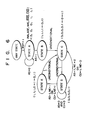
- Upper and lower memory address signals UMA and LMA are supplied from address counter 12 to multiplexer 13.
- Multiplexer 13 time-divisionally sends address signals UMA and LMA onto address bus 14 in response to address switching signal ASE (to be described later).
Landscapes
- Engineering & Computer Science (AREA)
- Theoretical Computer Science (AREA)
- Physics & Mathematics (AREA)
- General Engineering & Computer Science (AREA)
- General Physics & Mathematics (AREA)
- Dram (AREA)
- Memory System (AREA)
Applications Claiming Priority (2)
| Application Number | Priority Date | Filing Date | Title |
|---|---|---|---|
| JP60290209A JPS62149099A (ja) | 1985-12-23 | 1985-12-23 | メモリアクセス制御回路 |
| JP290209/85 | 1985-12-23 |
Publications (3)
| Publication Number | Publication Date |
|---|---|
| EP0226950A2 true EP0226950A2 (de) | 1987-07-01 |
| EP0226950A3 EP0226950A3 (en) | 1990-01-17 |
| EP0226950B1 EP0226950B1 (de) | 1993-02-17 |
Family
ID=17753159
Family Applications (1)
| Application Number | Title | Priority Date | Filing Date |
|---|---|---|---|
| EP86117189A Expired - Lifetime EP0226950B1 (de) | 1985-12-23 | 1986-12-10 | Speicherzugriff-Steuerungsschaltung |
Country Status (4)
| Country | Link |
|---|---|
| US (1) | US4839856A (de) |
| EP (1) | EP0226950B1 (de) |
| JP (1) | JPS62149099A (de) |
| DE (1) | DE3687787T2 (de) |
Cited By (6)
| Publication number | Priority date | Publication date | Assignee | Title |
|---|---|---|---|---|
| WO1989001204A1 (en) * | 1987-07-23 | 1989-02-09 | Ncr Corporation | Memory access for a computer system |
| WO1993024885A1 (en) * | 1992-06-04 | 1993-12-09 | Cabletron Systems, Inc. | Adaptive memory controller |
| EP0549633A4 (de) * | 1990-09-04 | 1994-02-23 | Gilbert P. Hyatt | |
| WO1996008768A1 (en) * | 1994-09-16 | 1996-03-21 | Philips Electronics N.V. | Microcontroller conditionally skips updating latch for msb and directly drives lsb of memory address |
| US5602999A (en) * | 1970-12-28 | 1997-02-11 | Hyatt; Gilbert P. | Memory system having a plurality of memories, a plurality of detector circuits, and a delay circuit |
| EP0444885B1 (de) * | 1990-03-02 | 1999-05-06 | Seagate Technology International | Verfahren zum Steuern eines Pufferspeichers für einen Magnetplattenspeicher |
Families Citing this family (25)
| Publication number | Priority date | Publication date | Assignee | Title |
|---|---|---|---|---|
| US5058005A (en) * | 1988-09-09 | 1991-10-15 | Compaq Computer Corporation | Computer system with high speed data transfer capabilities |
| US5159676A (en) * | 1988-12-05 | 1992-10-27 | Micron Technology, Inc. | Semi-smart DRAM controller IC to provide a pseudo-cache mode of operation using standard page mode draws |
| CA2011518C (en) * | 1989-04-25 | 1993-04-20 | Ronald N. Fortino | Distributed cache dram chip and control method |
| US6564308B2 (en) | 1989-05-05 | 2003-05-13 | Samsung Electronics Co. Ltd. | Multiple mode memory module |
| US5261073A (en) * | 1989-05-05 | 1993-11-09 | Wang Laboratories, Inc. | Method and apparatus for providing memory system status signals |
| JP2679296B2 (ja) * | 1989-09-13 | 1997-11-19 | 日産自動車株式会社 | キックダウンスイッチの取付構造 |
| JPH03113794A (ja) * | 1989-09-22 | 1991-05-15 | Toshiba Corp | 半導体記憶装置 |
| US5276856A (en) * | 1989-09-28 | 1994-01-04 | Pixel Semiconductor, Inc. | Memory controller flexible timing control system and method |
| JP2925600B2 (ja) * | 1989-11-07 | 1999-07-28 | 富士通株式会社 | 半導体記憶装置 |
| JPH047761A (ja) * | 1990-04-26 | 1992-01-13 | Fuji Xerox Co Ltd | メモリアクセス方法 |
| JPH0682339B2 (ja) * | 1990-08-31 | 1994-10-19 | インターナショナル・ビジネス・マシーンズ・コーポレイション | メモリ・アクセス・システムおよび方法 |
| US5265236A (en) * | 1990-11-29 | 1993-11-23 | Sun Microsystems, Inc. | Method and apparatus for increasing the speed of memory access in a virtual memory system having fast page mode |
| US5253214A (en) * | 1991-09-27 | 1993-10-12 | Eastman Kodak Company | High-performance memory controller with application-programmable optimization |
| US5485589A (en) * | 1991-12-31 | 1996-01-16 | Dell Usa, L.P. | Predictive addressing architecture |
| JP2729126B2 (ja) * | 1992-03-24 | 1998-03-18 | 富士通株式会社 | デバッグ・システムのアドレス・トレース回路 |
| US5715421A (en) * | 1992-10-16 | 1998-02-03 | Seiko Epson Corporation | Apparatus and method of addressing paged mode memory including adjacent page precharging |
| JPH07281948A (ja) * | 1994-04-06 | 1995-10-27 | Mitsubishi Electric Corp | メモリ制御装置 |
| TW267222B (en) * | 1994-10-05 | 1996-01-01 | Ibm | Improved method and system of addressing |
| US5678017A (en) | 1995-03-24 | 1997-10-14 | Micron Technology, Inc. | Automatic reloading of serial read operation pipeline on last bit transfers to serial access memory in split read transfer operations |
| US5895480A (en) * | 1995-10-10 | 1999-04-20 | Holtek Microelectronics, Inc. | Method of and means for accessing an address by respectively substracting base addresses of memory integrated circuits from an access address |
| US6209071B1 (en) | 1996-05-07 | 2001-03-27 | Rambus Inc. | Asynchronous request/synchronous data dynamic random access memory |
| JP3454094B2 (ja) | 1997-07-22 | 2003-10-06 | 日本電気株式会社 | 共有メモリ制御装置および共有メモリ制御方法 |
| AU9798798A (en) | 1997-10-10 | 1999-05-03 | Rambus Incorporated | Power control system for synchronous memory device |
| US6477630B2 (en) | 1999-02-24 | 2002-11-05 | International Business Machines Corporation | Hierarchical row activation method for banking control in multi-bank DRAM |
| TWI397855B (zh) * | 2008-05-07 | 2013-06-01 | Sunplus Mmedia Inc | 減少接腳數之方法以及使用其之微處理器 |
Family Cites Families (10)
| Publication number | Priority date | Publication date | Assignee | Title |
|---|---|---|---|---|
| US4156905A (en) * | 1974-02-28 | 1979-05-29 | Ncr Corporation | Method and apparatus for improving access speed in a random access memory |
| JPS5916354B2 (ja) * | 1978-10-17 | 1984-04-14 | 日本電信電話株式会社 | 記憶装置 |
| JPS5943786B2 (ja) * | 1979-03-30 | 1984-10-24 | パナフアコム株式会社 | 記憶装置のアクセス方式 |
| US4495565A (en) * | 1981-11-09 | 1985-01-22 | At&T Bell Laboratories | Computer memory address matcher and process |
| GB2112256B (en) * | 1981-11-18 | 1985-11-06 | Texas Instruments Ltd | Memory apparatus |
| US4546451A (en) * | 1982-02-12 | 1985-10-08 | Metheus Corporation | Raster graphics display refresh memory architecture offering rapid access speed |
| JPS593790A (ja) * | 1982-06-30 | 1984-01-10 | Yokogawa Hokushin Electric Corp | ダイナミツクメモリ素子を用いた記憶装置 |
| JPS60258792A (ja) * | 1984-06-04 | 1985-12-20 | Toshiba Corp | ダイナミツクram |
| JPS6199996A (ja) * | 1984-10-19 | 1986-05-19 | Ricoh Co Ltd | ダイナミツクram制御方式 |
| US4701843A (en) * | 1985-04-01 | 1987-10-20 | Ncr Corporation | Refresh system for a page addressable memory |
-
1985
- 1985-12-23 JP JP60290209A patent/JPS62149099A/ja active Pending
-
1986
- 1986-12-10 DE DE8686117189T patent/DE3687787T2/de not_active Expired - Fee Related
- 1986-12-10 EP EP86117189A patent/EP0226950B1/de not_active Expired - Lifetime
- 1986-12-11 US US06/940,725 patent/US4839856A/en not_active Expired - Lifetime
Cited By (7)
| Publication number | Priority date | Publication date | Assignee | Title |
|---|---|---|---|---|
| US5526506A (en) * | 1970-12-28 | 1996-06-11 | Hyatt; Gilbert P. | Computer system having an improved memory architecture |
| US5602999A (en) * | 1970-12-28 | 1997-02-11 | Hyatt; Gilbert P. | Memory system having a plurality of memories, a plurality of detector circuits, and a delay circuit |
| WO1989001204A1 (en) * | 1987-07-23 | 1989-02-09 | Ncr Corporation | Memory access for a computer system |
| EP0444885B1 (de) * | 1990-03-02 | 1999-05-06 | Seagate Technology International | Verfahren zum Steuern eines Pufferspeichers für einen Magnetplattenspeicher |
| EP0549633A4 (de) * | 1990-09-04 | 1994-02-23 | Gilbert P. Hyatt | |
| WO1993024885A1 (en) * | 1992-06-04 | 1993-12-09 | Cabletron Systems, Inc. | Adaptive memory controller |
| WO1996008768A1 (en) * | 1994-09-16 | 1996-03-21 | Philips Electronics N.V. | Microcontroller conditionally skips updating latch for msb and directly drives lsb of memory address |
Also Published As
| Publication number | Publication date |
|---|---|
| DE3687787T2 (de) | 1993-06-24 |
| JPS62149099A (ja) | 1987-07-03 |
| EP0226950A3 (en) | 1990-01-17 |
| US4839856A (en) | 1989-06-13 |
| EP0226950B1 (de) | 1993-02-17 |
| DE3687787D1 (de) | 1993-03-25 |
Similar Documents
| Publication | Publication Date | Title |
|---|---|---|
| EP0226950B1 (de) | Speicherzugriff-Steuerungsschaltung | |
| US4660181A (en) | Memory system | |
| EP0025801A1 (de) | Zugriffssystem für speichermodule | |
| JPH04293144A (ja) | コンピュータシステム | |
| EP0364110B1 (de) | Halbleiterspeichereinrichtung, die einen Speicher mit Seriengriff aufweist | |
| US3704452A (en) | Shift register storage unit | |
| EP0057096A2 (de) | Informationsverarbeitungsanlage | |
| US6292853B1 (en) | DMA controller adapted for transferring data in two-dimensional mapped address space | |
| KR920003699B1 (ko) | 레지스터회로 | |
| JP2827361B2 (ja) | 半導体メモリ装置 | |
| JPS63191397A (ja) | 情報処理装置 | |
| JP3947856B2 (ja) | データ設定制御装置 | |
| KR100205589B1 (ko) | 타임스위치의 메모리 억세스회로 | |
| SU1487101A1 (ru) | Устройство для управления регенерацией динамической памяти | |
| JPS63163938A (ja) | ダイナミツクramコントロ−ラ | |
| JPH05210572A (ja) | メモリ制御装置 | |
| KR880000995B1 (ko) | 기억장치 | |
| GB2084771A (en) | Improvements in or relating to circuit arrangements for detecting malfunctioning in direct data controllers of microprocessor systems | |
| JPH04153984A (ja) | ダイナミックメモリの制御方法 | |
| JP2621361B2 (ja) | 図形処理装置 | |
| JPH07191099A (ja) | Ic検査装置 | |
| JPS63191398A (ja) | 情報処理装置 | |
| JPH0689237A (ja) | メモリ制御システム | |
| JPH01112449A (ja) | 速度変換メモリ装置 | |
| JP2004118595A (ja) | アクセス制御装置及びアクセス制御方法 |
Legal Events
| Date | Code | Title | Description |
|---|---|---|---|
| PUAI | Public reference made under article 153(3) epc to a published international application that has entered the european phase |
Free format text: ORIGINAL CODE: 0009012 |
|
| 17P | Request for examination filed |
Effective date: 19870107 |
|
| AK | Designated contracting states |
Kind code of ref document: A2 Designated state(s): DE FR GB |
|
| PUAL | Search report despatched |
Free format text: ORIGINAL CODE: 0009013 |
|
| AK | Designated contracting states |
Kind code of ref document: A3 Designated state(s): DE FR GB |
|
| 17Q | First examination report despatched |
Effective date: 19910426 |
|
| GRAA | (expected) grant |
Free format text: ORIGINAL CODE: 0009210 |
|
| AK | Designated contracting states |
Kind code of ref document: B1 Designated state(s): DE FR GB |
|
| REF | Corresponds to: |
Ref document number: 3687787 Country of ref document: DE Date of ref document: 19930325 |
|
| ET | Fr: translation filed | ||
| PLBE | No opposition filed within time limit |
Free format text: ORIGINAL CODE: 0009261 |
|
| STAA | Information on the status of an ep patent application or granted ep patent |
Free format text: STATUS: NO OPPOSITION FILED WITHIN TIME LIMIT |
|
| 26N | No opposition filed | ||
| PGFP | Annual fee paid to national office [announced via postgrant information from national office to epo] |
Ref country code: GB Payment date: 19971201 Year of fee payment: 12 |
|
| PGFP | Annual fee paid to national office [announced via postgrant information from national office to epo] |
Ref country code: FR Payment date: 19971209 Year of fee payment: 12 |
|
| PGFP | Annual fee paid to national office [announced via postgrant information from national office to epo] |
Ref country code: DE Payment date: 19971222 Year of fee payment: 12 |
|
| PG25 | Lapsed in a contracting state [announced via postgrant information from national office to epo] |
Ref country code: GB Free format text: LAPSE BECAUSE OF NON-PAYMENT OF DUE FEES Effective date: 19981210 |
|
| GBPC | Gb: european patent ceased through non-payment of renewal fee |
Effective date: 19981210 |
|
| PG25 | Lapsed in a contracting state [announced via postgrant information from national office to epo] |
Ref country code: FR Free format text: LAPSE BECAUSE OF NON-PAYMENT OF DUE FEES Effective date: 19990831 |
|
| REG | Reference to a national code |
Ref country code: FR Ref legal event code: ST |
|
| PG25 | Lapsed in a contracting state [announced via postgrant information from national office to epo] |
Ref country code: DE Free format text: LAPSE BECAUSE OF NON-PAYMENT OF DUE FEES Effective date: 19991001 |