EP0099100A1 - Gateschaltung mit Feldeffekt- und Bipolartransistoren - Google Patents
Gateschaltung mit Feldeffekt- und Bipolartransistoren Download PDFInfo
- Publication number
- EP0099100A1 EP0099100A1 EP83106796A EP83106796A EP0099100A1 EP 0099100 A1 EP0099100 A1 EP 0099100A1 EP 83106796 A EP83106796 A EP 83106796A EP 83106796 A EP83106796 A EP 83106796A EP 0099100 A1 EP0099100 A1 EP 0099100A1
- Authority
- EP
- European Patent Office
- Prior art keywords
- effect
- base
- bipolar transistor
- drain
- channel field
- Prior art date
- Legal status (The legal status is an assumption and is not a legal conclusion. Google has not performed a legal analysis and makes no representation as to the accuracy of the status listed.)
- Granted
Links
- 230000005669 field effect Effects 0.000 title claims description 15
- 238000007599 discharging Methods 0.000 claims abstract description 18
- 230000004888 barrier function Effects 0.000 claims description 6
- 230000000295 complement effect Effects 0.000 abstract description 3
- 238000010586 diagram Methods 0.000 description 16
- 239000004065 semiconductor Substances 0.000 description 10
- 239000002184 metal Substances 0.000 description 6
- 229910052710 silicon Inorganic materials 0.000 description 6
- 239000010703 silicon Substances 0.000 description 6
- 238000010276 construction Methods 0.000 description 3
- 230000000694 effects Effects 0.000 description 3
- 230000003321 amplification Effects 0.000 description 2
- 230000003247 decreasing effect Effects 0.000 description 2
- 230000006870 function Effects 0.000 description 2
- 230000036039 immunity Effects 0.000 description 2
- 230000010354 integration Effects 0.000 description 2
- 238000003199 nucleic acid amplification method Methods 0.000 description 2
- 239000000758 substrate Substances 0.000 description 2
- 230000003111 delayed effect Effects 0.000 description 1
- 239000000284 extract Substances 0.000 description 1
- 238000000605 extraction Methods 0.000 description 1
- 229910044991 metal oxide Inorganic materials 0.000 description 1
- 150000004706 metal oxides Chemical class 0.000 description 1
- 238000012986 modification Methods 0.000 description 1
- 230000004048 modification Effects 0.000 description 1
Images


Classifications
-
- H—ELECTRICITY
- H03—ELECTRONIC CIRCUITRY
- H03K—PULSE TECHNIQUE
- H03K19/00—Logic circuits, i.e. having at least two inputs acting on one output; Inverting circuits
-
- H—ELECTRICITY
- H01—ELECTRIC ELEMENTS
- H01L—SEMICONDUCTOR DEVICES NOT COVERED BY CLASS H10
- H01L27/00—Devices consisting of a plurality of semiconductor or other solid-state components formed in or on a common substrate
- H01L27/02—Devices consisting of a plurality of semiconductor or other solid-state components formed in or on a common substrate including semiconductor components specially adapted for rectifying, oscillating, amplifying or switching and having potential barriers; including integrated passive circuit elements having potential barriers
- H01L27/04—Devices consisting of a plurality of semiconductor or other solid-state components formed in or on a common substrate including semiconductor components specially adapted for rectifying, oscillating, amplifying or switching and having potential barriers; including integrated passive circuit elements having potential barriers the substrate being a semiconductor body
- H01L27/06—Devices consisting of a plurality of semiconductor or other solid-state components formed in or on a common substrate including semiconductor components specially adapted for rectifying, oscillating, amplifying or switching and having potential barriers; including integrated passive circuit elements having potential barriers the substrate being a semiconductor body including a plurality of individual components in a non-repetitive configuration
- H01L27/0611—Devices consisting of a plurality of semiconductor or other solid-state components formed in or on a common substrate including semiconductor components specially adapted for rectifying, oscillating, amplifying or switching and having potential barriers; including integrated passive circuit elements having potential barriers the substrate being a semiconductor body including a plurality of individual components in a non-repetitive configuration integrated circuits having a two-dimensional layout of components without a common active region
- H01L27/0617—Devices consisting of a plurality of semiconductor or other solid-state components formed in or on a common substrate including semiconductor components specially adapted for rectifying, oscillating, amplifying or switching and having potential barriers; including integrated passive circuit elements having potential barriers the substrate being a semiconductor body including a plurality of individual components in a non-repetitive configuration integrated circuits having a two-dimensional layout of components without a common active region comprising components of the field-effect type
- H01L27/0623—Devices consisting of a plurality of semiconductor or other solid-state components formed in or on a common substrate including semiconductor components specially adapted for rectifying, oscillating, amplifying or switching and having potential barriers; including integrated passive circuit elements having potential barriers the substrate being a semiconductor body including a plurality of individual components in a non-repetitive configuration integrated circuits having a two-dimensional layout of components without a common active region comprising components of the field-effect type in combination with bipolar transistors
-
- H—ELECTRICITY
- H03—ELECTRONIC CIRCUITRY
- H03K—PULSE TECHNIQUE
- H03K19/00—Logic circuits, i.e. having at least two inputs acting on one output; Inverting circuits
- H03K19/01—Modifications for accelerating switching
-
- H—ELECTRICITY
- H03—ELECTRONIC CIRCUITRY
- H03K—PULSE TECHNIQUE
- H03K19/00—Logic circuits, i.e. having at least two inputs acting on one output; Inverting circuits
- H03K19/01—Modifications for accelerating switching
- H03K19/017—Modifications for accelerating switching in field-effect transistor circuits
- H03K19/01707—Modifications for accelerating switching in field-effect transistor circuits in asynchronous circuits
- H03K19/01721—Modifications for accelerating switching in field-effect transistor circuits in asynchronous circuits by means of a pull-up or down element
-
- H—ELECTRICITY
- H03—ELECTRONIC CIRCUITRY
- H03K—PULSE TECHNIQUE
- H03K19/00—Logic circuits, i.e. having at least two inputs acting on one output; Inverting circuits
- H03K19/02—Logic circuits, i.e. having at least two inputs acting on one output; Inverting circuits using specified components
- H03K19/08—Logic circuits, i.e. having at least two inputs acting on one output; Inverting circuits using specified components using semiconductor devices
- H03K19/094—Logic circuits, i.e. having at least two inputs acting on one output; Inverting circuits using specified components using semiconductor devices using field-effect transistors
- H03K19/0944—Logic circuits, i.e. having at least two inputs acting on one output; Inverting circuits using specified components using semiconductor devices using field-effect transistors using MOSFET or insulated gate field-effect transistors, i.e. IGFET
- H03K19/09448—Logic circuits, i.e. having at least two inputs acting on one output; Inverting circuits using specified components using semiconductor devices using field-effect transistors using MOSFET or insulated gate field-effect transistors, i.e. IGFET in combination with bipolar transistors [BIMOS]
Definitions
- This invention relates to gate circuits, and more particularly to a gate circuit formed of a combination of field-effect. transistors and bipolar transistors.
- This inventor circuit is formed of a P-channel metal (silicon)-oxide-semiconductor field-effect-transistor (hereinafter, referred to simply as PMOS) 50, an N-channel metal (silicon) oxide-semiconductor field-effect-transistor (hereinafter, referred to simply as NMOS) 51, an NPN transistor (hereinafter, referred to simply as NPN) 53, and a PNP transistor (hereinafter, referred to simply as PNP) 54.
- PMOS P-channel metal (silicon)-oxide-semiconductor field-effect-transistor
- NMOS N-channel metal oxide-semiconductor field-effect-transistor
- NPN NPN transistor
- PNP PNP transistor
- the bipolar transistors NPN 53 and PNP 54 used are complementary and difficult to be matched in their switching characteristics, the trailing edge of the output signal 56 is delayed. This is because the NPN involved in the complementary transistors is inferior in performances such as current amplification factor to NPN.
- NOR gate circuit shown in Fig. 2a (IEEE. Trans. Electron Devices, vol. ED-16, No. 11, pp. 945-951, Nov. 1969).
- This two-input NOR circuit is a combination of a C-MOS transistor NOR gate circuit having PMOSs 200 and 201 and NMOSs 202 and 203 as shown in Fig. 2b, and NPNs 301 and 302.
- the time required for the switching from the on-state to the off-state is long because of no means for forcibly extracting or drawing out minority charges accumulated on the bases of the NPNs 301 and 302.
- the first and second NPNs 301 and 302 stay long in the on-state, so that the switching time as well as the power consumption increases.
- a high-speed, low-power consumption gate circuit capable of preventing first and second bipolar transistors from simultaneously turning on by providing the gate circuit of combined field-effect transistors and bipolar transistors with discharge means for discharging accumulated charges from the transistors when the field-effect transistors and bipolar transistors are turned off.
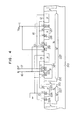
- Fig. 3 shows an inverter circuit of the first embodiment of this invention.
- first NPN NPN bipolar transistor
- second NPN NPN bipolar transistor
- Shown at 10 is a P-channel metal (silicon)-oxide-semiconductor field-effect-transistor (hereinafter, referred to simply as PMOS) having its gate G connected to an input terminal 16 and its source S and drain D respectively connected to the collector C and base B of the first NPN.
- Shown at 11 is an N-channel metal (silicon)-oxide-semiconductor field-effect-transistor (hereinafter, referred simply as NMOS) having its gate G connected to the input terminal 16, and its drain D and source S respectively connected to the collector C and base B of the second NPN.
- Shown at 12 is a resistor connecting the drain D of the PMOS 10 with the drain D of the NMOS 11 and at 13 is a resistor connecting the base B with emitter E of the second NPN 15.
- Fig. 4 schematically shows the cross-section of a semiconductor integrated circuit structure of the inverter circuit illustrated in Fig. 3.
- the PMOS 10, first NPN 14, resistors 12 and 13 and NMOS 11 are formed in an island 212 of a semiconductor substrate 210, and the second NPN 15 in an island 213 thereof. Shown at 227 is a buried layer.
- a P region 219 and a gate electrode G constitute the PMOS 10 and an N + region 223 and a gate electrode G within a P well 214 constitute the NMOS 11.
- the first NPN 14 comprises a P region 217, as its base B, an N + region 218 within the P region 217 as its emitter E and an N + region 215 as its collector C.
- the second NPN 15 comprises a P region 225 within the island 213 as its base B, an N + region 226 within the P region 225 as its emitter E, and an N' region 224 as its collector C.
- Table 1 lists the logic operations of the inverter circuit of this embodiment.
- the emitter current of the first NPN 14 charges the load (not shown) and the output turminal 17 rapidly becomes at "1" level.
- the PMOS 10 When the input terminal 16 is at "1" level, the PMOS 10 is made off but the NMOS 11 on. At this time, since the PMOS 10 is off, the current to the NPN 14 stops and the charges stored on the base B of the first NPN 14 and in the drain D of the PMOS 10 are drawn out through the resistors 12 and 13 to the ground, so that the first NPN 14 is rapidly turned off.
- the NMOS 11 since the NMOS 11 is on to form a short circuit between its drain D and source S, the second NPN 15 is supplied at its base B with the current from the output terminal 17 and with the charges stored in the base B of the first NPN 14 and in the drain D of the PMOS 10 as mentioned above, and thereby the NPN 15 is rapidly turned on. Consequently, the output terminal 17 rapidly becomes at "0" level.
- the resistor 12 extracts the charges accumulated in the drain D of the PMOS 10 and in the base B of the first NPN 14 to rapidly turn off the first NPN 14 and supplies the extracted charges via the NMOS 11 in the on-state to the base B of the second NPN 15 to rapidly turn on the second NPN 15.
- the resistor 12 is provided between the drain D of the PMOS 10 and the drain D of the NMOS 11, a conductive path for causing short-circuiting is not formed between the power terminal 1 and GND and thus low-power consumption in the C-MOS circuit can be achieved.
- the resistor 12 were connected between the drain D of the PMOS 10 and GND, a conductive path would be formed between the power terminal 1 and GND when the input terminal 16 is at "0" level, and thus current would always flow therethrough to increase power consumption.
- the resistor 12 is also connected to the output terminal 17, the potential at the output terminal 17, when the input terminal 16 is at "0" level, can be raised to the potential at the power terminal 1 through the PMOS 10 and resistor 12, assuring enough noise immunity.
- the resistor 13 when the NMOS 11 and second NPN 15 are switched from on-state to off-state, discharges the charges accumulated in the base B of the second NPN 15 so as to rapidly turn off the second NPN 15. Also, in this embodiment, when the input terminal 16 is at "1" level, the output terminal 17 can be decreased to "0" level through the resistor 13 and NMOS 11, assuring enough noise immunity.
- the bipolar transistors used are of the same NPN-type, and are thus advantageous in making the switching characteristics easily uniform to each other.
- Fig. 5 shows a two-input NAND circuit of a second embodiment of this invention.
- a first NPN 26 having its collector C connected to the power supply terminal 1, and its emitter E connected to an output terminal 29, a second NPN 27 having its collector C connected to an output terminal 29 and its emitter E connected to a ground potential GND, and two input terminals 28.
- PMOSs having their gates G connected respectively to one and the other of the input terminals 28, and their source S - drain D paths connected in parallel between the collector C and base B of the first NPN 26, and at 22 and 23 are NMOSs having their gates G connected respectively to one and the other of the input terminals 28 and their drain D - source S paths connect in series between the collector C and base B of the second NPN 27.
- Table 2 shows the logic operations of this embodiment.
- the emitter current of the first NPN 26 charges the load to rapidly raise the potential of the output end 29 to "1" level.
- both of the input terminals 28 are at "0" level, both the PMOSs 20 and 21 are turned on and both the NMOSs 22 and 23 are turned off. Thus, the operation is the same as above, the output terminal 29 becoming at "1" level.
- both the input terminals 28 are at "1" level, both of the PMOSs 20 and 21 are turned off, and both NMOSs 22 and 23 are turned on.
- both the PMOSs 20 and 21 are turned off, current to the first NPN 26 stops flowing and the charges accumulated in the base B of the first NPN 26 are extracted, so that the first NPN 26 is rapidly turned off.
- the NMOSs 22 and 23 are turned on to form short circuit between the drains D and sources S, the second NPN 27 is supplied at its base B with the current from the output terminal 29 and with discharge current from the base B of the first NPN 26 as described previously so as to rapidly turn on.
- the output terminal 29 rapidly becomes at "0" level.
- a 2-input NAND circuit is described as an example, a 3-input, 4-input or generally k-input NAND circuit (k ⁇ 22) can be used as an example of this invention.
- Fig. 6 shows a two-input NOR circuit of a third embodiment of this invention.
- reference numeral 36 represents a first NPN having its collector C connected to power terminal 1 and its emitter E connected to an output terminal 39, 37 a second NPN having its collector C connected to the output terminal 39 and its emitter E connected to ground potential GND, 38 two input terminals, 30 and 31 PMOSs having their gates G connected to one and the other of the input terminals 38 and their source S - drain D paths connected in series between the collector C and base B of the second NPN 37.
- numerals 32 and 33 represent NMOSs having their gates G connected to one and the other of the input terminals 38 and the drain D - source S paths connected in parallel between the collector C and base B of the second NPN 37, 34 a resistor connecting the drain D of the PMOS 31 with the drains D of the NMOSs 32 and 33, and 35 a resistor connecting the base B with emitter E of the second NPN 37.
- Table 3 lists the logic operations of this embodiment.
- both of the input terminals 38 are at "0" level, both the PMOSs 30 and 31 are turned on, and both the NMOSs 32 and 33 are turned off.
- the base potential of the first NPN 36 increases and as a result the NPN 36 is turned on.
- both the NMOSs 32 and 33 are turned off, current to the second NPN 37 stops flowing and the charges accumulated in the base of the second NPN 37 are extracted, so that the second NPN 37 is rapidly turned off.
- the emitter current of the first NPN 37 charges the load to rapidly raise the output terminal 39 to "1" level.
- either of the input terminals 38 is at "1" level
- either of the PMOSs 30 and 31 is turned off and either of the NMOSs 32 and 33 is turned on.
- current to the first NPN 36 stops flowing and the charges accumulated in the base B of the first NPN 36 are extracted, so that the first NPN 36 is rapidly turned off.
- the NMOSs 32 and 33 are turned on to form short circuit between the drains D and sources S
- the second NPN 37 is supplied at its base B with the current from the output terminal 39 and with the current of the charges accumulated in the base B of the first NPN 36 and in either of the PMOSs 30 and 31, thus rapidly turning on. Therefore, the output terminal 39 rapidly becomes at "0" level.
- both input terminals 38 are at "1" level, both the PMOSs 30 and 31 are turned off, and both the NMOSs 32 and 33 are turned on. Consequently, the operation is the same as above, the output terminal 39 being at "0" level.
- Fig. 7 shows a latch using at its output the inverter circuit shown in Fig. 3, and of a fourth embodiment of this invention.
- reference numeral 42 represents a CMOS inverter for reversing a latch pulse 401, 40 a transfer gate for transmitting a data input 400, 43 a CMOS inverter constituting a memory portion, and 41 a transfer gate.
- CMOS inverter for reversing a latch pulse 401
- 40 a transfer gate for transmitting a data input 400
- 43 a CMOS inverter constituting a memory portion
- 41 a transfer gate.
- the latch pulse 401 is made "1". Then, the transfer gate 40 is turned on, and the transfer gate 41 is turned off so that the data is written. Thereafter, when the latch pulse 401 is made "0", the transfer gate 40 is turned off, and the transfer gate 41 is turned on. Consequently, the data is held by the inverter 43, the totem pole output type inverter and transfer gate 41.
- the latch circuit can be formed by the smallest configuration of a CMOS drive stage and two bipolar output stages, and can be formed as a high-speed, low-power consumption and high-density LSI.
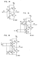
- Fig. 8 shows an inverter circuit of the fifth embodiment of this invention.
- the resistor 12 in the first embodiment shown in Fig. 3 is replaced by a second N-channel metal (silicon)-oxide-semiconductor field-effect transistor (hereinafter, referred simply as second NMOS and the NMOS 11 as first NMOS) 90.
- the second NMOS 90 has its gate G connected to the input end 16, and its drain D and source S connected to the drain D of the PMOS 10 and the base B of the second NPN 15, respectively.
- Like elements corresponding to those of Fig. 3 are identified by the same reference numerals.
- the operation of the inverter in Fig. 8 is substantially the same as in Fig. 3.
- the circuit of Fig. 8 is different from that of Fig. 3 in that when the first NPN 14 is turned off, or when the input terminal 16 is at "1" level, the second NMOS 90 is turned on, to discharge the charges accumulated in the first NPN 14.
- the source S of the second NMOS 90 is connected to the base B of the second NPN 15 so that the base current is increased to accelerate the switching of the second NPN 15 from the off-state to the on-state.
- the source S of the second NMOS 90 may be connected to the drain D of the first NMOS 11.
- the current is flowed through the resistor 12 when the PMOS 10 is switched from the off-state to the on-state, to delay the rise of the base potential of the first NPN 14, and thus to somewhat delay the switching of the first NPN 14 from the off-state to the on-state, but in this embodiment when the PMOS 10 is turned on from the off-state, the second NMOS 90 is turned off from the on-state so that no current flows between the drain D and source S of the NMOS 90.
- the base potential of the first NPN 14 rises faster than in the first embodiment, to accelerate the switching of the NPN 14 from the off- to the on-state.
- the second NMOS 90 is used in place of the resistor 12, so as to improve the density of integration and the operation speed, and the source S of the second NMOS 90 is connected to the base of the second NPN 15, so that the operation speed is further improved.
- Fig. 9 shows an inverter circuit of a sixth embodiment of this invention.
- the resistor 13 in the fifth embodiment of Fig. 8 is replaced by a P-channel junction field-effect transistor (hereinafter, referred to as PJFET) 100 as a second P-channel field effect transistor.
- PJFET P-channel junction field-effect transistor
- the gate of the PJFET 100 is connected to the input end 16 and the source and drain thereof are connected to the base and emitter of the second NPN 15, respectively.
- the embodiment of Fig. 9 is different from the fifth embodiment of Fig. 8 in that when the second NPN 15 is turned off from the on-state, or when the input terminal 16 is changed from level "1" to "0" level, the charges accumulated in the second NPN 15 are extracted through the PJFET 100. When the charges are discharged, the on-resistance of the PJFET 100 is decreased to accelerate the switching of the second NPN 15 from the on-state to the off-state. When the input terminal 16 changes from "0" to "1" level, the PJFET 100 is changed from the on-state to the off-state and thus the base current to the second NPN 15 is not shunted so that the second NPN 15 is rapidly turned on from the off-state.
- This embodiment has an effect for much higher speed.
- Fig. 10 shows an inverter circuit of a seventh embodiment of this invention.
- third NMOS 110 N-channel Metal-Oxide Semiconductor field-effect-transistor (hereinafter, referred to simply as third NMOS) 110.
- third NMOS 110 has its gate G connected to the base B of the first NPN 14, and its drain D and source S connected to the base B and emitter E of the second NPN 15, respectively.
- This embodiment is different from the fifth embodiment of Fig. 8 in that when the second NPN 15 is turned off from the on-state, or when the input terminal 16 is changed from "1" to "0" level, the charges accumulated in the second NPN 15 are extracted through the third NMOS 110.
- the high base potential of the first NPN 14 is applied to the gate of the third NMOS 110, which then turns on to form short circuit between the base and emitter of the second NPN 15, extracting the accumulated charges more rapidly.
- the present invention can be applied to output buffer circuits for driving an external circuit.
- the examples of such application are shown in Figs. 11, 12 and 13.
- the buffer circuit may be a multi-input NAND or multi-input NOR.
- Fig. 11 shows an inverting output circuit of an eighth embodiment of this invention. This circuit has substantially the same construction and similarly operates as the fifth embodiment of Fig. 8.
- Reference numeral 125 represents a first NPN with a Schottky barrier diode provided between the base and collector of the first NPN in Fig. 8 and so on, 126 a second NPN with a Schottky barrier diode provided between the base and collector of the second NPN, and 123 a fourth N-channel metal (silicon)-oxide-semiconductor field-effect-transistor (hereinafter, referred to simply as fourth NMOS) having its gate connected to the input terminal 16 and its drain D and source S respectively connected to the power supply terminal 1 and the base of the second NPN 126.
- fourth NMOS N-channel metal (silicon)-oxide-semiconductor field-effect-transistor
- This embodiment is different from the fifth embodiment 5 of Fig. 8 in that the first and second NPNs 125 and 126 have a Schottky barrier diode added, respectively, for the purpose of accelerating the time of extraction of accumulated charges, due to the saturation of the NPN transistors.
- this embodiment is different from the fifth embodiment of Fig. 8 in that the fourth NMOS 123 is provided between the power supply 1 and the base B of the second NPN 126, with its gate G being connected to the input terminal 16. This is because in the case of output circuit, a sink current I OL needs to be drawn in at a low-level output V OL and hence the second NPN 126 is required to be continuously supplied at its base with current at "1" level of the input terminal 16.
- a high-speed, low-power consumption inverting output circuit can be realized.
- Fig. 12 shows an inverting output circuit of a nineth embodiment of this invention. This circuit has substantially the same construction and similarly operates as the sixth embodiment in Fig. 9.
- Fig. 12 like elements corresponding to those of Figs. 9 and 11 are identified by the same reference numerals, and the resistor 13 in Fig. 11 is replaced by the PJFET 100 as in Fig. 9.
- This embodiment is different from Fig. 9 in that as in the eighth embodiment, the first and second NPN 125 and 126 have a Schottky barrier diode added, respectively, and that the fourth NMOS 123 is provided for supplying current to the base of the second NPN 126. According to this embodiment, a much higher-speed inverting output circuit can be realized.
- Fig. 13 shows an inverting output circuit of a tenth embodiment of this invention.
- This circuit has substantially the same construction and similarly operates as the seventh embodiment of Fig. 10.
- like elements corresponding to those of Figs. 10 and 11 are identified by the same reference numerals, and the resistor 13 in Fig. 11 is replaced by the third NMOS 110.
- This embodiment is different from Fig. 10 in that as in the eighth embodiment, the first and second NPN 125 and 126 have a Schottky barrier diode added and that the fourth NMOS 123 is provided for supplying current to the base of the second NPN 126. According to this embodiment, much higher density inverting output circuit can be realized.
- Fig. 14 shows an inverter circuit of an eleventh embodiment of this invention.
- reference numeral 114 represents a first PNP bipolar transistor (hereinafter, referred to simply as first PNP) having its emitter E connected to the power supply terminal 1 at which the first fixed potential is kept, and its collector connected to the output terminal 17.
- Numeral 115 denotes a send PNP bipolar transistor (hereinafter, referred to simply as second PNP) having its emitter E connected to the output terminal 17 and its collector C connected to ground potential GND at which the second fixed potential is maintained.
- the PMOS 10 has its gate G connected to the input terminal 16, and its source S and drain D respectively connected to the base B and collector C of the first PNP 114.
- the NM OS 11 has its gate G connected to the input terminal 16 and its drain D and source S respectively connected to the base B and collector C of the second PNP 115.
- the resistor 12 connects the drain D of the PMOS 10 and that of the NMOS 11.
- the resistor 13 connects the base B and emitter E of the first PNP 114.
- the NPN bipolar transistors 14 and 15 in the first embodiment are replaced by the PNP bipolar transistors 114 and 115, and the same operation as in the first embodiment is performed.
- Fig. 15 shows a two-input NAND circuit of a twelfth embodiment of this invention.
- reference numeral 326 represents a first PNP having its emitter E connected to the power supply terminal 1 and its collector connected to the output terminal 29, 327 a second PNP having its emitter E connected to the output terminal 29 and its collector C connected to the ground potential GND, 28 two input terminals, and 20 and 21 PMOSs having their gates G connected to one and the other of the input terminals 28, respectively and their source S-drain D paths connected in parallel between the base B and collector C of the first PNP 326.
- numerals 22 and 23 represent NMOSs having their gates G respectively connected to one and the other of the input terminals 28 and their drain D-source S paths connected in series between the base B and collector C of the second PNP 327, 24 a resistor connecting the drains D of the PMOSs 20 and 21 with the drain D of the NMOS 22, and 25 a resistor connecting the base B and emitter E of the first PNP 326.
- NPN bipolar transistors 26 and 27 in the second embodiment of Fig. 5 are respectively replaced by PNP bipolar transistors 326 and 327, and the same operation as in the second embodiment is performed.
- Fig. 16 shows a two-input NOR circuit of a thirteenth embodiment of this invention.
- reference numeral 436 represents a first PNP having its emitter E connected to the power supply 1 and its collector C connected to the output terminal 39, 437 a second PNP having its emitter E connected to the output terminal 39 and its collector C connected to the ground potential GND, 38 two input terminals, 30 and 31 PMOSs having their gates G connected to one and the other of the input terminals 38, respectively, and their source S-drain D paths connected in series between the base B and collector C of the first PNP 436, and 32 and 33 NMOSs having their gates G connected to one and the other of the input terminals 38, respectively and their drain D-source S paths connected in parallel between the base B and collector C of the second PNP 437.
- numeral 34 denotes a resistor connecting the drain D of the PMOS 31 with the drains of the NMOSs 32 and 33, and 35 a resistor connecting the base B and emitter E of the first PNP 436.
- the NPN bipolar transistors 36 and 37 in the third embodiment of Fig. 6 are replaced by the PNP bipolar transistors 436 and 437, respectively, and the same operation as in the third embodiment is performed.
- logic gates are only NAND and NOR circuits, it will easily be understood that other logic gate circuits such as AND and OR circuits, a combination logic circuit, flip-flops or shift registers can be formed by connecting a logic gate circuit of, for example, CMOS transistors to the input side of the NAND and NOR circuits.
Landscapes
- Engineering & Computer Science (AREA)
- Physics & Mathematics (AREA)
- Computer Hardware Design (AREA)
- Computing Systems (AREA)
- General Engineering & Computer Science (AREA)
- Mathematical Physics (AREA)
- Power Engineering (AREA)
- Condensed Matter Physics & Semiconductors (AREA)
- General Physics & Mathematics (AREA)
- Microelectronics & Electronic Packaging (AREA)
- Logic Circuits (AREA)
- Metal-Oxide And Bipolar Metal-Oxide Semiconductor Integrated Circuits (AREA)
Applications Claiming Priority (2)
| Application Number | Priority Date | Filing Date | Title |
|---|---|---|---|
| JP57119815A JPH0783252B2 (ja) | 1982-07-12 | 1982-07-12 | 半導体集積回路装置 |
| JP119815/82 | 1982-07-12 |
Related Child Applications (1)
| Application Number | Title | Priority Date | Filing Date |
|---|---|---|---|
| EP87118836.3 Division-Into | 1987-12-18 |
Publications (2)
| Publication Number | Publication Date |
|---|---|
| EP0099100A1 true EP0099100A1 (de) | 1984-01-25 |
| EP0099100B1 EP0099100B1 (de) | 1988-10-19 |
Family
ID=14770918
Family Applications (3)
| Application Number | Title | Priority Date | Filing Date |
|---|---|---|---|
| EP92122153A Withdrawn EP0543426A1 (de) | 1982-07-12 | 1983-07-11 | Gateschaltung mit Feldeffekt- und Bipolartransistoren |
| EP83106796A Expired EP0099100B1 (de) | 1982-07-12 | 1983-07-11 | Gateschaltung mit Feldeffekt- und Bipolartransistoren |
| EP87118836A Expired - Lifetime EP0279943B1 (de) | 1982-07-12 | 1983-07-11 | Torschaltung mit Feldeffekt- und Bipolartransistoren |
Family Applications Before (1)
| Application Number | Title | Priority Date | Filing Date |
|---|---|---|---|
| EP92122153A Withdrawn EP0543426A1 (de) | 1982-07-12 | 1983-07-11 | Gateschaltung mit Feldeffekt- und Bipolartransistoren |
Family Applications After (1)
| Application Number | Title | Priority Date | Filing Date |
|---|---|---|---|
| EP87118836A Expired - Lifetime EP0279943B1 (de) | 1982-07-12 | 1983-07-11 | Torschaltung mit Feldeffekt- und Bipolartransistoren |
Country Status (5)
| Country | Link |
|---|---|
| US (4) | US4719373A (de) |
| EP (3) | EP0543426A1 (de) |
| JP (1) | JPH0783252B2 (de) |
| KR (1) | KR920004919B1 (de) |
| DE (2) | DE3378291D1 (de) |
Cited By (37)
| Publication number | Priority date | Publication date | Assignee | Title |
|---|---|---|---|---|
| DE3403276A1 (de) * | 1983-01-31 | 1984-08-02 | Hitachi, Ltd., Tokio/Tokyo | Integrierte halbleiterschaltung |
| EP0132822A2 (de) * | 1983-07-25 | 1985-02-13 | Hitachi, Ltd. | Zusammengesetzte Schaltung aus bipolaren und Feldeffekt-Transistoren |
| EP0134731A1 (de) * | 1983-07-08 | 1985-03-20 | Fujitsu Limited | Integrierte Komplementärlogikschaltung |
| EP0145004A2 (de) * | 1983-12-12 | 1985-06-19 | Hitachi, Ltd. | Kombinierte Bipolartransistor-Feldeffekttransistor-Schaltung |
| DE3504930A1 (de) * | 1984-02-13 | 1985-08-14 | Hitachi, Ltd., Tokio/Tokyo | Integrierte halbleiterschaltung |
| DE3510948A1 (de) * | 1984-03-26 | 1985-10-03 | Hitachi, Ltd., Tokio/Tokyo | Schaltungsvorrichtung |
| GB2156614A (en) * | 1984-02-24 | 1985-10-09 | Hitachi Ltd | A switching circuit |
| US4612458A (en) * | 1985-08-28 | 1986-09-16 | Advanced Micro Devices, Inc. | Merged PMOS/bipolar logic circuits |
| EP0196113A2 (de) * | 1985-03-29 | 1986-10-01 | Kabushiki Kaisha Toshiba | Tri-state-Pufferschaltung |
| US4616146A (en) * | 1984-09-04 | 1986-10-07 | Motorola, Inc. | BI-CMOS driver circuit |
| US4647794A (en) * | 1985-05-22 | 1987-03-03 | Teledyne Industries, Inc. | Solid state relay having non overlapping switch closures |
| EP0212004A2 (de) * | 1985-07-01 | 1987-03-04 | Kabushiki Kaisha Toshiba | Halbleiter-Inverterschaltung mit Bipolartransistor zur schnellen Verarbeitung von Ein-/Ausgangssignalen |
| US4649294A (en) * | 1986-01-13 | 1987-03-10 | Motorola, Inc. | BIMOS logic gate |
| EP0225489A2 (de) * | 1985-11-13 | 1987-06-16 | Nec Corporation | Logischer Schaltkreis |
| US4678940A (en) * | 1986-01-08 | 1987-07-07 | Advanced Micro Devices, Inc. | TTL compatible merged bipolar/CMOS output buffer circuits |
| EP0239059A2 (de) * | 1986-03-22 | 1987-09-30 | Kabushiki Kaisha Toshiba | Logische Schaltung |
| US4701642A (en) * | 1986-04-28 | 1987-10-20 | International Business Machines Corporation | BICMOS binary logic circuits |
| EP0250947A2 (de) * | 1986-06-27 | 1988-01-07 | Motorola, Inc. | Logisches Tor vom Bimos-Typ |
| EP0261528A1 (de) * | 1986-09-26 | 1988-03-30 | Kabushiki Kaisha Toshiba | Logische Schaltung |
| US4746817A (en) * | 1987-03-16 | 1988-05-24 | International Business Machines Corporation | BIFET logic circuit |
| US4791320A (en) * | 1985-08-20 | 1988-12-13 | Fujitsu Limited | Bipolar-MISFET compound inverter with discharge transistor |
| US4827368A (en) * | 1985-03-25 | 1989-05-02 | Hitachi, Ltd. | Semiconductor integrated circuit device |
| US4849658A (en) * | 1986-08-08 | 1989-07-18 | Hitachi, Ltd. | Dynamic logic circuit including bipolar transistors and field-effect transistors |
| EP0152939A3 (en) * | 1984-02-20 | 1989-07-19 | Hitachi, Ltd. | Arithmetic operation unit and arithmetic operation circuit |
| GB2217941A (en) * | 1988-04-21 | 1989-11-01 | Samsung Electronics Co Ltd | Bicmos inverter circuit |
| US4880998A (en) * | 1987-09-08 | 1989-11-14 | Mitsubishi Denki Kabushiki Kaisha | Bipolar transistor and CMOS transistor logic circuit having improved discharge capabilities |
| EP0375979A2 (de) * | 1988-12-27 | 1990-07-04 | International Business Machines Corporation | BICMOS-Treiberschaltung für CMOS-logische Schaltungen hoher Dichte |
| US4965470A (en) * | 1989-01-30 | 1990-10-23 | Samsung Electronics Co., Ltd. | High integrated Bi-CMOS logic circuit |
| EP0398744A2 (de) * | 1989-05-19 | 1990-11-22 | Fujitsu Limited | Bi-CMOS-Logikschaltung |
| EP0431893A2 (de) * | 1989-12-05 | 1991-06-12 | Hewlett-Packard Company | BICMOS-Logikgatterschaltung und Strukturen |
| EP0441317A1 (de) * | 1990-02-07 | 1991-08-14 | Kabushiki Kaisha Toshiba | Bi-CMOS logischer Gatterschaltkreis für integrierte Niederspannungshalbleiterschaltkreise |
| EP0452919A2 (de) * | 1990-04-20 | 1991-10-23 | Kabushiki Kaisha Toshiba | Bi-MOS-integrierte logische Schaltung |
| US5138195A (en) * | 1989-05-19 | 1992-08-11 | Fujitsu Limited | Bi-CMOS logic circuit having full voltage swing and rapid turn-off |
| EP0588784A1 (de) * | 1992-09-17 | 1994-03-23 | Austria Mikro Systeme International Aktiengesellschaft | Integrierte BICMOS-Schaltungsanordnung |
| US5378941A (en) * | 1983-04-15 | 1995-01-03 | Hitachi, Ltd. | Bipolar transistor MOS transistor hybrid semiconductor integrated circuit device |
| EP0645890A2 (de) * | 1993-09-24 | 1995-03-29 | Nec Corporation | BICMOS-Logikschaltung |
| EP0533354B1 (de) * | 1991-09-18 | 1999-02-03 | STMicroelectronics, Inc. | Treiberschaltung mit FET und bipolaren Transistoren |
Families Citing this family (58)
| Publication number | Priority date | Publication date | Assignee | Title |
|---|---|---|---|---|
| JPH0783252B2 (ja) * | 1982-07-12 | 1995-09-06 | 株式会社日立製作所 | 半導体集積回路装置 |
| US5239212A (en) * | 1982-07-12 | 1993-08-24 | Hitachi, Ltd. | Gate circuit of combined field-effect and bipolar transistors with an improved discharge arrangement |
| JPS5994861A (ja) * | 1982-11-24 | 1984-05-31 | Hitachi Ltd | 半導体集積回路装置及びその製造方法 |
| JPS60194615A (ja) * | 1984-03-16 | 1985-10-03 | Hitachi Ltd | 複合出力回路 |
| JPS613390A (ja) * | 1984-06-15 | 1986-01-09 | Hitachi Ltd | 記憶装置 |
| JP2552107B2 (ja) * | 1985-01-14 | 1996-11-06 | 日本電信電話株式会社 | 同期式複合型集積回路装置 |
| EP0349022A3 (de) * | 1985-01-30 | 1991-07-24 | Kabushiki Kaisha Toshiba | Halbleiteranordnung |
| JPS61245625A (ja) * | 1985-04-24 | 1986-10-31 | Hitachi Ltd | 半導体集積回路装置 |
| JPS63164612A (ja) * | 1986-12-26 | 1988-07-08 | Hitachi Ltd | 演算回路 |
| JPS63209220A (ja) * | 1987-02-26 | 1988-08-30 | Toshiba Corp | インバ−タ回路 |
| JPH0611111B2 (ja) * | 1987-03-27 | 1994-02-09 | 株式会社東芝 | BiMOS論理回路 |
| KR900001062B1 (ko) * | 1987-09-15 | 1990-02-26 | 강진구 | 반도체 바이 씨 모오스 장치의 제조방법 |
| JPH0611112B2 (ja) * | 1987-11-28 | 1994-02-09 | 株式会社東芝 | 出力回路 |
| JP2550138B2 (ja) * | 1988-03-18 | 1996-11-06 | 株式会社日立製作所 | バイポーラトランジスタと電界効果トランジスタとを有する半導体集積回路装置 |
| US5187615A (en) * | 1988-03-30 | 1993-02-16 | Hitachi, Ltd. | Data separator and signal processing circuit |
| JPH0239719A (ja) * | 1988-07-29 | 1990-02-08 | Fujitsu Ltd | 半導体回路 |
| US5068553A (en) * | 1988-10-31 | 1991-11-26 | Texas Instruments Incorporated | Delay stage with reduced Vdd dependence |
| JPH02143711A (ja) * | 1988-11-25 | 1990-06-01 | Nec Corp | トランジスタ回路 |
| US4980578A (en) * | 1988-12-20 | 1990-12-25 | Texas Instruments Incorporated | Fast sense amplifier |
| JPH0736507B2 (ja) * | 1989-02-02 | 1995-04-19 | 株式会社東芝 | 半導体論理回路 |
| EP0404025B1 (de) * | 1989-06-19 | 1995-04-05 | Heimann Optoelectronics GmbH | Schaltungsanordnung zur Ansteuerung von Schaltelementen, die insbesondere geeignet ist für Flüssigkristallbildschirme |
| US5107141A (en) * | 1989-11-01 | 1992-04-21 | Hitachi, Ltd. | BiCMOS logic circuit using 0.5 micron technology and having an operating potential difference of less than 4 volts |
| JP2820980B2 (ja) * | 1989-11-02 | 1998-11-05 | 富士通株式会社 | 論理回路 |
| KR920010212B1 (ko) * | 1989-12-29 | 1992-11-21 | 삼성전자 주식회사 | 바이씨모스 ttl레벨 출력구동회로 |
| JP2546904B2 (ja) * | 1990-01-31 | 1996-10-23 | 三菱電機株式会社 | 半導体論理回路 |
| US5182472A (en) * | 1990-02-08 | 1993-01-26 | Nec Corporation | Logic circuit with bipolar CMOS configuration |
| US5121013A (en) * | 1990-02-12 | 1992-06-09 | Advanced Micro Devices, Inc. | Noise reducing output buffer circuit with feedback path |
| JP2661318B2 (ja) * | 1990-03-27 | 1997-10-08 | 日本電気株式会社 | 半導体装置 |
| JP2623918B2 (ja) * | 1990-06-04 | 1997-06-25 | 日本電気株式会社 | 出力バッファ回路 |
| JPH0440014A (ja) * | 1990-06-05 | 1992-02-10 | Mitsubishi Electric Corp | 論理回路装置 |
| US5241221A (en) * | 1990-07-06 | 1993-08-31 | North American Philips Corp., Signetics Div. | CMOS driver circuit having reduced switching noise |
| US5111076A (en) * | 1990-09-05 | 1992-05-05 | Min Ming Tarng | Digital superbuffer |
| JP3028840B2 (ja) * | 1990-09-19 | 2000-04-04 | 株式会社日立製作所 | バイポーラトランジスタとmosトランジスタの複合回路、及びそれを用いた半導体集積回路装置 |
| JP2607394B2 (ja) * | 1990-11-01 | 1997-05-07 | 株式会社日立製作所 | 非反転バッファ装置および半導体記憶装置 |
| ES2091303T3 (es) * | 1990-11-30 | 1996-11-01 | Canon Kk | Cabezal para impresion por chorros de tinta y circuito de control para el mismo. |
| US5153464A (en) * | 1990-12-14 | 1992-10-06 | Hewlett-Packard Company | Bicmos tri-state output buffer |
| US5128562A (en) * | 1990-12-19 | 1992-07-07 | North American Philips Corporation, Signetics Division | Memory element with high metastability-immunity |
| JPH0697804A (ja) * | 1991-01-08 | 1994-04-08 | Nec Corp | 論理回路 |
| JP3079515B2 (ja) * | 1991-01-29 | 2000-08-21 | 株式会社東芝 | ゲ−トアレイ装置及び入力回路及び出力回路及び降圧回路 |
| US5132567A (en) * | 1991-04-18 | 1992-07-21 | International Business Machines Corporation | Low threshold BiCMOS circuit |
| US5191240A (en) * | 1991-06-05 | 1993-03-02 | International Business Machines Corporation | Bicmos driver circuits with improved low output level |
| US5118972A (en) * | 1991-06-13 | 1992-06-02 | International Business Machines Corporation | BiCMOS gate pull-down circuit |
| US5994755A (en) | 1991-10-30 | 1999-11-30 | Intersil Corporation | Analog-to-digital converter and method of fabrication |
| US5369309A (en) * | 1991-10-30 | 1994-11-29 | Harris Corporation | Analog-to-digital converter and method of fabrication |
| US5243237A (en) * | 1992-01-22 | 1993-09-07 | Samsung Semiconductor, Inc. | Noninverting bi-cmos gates with propagation delays of a single bi-cmos inverter |
| EP0565807A1 (de) * | 1992-04-17 | 1993-10-20 | STMicroelectronics S.r.l. | MOS-Leistungstransistorbauelement |
| US5376816A (en) * | 1992-06-24 | 1994-12-27 | Nec Corporation | Bi-cmos integrated circuit device having buried region use in common for bipolar and mos transistors |
| JP2937652B2 (ja) * | 1992-10-01 | 1999-08-23 | 日本電気株式会社 | BiMIS論理回路 |
| US5355030A (en) * | 1992-12-04 | 1994-10-11 | International Business Machines Corporation | Low voltage BICMOS logic switching circuit |
| US5430408A (en) * | 1993-03-08 | 1995-07-04 | Texas Instruments Incorporated | Transmission gate circuit |
| US5886542A (en) * | 1993-08-18 | 1999-03-23 | Texas Instruments Incorporated | Quasi-complementary BiCMOS circuit with enhanced pull down transistor clamp |
| JP2727952B2 (ja) * | 1994-02-14 | 1998-03-18 | 株式会社日立製作所 | 半導体集積回路装置 |
| US5576654A (en) * | 1995-05-16 | 1996-11-19 | Harris Corporation | BIMOS driver circuit and method |
| JP2600635B2 (ja) * | 1995-07-10 | 1997-04-16 | 株式会社日立製作所 | 3ステート回路 |
| JP2800734B2 (ja) * | 1995-09-06 | 1998-09-21 | 日本電気株式会社 | 半導体集積回路 |
| US20040003828A1 (en) * | 2002-03-21 | 2004-01-08 | Jackson David P. | Precision surface treatments using dense fluids and a plasma |
| CN100442513C (zh) | 2002-11-29 | 2008-12-10 | 株式会社东芝 | 半导体集成电路装置及使用它的电子卡 |
| US7656224B2 (en) * | 2005-03-16 | 2010-02-02 | Texas Instruments Incorporated | Power efficient dynamically biased buffer for low drop out regulators |
Citations (3)
| Publication number | Priority date | Publication date | Assignee | Title |
|---|---|---|---|---|
| US3541353A (en) * | 1967-09-13 | 1970-11-17 | Motorola Inc | Mosfet digital gate |
| DE2148891A1 (de) * | 1971-09-30 | 1973-04-05 | Siemens Ag | Schaltungsanordnung zum umschalten der stromrichtung in einem verbraucher |
| US4122360A (en) * | 1976-08-03 | 1978-10-24 | Tokyo Shibaura Electric Company, Limited | Logic circuit using CMOS transistors |
Family Cites Families (21)
| Publication number | Priority date | Publication date | Assignee | Title |
|---|---|---|---|---|
| US425877A (en) * | 1890-04-15 | Process of carbureting air or gas | ||
| US3370995A (en) * | 1965-08-02 | 1968-02-27 | Texas Instruments Inc | Method for fabricating electrically isolated semiconductor devices in integrated circuits |
| USRE27804E (en) * | 1967-02-28 | 1973-10-30 | Transistor-transistor logic circuits having improved voltage transfer characteristics | |
| BE793033A (fr) * | 1971-12-22 | 1973-04-16 | Owens Illinois Inc | Generateur de tension d'entretien a verrouillage de baker pour panneauxd'indication a decharges pulsees |
| US3831102A (en) * | 1973-03-09 | 1974-08-20 | Rauland Corp | Push-pull audio amplifier |
| US3930169A (en) * | 1973-09-27 | 1975-12-30 | Motorola Inc | Cmos odd multiple repetition rate divider circuit |
| US3867644A (en) * | 1974-01-07 | 1975-02-18 | Signetics Corp | High speed low power schottky integrated logic gate circuit with current boost |
| DE2461935A1 (de) * | 1974-01-10 | 1975-07-17 | Hughes Aircraft Co | Flipflop |
| US4132906A (en) * | 1977-02-28 | 1979-01-02 | Motorola, Inc. | Circuit to improve rise time and/or reduce parasitic power supply spike current in bipolar transistor logic circuits |
| US4103188A (en) * | 1977-08-22 | 1978-07-25 | Rca Corporation | Complementary-symmetry amplifier |
| JPS5846863B2 (ja) * | 1977-08-25 | 1983-10-19 | 松下電器産業株式会社 | 半導体集積回路装置 |
| JPS5545207A (en) * | 1978-09-26 | 1980-03-29 | Oki Electric Ind Co Ltd | Complementary mos inverter circuit unit and its production |
| JPS5553910A (en) * | 1978-10-16 | 1980-04-19 | Nec Corp | Power amplifier |
| US4325180A (en) * | 1979-02-15 | 1982-04-20 | Texas Instruments Incorporated | Process for monolithic integration of logic, control, and high voltage interface circuitry |
| US4301383A (en) * | 1979-10-05 | 1981-11-17 | Harris Corporation | Complementary IGFET buffer with improved bipolar output |
| JPS5693428A (en) * | 1979-12-10 | 1981-07-29 | Reliance Electric Co | High voltage and large current solid state switching circuit |
| JPS56100461A (en) * | 1980-01-17 | 1981-08-12 | Nippon Telegr & Teleph Corp <Ntt> | Semiconductor ic device |
| US4512815A (en) * | 1980-05-27 | 1985-04-23 | National Semiconductor Corporation | Simplified BIFET process |
| US4356416A (en) * | 1980-07-17 | 1982-10-26 | General Electric Company | Voltage controlled non-saturating semiconductor switch and voltage converter circuit employing same |
| JPH0783252B2 (ja) * | 1982-07-12 | 1995-09-06 | 株式会社日立製作所 | 半導体集積回路装置 |
| US4616146A (en) * | 1984-09-04 | 1986-10-07 | Motorola, Inc. | BI-CMOS driver circuit |
-
1982
- 1982-07-12 JP JP57119815A patent/JPH0783252B2/ja not_active Expired - Lifetime
-
1983
- 1983-07-11 EP EP92122153A patent/EP0543426A1/de not_active Withdrawn
- 1983-07-11 DE DE8383106796T patent/DE3378291D1/de not_active Expired
- 1983-07-11 DE DE87118836T patent/DE3382717T2/de not_active Expired - Fee Related
- 1983-07-11 EP EP83106796A patent/EP0099100B1/de not_active Expired
- 1983-07-11 EP EP87118836A patent/EP0279943B1/de not_active Expired - Lifetime
- 1983-07-12 KR KR1019830003180A patent/KR920004919B1/ko not_active IP Right Cessation
-
1987
- 1987-04-30 US US07/045,216 patent/US4719373A/en not_active Expired - Lifetime
- 1987-12-01 US US07/127,183 patent/US4829201A/en not_active Expired - Lifetime
- 1987-12-01 US US07/127,206 patent/US5001366A/en not_active Expired - Lifetime
- 1987-12-01 US US07/127,184 patent/US4890017A/en not_active Expired - Lifetime
Patent Citations (3)
| Publication number | Priority date | Publication date | Assignee | Title |
|---|---|---|---|---|
| US3541353A (en) * | 1967-09-13 | 1970-11-17 | Motorola Inc | Mosfet digital gate |
| DE2148891A1 (de) * | 1971-09-30 | 1973-04-05 | Siemens Ag | Schaltungsanordnung zum umschalten der stromrichtung in einem verbraucher |
| US4122360A (en) * | 1976-08-03 | 1978-10-24 | Tokyo Shibaura Electric Company, Limited | Logic circuit using CMOS transistors |
Non-Patent Citations (6)
| Title |
|---|
| IBM TECHNICAL DISCLOSURE BULLETIN, vol. 16, no. 11, April 1974 W.B. CHIN "Push-pull driver using bipolar and complementary metal-oxide semiconductor devices", pages 3570, 3571 * Figure, elements Q2, Q3, P1, N1 * * |
| Patent Abstracts of Japan vol. 2, no. 120, 6 October 1978 page 6968E78 & JP-A-53 086151 * |
| Patent Abstracts of Japan vol. 4, no. 1, 8 January 1980 page 116E163 & JP-A-54 142061 * |
| Patent Abstracts of Japan vol. 4, no. 59, 2 May 1980 page 9E9 & JP-A-55 027790 * |
| Patent Abstracts of Japan vol. 4, no. 79, 7 June 1980 page 27E14 & JP-A-55 045259 * |
| Patent Abstracts of Japan vol. 4, no. 8, 22 January 1980 page 103E166 & JP-A-54 148469 * |
Cited By (74)
| Publication number | Priority date | Publication date | Assignee | Title |
|---|---|---|---|---|
| DE3448428C2 (de) * | 1983-01-31 | 1992-09-10 | Hitachi, Ltd., Tokio/Tokyo, Jp | |
| DE3448427C2 (de) * | 1983-01-31 | 1992-10-15 | Hitachi, Ltd., Tokio/Tokyo, Jp | |
| DE3448455C2 (de) * | 1983-01-31 | 1993-07-01 | Hitachi, Ltd., Tokio/Tokyo, Jp | |
| DE3403276A1 (de) * | 1983-01-31 | 1984-08-02 | Hitachi, Ltd., Tokio/Tokyo | Integrierte halbleiterschaltung |
| DE3448435C2 (de) * | 1983-01-31 | 1993-08-19 | Hitachi, Ltd., Tokio/Tokyo, Jp | |
| US5378941A (en) * | 1983-04-15 | 1995-01-03 | Hitachi, Ltd. | Bipolar transistor MOS transistor hybrid semiconductor integrated circuit device |
| EP0134731A1 (de) * | 1983-07-08 | 1985-03-20 | Fujitsu Limited | Integrierte Komplementärlogikschaltung |
| US4816705A (en) * | 1983-07-08 | 1989-03-28 | Fujitsu Limited | Bi-CMOS logic circuit |
| EP0132822A3 (en) * | 1983-07-25 | 1987-02-04 | Hitachi, Ltd. | Composite circuit of bipolar transistors and field effect transistors |
| EP0132822A2 (de) * | 1983-07-25 | 1985-02-13 | Hitachi, Ltd. | Zusammengesetzte Schaltung aus bipolaren und Feldeffekt-Transistoren |
| US4808850A (en) * | 1983-07-25 | 1989-02-28 | Hitachi, Ltd. | Composite circuit of bipolar transistors and field effect transistors |
| US4661723A (en) * | 1983-07-25 | 1987-04-28 | Hitachi, Ltd. | Composite circuit of bipolar transistors and field effect transistors |
| EP0145004A2 (de) * | 1983-12-12 | 1985-06-19 | Hitachi, Ltd. | Kombinierte Bipolartransistor-Feldeffekttransistor-Schaltung |
| US4769561A (en) * | 1983-12-12 | 1988-09-06 | Hitachi, Ltd. | Bipolar transistor-field effect transistor composite circuit |
| EP0145004A3 (en) * | 1983-12-12 | 1987-08-19 | Hitachi, Ltd. | Bipolar transistor-field effect transistor composite circuit |
| GB2156616A (en) * | 1984-02-13 | 1985-10-09 | Hitachi Ltd | A semiconductor integrated circuit |
| DE3504930A1 (de) * | 1984-02-13 | 1985-08-14 | Hitachi, Ltd., Tokio/Tokyo | Integrierte halbleiterschaltung |
| US4713796A (en) * | 1984-02-13 | 1987-12-15 | Hitachi, Ltd. | Semiconductor integrated circuit |
| US5311482A (en) * | 1984-02-13 | 1994-05-10 | Hitachi, Ltd. | Semiconductor integrated circuit |
| EP0152939A3 (en) * | 1984-02-20 | 1989-07-19 | Hitachi, Ltd. | Arithmetic operation unit and arithmetic operation circuit |
| GB2156614A (en) * | 1984-02-24 | 1985-10-09 | Hitachi Ltd | A switching circuit |
| US4678943A (en) * | 1984-02-24 | 1987-07-07 | Hitachi, Ltd. | Inverting logic buffer BICMOS switching circuit using an enabling switch for three-state operation with reduced dissipation |
| DE3510948A1 (de) * | 1984-03-26 | 1985-10-03 | Hitachi, Ltd., Tokio/Tokyo | Schaltungsvorrichtung |
| GB2158313A (en) * | 1984-03-26 | 1985-11-06 | Hitachi Ltd | A switching circuit |
| US4616146A (en) * | 1984-09-04 | 1986-10-07 | Motorola, Inc. | BI-CMOS driver circuit |
| US4827368A (en) * | 1985-03-25 | 1989-05-02 | Hitachi, Ltd. | Semiconductor integrated circuit device |
| US4725982A (en) * | 1985-03-29 | 1988-02-16 | Kabushiki Kaisha Toshiba | Tri-state buffer circuit |
| EP0196113A3 (en) * | 1985-03-29 | 1987-09-02 | Kabushiki Kaisha Toshiba | Tri-state buffer circuit |
| EP0196113A2 (de) * | 1985-03-29 | 1986-10-01 | Kabushiki Kaisha Toshiba | Tri-state-Pufferschaltung |
| US4647794A (en) * | 1985-05-22 | 1987-03-03 | Teledyne Industries, Inc. | Solid state relay having non overlapping switch closures |
| EP0212004A3 (en) * | 1985-07-01 | 1987-10-28 | Kabushiki Kaisha Toshiba | A solid state inverting circuit having a bipolar transistor for rapidly processing i/o signals |
| EP0212004A2 (de) * | 1985-07-01 | 1987-03-04 | Kabushiki Kaisha Toshiba | Halbleiter-Inverterschaltung mit Bipolartransistor zur schnellen Verarbeitung von Ein-/Ausgangssignalen |
| US4791320A (en) * | 1985-08-20 | 1988-12-13 | Fujitsu Limited | Bipolar-MISFET compound inverter with discharge transistor |
| US4612458A (en) * | 1985-08-28 | 1986-09-16 | Advanced Micro Devices, Inc. | Merged PMOS/bipolar logic circuits |
| EP0225489A3 (de) * | 1985-11-13 | 1987-10-28 | Nec Corporation | Logischer Schaltkreis |
| EP0225489A2 (de) * | 1985-11-13 | 1987-06-16 | Nec Corporation | Logischer Schaltkreis |
| EP0231667A2 (de) * | 1986-01-08 | 1987-08-12 | Advanced Micro Devices, Inc. | Ausgangspufferschaltungen |
| US4678940A (en) * | 1986-01-08 | 1987-07-07 | Advanced Micro Devices, Inc. | TTL compatible merged bipolar/CMOS output buffer circuits |
| EP0231667A3 (de) * | 1986-01-08 | 1989-02-22 | Advanced Micro Devices, Inc. | Ausgangspufferschaltungen |
| US4649294A (en) * | 1986-01-13 | 1987-03-10 | Motorola, Inc. | BIMOS logic gate |
| EP0239059A2 (de) * | 1986-03-22 | 1987-09-30 | Kabushiki Kaisha Toshiba | Logische Schaltung |
| EP0239059A3 (en) * | 1986-03-22 | 1988-02-03 | Kabushiki Kaisha Toshiba | Logical circuit |
| EP0243603A3 (en) * | 1986-04-28 | 1989-03-15 | International Business Machines Corporation | Binary logic circuit |
| EP0243603A2 (de) * | 1986-04-28 | 1987-11-04 | International Business Machines Corporation | Binäre logische Schaltung |
| US4701642A (en) * | 1986-04-28 | 1987-10-20 | International Business Machines Corporation | BICMOS binary logic circuits |
| EP0250947A3 (de) * | 1986-06-27 | 1989-04-19 | Motorola, Inc. | Logisches Tor vom Bimos-Typ |
| EP0250947A2 (de) * | 1986-06-27 | 1988-01-07 | Motorola, Inc. | Logisches Tor vom Bimos-Typ |
| US4849658A (en) * | 1986-08-08 | 1989-07-18 | Hitachi, Ltd. | Dynamic logic circuit including bipolar transistors and field-effect transistors |
| US4779014A (en) * | 1986-09-26 | 1988-10-18 | Kabushiki Kaisha Toshiba | BiCMOS logic circuit with additional drive to the pull-down bipolar output transistor |
| EP0261528A1 (de) * | 1986-09-26 | 1988-03-30 | Kabushiki Kaisha Toshiba | Logische Schaltung |
| EP0282702A2 (de) * | 1987-03-16 | 1988-09-21 | International Business Machines Corporation | BIFET-Logik-Schaltung |
| EP0282702A3 (en) * | 1987-03-16 | 1989-07-12 | International Business Machines Corporation | Bifet logic circuit |
| US4746817A (en) * | 1987-03-16 | 1988-05-24 | International Business Machines Corporation | BIFET logic circuit |
| US4880998A (en) * | 1987-09-08 | 1989-11-14 | Mitsubishi Denki Kabushiki Kaisha | Bipolar transistor and CMOS transistor logic circuit having improved discharge capabilities |
| GB2217941A (en) * | 1988-04-21 | 1989-11-01 | Samsung Electronics Co Ltd | Bicmos inverter circuit |
| GB2217941B (en) * | 1988-04-21 | 1992-01-29 | Samsung Electronics Co Ltd | Bicmos inverter circuit |
| EP0375979A3 (en) * | 1988-12-27 | 1990-09-12 | International Business Machines Corporation | Bicmos driver circuit for high density cmos logic circuits |
| EP0375979A2 (de) * | 1988-12-27 | 1990-07-04 | International Business Machines Corporation | BICMOS-Treiberschaltung für CMOS-logische Schaltungen hoher Dichte |
| US4965470A (en) * | 1989-01-30 | 1990-10-23 | Samsung Electronics Co., Ltd. | High integrated Bi-CMOS logic circuit |
| EP0398744A3 (de) * | 1989-05-19 | 1991-04-17 | Fujitsu Limited | Bi-CMOS-Logikschaltung |
| US5097150A (en) * | 1989-05-19 | 1992-03-17 | Fujitsu Limited | Bi-cmos logic circuit |
| US5138195A (en) * | 1989-05-19 | 1992-08-11 | Fujitsu Limited | Bi-CMOS logic circuit having full voltage swing and rapid turn-off |
| EP0398744A2 (de) * | 1989-05-19 | 1990-11-22 | Fujitsu Limited | Bi-CMOS-Logikschaltung |
| EP0431893A3 (en) * | 1989-12-05 | 1992-02-12 | Hewlett-Packard Company | Novel bicmos logic gate circuit and structures |
| EP0431893A2 (de) * | 1989-12-05 | 1991-06-12 | Hewlett-Packard Company | BICMOS-Logikgatterschaltung und Strukturen |
| EP0441317A1 (de) * | 1990-02-07 | 1991-08-14 | Kabushiki Kaisha Toshiba | Bi-CMOS logischer Gatterschaltkreis für integrierte Niederspannungshalbleiterschaltkreise |
| US5146118A (en) * | 1990-02-07 | 1992-09-08 | Kabushiki Kaisha Toshiba | Bi-cmos logic gate circuits for low-voltage semiconductor integrated circuits |
| EP0452919A3 (en) * | 1990-04-20 | 1991-11-13 | Kabushiki Kaisha Toshiba | Bi-mos semiconductor integrated circuit |
| EP0452919A2 (de) * | 1990-04-20 | 1991-10-23 | Kabushiki Kaisha Toshiba | Bi-MOS-integrierte logische Schaltung |
| EP0533354B1 (de) * | 1991-09-18 | 1999-02-03 | STMicroelectronics, Inc. | Treiberschaltung mit FET und bipolaren Transistoren |
| EP0588784A1 (de) * | 1992-09-17 | 1994-03-23 | Austria Mikro Systeme International Aktiengesellschaft | Integrierte BICMOS-Schaltungsanordnung |
| AT404078B (de) * | 1992-09-17 | 1998-08-25 | Austria Mikrosysteme Int | Integrierte bicmos-schaltungsanordnung |
| EP0645890A2 (de) * | 1993-09-24 | 1995-03-29 | Nec Corporation | BICMOS-Logikschaltung |
| EP0645890B1 (de) * | 1993-09-24 | 2001-12-12 | Nec Corporation | BICMOS-Logikschaltung |
Also Published As
| Publication number | Publication date |
|---|---|
| KR840005629A (ko) | 1984-11-14 |
| EP0279943A1 (de) | 1988-08-31 |
| DE3382717D1 (de) | 1993-11-11 |
| EP0543426A1 (de) | 1993-05-26 |
| US4829201A (en) | 1989-05-09 |
| DE3382717T2 (de) | 1994-05-05 |
| EP0099100B1 (de) | 1988-10-19 |
| DE3378291D1 (en) | 1988-11-24 |
| JPH0783252B2 (ja) | 1995-09-06 |
| US4890017A (en) | 1989-12-26 |
| US5001366A (en) | 1991-03-19 |
| JPS5911034A (ja) | 1984-01-20 |
| KR920004919B1 (ko) | 1992-06-22 |
| EP0279943B1 (de) | 1993-10-06 |
| US4719373A (en) | 1988-01-12 |
Similar Documents
| Publication | Publication Date | Title |
|---|---|---|
| US4829201A (en) | Gate circuit of combined field-effect and bipolar transistors | |
| EP0145004B1 (de) | Kombinierte Bipolartransistor-Feldeffekttransistor-Schaltung | |
| US4808850A (en) | Composite circuit of bipolar transistors and field effect transistors | |
| JPH0616585B2 (ja) | バツフア回路 | |
| EP0267361A1 (de) | CMOS-Treiberschaltung mit hoher Schaltgeschwindigkeit | |
| US4725982A (en) | Tri-state buffer circuit | |
| JPH0583004B2 (de) | ||
| EP0417786A2 (de) | Pegelverschiebeschaltung zum Erzielen einer Hochgeschwindigkeits-Verarbeitung und einer verbesserten Ausgangsstrom-Speisefähigkeit | |
| US5057713A (en) | Bipolar MOS logic circuit and semiconductor integrated circuit | |
| US5239212A (en) | Gate circuit of combined field-effect and bipolar transistors with an improved discharge arrangement | |
| US5118972A (en) | BiCMOS gate pull-down circuit | |
| US5124582A (en) | Bi-cmos circuit with high-speed active pull-down output currents | |
| US5057714A (en) | BiCMOS integrated circuit device utilizing Schottky diodes | |
| JPH0337767B2 (de) | ||
| US5600268A (en) | Gate circuit of combined field-effect and bipolar transistors | |
| EP0735686A1 (de) | CMOS Ausgangspuffer mit drei Zuständen | |
| JP3190191B2 (ja) | 出力バッファ回路 | |
| KR950000352B1 (ko) | 반도체 논리회로 | |
| JPH1028045A (ja) | Mosトランジスタ回路 | |
| JPS6232722A (ja) | プツシユプル出力回路 | |
| US6329844B2 (en) | Semiconductor integrated circuit | |
| JP2549185B2 (ja) | 半導体集積回路装置 | |
| JPH0613868A (ja) | バイ−cmos出力回路 | |
| JPS6094740A (ja) | マスタ−スライスic | |
| JPS62171319A (ja) | 半導体集積回路 |
Legal Events
| Date | Code | Title | Description |
|---|---|---|---|
| PUAI | Public reference made under article 153(3) epc to a published international application that has entered the european phase |
Free format text: ORIGINAL CODE: 0009012 |
|
| AK | Designated contracting states |
Designated state(s): DE FR GB IT |
|
| 17P | Request for examination filed |
Effective date: 19840130 |
|
| GRAA | (expected) grant |
Free format text: ORIGINAL CODE: 0009210 |
|
| AK | Designated contracting states |
Kind code of ref document: B1 Designated state(s): DE FR GB IT |
|
| REF | Corresponds to: |
Ref document number: 3378291 Country of ref document: DE Date of ref document: 19881124 |
|
| ET | Fr: translation filed | ||
| ITF | It: translation for a ep patent filed | ||
| PLBE | No opposition filed within time limit |
Free format text: ORIGINAL CODE: 0009261 |
|
| STAA | Information on the status of an ep patent application or granted ep patent |
Free format text: STATUS: NO OPPOSITION FILED WITHIN TIME LIMIT |
|
| 26N | No opposition filed | ||
| ITTA | It: last paid annual fee | ||
| PGFP | Annual fee paid to national office [announced via postgrant information from national office to epo] |
Ref country code: FR Payment date: 19990617 Year of fee payment: 17 |
|
| PGFP | Annual fee paid to national office [announced via postgrant information from national office to epo] |
Ref country code: GB Payment date: 19990625 Year of fee payment: 17 |
|
| PGFP | Annual fee paid to national office [announced via postgrant information from national office to epo] |
Ref country code: DE Payment date: 19990930 Year of fee payment: 17 |
|
| PG25 | Lapsed in a contracting state [announced via postgrant information from national office to epo] |
Ref country code: GB Free format text: LAPSE BECAUSE OF NON-PAYMENT OF DUE FEES Effective date: 20000711 |
|
| GBPC | Gb: european patent ceased through non-payment of renewal fee |
Effective date: 20000711 |
|
| PG25 | Lapsed in a contracting state [announced via postgrant information from national office to epo] |
Ref country code: FR Free format text: LAPSE BECAUSE OF NON-PAYMENT OF DUE FEES Effective date: 20010330 |
|
| REG | Reference to a national code |
Ref country code: FR Ref legal event code: ST |
|
| PG25 | Lapsed in a contracting state [announced via postgrant information from national office to epo] |
Ref country code: DE Free format text: LAPSE BECAUSE OF NON-PAYMENT OF DUE FEES Effective date: 20010501 |