WO2022260094A1 - 導体層付き樹脂フィルム、積層基板、及び、導体層付き樹脂フィルムの製造方法 - Google Patents
導体層付き樹脂フィルム、積層基板、及び、導体層付き樹脂フィルムの製造方法 Download PDFInfo
- Publication number
- WO2022260094A1 WO2022260094A1 PCT/JP2022/023160 JP2022023160W WO2022260094A1 WO 2022260094 A1 WO2022260094 A1 WO 2022260094A1 JP 2022023160 W JP2022023160 W JP 2022023160W WO 2022260094 A1 WO2022260094 A1 WO 2022260094A1
- Authority
- WO
- WIPO (PCT)
- Prior art keywords
- resin film
- conductor layer
- liquid crystal
- holes
- crystal polymer
- Prior art date
- Legal status (The legal status is an assumption and is not a legal conclusion. Google has not performed a legal analysis and makes no representation as to the accuracy of the status listed.)
- Ceased
Links
Images








Classifications
-
- H—ELECTRICITY
- H05—ELECTRIC TECHNIQUES NOT OTHERWISE PROVIDED FOR
- H05K—PRINTED CIRCUITS; CASINGS OR CONSTRUCTIONAL DETAILS OF ELECTRIC APPARATUS; MANUFACTURE OF ASSEMBLAGES OF ELECTRICAL COMPONENTS
- H05K1/00—Printed circuits
- H05K1/02—Details
- H05K1/0213—Electrical arrangements not otherwise provided for
- H05K1/0216—Reduction of cross-talk, noise or electromagnetic interference
- H05K1/0218—Reduction of cross-talk, noise or electromagnetic interference by printed shielding conductors, ground planes or power plane
- H05K1/0219—Printed shielding conductors for shielding around or between signal conductors, e.g. coplanar or coaxial printed shielding conductors
-
- C—CHEMISTRY; METALLURGY
- C08—ORGANIC MACROMOLECULAR COMPOUNDS; THEIR PREPARATION OR CHEMICAL WORKING-UP; COMPOSITIONS BASED THEREON
- C08J—WORKING-UP; GENERAL PROCESSES OF COMPOUNDING; AFTER-TREATMENT NOT COVERED BY SUBCLASSES C08B, C08C, C08F, C08G or C08H
- C08J5/00—Manufacture of articles or shaped materials containing macromolecular substances
- C08J5/18—Manufacture of films or sheets
-
- B—PERFORMING OPERATIONS; TRANSPORTING
- B32—LAYERED PRODUCTS
- B32B—LAYERED PRODUCTS, i.e. PRODUCTS BUILT-UP OF STRATA OF FLAT OR NON-FLAT, e.g. CELLULAR OR HONEYCOMB, FORM
- B32B15/00—Layered products comprising a layer of metal
- B32B15/04—Layered products comprising a layer of metal comprising metal as the main or only constituent of a layer, which is next to another layer of the same or of a different material
- B32B15/08—Layered products comprising a layer of metal comprising metal as the main or only constituent of a layer, which is next to another layer of the same or of a different material of synthetic resin
- B32B15/09—Layered products comprising a layer of metal comprising metal as the main or only constituent of a layer, which is next to another layer of the same or of a different material of synthetic resin comprising polyesters
-
- B—PERFORMING OPERATIONS; TRANSPORTING
- B32—LAYERED PRODUCTS
- B32B—LAYERED PRODUCTS, i.e. PRODUCTS BUILT-UP OF STRATA OF FLAT OR NON-FLAT, e.g. CELLULAR OR HONEYCOMB, FORM
- B32B15/00—Layered products comprising a layer of metal
- B32B15/20—Layered products comprising a layer of metal comprising aluminium or copper
-
- B—PERFORMING OPERATIONS; TRANSPORTING
- B32—LAYERED PRODUCTS
- B32B—LAYERED PRODUCTS, i.e. PRODUCTS BUILT-UP OF STRATA OF FLAT OR NON-FLAT, e.g. CELLULAR OR HONEYCOMB, FORM
- B32B17/00—Layered products essentially comprising sheet glass, or glass, slag, or like fibres
- B32B17/06—Layered products essentially comprising sheet glass, or glass, slag, or like fibres comprising glass as the main or only constituent of a layer, next to another layer of a specific material
- B32B17/10—Layered products essentially comprising sheet glass, or glass, slag, or like fibres comprising glass as the main or only constituent of a layer, next to another layer of a specific material of synthetic resin
- B32B17/10005—Layered products essentially comprising sheet glass, or glass, slag, or like fibres comprising glass as the main or only constituent of a layer, next to another layer of a specific material of synthetic resin laminated safety glass or glazing
- B32B17/10165—Functional features of the laminated safety glass or glazing
- B32B17/10431—Specific parts for the modulation of light incorporated into the laminated safety glass or glazing
- B32B17/10467—Variable transmission
- B32B17/10495—Variable transmission optoelectronic, i.e. optical valve
- B32B17/10504—Liquid crystal layer
-
- B—PERFORMING OPERATIONS; TRANSPORTING
- B32—LAYERED PRODUCTS
- B32B—LAYERED PRODUCTS, i.e. PRODUCTS BUILT-UP OF STRATA OF FLAT OR NON-FLAT, e.g. CELLULAR OR HONEYCOMB, FORM
- B32B27/00—Layered products comprising a layer of synthetic resin
- B32B27/36—Layered products comprising a layer of synthetic resin comprising polyesters
-
- C—CHEMISTRY; METALLURGY
- C09—DYES; PAINTS; POLISHES; NATURAL RESINS; ADHESIVES; COMPOSITIONS NOT OTHERWISE PROVIDED FOR; APPLICATIONS OF MATERIALS NOT OTHERWISE PROVIDED FOR
- C09K—MATERIALS FOR MISCELLANEOUS APPLICATIONS, NOT PROVIDED FOR ELSEWHERE
- C09K19/00—Liquid crystal materials
- C09K19/04—Liquid crystal materials characterised by the chemical structure of the liquid crystal components, e.g. by a specific unit
- C09K19/38—Polymers
- C09K19/3804—Polymers with mesogenic groups in the main chain
- C09K19/3809—Polyesters; Polyester derivatives, e.g. polyamides
-
- H—ELECTRICITY
- H05—ELECTRIC TECHNIQUES NOT OTHERWISE PROVIDED FOR
- H05K—PRINTED CIRCUITS; CASINGS OR CONSTRUCTIONAL DETAILS OF ELECTRIC APPARATUS; MANUFACTURE OF ASSEMBLAGES OF ELECTRICAL COMPONENTS
- H05K1/00—Printed circuits
- H05K1/02—Details
- H05K1/03—Use of materials for the substrate
- H05K1/0313—Organic insulating material
- H05K1/032—Organic insulating material consisting of one material
- H05K1/0326—Organic insulating material consisting of one material containing O
-
- H—ELECTRICITY
- H05—ELECTRIC TECHNIQUES NOT OTHERWISE PROVIDED FOR
- H05K—PRINTED CIRCUITS; CASINGS OR CONSTRUCTIONAL DETAILS OF ELECTRIC APPARATUS; MANUFACTURE OF ASSEMBLAGES OF ELECTRICAL COMPONENTS
- H05K3/00—Apparatus or processes for manufacturing printed circuits
- H05K3/46—Manufacturing multilayer circuits
- H05K3/4611—Manufacturing multilayer circuits by laminating two or more circuit boards
- H05K3/4626—Manufacturing multilayer circuits by laminating two or more circuit boards characterised by the insulating layers or materials
- H05K3/4632—Manufacturing multilayer circuits by laminating two or more circuit boards characterised by the insulating layers or materials laminating thermoplastic or uncured resin sheets comprising printed circuits without added adhesive materials between the sheets
-
- B—PERFORMING OPERATIONS; TRANSPORTING
- B32—LAYERED PRODUCTS
- B32B—LAYERED PRODUCTS, i.e. PRODUCTS BUILT-UP OF STRATA OF FLAT OR NON-FLAT, e.g. CELLULAR OR HONEYCOMB, FORM
- B32B2305/00—Condition, form or state of the layers or laminate
- B32B2305/55—Liquid crystals
-
- C—CHEMISTRY; METALLURGY
- C08—ORGANIC MACROMOLECULAR COMPOUNDS; THEIR PREPARATION OR CHEMICAL WORKING-UP; COMPOSITIONS BASED THEREON
- C08J—WORKING-UP; GENERAL PROCESSES OF COMPOUNDING; AFTER-TREATMENT NOT COVERED BY SUBCLASSES C08B, C08C, C08F, C08G or C08H
- C08J2367/00—Characterised by the use of polyesters obtained by reactions forming a carboxylic ester link in the main chain; Derivatives of such polymers
- C08J2367/02—Polyesters derived from dicarboxylic acids and dihydroxy compounds
-
- C—CHEMISTRY; METALLURGY
- C09—DYES; PAINTS; POLISHES; NATURAL RESINS; ADHESIVES; COMPOSITIONS NOT OTHERWISE PROVIDED FOR; APPLICATIONS OF MATERIALS NOT OTHERWISE PROVIDED FOR
- C09K—MATERIALS FOR MISCELLANEOUS APPLICATIONS, NOT PROVIDED FOR ELSEWHERE
- C09K19/00—Liquid crystal materials
- C09K19/04—Liquid crystal materials characterised by the chemical structure of the liquid crystal components, e.g. by a specific unit
- C09K2019/0444—Liquid crystal materials characterised by the chemical structure of the liquid crystal components, e.g. by a specific unit characterized by a linking chain between rings or ring systems, a bridging chain between extensive mesogenic moieties or an end chain group
- C09K2019/0448—Liquid crystal materials characterised by the chemical structure of the liquid crystal components, e.g. by a specific unit characterized by a linking chain between rings or ring systems, a bridging chain between extensive mesogenic moieties or an end chain group the end chain group being a polymerizable end group, e.g. -Sp-P or acrylate
-
- H—ELECTRICITY
- H05—ELECTRIC TECHNIQUES NOT OTHERWISE PROVIDED FOR
- H05K—PRINTED CIRCUITS; CASINGS OR CONSTRUCTIONAL DETAILS OF ELECTRIC APPARATUS; MANUFACTURE OF ASSEMBLAGES OF ELECTRICAL COMPONENTS
- H05K2201/00—Indexing scheme relating to printed circuits covered by H05K1/00
- H05K2201/01—Dielectrics
- H05K2201/0104—Properties and characteristics in general
- H05K2201/0116—Porous, e.g. foam
-
- H—ELECTRICITY
- H05—ELECTRIC TECHNIQUES NOT OTHERWISE PROVIDED FOR
- H05K—PRINTED CIRCUITS; CASINGS OR CONSTRUCTIONAL DETAILS OF ELECTRIC APPARATUS; MANUFACTURE OF ASSEMBLAGES OF ELECTRICAL COMPONENTS
- H05K2201/00—Indexing scheme relating to printed circuits covered by H05K1/00
- H05K2201/01—Dielectrics
- H05K2201/0104—Properties and characteristics in general
- H05K2201/0129—Thermoplastic polymer, e.g. auto-adhesive layer; Shaping of thermoplastic polymer
-
- H—ELECTRICITY
- H05—ELECTRIC TECHNIQUES NOT OTHERWISE PROVIDED FOR
- H05K—PRINTED CIRCUITS; CASINGS OR CONSTRUCTIONAL DETAILS OF ELECTRIC APPARATUS; MANUFACTURE OF ASSEMBLAGES OF ELECTRICAL COMPONENTS
- H05K2201/00—Indexing scheme relating to printed circuits covered by H05K1/00
- H05K2201/01—Dielectrics
- H05K2201/0137—Materials
- H05K2201/0141—Liquid crystal polymer [LCP]
-
- Y—GENERAL TAGGING OF NEW TECHNOLOGICAL DEVELOPMENTS; GENERAL TAGGING OF CROSS-SECTIONAL TECHNOLOGIES SPANNING OVER SEVERAL SECTIONS OF THE IPC; TECHNICAL SUBJECTS COVERED BY FORMER USPC CROSS-REFERENCE ART COLLECTIONS [XRACs] AND DIGESTS
- Y02—TECHNOLOGIES OR APPLICATIONS FOR MITIGATION OR ADAPTATION AGAINST CLIMATE CHANGE
- Y02P—CLIMATE CHANGE MITIGATION TECHNOLOGIES IN THE PRODUCTION OR PROCESSING OF GOODS
- Y02P20/00—Technologies relating to chemical industry
- Y02P20/50—Improvements relating to the production of bulk chemicals
- Y02P20/54—Improvements relating to the production of bulk chemicals using solvents, e.g. supercritical solvents or ionic liquids
Definitions
- the present invention relates to a resin film with a conductor layer, a laminated substrate, and a method for manufacturing a resin film with a conductor layer.
- Patent Document 1 discloses a multilayer wiring substrate having a structure in which a ground layer or a power supply layer and a signal layer are arranged via an insulating layer, in which the insulating layer is spaced in the thickness direction.
- a multilayer wiring board is disclosed which is composed of porous films having different porosities and is characterized in that the surface of the porous film having a higher porosity is disposed on the signal layer side.
- a porous film is used for the insulating layer, so that the dielectric of the insulating layer is reduced by the amount of holes present.
- Techniques to reduce the rate may be used.
- a film is formed by a wet coagulation method using a film-forming undiluted solution containing a polyimide precursor.
- a porous film formed by heat-treating a polyimide precursor for thermal ring closure is used as an insulating layer.
- thermoplastic resin such as a liquid crystal polymer
- the thermoplastic resin tends to decompose, and the viscoelasticity of the thermoplastic resin causes the shape of the pores. was found to be difficult to maintain.
- the present invention has been made to solve the above problems, and an object of the present invention is to provide a resin film with a conductor layer that contains a thermoplastic resin and is capable of improving dielectric properties in a high frequency range. . Another object of the present invention is to provide a laminated substrate having the above resin film with a conductor layer. A further object of the present invention is to provide a method for producing the above resin film with a conductor layer.
- the resin film with a conductor layer of the present invention includes a resin film containing a thermoplastic resin and having holes therein, and a conductor layer adjacent to at least one main surface side of the resin film in the lamination direction.
- the position of the end face on the conductor layer side is a first position
- the position separated from the first position in the lamination direction by a distance of 1/3 of the thickness of the resin film is a second position
- the holes are located at the first position.
- the second position is greater than the number of holes between the second position and the third position. It is characterized by being unevenly distributed in between.
- the laminated substrate of the present invention is characterized by comprising the resin film with a conductor layer of the present invention.
- the method for producing a resin film with a conductor layer of the present invention has the resin film and the conductor layer in the stacking direction by providing the conductor layer so as to be adjacent to at least one main surface side of the resin film containing a thermoplastic resin. a step of forming a laminate; and a step of providing holes inside the resin film by heat-treating the laminate.
- the position of the end face of is the first position, the position separated from the first position by a distance of 1/3 of the thickness of the resin film in the lamination direction is the second position, and the second position is opposite to the first position
- a position separated by a distance of 1/3 of the thickness of the resin film in the lamination direction toward the third position is a third position
- the number of holes between the first position and the second position is the above
- the holes are unevenly distributed between the first position and the second position so as to be larger than the number of holes between the second position and the third position.
- the present invention it is possible to provide a resin film with a conductor layer that contains a thermoplastic resin and is capable of improving dielectric properties in a high frequency range. Further, according to the present invention, it is possible to provide a laminated substrate having the resin film with the conductor layer. Furthermore, according to the present invention, it is possible to provide a method for producing the resin film with the conductor layer.
- FIG. 1 is a schematic cross-sectional view showing an example of the resin film with a conductor layer of the present invention.
- FIG. 2 is a schematic cross-sectional view showing a step of producing a laminate in one example of the method for producing a resin film with a conductor layer of the present invention.
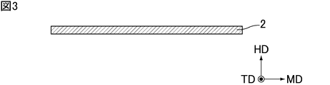
- FIG. 3 is a schematic cross-sectional view showing a step of producing a laminate in one example of the method for producing a resin film with a conductor layer of the present invention.
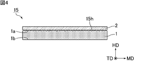
- FIG. 4 is a schematic cross-sectional view showing a step of producing a laminate in one example of the method for producing a resin film with a conductor layer of the present invention.
- FIG. 1 is a schematic cross-sectional view showing an example of the resin film with a conductor layer of the present invention.
- FIG. 2 is a schematic cross-sectional view showing a step of producing a laminate in one example of the method for producing a resin film with a conductor layer of the present invention.
- FIG. 3 is a
- FIG. 5 is an example of the resin film with a conductor layer of the present invention, and is a schematic cross-sectional view showing an example different from FIG.
- FIG. 6 is an example of the resin film with a conductor layer of the present invention, and is a schematic cross-sectional view showing an example different from FIGS. 1 and 5.
- FIG. 7 is a schematic cross-sectional view showing an example of the laminated substrate of the present invention.
- FIG. 8 is a schematic cross-sectional view showing a step of producing a resin film with a conductor layer in one example of the method for producing a laminated substrate of the present invention.
- FIG. 9 is a schematic cross-sectional view showing a step of producing a resin film with a conductor layer in one example of the method for producing a laminated substrate of the present invention.
- FIG. 10 is a schematic cross-sectional view showing a step of producing a resin film with a conductor layer in one example of the method for producing a laminated substrate of the present invention.
- FIG. 11 is a schematic cross-sectional view showing a step of forming via holes in one example of the method for manufacturing a laminated substrate of the present invention.
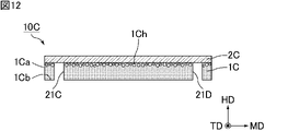
- FIG. 12 is a schematic cross-sectional view showing a step of forming via holes in one example of the method for manufacturing a laminated substrate of the present invention.
- FIG. 13 is a schematic cross-sectional view showing a step of filling a conductive paste in one example of the method for manufacturing a laminated substrate of the present invention.
- FIG. 14 is a schematic cross-sectional view showing a step of filling a conductive paste in one example of the method for manufacturing a laminated substrate of the present invention.
- FIG. 15 is a schematic cross-sectional view showing a step of forming interlayer connection conductors in one example of the method of manufacturing a laminated substrate of the present invention.
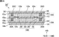
- FIG. 16 is an example of the laminated substrate of the present invention, and is a schematic cross-sectional view showing an example different from FIG.
- FIG. 17 is an example of the laminated substrate of the present invention, and is a schematic cross-sectional view showing an example different from FIGS.
- FIG. 18 is an example of the laminated substrate of the present invention, and is a schematic cross-sectional view showing an example different from FIGS.
- FIG. 19 is an example of the laminated substrate of the present invention, and is a schematic cross-sectional view showing an example different from FIGS.
- the resin film with a conductor layer of the present invention is described below. It should be noted that the present invention is not limited to the following configurations, and may be modified as appropriate without departing from the gist of the present invention.
- the present invention also includes a combination of the individual preferred configurations described below.
- the resin film with a conductor layer of the present invention includes a resin film containing a thermoplastic resin and having holes therein, and a conductor layer adjacent to at least one main surface side of the resin film in the lamination direction.
- the position of the end face on the conductor layer side is a first position
- the position separated from the first position in the lamination direction by a distance of 1/3 of the thickness of the resin film is a second position
- the holes are located at the first position.
- the second position is greater than the number of holes between the second position and the third position. It is characterized by being unevenly distributed in between.
- FIG. 1 is a schematic cross-sectional view showing an example of the resin film with a conductor layer of the present invention.
- a resin film 10 with a conductor layer shown in FIG. 1 has a resin film 1 and a conductor layer 2 in the stacking direction.
- a film is synonymous with a sheet, and the two are not distinguished by thickness.
- the lamination direction corresponds to the direction along the thickness direction of the resin film that constitutes the resin film with the conductor layer.
- the resin film 1 has a first main surface 1a and a second main surface 1b facing each other in the thickness direction HD.
- the thickness of the resin film 1 is preferably 10 ⁇ m or more and 250 ⁇ m or less.
- the first direction MD and the second direction TD are included in the in-plane direction perpendicular to the thickness direction HD. More specifically, the first direction MD is a direction orthogonal to the thickness direction HD, and the second direction TD is a direction orthogonal to the thickness direction HD and the first direction MD. That is, the thickness direction HD, the first direction MD, and the second direction TD are orthogonal to each other.
- the conductor layer 2 is adjacent to at least one main surface side of the resin film 1, here, the first main surface 1a side. More specifically, conductor layer 2 is provided on first main surface 1 a of resin film 1 .
- Examples of the constituent material of the conductor layer 2 include copper, silver, aluminum, stainless steel, nickel, gold, and alloys containing at least one of these metals.
- the conductor layer 2 is made of, for example, metal foil, and among metal foils, copper foil is preferable. In this case, a metal other than copper may be present on the surface of the copper foil.
- the resin film 1 contains a thermoplastic resin.
- thermoplastic resin contained in the resin film 1 examples include liquid crystal polymer (LCP), fluororesin, thermoplastic polyimide resin, polyether ether ketone resin (PEEK), polyphenylene sulfide resin (PPS), and cyclic polyolefin resin (COP). , polyphenylene ether resin (PPE), and the like.
- LCP liquid crystal polymer
- PEEK polyether ether ketone resin
- PPS polyphenylene sulfide resin
- COP cyclic polyolefin resin
- PPE polyphenylene ether resin
- the thermoplastic resin contained in the resin film 1 is preferably a liquid crystal polymer. That is, the resin film 1 is preferably a liquid crystal polymer film.
- the resin film 1 is preferably a liquid crystal polymer film.
- liquid crystal polymers have a low dielectric constant and low hygroscopicity. Therefore, in a laminated substrate manufactured using a liquid crystal polymer film, the dielectric properties in the high frequency range are likely to be improved. The effects of the liquid crystal polymer, such as the resistance to change in properties, are likely to be exhibited.
- the integrated value of the peak derived from the benzene ring in the 13 C-NMR spectrum of the resin film 1 decomposed with supercritical methanol is CA, naphthalene
- CB is the integrated value of the ring-derived peak
- CC is the integrated value of the carboxymethyl group-derived peak
- (CA+CB)/CC is preferably 1.25 or more and 1.65 or less.
- the coefficient of linear expansion in the thickness direction can be reduced by setting (CA+CB)/CC to 1.65 or less. Furthermore, in the liquid crystal polymer film, (CA + CB) / CC is 1.25 or more, so that the processing itself into a film state becomes easy, and further processing when manufacturing a laminated substrate using the liquid crystal polymer film easier to improve. Therefore, in the liquid crystal polymer film, when (CA + CB) / CC is 1.25 or more and 1.65 or less, the linear expansion coefficient in the thickness direction can be reduced, processability into a film state, and It is possible to improve workability when manufacturing a laminated substrate using a liquid crystal polymer film.
- (CA+CB)/CC is 1.25 or more and 1.65 or less when manufacturing a laminated substrate having an interlayer connection conductor using a liquid crystal polymer film, the linear expansion coefficient in the thickness direction of the liquid crystal polymer film is small. , stress is less likely to be applied from the liquid crystal polymer film to the interlayer connection conductor. Therefore, in a laminated substrate manufactured using a liquid crystal polymer film in which (CA+CB)/CC is 1.25 or more and 1.65 or less, cracks are less likely to occur in the interlayer connection conductors. Connection reliability is less likely to deteriorate.
- (CA+CB)/CC is preferably 1.35 or more and 1.65 or less.
- the liquid crystal polymer film is taken out.
- the liquid crystal polymer film is taken out by etching the conductor layer of the taken out liquid crystal polymer film with the conductor layer.
- the liquid crystal polymer film and methanol are placed in a high-temperature, high-pressure reactor. Then, the inside of the high-temperature and high-pressure reactor system is replaced with argon and then heated to obtain a solution in which the liquid crystal polymer film is dissolved. At this time, if the high-temperature and high-pressure reactor is a closed system, only by heating the inside of the system to, for example, 240° C. or higher, the methanol vaporizes and the inside of the system reaches the critical pressure of methanol. become supercritical.
- the solution is vacuum-dried to remove the solvent, thereby obtaining a powder of the decomposed product of the liquid crystal polymer film, which is in a state of being decomposed by supercritical methanol.
- a sample for NMR measurement is obtained by dissolving the powder of the decomposed product of the liquid crystal polymer film at a ratio of, for example, 0.02 g per 1 ml of heavy methanol.
- a 13 C-NMR spectrum is obtained by performing NMR measurement on the sample for NMR measurement. Then, from the 13 C-NMR spectrum, the integrated value of the peak derived from the benzene ring, the integrated value of the peak derived from the naphthalene ring, and the integrated value of the peak derived from the carboxymethyl group are obtained, CA, CB, and CC, respectively.
- the peak derived from the benzene ring is chemically The shift corresponds to the peak in the range of 113 ppm or more and 115 ppm or less (114 ⁇ 1 ppm).
- the peak derived from the naphthalene ring more specifically, the peak of methyl 6-hydroxy-2-naphthoate corresponds to the peak in the chemical shift range of 107 ppm or more and 109 ppm or less (108 ⁇ 1 ppm).
- a peak derived from a carboxymethyl group corresponds to a peak in a chemical shift range of 49 ppm or more and 51 ppm or less (50 ⁇ 1 ppm).
- CA, CB, and CC may be obtained as converted values when the integrated value of the peak derived from heavy methanol is 100, and then (CA+CB)/CC may be obtained.
- (CA+CB)/CC is controlled by, for example, using multiple types of wholly aromatic polyesters with different monomer primary structures as the liquid crystal polymer and adjusting the compounding ratio of these liquid crystal polymers during the production of the liquid crystal polymer film. .
- a liquid crystal polymer having a monomer primary structure in which (CA+CB)/CC is in the range of 1.25 or more and 1.65 or less may be used during the production of the liquid crystal polymer film.
- the surface of the inorganic filler is highly active, moisture is likely to be adsorbed on the surface of the inorganic filler. Therefore, in a laminated substrate manufactured using a liquid crystal polymer film containing an inorganic filler, the dielectric properties are likely to change due to moisture absorption. On the other hand, in order to lower the activity of the surface of the inorganic filler, the surface of the inorganic filler is sometimes treated with a coupling agent or the like. Adsorption of moisture cannot be sufficiently suppressed. In addition, the breaking elongation of the liquid crystal polymer film tends to decrease due to the inclusion of the inorganic filler.
- a liquid crystal polymer film having (CA+CB)/CC of 1.65 or less can have a small coefficient of linear expansion in the thickness direction. That is, a liquid crystal polymer film having (CA+CB)/CC of 1.65 or less does not need to contain an inorganic filler in order to reduce the coefficient of linear expansion in the thickness direction.
- the liquid crystal polymer film with a conductor layer having a liquid crystal polymer film in which (CA+CB)/CC is 1.65 or less and the laminated substrate having the liquid crystal polymer film with the conductor layer undergo a change in dielectric properties due to moisture absorption. become difficult. Furthermore, the elongation at break of the liquid crystal polymer film is less likely to decrease.
- a liquid crystal polymer film having (CA+CB)/CC of 1.65 or less can have a small coefficient of linear expansion in the thickness direction. That is, when producing a liquid crystal polymer film having (CA+CB)/CC of 1.65 or less, it is not necessary to irradiate a high dose of ionizing radiation in order to reduce the coefficient of linear expansion in the thickness direction. This reduces the manufacturing cost of the liquid crystal polymer film.
- CA is preferably 1.05 or more and 1.80 or less.
- the storage elastic modulus may increase.
- the coefficient of linear expansion in the thickness direction may increase.
- CB is preferably 1.20 or more and 1.70 or less.
- the coefficient of linear expansion in the thickness direction may increase.
- the storage elastic modulus may increase.
- CC is preferably 1.60 or more and 2.50 or less when the integrated value of the peak of is 100.
- the storage modulus may increase.
- the coefficient of linear expansion in the thickness direction may increase.
- a peak derived from heavy methanol corresponds to a peak in a range of chemical shifts of 47 ppm or more and 48 ppm or less (47.5 ⁇ 0.5 ppm).
- the resin film 1 is provided with holes 1h inside.
- the dielectric constant of the resin film 1 is reduced because the holes 1h are provided inside the resin film 1 .
- the laminated substrate manufactured using the resin film 10 with a conductor layer has improved dielectric properties in a high frequency region.
- the resin film 1 is a liquid crystal polymer film
- the dielectric properties of the laminated substrate in a high frequency region are significantly improved in combination with the effects of the liquid crystal polymer.
- the position of the first main surface 1a is the first position E1
- the thickness of the resin film 1 is increased in the lamination direction from the first position E1.
- a position separated by a distance of 1/3 is a second position E2
- a position separated by a distance of 1/3 of the thickness of the resin film 1 in the stacking direction from the second position E2 toward the opposite side of the first position E1 is called a second position.
- the number of holes 1h between the first position E1 and the second position E2 is larger than the number of holes between the second position E2 and the third position E3. It is unevenly distributed between the 1st position E1 and the 2nd position E2 so that it may increase.
- the holes 1h are unevenly distributed between the first position E1 and the second position E2 in the resin film 1 as described above, so that the holes 1h are located near the conductor layer 2. It means that it is unevenly distributed in In the laminated substrate manufactured using the resin film 10 with a conductor layer, when the conductor layer 2 is a signal line for transmitting signals, the holes 1h are unevenly distributed in the vicinity of the conductor layer 2, here, the signal line. As a result, the dielectric constant in the vicinity of the signal line is reduced, so that the transmission loss in the high frequency region is easily reduced, and as a result, the transmission characteristics in the high frequency region are easily improved.
- the second position in the resin film is a position separated from the interface between the resin film and the conductor layer included in the first position by a distance of 1/3 of the thickness of the resin film that overlaps the conductor layer in the lamination direction. , defined by a plane extending in an in-plane direction perpendicular to the stacking direction.
- the third position in the resin film is separated from the second position toward the side opposite to the first position in the lamination direction by a distance of 1/3 of the thickness of the resin film, which is the same as when the second position is determined. It is defined by a plane extending in an in-plane direction orthogonal to the stacking direction.
- the number of vacancies between the first position and the second position is determined as follows. First, for the resin film of the resin film with the conductor layer, or the resin film of the laminated substrate having the resin film with the conductor layer as described later, after confirming in advance the region where the holes exist from the thickness direction, the first A scanning electron microscope (SEM) captures an image of a cross section along the thickness direction when the region between the position and the second position is viewed from the in-plane direction. In this manner, cross-sectional images of the region between the first position and the second position on the resin film are photographed at 5 or more and 10 or less positions in the in-plane direction.
- SEM scanning electron microscope
- the size of one cross-sectional image is 75 ⁇ m long ⁇ 125 ⁇ m wide (for example, the size of the field of view when viewed at a magnification of 1000). Then, by performing image analysis on all cross-sectional images taken with image analysis software, the number of all pores in all cross-sectional images is counted, and one calculated from the total number of pores obtained The average value per cross-sectional image (one field of view) is defined as the number of holes between the first position and the second position.
- the number of holes between the second position and the third position is also determined in the same manner as the number of holes between the first position and the second position.
- the presence of voids cannot be confirmed in all cross-sectional images (cross-sectional images at 5 or more and 10 or less locations) taken for the area between the second position and the third position on the resin film. sets the number of vacancies between the second position and the third position to zero.
- the term "holes unevenly distributed between the first position and the second position” means that unlike the multilayer wiring board described in Patent Document 1 (see FIG. 1 of Patent Document 1), and the second position is extremely larger than the number of holes between the second position and the third position, preferably between the second position and the third position means that the number of vacancies between the positions is 1 ⁇ 5 or less of the number of vacancies between the first position and the second position.
- a fourth position is a position apart from the first position E1 in the stacking direction by a distance of 1/4 of the thickness of the resin film 1, and the fourth position is opposite to the first position E1.
- a fifth position is a position separated by a distance of 1/4 of the thickness of the resin film 1 in the stacking direction
- the holes 1h are located between the first position E1 and the fourth position. is unevenly distributed between the first position E1 and the fourth position so that the number of holes is greater than the number of holes between the fourth position E1 and the fifth position. In this case, the transmission characteristics in the high frequency region of the laminated substrate manufactured using the resin film 10 with a conductor layer are more likely to be improved.
- substantially no holes 1h exist between the second position E2 and the third position E3.
- the fact that there are substantially no holes between the second position and the third position means that the number of holes between the second position and the third position is 5 or less, preferably 3 or less. means a state.
- holes 1h may exist only between the first position E1 and the second position E2, as shown in FIG.
- the resin film 10 with a conductor layer it is possible to realize a resin film with a conductor layer that is capable of improving dielectric characteristics in a high frequency region with a configuration containing a thermoplastic resin.
- the hole diameter of the holes 1h existing between the first position E1 and the second position E2 is preferably 20 ⁇ m or less.
- the mechanical strength of the resin film 1 and, by extension, the mechanical strength of the resin film 10 with the conductor layer is less likely to decrease.
- the adhesiveness between the resin film 1 and the conductor layer 2 may deteriorate due to the holes 1h.
- the hole diameter of the holes 1h is 20 ⁇ m or less, even if the holes 1h are unevenly distributed near the conductor layer 2, the adhesion between the resin film 1 and the conductor layer 2 is less likely to decrease. .
- the hole diameter of the holes 1h is larger than 20 ⁇ m, the mechanical strength of the resin film 1 and, in turn, the mechanical strength of the resin film 10 with the conductor layer may decrease. Moreover, when the hole diameter of the holes 1h is larger than 20 ⁇ m, the adhesion between the resin film 1 and the conductor layer 2 may be deteriorated.
- the pore diameter of the pore 1h is preferably 5 ⁇ m or more.
- the hole diameter of the holes 1h is smaller than 5 ⁇ m, the number of the holes 1h for realizing the same porosity is too large compared to the case where the hole diameter of the holes 1h is 5 ⁇ m or more.
- the holes 1h may become the source of cracks, and as a result, the resin film with the conductor layer, or The mechanical strength of the laminated substrate having the resin film with the conductor layer may be lowered.
- the pore diameter of the pore existing between the first position and the second position is determined as follows. First, for the resin film of the resin film with the conductor layer, or the resin film of the laminated substrate having the resin film with the conductor layer as described later, after confirming in advance the region where the holes exist from the thickness direction, the first An image of a cross section along the thickness direction when the region between the position and the second position is viewed from the in-plane direction is photographed with a scanning electron microscope. In this manner, cross-sectional images of the region between the first position and the second position on the resin film are photographed at 5 or more and 10 or less positions in the in-plane direction.
- the size of one cross-sectional image is 75 ⁇ m long ⁇ 125 ⁇ m wide (for example, the size of the field of view when viewed at a magnification of 1000). Then, by performing image analysis on all cross-sectional images taken using image analysis software, the equivalent circle diameters of all pores in all cross-sectional images are measured, and the maximum of the obtained measured values is A value is defined as the pore diameter of the pore present between the first and second positions.
- the integrated value of the loss tangent in the temperature range from 40° C. to the melting point of the thermoplastic resin contained in the resin film is 29.7 or less. preferable.
- the integrated value of the loss tangent in the temperature range from 40°C to the melting point of the thermoplastic resin contained in the resin film is obtained as follows. First, a resin film is taken out by etching a conductor layer with respect to the resin film with a conductor layer. Alternatively, after taking out a resin film with a conductor layer from a laminated substrate having a resin film with a conductor layer as described later, the resin film is taken out by etching the conductor layer on the taken out resin film with a conductor layer. . Next, using a dynamic viscoelasticity measuring device, the temperature dependence of the loss tangent of the resin film is measured in a temperature range from at least 40 ° C.
- the graph showing the relationship between the loss tangent of and temperature is integrated in the temperature range from 40° C. to the melting point of the thermoplastic resin contained in the resin film to obtain the integrated value of the loss tangent.
- the melting point of the thermoplastic resin contained in the resin film is determined as follows. First, a differential scanning calorimeter is used to raise the temperature of the resin film to melt it completely. The resulting melt is then cooled and then heated again. Then, the temperature corresponding to the endothermic peak observed during this heating process is determined as the melting point of the thermoplastic resin contained in the resin film. If the endothermic peak is difficult to observe by the above method, the melting point of the thermoplastic resin contained in the resin film is determined by texture observation under crossed Nicols conditions with a polarizing microscope.
- the resin film 1 When the integrated value of the loss tangent of the resin film 1 under the above conditions is 29.7 or less, the resin film 1 has a small viscous component of the loss tangent of the viscoelastic properties and is less likely to soften even at high temperatures. The effect obtained when the resin film 1 has such properties will be described below while showing an example of the method of manufacturing the resin film 10 with the conductor layer shown in FIG.
- the method for producing a resin film with a conductor layer of the present invention has the resin film and the conductor layer in the stacking direction by providing the conductor layer so as to be adjacent to at least one main surface side of the resin film containing a thermoplastic resin. a step of forming a laminate; and a step of providing holes inside the resin film by heat-treating the laminate.
- the position of the end face of is the first position, the position separated from the first position by a distance of 1/3 of the thickness of the resin film in the lamination direction is the second position, and the second position is opposite to the first position
- a position separated by a distance of 1/3 of the thickness of the resin film in the lamination direction toward the third position is a third position
- the number of holes between the first position and the second position is the above
- the holes are unevenly distributed between the first position and the second position so as to be larger than the number of holes between the second position and the third position.
- ⁇ Step of producing a laminate> 2 3, and 4 are cross-sectional schematic diagrams showing the steps of producing a laminate in one example of the method for producing a resin film with a conductor layer of the present invention.
- a resin film 1 containing a thermoplastic resin is prepared.
- the first main surface 1a of the resin film 1 is not a completely flat surface but a rough surface with irregularities.
- the resin film 1 for example, a liquid crystal polymer film, is produced by a known method such as that described in JP-A-2-3430 using a resin material containing a liquid crystal polymer.
- a film forming method for the resin film 1 for example, a liquid crystal polymer film, a T-die film forming stretching method, a laminate stretching method, an inflation method, and the like are industrially advantageous.
- a conductor layer 2 is prepared.
- the resin film 1 and the conductor layer 2 are laminated by providing the conductor layer 2 so as to be adjacent to at least one main surface side of the resin film 1, here, the first main surface 1a side.
- a laminate 15 having an orientation is produced.
- the conductor layer 2 is pressure-bonded to the first main surface 1a of the resin film 1 .
- the first main surface 1a of the resin film 1 is a rough surface, a space 15h is provided between the resin film 1 and the conductor layer 2 in the in-plane direction.
- the main surface of the resin film 1 on which the conductor layer 2 is provided here, the arithmetic mean height Sa of the first main surface 1a is preferably 240 nm or more.
- the arithmetic mean height Sa of the main surface of the resin film 1 on the side where the conductor layer 2 is provided, here, the first main surface 1a is 240 nm or more, a space is formed between the resin film 1 and the conductor layer 2. 15h is more likely to be provided in a wider range. As a result, in the step of forming holes, which will be described later, the holes originating from the space 15h are likely to be formed in a wider range near the conductor layer 2 in the resin film 1 . Therefore, in the resin film with a conductor layer to be obtained later, the number of holes in the vicinity of the conductor layer 2 in the resin film 1 tends to increase.
- the main surface of the resin film 1 on which the conductor layer 2 is provided here, the arithmetic mean height Sa of the first main surface 1a is preferably 350 nm or less.
- the arithmetic mean height Sa of the main surface of the resin film on which the conductor layer is provided is determined as follows. First, of the main surface of the resin film, an image for nine fields of view is photographed at a magnification of 20 using a non-contact laser microscope with respect to the portion where the conductor layer is to be provided. Then, by performing image analysis on all the captured images with image analysis software, the arithmetic mean height Sa of the main surface of the resin film in each image is measured, and the maximum of the obtained measured values The value is defined as the arithmetic mean height Sa of the main surface of the resin film on the side where the conductor layer is provided.
- Pores are provided inside the resin film 1 by heat-treating the laminate 15 . At this time, when the laminated body 15 is heat-treated, the resin film 1 flows and the space 15h is taken into the inside of the resin film 1 . As a result, pores originating from the space 15h are provided inside the resin film 1 . More specifically, as shown in FIG.
- the position of the first main surface 1a is the first position E1
- the resin A position separated by a distance of 1/3 of the thickness of the film 1 is a second position E2
- a distance of 1/3 of the thickness of the resin film 1 is provided in the stacking direction from the second position E2 toward the opposite side of the first position E1.
- the distant position is the third position E3
- the number of holes between the first position E1 and the second position E2 is greater than the number of holes between the second position E2 and the third position E3.
- the holes 1h are provided so as to be unevenly distributed between the first position E1 and the second position E2.
- the conductor layer-attached resin film 10 shown in FIG. 1 is manufactured.
- the resin The film 1 has a low viscous component of the loss tangent of viscoelastic properties, and is hard to soften even at high temperatures.
- the resin film 1 has such properties, the resin film 1 is less likely to be softened, so that the uneven shape provided on the first main surface 1a of the resin film 1 can be easily maintained.
- the gas contained in the space 15h originating from the unevenness provided on the first main surface 1a of the resin film 1 is released into the resin film 1. It becomes difficult to escape to the outside. As a result, the gas contained in the space 15h is more likely to be taken into the resin film 1. Therefore, as shown in FIG. 1h is easily provided.
- the resin film with a conductor layer of the present invention may have a planar shape in which the conductor layer spreads all over like the resin film with a conductor layer 10 shown in FIG. It may be a pattern shape.
- FIG. 5 is an example of the resin film with a conductor layer of the present invention, and is a schematic cross-sectional view showing an example different from FIG.
- a resin film 10' with a conductor layer shown in FIG. 5 has a resin film 1 and a conductor layer 2' in the stacking direction.
- the conductor layer 2' is adjacent to the resin film 1 on the side of the first main surface 1a. More specifically, the conductor layer 2 ′ is provided on part of the first main surface 1 a of the resin film 1 .
- the conductor layer 2' is formed, for example, by pressing a conductor layer onto the first main surface 1a of the resin film 1 and then etching the conductor layer into a pattern shape.
- the conductor layer 2 ′ may be formed by pressing a pre-patterned conductor layer onto the first main surface 1 a of the resin film 1 .
- the end surface of the resin film 1 on the side of the conductor layer 2' here, the position of the first main surface 1a is set to the first position E1, and the resin film 1 is moved in the lamination direction from the first position E1.
- a position separated by a distance of 1/3 of the thickness is a second position E2, and a position separated by a distance of 1/3 of the thickness of the resin film 1 in the stacking direction from the second position E2 toward the opposite side of the first position E1.
- the third position E3 is the third position E3
- the number of holes 1h between the first position E1 and the second position E2 is the number of holes between the second position E2 and the third position E3 It is unevenly distributed between the first position E1 and the second position E2 so as to be greater than that.
- the holes 1h are formed in the vicinity of the region where the conductor layer 2' is provided on the first main surface 1a of the resin film 1, and in addition, the conductor layer 2' is not provided. It also exists in the vicinity of the area. That is, in the conductor layer-attached resin film 10', the holes 1h do not overlap the conductor layer 2' when viewed in the thickness direction HD, in addition to the regions overlapping the conductor layer 2' when viewed in the thickness direction HD. also exist in the area.
- the resin film with a conductor layer of the present invention may have a conductor layer adjacent only to one main surface side of the resin film like the resin film 10 with a conductor layer shown in FIG.
- the resin film may have another conductor layer adjacent to the other principal surface side.
- FIG. 6 is an example of the resin film with a conductor layer of the present invention, which is a schematic cross-sectional view showing an example different from FIGS.
- a resin film 10'' with a conductor layer shown in FIG. 6 has a resin film 1'', a conductor layer 2, and a conductor layer 2'' in the stacking direction.
- the resin film 1'' has a first main surface 1a'' and a second main surface 1b'' facing in the thickness direction HD.
- the conductor layer 2 is adjacent to the first main surface 1a'' side of the resin film 1''. More specifically, the conductor layer 2 is provided on the first major surface 1a'' of the resin film 1''.
- the conductor layer 2'' is adjacent to the second main surface 1b'' side of the resin film 1''. More specifically, the conductor layer 2'' is provided on the second main surface 1b'' of the resin film 1''.
- the resin film 1'' contains a thermoplastic resin.
- the resin film 1'' has holes 1h inside.
- the position of the first main surface 1a'' is set to the first position E1, and from the first position E1 in the lamination direction
- a position separated by a distance of 1/3 of the thickness of the resin film 1'' is the second position E2, and from the second position E2 toward the side opposite to the first position E1, the thickness of the resin film 1'' is 1'' in the stacking direction.
- /3 is the third position E3
- the number of holes between the first position E1 and the second position E2 is are unevenly distributed between the first position E1 and the second position E2 so that the number of holes is greater than the number of holes between the positions E1 and E2. That is, in the conductor layer-attached resin film 10 ′′, the holes 1 h are unevenly distributed near the conductor layer 2 .
- holes 1h'' are provided inside the resin film 1'' in addition to the holes 1h.
- the end surface of the resin film 1'' on the side of the conductor layer 2'', here, the position of the second main surface 1b'' is designated as the first position E1'', and the first position E1.
- '' in the stacking direction to a second position E2'', and from the second position E2'' toward the opposite side of the first position E1''.
- a third position E3'' is a position separated by a distance of 1/3 of the thickness of the resin film 1'' in the stacking direction
- the holes 1h'' are located at a first position E1'' and a second position E2'. ' is greater than the number of vacancies between the second position E2'' and the third position E3''. '' and are unevenly distributed. That is, in the resin film 10'' with a conductor layer, the holes 1h'' are unevenly distributed in the vicinity of the conductor layer 2''.
- the laminated substrate of the present invention is characterized by comprising the resin film with a conductor layer of the present invention.
- FIG. 7 is a schematic cross-sectional view showing an example of the laminated substrate of the present invention.
- a laminated substrate 50 shown in FIG. 7 has a conductor layer-attached resin film 10A, a conductor layer-attached resin film 10B, and a conductor layer-attached resin film 10C in this order in the stacking direction. That is, in the laminated substrate 50, the resin film 10A with the conductor layer, the resin film 10B with the conductor layer, and the resin film 10C with the conductor layer are laminated in order in the lamination direction.
- the resin film 10A with a conductor layer has a resin film 1A and a conductor layer 2A.
- the resin film 1A has a first main surface 1Aa and a second main surface 1Ab facing each other in the thickness direction HD.
- the conductor layer 2A is adjacent to the first main surface 1Aa side of the resin film 1A.
- the conductor layer 2A is also adjacent to the second main surface 1Bb side of the resin film 1B, which will be described later.
- the resin film 1A contains a thermoplastic resin.
- the resin film 1A is internally provided with holes 1Ah.
- the position of the first main surface 1Aa is the first position EA1
- the thickness of the resin film 1A is increased in the lamination direction from the first position EA1.
- a position separated by a distance of 1 ⁇ 3 is a second position EA2, and a position separated by a distance of 1 ⁇ 3 of the thickness of the resin film 1A in the stacking direction from the second position EA2 toward the side opposite to the first position EA1 is designated as a second position.
- the number of holes 1Ah between the first position EA1 and the second position EA2 is greater than the number of holes between the second position EA2 and the third position EA3. It is unevenly distributed between the first position EA1 and the second position EA2 so as to increase. That is, in the resin film 10A with a conductor layer, the holes 1Ah are unevenly distributed near the conductor layer 2A.
- the resin film 10B with a conductor layer has a resin film 1B, a conductor layer 2B, a conductor layer 2B', and a conductor layer 2B''.
- the resin film 1B has a first main surface 1Ba and a second main surface 1Bb facing each other in the thickness direction HD.
- the conductor layer 2B, the conductor layer 2B', and the conductor layer 2B'' are adjacent to the first main surface 1Ba side of the resin film 1B. Moreover, the conductor layer 2B, the conductor layer 2B', and the conductor layer 2B'' are also adjacent to the second main surface 1Cb side of the resin film 1C, which will be described later.
- the resin film 1B contains a thermoplastic resin.
- the resin film 1B is internally provided with holes 1Bh.
- the position of the first main surface 1Ba is set to the first position EB1
- the A second position EB2 is located at a distance of 1 ⁇ 3 of the thickness of the resin film 1B in the stacking direction from the first position EB1
- the resin film 1B is placed in the stacking direction from the second position EB2 toward the side opposite to the first position EB1.
- the number of holes between the first position EB1 and the second position EB2 is the number of holes 1Bh between the second position EB2 and the They are unevenly distributed between the first position EB1 and the second position EB2 so that the number of holes is greater than the number between the three positions EB3. That is, in the conductor layer-attached resin film 10B, the holes 1Bh are unevenly distributed in the vicinity of the conductor layer 2B, the conductor layer 2B', and the conductor layer 2B''.
- the holes 1Bh are arranged in the conductor layer 2B, the conductor layer 2B′, and the conductor layer 2B. Then, from the main surface (here, the lower surface) in the stacking direction of the conductor layer 2B'', the conductor layers 2B, 2B', and side surfaces (here, the left side and right side).
- a resin film 10C with a conductor layer has a resin film 1C and a conductor layer 2C.
- the resin film 1C has a first main surface 1Ca and a second main surface 1Cb facing each other in the thickness direction HD.
- the conductor layer 2C is adjacent to the first main surface 1Ca side of the resin film 1C.
- the resin film 1C contains a thermoplastic resin.
- the resin film 1C is internally provided with holes 1Ch.
- the position of the first main surface 1Ca is the first position EC1
- the thickness of the resin film 1C is increased in the lamination direction from the first position EC1.
- a position separated by a distance of 1/3 is a second position EC2
- a position separated by a distance of 1/3 of the thickness of the resin film 1C in the stacking direction from the second position EC2 toward the opposite side of the first position EC1 is called a second position.
- the number of holes 1Ch between the first position EC1 and the second position EC2 is greater than the number of holes between the second position EC2 and the third position EC3. As many as possible, they are unevenly distributed between the first position EC1 and the second position EC2. That is, in the conductor layer-attached resin film 10C, the holes 1Ch are unevenly distributed in the vicinity of the conductor layer 2C.
- the conductor layer 2B is preferably provided across the interface between the resin film 1B and the resin film 1C, as shown in FIG. As a result, the interface between the conductor layer 2B and the resin film 1B and the interface between the conductor layer 2B and the resin film 1C are displaced in the stacking direction from the interface between the resin film 1B and the resin film 1C. Peeling at the interface with the film 1B and peeling at the interface between the conductor layer 2B and the resin film 1C are suppressed.
- the conductor layer 2B' and the conductor layer 2B'' are also provided across the interface between the resin film 1B and the resin film 1C, like the conductor layer 2B.
- the dielectric characteristics in the high frequency region are improved. Furthermore, when the resin film 1A, the resin film 1B, and the resin film 1C are liquid crystal polymer films, the dielectric properties of the laminated substrate 50 in the high frequency region are significantly improved in combination with the effects of the liquid crystal polymer.
- the pores are unevenly distributed near the conductor layer.
- the conductor layer is a signal line for transmitting a signal
- the laminated substrate 50 manufactured using the resin film 10A with the conductor layer, the resin film 10B with the conductor layer, and the resin film 10C with the conductor layer does not have the conductor layer
- the dielectric constant in the vicinity of the signal line is reduced, the transmission loss in the high frequency region is easily reduced, and as a result, the transmission characteristics in the high frequency region are improved. easier to improve.
- the resin films with the conductor layer have the first position, the second position, and the third position as described above.
- the position it is preferable that the holes are unevenly distributed between the first position and the second position, but in some resin films with a conductor layer, the holes are located at the first position and the second position It may be unevenly distributed between That is, as long as the laminated substrate 50 has at least one resin film with a conductor layer in which the holes are unevenly distributed between the first position and the second position, the holes are located at the first position and the second position.
- Preferred features of the conductor layer-attached resin film 10A, the conductor layer-attached resin film 10B, and the conductor layer-attached resin film 10C are the same as the preferable features of the conductor layer-attached resin film 10 described above. That is, the preferred features of the resin film 1A, the resin film 1B, and the resin film 1C are the same as the preferred features of the resin film 1 described above.
- the thicknesses of the resin film 1A, the resin film 1B, and the resin film 1C may be the same as each other, may be different from each other, or may be partially different as shown in FIG.
- the constituent material of the conductor layer 2A, the conductor layer 2B, the conductor layer 2B', the conductor layer 2B'', and the conductor layer 2C similar to the constituent material of the conductor layer 2, for example, copper, silver, aluminum, stainless steel, Examples include nickel, gold, and alloys containing at least one of these metals.
- the conductor layer 2A, the conductor layer 2B, the conductor layer 2B', the conductor layer 2B'', and the conductor layer 2C are made of metal foil, for example, like the conductor layer 2, and among the metal foils, copper foil may be used. preferable. In this case, a metal other than copper may be present on the surface of the copper foil.
- the constituent materials of the conductor layer 2A, the conductor layer 2B, the conductor layer 2B', the conductor layer 2B'', and the conductor layer 2C are preferably the same, but may be different from each other, or partially different. may be
- the thicknesses of the conductor layer 2A, the conductor layer 2B, the conductor layer 2B', the conductor layer 2B'', and the conductor layer 2C may be the same as shown in FIG. 7, or may be different. , may be different in part.
- the laminated substrate 50 further has an interlayer connection conductor that penetrates the resin film in the lamination direction but does not penetrate the conductor layer in the lamination direction and is connected to the conductor layer. preferably.
- the laminated substrate 50 shown in FIG. 7 further has an interlayer connection conductor 20A, an interlayer connection conductor 20B, an interlayer connection conductor 20C, and an interlayer connection conductor 20D.
- the interlayer connection conductor 20A is provided so as to penetrate the resin film 1B in the stacking direction, but not penetrate the conductor layer 2B' in the stacking direction, and be connected to the conductor layer 2B'. More specifically, the interlayer connection conductor 20A penetrates the resin film 1B in the stacking direction and is connected to the conductor layer 2B' on the first main surface 1Ba side of the resin film 1B. Further, the interlayer connection conductor 20A is connected to the conductor layer 2A on the second main surface 1Bb side of the resin film 1B. That is, the conductor layers 2A and 2B' are electrically connected via the interlayer connection conductor 20A.
- the interlayer connection conductor 20B penetrates the resin film 1B in the stacking direction but does not penetrate the conductor layer 2B'' in the stacking direction at a position separated from the interlayer connection conductor 20A, and is connected to the conductor layer 2B''.
- the interlayer connection conductor 20B penetrates the resin film 1B in the stacking direction at a position spaced apart from the interlayer connection conductor 20A, and is connected to the conductor layer 2B'' on the first main surface 1Ba side of the resin film 1B. It is connected.
- the interlayer connection conductor 20B is connected to the conductor layer 2A on the second main surface 1Bb side of the resin film 1B at a position separated from the interlayer connection conductor 20A. That is, the conductor layer 2A and the conductor layer 2B'' are electrically connected via the interlayer connection conductor 20B.
- the interlayer connection conductor 20C penetrates the resin film 1C in the stacking direction, but does not penetrate the conductor layer 2C in the stacking direction, and is provided so as to be connected to the conductor layer 2C. More specifically, the interlayer connection conductor 20C penetrates the resin film 1C in the stacking direction and is connected to the conductor layer 2C on the first main surface 1Ca side of the resin film 1C. Also, the interlayer connection conductor 20C is connected to the conductor layer 2B' on the second main surface 1Cb side of the resin film 1C. That is, the conductor layer 2B' and the conductor layer 2C are electrically connected via the interlayer connection conductor 20C.
- the interlayer connection conductor 20D is provided at a position separated from the interlayer connection conductor 20C so as to be connected to the conductor layer 2C without penetrating the resin film 1C in the lamination direction but not through the conductor layer 2C in the lamination direction.
- the interlayer connection conductor 20D is connected to the conductor layer 2C on the first main surface 1Ca side of the resin film 1C while penetrating the resin film 1C in the stacking direction at a position separated from the interlayer connection conductor 20C.
- the interlayer connection conductor 20D is connected to the conductor layer 2B'' on the second main surface 1Cb side of the resin film 1C at a position separated from the interlayer connection conductor 20C. That is, the conductor layer 2B'' and the conductor layer 2C are electrically connected via the interlayer connection conductor 20D.
- the conductor layers 2A and 2C are electrically connected via the interlayer connection conductors 20A, the conductor layers 2B', and the interlayer connection conductors 20C.
- the conductor layers 2A and 2C are also electrically connected via the interlayer connection conductors 20B, the conductor layers 2B'', and the interlayer connection conductors 20D.
- the interlayer connection conductor 20A is provided on the inner wall of the via hole provided to reach the conductor layer 2B' without penetrating the conductor layer 2B' in the thickness direction HD, but not through the resin film 1B in the thickness direction HD. It is formed by performing a plating process or performing a heat treatment after filling the conductive paste.
- the interlayer connection conductor 20B, the interlayer connection conductor 20C, and the interlayer connection conductor 20D are also formed in the same manner as the interlayer connection conductor 20A, except that the formation positions are different.
- interlayer connection conductor 20A, the interlayer connection conductor 20B, the interlayer connection conductor 20C, and the interlayer connection conductor 20D are formed by plating
- metals that constitute the interlayer connection conductors include copper, tin, and silver. Among them, copper is preferred.
- each interlayer connection conductor includes, for example, copper and tin. , silver and the like.
- each interlayer connection conductor preferably contains copper, more preferably copper and tin.
- the interlayer connection conductor 20A contains copper and tin and the conductor layer 2B' is made of copper foil, the interlayer connection conductor 20A and the conductor layer 2B' undergo an alloying reaction at low temperature, so that they are easily conductive.
- the resin contained in each interlayer connection conductor is epoxy resin, phenol resin, At least one thermosetting resin selected from the group consisting of polyimide resin, silicone resin or modified resin thereof, and acrylic resin, or polyamide resin, polystyrene resin, polymethacrylic resin, polycarbonate resin, and cellulose resin It preferably contains at least one thermoplastic resin selected from the group consisting of
- the laminated board 50 is used, for example, as an electronic circuit board.
- the conductor layer 2B may be a signal line for transmitting signals. That is, the laminated substrate 50 may have the conductor layer 2B as a signal line for transmitting signals. In this case, the laminated substrate 50 constitutes a transmission line.
- the conductor layer 2B when the conductor layer 2B is a signal line for transmitting signals, as shown in FIG. preferably extends from the main surface (here, the bottom surface) in the stacking direction of the conductor layer 2B to the side surfaces (here, the left side and the right side) in the in-plane direction of the conductor layer 2B.
- the conductor layer 2B transmits a signal as a signal line
- the electric field tends to concentrate at the corners of the conductor layer 2B.
- the holes 1Bh extend from the main surface of the conductor layer 2B in the stacking direction to the side surfaces of the conductor layer 2B in the in-plane direction, the holes 1Bh cross the corners of the conductor layer 2B. Since it exists so as to cover it, the transmission loss in the high-frequency region is likely to be reduced, and as a result, the transmission characteristics in the high-frequency region are likely to be improved.
- the laminated substrate 50 may have the conductor layer 2B as a signal line for transmitting signals, and the conductor layers 2A and 2C as ground electrodes. In this case, the laminated substrate 50 constitutes a stripline type transmission line.
- the conductor layer 2B may be a signal line for transmitting high frequency signals.
- the holes 1Bh are unevenly distributed in the vicinity of the conductor layer 2B, that is, in the vicinity of the signal line, so the dielectric constant in the vicinity of the signal line is reduced. Therefore, when the laminated substrate 50 constitutes a transmission line, the transmission loss in the high frequency range is likely to be reduced, and as a result, the transmission characteristics in the high frequency range are likely to be improved.
- the laminated substrate 50 is manufactured, for example, by the following method.
- Step of producing a resin film with a conductor layer> 8 9, and 10 are cross-sectional schematic diagrams showing steps of producing a resin film with a conductor layer in one example of the method for producing a laminated substrate of the present invention.
- a resin film 10A with a conductor layer is produced in which a conductor layer 2A is provided so as to be adjacent to the first main surface 1Aa side of the resin film 1A.
- the resin film 10A with a conductor layer is produced, for example, in the same manner as the resin film 10 with a conductor layer. Thereby, in the resin film 10A with a conductor layer, the holes 1Ah are provided so as to be unevenly distributed in the vicinity of the conductor layer 2A.
- a resin film 10B with a conductor layer provided with a conductor layer 2B, a conductor layer 2B′, and a conductor layer 2B′′ adjacent to the first main surface 1Ba of the resin film 1B is prepared. make.
- the resin film 10B with a conductor layer is produced, for example, in the same manner as the resin film 10 with a conductor layer. Accordingly, in the resin film 10B with a conductor layer, the holes 1Bh are provided so as to be unevenly distributed in the vicinity of the conductor layer 2B, the conductor layer 2B', and the conductor layer 2B''.
- the conductor layer is etched to form the conductor layer 2B, the conductor layer 2B', and the The conductor layer 2B'' is patterned.
- the conductor layer 2B, the conductor layer 2B', and the conductor layer 2B'' are prepared in advance, and each conductor layer is pressure-bonded to the first main surface 1Ba of the resin film 1B.
- a resin film 10C with a conductor layer is produced in which a conductor layer 2C is provided so as to be adjacent to the first main surface 1Ca side of the resin film 1C.
- the resin film 10C with a conductor layer is produced, for example, in the same manner as the resin film 10 with a conductor layer. Thereby, in the resin film 10C with a conductor layer, the holes 1Ch are provided so as to be unevenly distributed in the vicinity of the conductor layer 2C.
- ⁇ Step of Forming Via Hole> 11 and 12 are schematic cross-sectional views showing steps of forming via holes in an example of the method for manufacturing a laminated substrate of the present invention.
- the resin film 1B is penetrated in the thickness direction HD, but the conductor layer 2B' is not penetrated in the thickness direction HD to reach the conductor layer 2B'.
- a via hole 21A is formed. As a result, a portion of the conductor layer 2B' is exposed from the via hole 21A.
- the resin film 1B is penetrated in the thickness direction HD, but the conductor layer 2B'' is not penetrated in the thickness direction HD.
- a via hole 21B is formed to reach the conductor layer 2B''. As a result, a portion of the conductor layer 2B'' is exposed from the via hole 21B.
- the via holes 21A and 21B are formed in the conductor layer-attached resin film 10B.
- the via hole 21A and the via hole 21B may be formed at the same timing or may be formed at different timings.
- a via hole 21C is formed in a resin film 10C with a conductor layer so as to penetrate the resin film 1C in the thickness direction HD but not penetrate the conductor layer 2C in the thickness direction HD to reach the conductor layer 2C. to form As a result, a portion of the conductor layer 2C is exposed from the via hole 21C.
- the resin film 10C with the conductor layer is penetrated in the thickness direction HD, but the conductor is not penetrated through the conductor layer 2C in the thickness direction HD.
- a via hole 21D is formed to reach the layer 2C. As a result, a portion of the conductor layer 2C is exposed from the via hole 21D.
- the via holes 21C and 21D are formed in the resin film 10C with the conductor layer. At this time, the via hole 21C and the via hole 21D may be formed at the same timing or may be formed at different timings.
- the via hole 21A, the via hole 21B, the via hole 21C, and the via hole 21D it is preferable to irradiate the resin film with the conductor layer with a laser beam from the resin film side.
- Step of filling conductive paste> 13 and 14 are cross-sectional schematic diagrams showing a step of filling a conductive paste in one example of the method for manufacturing a laminated substrate of the present invention.
- the conductive paste 22A is filled into the via holes 21A of the resin film 10B with the conductor layer.
- the conductive paste 22B is filled into the via holes 21B of the resin film 10B with the conductor layer.
- the conductive paste 22A and the conductive paste 22B may be filled at the same timing or at different timings.
- the conductive paste 22C is filled into the via holes 21C of the resin film 10C with the conductor layer.
- the conductive paste 22D is filled into the via holes 21D of the resin film 10C with the conductive layer.
- the conductive paste 22C and the conductive paste 22D may be filled at the same timing or may be filled at different timings.
- Examples of methods for filling the conductive paste 22A, the conductive paste 22B, the conductive paste 22C, and the conductive paste 22D include a screen printing method and a vacuum filling method.
- the conductive paste 22A, the conductive paste 22B, the conductive paste 22C, and the conductive paste 22D each contain metal and resin, for example.
- each conductive paste preferably contains copper, and more preferably contains copper and tin.
- the resin contained in each of the conductive pastes of the conductive paste 22A, the conductive paste 22B, the conductive paste 22C, and the conductive paste 22D includes epoxy resin, phenol resin, polyimide resin, silicon resin or modified resin thereof, and , At least one thermosetting resin selected from the group consisting of acrylic resins, or at least one selected from the group consisting of polyamide resins, polystyrene resins, polymethacrylic resins, polycarbonate resins, and cellulose resins It preferably contains a thermoplastic resin.
- Each conductive paste of the conductive paste 22A, the conductive paste 22B, the conductive paste 22C, and the conductive paste 22D may further contain a vehicle, a solvent, a thixotropic agent, an activator, and the like.
- Examples of the vehicle include rosin-based resins composed of rosin and its derivatives such as modified rosin, synthetic resins composed of rosin and its derivatives such as modified rosin, and mixtures of these resins. .
- rosin-based resins composed of rosin and derivatives thereof such as modified rosin include gum rosin, tall rosin, wood rosin, polymerized rosin, hydrogenated rosin, formylated rosin, rosin ester, rosin-modified maleic acid resin, and rosin-modified phenol.
- examples include resins, rosin-modified alkyd resins, and other various rosin derivatives.
- Examples of synthetic resins composed of rosin and derivatives such as modified rosin obtained by modifying rosin include polyester resins, polyamide resins, phenoxy resins, and terpene resins.
- solvents include alcohols, ketones, esters, ethers, aromatics, and hydrocarbons. Specific examples thereof include benzyl alcohol, ethanol, isopropyl alcohol, butanol, diethylene glycol, ethylene glycol, glycerin, ethyl cellosolve, butyl cellosolve, ethyl acetate, butyl acetate, butyl benzoate, diethyl adipate, dodecane, tetradecene, ⁇ -terpineol.
- terpineol 2-methyl-2,4-pentanediol, 2-ethylhexanediol, toluene, xylene, propylene glycol monophenyl ether, diethylene glycol monohexyl ether, ethylene glycol monobutyl ether, diethylene glycol monobutyl ether, diethylene glycol monoethyl ether, diisobutyl adipate, hexylene glycol, cyclohexanedimethanol, 2-terpinyloxyethanol, 2-dihydroterpinyloxyethanol, mixtures thereof, and the like.
- terpineol ethylene glycol monobutyl ether, diethylene glycol monobutyl ether, or diethylene glycol monoethyl ether is preferable.
- thixotropic agents include hydrogenated castor oil, carnauba wax, amides, hydroxy fatty acids, dibenzylidene sorbitol, bis(p-methylbenzylidene) sorbitols, beeswax, stearic acid amide, hydroxystearic acid ethylene bisamide, and the like.
- thixotropic agents may optionally contain fatty acids such as caprylic acid, lauric acid, myristic acid, palmitic acid, stearic acid and behenic acid, hydroxy fatty acids such as 1,2-hydroxystearic acid, and antioxidants. , surfactants, amines and the like may be added.
- activators include amine hydrohalides, organic halogen compounds, organic acids, organic amines, and polyhydric alcohols.
- Amine hydrohalides include, for example, diphenylguanidine hydrobromide, diphenylguanidine hydrochloride, cyclohexylamine hydrobromide, ethylamine hydrochloride, ethylamine hydrobromide, diethylaniline hydrobromide salts, diethylaniline hydrochloride, triethanolamine hydrobromide, monoethanolamine hydrobromide and the like.
- organic halogen compounds include paraffin chloride, tetrabromoethane, dibromopropanol, 2,3-dibromo-1,4-butanediol, 2,3-dibromo-2-butene-1,4-diol, tris(2 , 3-dibromopropyl) isocyanurate and the like.
- organic acids examples include malonic acid, fumaric acid, glycolic acid, citric acid, malic acid, succinic acid, phenylsuccinic acid, maleic acid, salicylic acid, anthranilic acid, glutaric acid, suberic acid, adipic acid, sebacic acid, stearic acid, abietic acid, benzoic acid, trimellitic acid, pyromellitic acid, dodecanoic acid and the like.
- organic amines examples include monoethanolamine, diethanolamine, triethanolamine, tributylamine, aniline, and diethylaniline.
- polyhydric alcohols examples include erythritol, pyrogallol, and ribitol.
- FIG. 15 is a schematic cross-sectional view showing a step of forming interlayer connection conductors in one example of the method for manufacturing a laminated substrate of the present invention.
- a resin film 10A with a conductor layer, a resin film 10B with a conductor layer filled with a conductive paste 22A and a conductive paste 22B, and a conductor filled with a conductive paste 22C and a conductive paste 22D 10 C of resin films with a layer are laminated
- the surface (upper surface) of the resin film 10A with the conductor layer on the side of the conductor layer 2A and the surface (lower surface) of the resin film 10B with the conductor layer on the side of the resin film 1B are in contact with each other, and the resin film 10B with the conductor layer is in contact with each other.
- the obtained laminate is subjected to hot pressing by applying pressure in the lamination direction while heating. Thereby, the resin film 10A with the conductor layer and the resin film 10B with the conductor layer are crimped, and the resin film 10B with the conductor layer and the resin film 10C with the conductor layer are crimped.
- the resin film 10B with the conductor layer and the resin film 10C with the conductor layer are pressure-bonded, since the resin film 1B contains the thermoplastic resin, the conductor layer 2B, the conductor layer 2B', and the conductor layer 2B'' is pushed into the resin film 1B.
- the vacancies 1Bh move together with the conductor layers 2B, 2B', and 2B'', so that the vacancies 1Bh move along the conductor layers 2B, 2B', and 2B''.
- the conductor layer 2B, the conductor layer 2B', and the conductor layer 2B'' are present so as to wrap around the side surfaces in the in-plane direction.
- the holes 1Bh extend from the main surface of the conductor layer 2B, the conductor layer 2B', and the conductor layer 2B'' in the stacking direction of the conductor layer 2B, the conductor layer 2B', and the conductor layer 2B''.
- the structure that exists so as to wrap around the side surface in the in-plane direction is a collective lamination method using a resin film 10B with a conductor layer in which holes 1Bh are provided inside the resin film 1B containing a thermoplastic resin, more specifically, , the conductor layer-attached resin film 10B and the conductor layer-attached resin film 10C are collectively laminated.
- the conductive paste 22A, the conductive paste 22B, the conductive paste 22C, and the conductive paste 22D are solidified during the hot press processing, thereby forming the interlayer connection conductor 20A, the interlayer connection conductor 20B, and the interlayer connection conductor 20C, respectively. , and an interlayer connection conductor 20D.
- interlayer connection conductors 20A, 20B, 20C, and 20D are formed in via holes 21A, 21B, 21C, and 21D, respectively.
- the interlayer connection conductor 20A When forming the interlayer connection conductor 20A, the interlayer connection conductor 20B, the interlayer connection conductor 20C, and the interlayer connection conductor 20D, instead of filling the via hole with a conductive paste, a metal such as copper, tin, or silver is used.
- a metal such as copper, tin, or silver is used.
- the inner wall of the via hole may be plated.
- the laminated substrate 50 shown in FIG. 7 is manufactured.
- the laminated substrate of the present invention may further include side conductors on the side surfaces along the lamination direction.
- FIG. 16 is an example of the laminated substrate of the present invention, and is a schematic cross-sectional view showing an example different from FIG.
- a laminated substrate 50' shown in FIG. 16 further has side conductors 30 on side surfaces along the lamination direction in addition to the configuration of the laminated substrate 50 shown in FIG.
- the side conductor 30 can function as a shield electrode that shields electromagnetic waves. Therefore, since the laminated substrate 50' has the side-surface conductors 30, the electromagnetic wave shielding properties of the side surfaces of the laminated substrate 50' are likely to be improved.
- the side conductors 30 are preferably connected to the conductor layer.
- the side conductor 30 is connected to the conductor layer 2A, the conductor layer 2B', the conductor layer 2B'', and the conductor layer 2C. Accordingly, when the conductor layer 2A and the conductor layer 2C function as ground electrodes as described above, the side conductor 30 functions as a shield electrode and also as a ground electrode.
- Examples of the constituent material of the side conductor 30 include copper, tin, and silver.
- the side-surface conductors 30 are formed by plating the side surfaces of the conductor-layer-attached resin film laminate using a metal such as copper, tin, or silver by sputtering or the like.
- the laminated substrate 50' has an interlayer connection conductor 20A, an interlayer connection conductor 20B, an interlayer connection conductor 20C, and an interlayer connection conductor 20D. It doesn't have to be.
- the laminated substrate of the present invention may have three resin films with a conductor layer like the laminated substrate 50 shown in FIG. 7 and the laminated substrate 50′ shown in FIG. may have only one
- FIG. 17 is an example of the laminated substrate of the present invention, and is a schematic cross-sectional view showing an example different from FIGS.
- a laminated substrate 50A shown in FIG. 17 has a conductor layer-attached resin film 10' shown in FIG. 5 and a resin film 1' in the lamination direction.
- the resin film 1 ′ is in contact with the conductor layer 2 ′ side surface (upper surface) of the conductor layer-attached resin film 10 ′ including part of the first main surface 1 a of the resin film 1 .
- the holes 1h are formed on the main surface of the conductor layer 2' in the lamination direction (here Then, it is preferable that it exists so as to wrap around the side surfaces (here, the left side surface and the right side surface) in the in-plane direction of the conductor layer 2' from the bottom surface).
- FIG. 18 is an example of the laminated substrate of the present invention, and is a schematic cross-sectional view showing an example different from FIGS.
- a laminated substrate 50A' shown in FIG. 18 has a resin film 10' with a conductor layer shown in FIG. 5 and a resin film 1 different from the resin film 1 of the resin film 10' with a conductor layer in the lamination direction.
- the two resin films 1 are laminated in the lamination direction so that their respective first main surfaces 1a are in contact with each other.
- the holes 1h are located on one main surface of the conductor layer 2' in the lamination direction. (here, the bottom surface) and the other main surface (here, the top surface) to wrap around the side surfaces (here, the left side surface and the right side surface) in the in-plane direction of the conductor layer 2'.
- the laminated substrate 50A' is manufactured, for example, as follows. First, two resin films 10' with conductor layers are prepared. Next, the resin film 1 is taken out by etching the conductor layer 2' of the resin film 10' with the conductor layer. Then, the resin film 1 taken out from one resin film 10′ with a conductor layer and the other resin film 10′ with a conductor layer are laminated in the lamination direction so that the first main surfaces 1a of the respective resin films 1 are in contact with each other.
- a laminated substrate 50A' is manufactured by laminating the substrates.
- the resin film 10' with the conductor layer when preparing the resin film 1 provided with the holes 1h for lamination on the resin film 10' with the conductor layer, the resin film 10' with the conductor layer On the other hand, the resin film 1 is taken out by etching the conductor layer 2', but the resin film 1 provided with the holes 1h may simply be used.
- the laminated substrate 50A' manufactured as described above as shown in FIG. It exists so as to extend from the main surface (here, the bottom surface and the top surface) to the side surfaces (here, the left side surface and the right side surface) in the in-plane direction of the conductor layer 2'.
- the laminated substrate of the present invention may have two resin films with conductor layers.
- FIG. 19 is an example of the laminated substrate of the present invention, and is a schematic cross-sectional view showing an example different from FIGS. 7, 16, 17, and 18.
- a laminated substrate 50B shown in FIG. 19 has two resin films 10 with conductor layers shown in FIG. 1 in the lamination direction.
- the two conductor-layer-attached resin films 10 are laminated in the lamination direction so that the second main surfaces 1b of the respective resin films 1 are in contact with each other.
- the laminated substrate of the present invention has only one resin film with a conductor layer, the case where it has two, and the case where it has three are exemplified.
- the substrate may have four or more resin films with conductor layers.
- the resin film may be plastically deformed.
- the resin film since the resin film contains a thermoplastic resin, it can be plastically deformed by heat, for example.
- the resin film and the conductor layer may be bent together.
- a conventional laminated substrate in which holes are provided inside a resin film, such as the multilayer wiring board described in Patent Document 1 when the resin film and the conductor layer are bent together, the holes form cracks. It may become a source.
- the pores are unevenly distributed near the conductor layer, even if the resin film and the conductor layer are bent together, the pores are less likely to cause cracks. .
- thermoplastic resins As thermoplastic resins, the following liquid crystal polymer A, liquid crystal polymer B, liquid crystal polymer C, and liquid crystal polymer D were prepared.
- the liquid crystal polymer A is a type II copolymer of 75 mol % of 6-hydroxy-2-naphthoic acid and 25 mol % of p-hydroxybenzoic acid, having a melting point of 320° C. and a melt viscosity of 111 Pa ⁇ s.
- a wholly aromatic polyester was prepared.
- the liquid crystal polymer B is a type II copolymer of 75 mol % of 6-hydroxy-2-naphthoic acid and 25 mol % of p-hydroxybenzoic acid, having a melting point of 320° C. and a melt viscosity of 74 Pa ⁇ s.
- a wholly aromatic polyester was prepared.
- the liquid crystal polymer C is a type II copolymer of 20 mol % of 6-hydroxy-2-naphthoic acid and 80 mol % of p-hydroxybenzoic acid, having a melting point of 325° C. and a melt viscosity of 98 Pa ⁇ s.
- a wholly aromatic polyester was prepared.
- the liquid crystal polymer D is a type II copolymer of 75 mol % of 6-hydroxy-2-naphthoic acid and 25 mol % of p-hydroxybenzoic acid, having a melting point of 320° C. and a melt viscosity of 79 Pa ⁇ s.
- a wholly aromatic polyester was prepared.
- the melt viscosities of liquid crystal polymer A, liquid crystal polymer B, liquid crystal polymer C, and liquid crystal polymer D were measured under conditions of a temperature of 330° C. and a shear rate of 1000 s ⁇ 1 .
- Example 1 A liquid crystal polymer film with a conductor layer of Example 1 was produced by the following method.
- a liquid crystal polymer film was produced by the above-described known film-forming method using a resin material in which a liquid crystal polymer was blended at the blending ratio shown in Table 1.
- One main surface of the liquid crystal polymer film was a rough surface with unevenness.
- the arithmetic mean height Sa was measured by the above-described method using a non-contact laser microscope. The results are shown in Table 1.
- a copper foil "WS” manufactured by Furukawa Electric Co., Ltd. was prepared as a conductor layer.
- a laminate having the liquid crystal polymer film and the conductor layer in the stacking direction was produced by pressing the conductor layer onto one main surface of the liquid crystal polymer film.
- the laminate since one main surface of the liquid crystal polymer film was rough, a space was provided in the in-plane direction between the liquid crystal polymer film and the conductor layer.
- liquid crystal polymer A liquid crystal polymer A
- liquid crystal polymer B liquid crystal polymer B
- liquid crystal polymer C liquid crystal polymer D
- liquid crystal polymer D liquid crystal polymer D
- the sample for NMR measurement was subjected to NMR measurement using a Fourier transform nuclear magnetic resonance spectrometer "JNM-ECP600” manufactured by JEOL Ltd. to obtain a 13 C-NMR spectrum. Then, from the 13 C-NMR spectrum, the integrated value of the peak derived from the benzene ring, the integrated value of the peak derived from the naphthalene ring, and the integrated value of the peak derived from the carboxymethyl group are obtained, CA, CB, and CC, respectively. and
- the peak derived from the benzene ring was defined as a peak in the range of chemical shifts of 113 ppm or more and 115 ppm or less (114 ⁇ 1 ppm).
- the peak derived from the naphthalene ring was defined as the peak in the range of chemical shift from 107 ppm to 109 ppm (108 ⁇ 1 ppm).
- a peak derived from a carboxymethyl group was defined as a peak in a range of chemical shifts of 49 ppm or more and 51 ppm or less (50 ⁇ 1 ppm).
- CA+CB CA+CB/CC was obtained from CA, CB, and CC obtained above.
- the liquid crystal polymer film was taken out by etching the conductor layer with respect to the liquid crystal polymer film with the conductor layer.
- the dynamic strain is 0.25%
- the frequency is 0.5 Hz
- the temperature rise rate is 10 ° C. / min.
- the melting point of the thermoplastic resin contained in the liquid crystal polymer film was measured as follows. First, using a differential scanning calorimeter "DSC7000X" manufactured by Hitachi High-Tech Science Co., Ltd., the liquid crystal polymer film was heated at a heating rate of 20°C/min to melt completely. Next, the temperature of the resulting melt was lowered to 175° C. at a rate of 20° C./min, and then raised again at a rate of 20° C./min. Then, the temperature corresponding to the endothermic peak observed during this heating process was determined as the melting point of the thermoplastic resin contained in the liquid crystal polymer film. When the endothermic peak was difficult to observe by the above method, the melting point of the thermoplastic resin contained in the liquid crystal polymer film was determined by texture observation under crossed Nicols conditions with a polarizing microscope.
- ⁇ Vacancy position> A scanning electron microscope was used to photograph a cross-sectional image along the stacking direction when viewed from the in-plane direction of the region where the liquid crystal polymer film and the conductor layer of the liquid crystal polymer film with the conductor layer overlap. Such cross-sectional images were taken at 5 or more and 10 or less locations with different positions in the in-plane direction. Then, by performing image analysis on all the cross-sectional images taken by image analysis software, in the liquid crystal polymer film, the position of the end face on the conductor layer side is the first position, and the liquid crystal polymer film is stacked in the lamination direction from the first position.
- the second position is a position separated by a distance of 1/3 of the thickness of the liquid crystal polymer film, and the position separated by a distance of 1/3 of the thickness of the liquid crystal polymer film in the lamination direction from the second position toward the opposite side of the first position is the second position.
- 3 positions all void positions in all cross-sectional images of the liquid crystal polymer film were identified. The criteria for judgment were as follows. ⁇ (Good): A hole was present between the first position and the second position. x (defective): vacancies did not exist between the first and second positions but existed between the second and third positions, or no vacancies existed.
- the average value per cross-sectional image was determined as the number of holes between the first position and the second position.
- the number of holes between the second position and the third position was determined in the same manner as the number of holes between the first position and the second position.
- the presence of pores could be confirmed in all cross-sectional images (cross-sectional images at 5 or more and 10 or less locations) taken for the area between the second position and the third position in the liquid crystal polymer film. If not, the number of vacancies between the second position and the third position was set to zero.
- ⁇ Pore diameter> Regarding the liquid crystal polymer film of the liquid crystal polymer film with a conductor layer, when the region between the first position and the second position is cross-sectionally viewed from the in-plane direction after confirming in advance the region where the holes exist from the thickness direction.
- a cross-sectional image along the thickness direction of the film was taken with a scanning electron microscope. In this way, cross-sectional images of the region between the first position and the second position in the liquid crystal polymer film were taken at 5 or more and 10 or less different positions in the in-plane direction.
- the size of one cross-sectional image was 75 ⁇ m long ⁇ 125 ⁇ m wide (for example, the size of the field of view when viewed at a magnification of 1000).
- the equivalent circle diameters of all pores in all cross-sectional images are measured, and the maximum of the obtained measured values is The value was defined as the pore diameter of the pores present between the first and second positions.
- ⁇ Porosity> Regarding the liquid crystal polymer film of the liquid crystal polymer film with the conductor layer, when the main surface on the side where the conductor layer was provided is viewed from the thickness direction, the image of the plane along the in-plane direction is magnified 100 times using an optical microscope. Taken at magnification. Then, by performing image analysis on the photographed planar image using image analysis software, the area ratio of pores per 10 mm square region in the planar image is measured, and the obtained measurement value is regarded as the first position. It was defined as the porosity between the second position.
- the pores are unevenly distributed between the first position and the second position, and as a result, the pores are located in the conductor layer. were unevenly distributed in the vicinity.
- the holes were provided near the conductor layer because the loss tangent in the viscoelastic properties was reduced during the production of the liquid crystal polymer films with a conductor layer of Examples 1 to 7. is 29.7 or less, that is, a liquid crystal polymer film that has a small viscous component of the loss tangent of viscoelastic properties and is hard to soften even at high temperatures is used.
- the liquid crystal polymer films having such properties were used. It is considered that the gas contained in the space originating from the unevenness provided on one main surface of the liquid crystal polymer film is less likely to escape to the outside of the liquid crystal polymer film.
- the number of holes and the number of holes between the first position and the second position Porosity was high. It is thought that this is because the liquid crystal polymer film having the principal surface on which the conductor layer is provided has an arithmetic mean height Sa of 240 nm or more in the production of the liquid crystal polymer film with the conductor layer of Examples 4 to 7. be done.
- the voids were not provided inside the liquid crystal polymer film. It is believed that this is because a liquid crystal polymer film having a value not equal to or less than 29.7, that is, a liquid crystal polymer film that has a large viscous component of the loss tangent of viscoelastic properties and is easily softened at high temperatures is used. Since the liquid crystal polymer film having such properties was used in the production of the liquid crystal polymer film with the conductor layer of Comparative Example 1, when the laminate was heat-treated in the above-described step of forming the holes, one main surface of the liquid crystal polymer film was deformed.
Landscapes
- Chemical & Material Sciences (AREA)
- Engineering & Computer Science (AREA)
- Microelectronics & Electronic Packaging (AREA)
- Manufacturing & Machinery (AREA)
- Materials Engineering (AREA)
- Crystallography & Structural Chemistry (AREA)
- Organic Chemistry (AREA)
- Chemical Kinetics & Catalysis (AREA)
- Health & Medical Sciences (AREA)
- Medicinal Chemistry (AREA)
- Polymers & Plastics (AREA)
- Electromagnetism (AREA)
- Physics & Mathematics (AREA)
- Laminated Bodies (AREA)
Priority Applications (3)
| Application Number | Priority Date | Filing Date | Title |
|---|---|---|---|
| JP2023527903A JP7722451B2 (ja) | 2021-06-09 | 2022-06-08 | 導体層付き樹脂フィルム、積層基板、及び、導体層付き樹脂フィルムの製造方法 |
| CN202280006626.6A CN116323184A (zh) | 2021-06-09 | 2022-06-08 | 带导体层的树脂膜、层叠基板和带导体层的树脂膜的制造方法 |
| US18/193,696 US12507340B2 (en) | 2021-06-09 | 2023-03-31 | Resin film with conductor layer, multilayer substrate, and method for producing resin film with conductor layer |
Applications Claiming Priority (2)
| Application Number | Priority Date | Filing Date | Title |
|---|---|---|---|
| JP2021-096549 | 2021-06-09 | ||
| JP2021096549 | 2021-06-09 |
Related Child Applications (1)
| Application Number | Title | Priority Date | Filing Date |
|---|---|---|---|
| US18/193,696 Continuation US12507340B2 (en) | 2021-06-09 | 2023-03-31 | Resin film with conductor layer, multilayer substrate, and method for producing resin film with conductor layer |
Publications (1)
| Publication Number | Publication Date |
|---|---|
| WO2022260094A1 true WO2022260094A1 (ja) | 2022-12-15 |
Family
ID=84426093
Family Applications (2)
| Application Number | Title | Priority Date | Filing Date |
|---|---|---|---|
| PCT/JP2022/023160 Ceased WO2022260094A1 (ja) | 2021-06-09 | 2022-06-08 | 導体層付き樹脂フィルム、積層基板、及び、導体層付き樹脂フィルムの製造方法 |
| PCT/JP2022/023153 Ceased WO2022260092A1 (ja) | 2021-06-09 | 2022-06-08 | 液晶ポリマーフィルム、導体層付き液晶ポリマーフィルム、及び、積層基板 |
Family Applications After (1)
| Application Number | Title | Priority Date | Filing Date |
|---|---|---|---|
| PCT/JP2022/023153 Ceased WO2022260092A1 (ja) | 2021-06-09 | 2022-06-08 | 液晶ポリマーフィルム、導体層付き液晶ポリマーフィルム、及び、積層基板 |
Country Status (4)
| Country | Link |
|---|---|
| US (2) | US12330392B2 (https=) |
| JP (2) | JPWO2022260092A1 (https=) |
| CN (2) | CN116249617A (https=) |
| WO (2) | WO2022260094A1 (https=) |
Cited By (5)
| Publication number | Priority date | Publication date | Assignee | Title |
|---|---|---|---|---|
| WO2024105957A1 (ja) * | 2022-11-14 | 2024-05-23 | 日東電工株式会社 | 積層体、及び積層体の製造方法 |
| WO2025022820A1 (ja) * | 2023-07-25 | 2025-01-30 | 株式会社村田製作所 | 樹脂積層基板及び樹脂積層基板の製造方法 |
| JPWO2025169634A1 (https=) * | 2024-02-07 | 2025-08-14 | ||
| WO2026014243A1 (ja) * | 2024-07-12 | 2026-01-15 | 株式会社村田製作所 | 樹脂シート体、導体層付樹脂シート体、多層回路基板及び多層回路基板の製造方法 |
| WO2026014245A1 (ja) * | 2024-07-12 | 2026-01-15 | 株式会社村田製作所 | 樹脂シート体、導体層付樹脂シート体及び多層回路基板 |
Families Citing this family (4)
| Publication number | Priority date | Publication date | Assignee | Title |
|---|---|---|---|---|
| JPWO2022260092A1 (https=) * | 2021-06-09 | 2022-12-15 | ||
| WO2023002766A1 (ja) * | 2021-07-20 | 2023-01-26 | 住友電気工業株式会社 | プリント配線板及びプリント配線板の製造方法 |
| CN117415514A (zh) * | 2023-11-17 | 2024-01-19 | 江苏奥匠新材料科技有限公司 | 一种助焊膏以及应用所述助焊膏的锡膏 |
| TWI859075B (zh) * | 2024-02-19 | 2024-10-11 | 欣興電子股份有限公司 | 線路板結構 |
Citations (5)
| Publication number | Priority date | Publication date | Assignee | Title |
|---|---|---|---|---|
| JP2003008233A (ja) * | 2001-06-19 | 2003-01-10 | Nitto Denko Corp | 多層配線基板 |
| WO2017110618A1 (ja) * | 2015-12-24 | 2017-06-29 | 株式会社村田製作所 | 樹脂シート、樹脂シートの製造方法および樹脂多層基板の製造方法 |
| WO2021059586A1 (ja) * | 2019-09-25 | 2021-04-01 | 富士フイルム株式会社 | 液晶ポリマーフィルム及びその製造方法、フレキシブル銅張積層板、並びにフレキシブルプリント回路基板 |
| WO2022071525A1 (ja) * | 2020-09-30 | 2022-04-07 | 富士フイルム株式会社 | 液晶ポリマーフィルム、フレキシブル銅張積層板及び液晶ポリマーフィルムの製造方法 |
| WO2022113591A1 (ja) * | 2020-11-30 | 2022-06-02 | 株式会社村田製作所 | 伝送線路及び電子機器 |
Family Cites Families (15)
| Publication number | Priority date | Publication date | Assignee | Title |
|---|---|---|---|---|
| US5494858A (en) | 1994-06-07 | 1996-02-27 | Texas Instruments Incorporated | Method for forming porous composites as a low dielectric constant layer with varying porosity distribution electronics applications |
| JP2005142473A (ja) * | 2003-11-10 | 2005-06-02 | Semiconductor Leading Edge Technologies Inc | 半導体装置の製造方法 |
| JP4577715B2 (ja) | 2005-01-05 | 2010-11-10 | 株式会社神戸製鋼所 | パターン電極を備えた多孔質誘電体基板の製造方法 |
| CN101223835B (zh) * | 2005-07-27 | 2012-07-04 | 株式会社可乐丽 | 热塑性液晶聚合物薄膜覆盖的线路板的制造方法 |
| JP5154055B2 (ja) | 2006-10-19 | 2013-02-27 | 株式会社プライマテック | 電子回路基板の製造方法 |
| WO2015064437A1 (ja) * | 2013-11-01 | 2015-05-07 | 株式会社クラレ | 熱可塑性液晶ポリマーフィルムの製造方法、並びに回路基板及びその製造方法 |
| JP6135825B2 (ja) | 2014-06-02 | 2017-05-31 | 株式会社村田製作所 | 伝送線路部材 |
| CN206332152U (zh) * | 2014-06-02 | 2017-07-14 | 株式会社村田制作所 | 传输线路构件 |
| JP6854124B2 (ja) * | 2016-12-28 | 2021-04-07 | 株式会社クラレ | 熱可塑性液晶ポリマーフィルムおよびそれを用いた回路基板 |
| CN210840269U (zh) | 2017-02-16 | 2020-06-23 | 株式会社村田制作所 | 多层基板 |
| WO2020013106A1 (ja) * | 2018-07-10 | 2020-01-16 | デンカ株式会社 | 熱可塑性液晶ポリマーフィルム、その製造方法およびフレキシブル銅張積層板 |
| JP7024142B2 (ja) * | 2019-04-23 | 2022-02-22 | 株式会社クラレ | 熱可塑性液晶ポリマーフィルム、積層体、および成形体、ならびにそれらの製造方法 |
| WO2022071527A1 (ja) * | 2020-09-30 | 2022-04-07 | ダイキン工業株式会社 | フッ素樹脂材料、積層体、チューブおよびチューブの製造方法 |
| JP2022086176A (ja) * | 2020-11-30 | 2022-06-09 | 東レ株式会社 | 液晶性ポリエステル樹脂組成物、積層体、その製造方法および液晶性ポリエステル樹脂フィルム |
| JPWO2022260092A1 (https=) * | 2021-06-09 | 2022-12-15 |
-
2022
- 2022-06-08 JP JP2023527901A patent/JPWO2022260092A1/ja active Pending
- 2022-06-08 WO PCT/JP2022/023160 patent/WO2022260094A1/ja not_active Ceased
- 2022-06-08 JP JP2023527903A patent/JP7722451B2/ja active Active
- 2022-06-08 CN CN202280006625.1A patent/CN116249617A/zh active Pending
- 2022-06-08 WO PCT/JP2022/023153 patent/WO2022260092A1/ja not_active Ceased
- 2022-06-08 CN CN202280006626.6A patent/CN116323184A/zh active Pending
-
2023
- 2023-03-31 US US18/193,703 patent/US12330392B2/en active Active
- 2023-03-31 US US18/193,696 patent/US12507340B2/en active Active
Patent Citations (5)
| Publication number | Priority date | Publication date | Assignee | Title |
|---|---|---|---|---|
| JP2003008233A (ja) * | 2001-06-19 | 2003-01-10 | Nitto Denko Corp | 多層配線基板 |
| WO2017110618A1 (ja) * | 2015-12-24 | 2017-06-29 | 株式会社村田製作所 | 樹脂シート、樹脂シートの製造方法および樹脂多層基板の製造方法 |
| WO2021059586A1 (ja) * | 2019-09-25 | 2021-04-01 | 富士フイルム株式会社 | 液晶ポリマーフィルム及びその製造方法、フレキシブル銅張積層板、並びにフレキシブルプリント回路基板 |
| WO2022071525A1 (ja) * | 2020-09-30 | 2022-04-07 | 富士フイルム株式会社 | 液晶ポリマーフィルム、フレキシブル銅張積層板及び液晶ポリマーフィルムの製造方法 |
| WO2022113591A1 (ja) * | 2020-11-30 | 2022-06-02 | 株式会社村田製作所 | 伝送線路及び電子機器 |
Cited By (6)
| Publication number | Priority date | Publication date | Assignee | Title |
|---|---|---|---|---|
| WO2024105957A1 (ja) * | 2022-11-14 | 2024-05-23 | 日東電工株式会社 | 積層体、及び積層体の製造方法 |
| WO2025022820A1 (ja) * | 2023-07-25 | 2025-01-30 | 株式会社村田製作所 | 樹脂積層基板及び樹脂積層基板の製造方法 |
| JPWO2025022820A1 (https=) * | 2023-07-25 | 2025-01-30 | ||
| JPWO2025169634A1 (https=) * | 2024-02-07 | 2025-08-14 | ||
| WO2026014243A1 (ja) * | 2024-07-12 | 2026-01-15 | 株式会社村田製作所 | 樹脂シート体、導体層付樹脂シート体、多層回路基板及び多層回路基板の製造方法 |
| WO2026014245A1 (ja) * | 2024-07-12 | 2026-01-15 | 株式会社村田製作所 | 樹脂シート体、導体層付樹脂シート体及び多層回路基板 |
Also Published As
| Publication number | Publication date |
|---|---|
| JP7722451B2 (ja) | 2025-08-13 |
| US12330392B2 (en) | 2025-06-17 |
| JPWO2022260094A1 (https=) | 2022-12-15 |
| US12507340B2 (en) | 2025-12-23 |
| US20230262876A1 (en) | 2023-08-17 |
| JPWO2022260092A1 (https=) | 2022-12-15 |
| US20230235229A1 (en) | 2023-07-27 |
| US20240076552A9 (en) | 2024-03-07 |
| WO2022260092A1 (ja) | 2022-12-15 |
| CN116249617A (zh) | 2023-06-09 |
| CN116323184A (zh) | 2023-06-23 |
Similar Documents
| Publication | Publication Date | Title |
|---|---|---|
| JP7722451B2 (ja) | 導体層付き樹脂フィルム、積層基板、及び、導体層付き樹脂フィルムの製造方法 | |
| JP7521702B2 (ja) | 多孔質液晶ポリマーシート、金属層付き多孔質液晶ポリマーシート、及び、電子回路基板 | |
| WO2018216597A1 (ja) | 多層配線基板、電子機器、及び、多層配線基板の製造方法 | |
| TW201421640A (zh) | 電磁波屏蔽結構及其製造方法 | |
| US12167545B2 (en) | Multilayer substrate | |
| US12503649B2 (en) | Porous liquid crystal polymer sheet, metal layer-attached porous liquid crystal polymer sheet, and electronic circuit board | |
| JP6562196B2 (ja) | 銅微粒子焼結体と導電性基板の製造方法 | |
| TW201715921A (zh) | 絕緣膠體材料與多層線路結構 | |
| JP7238548B2 (ja) | 多層基板用絶縁シート、多層基板および多層基板の製造方法 | |
| US11445605B2 (en) | Printed wiring board, multilayer printed wiring board and method for manufacturing printed wiring board | |
| JP7768382B2 (ja) | 樹脂組成物、樹脂シート、導体層付き樹脂シート、積層基板、及び、樹脂シートの製造方法 | |
| CN220785102U (zh) | 层叠基板以及天线基板 | |
| WO2022118658A1 (ja) | 積層基板 | |
| WO2025134700A1 (ja) | 積層基板 | |
| KR20260047228A (ko) | 알루미늄 조화 박 및 그 제조방법, 그리고 적층체 | |
| JP4725278B2 (ja) | キャパシタ | |
| CN120963162A (zh) | 一种可剥离金属箔及覆金属层叠板 | |
| JP2006130761A (ja) | 銅張積層板の製造方法 | |
| TW200529251A (en) | Thin-film composite material, and wiring board material using the same, wiring board, electronic part material and electronic part, and process for production thereof | |
| JP2007109693A5 (https=) |
Legal Events
| Date | Code | Title | Description |
|---|---|---|---|
| 121 | Ep: the epo has been informed by wipo that ep was designated in this application |
Ref document number: 22820273 Country of ref document: EP Kind code of ref document: A1 |
|
| ENP | Entry into the national phase |
Ref document number: 2023527903 Country of ref document: JP Kind code of ref document: A |
|
| NENP | Non-entry into the national phase |
Ref country code: DE |
|
| 122 | Ep: pct application non-entry in european phase |
Ref document number: 22820273 Country of ref document: EP Kind code of ref document: A1 |