WO2022168618A1 - 半導体装置 - Google Patents
半導体装置 Download PDFInfo
- Publication number
- WO2022168618A1 WO2022168618A1 PCT/JP2022/001961 JP2022001961W WO2022168618A1 WO 2022168618 A1 WO2022168618 A1 WO 2022168618A1 JP 2022001961 W JP2022001961 W JP 2022001961W WO 2022168618 A1 WO2022168618 A1 WO 2022168618A1
- Authority
- WO
- WIPO (PCT)
- Prior art keywords
- semiconductor device
- lead
- region
- semiconductor
- substrate
- Prior art date
- Legal status (The legal status is an assumption and is not a legal conclusion. Google has not performed a legal analysis and makes no representation as to the accuracy of the status listed.)
- Ceased
Links
Images


Classifications
-
- H—ELECTRICITY
- H10—SEMICONDUCTOR DEVICES; ELECTRIC SOLID-STATE DEVICES NOT OTHERWISE PROVIDED FOR
- H10W—GENERIC PACKAGES, INTERCONNECTIONS, CONNECTORS OR OTHER CONSTRUCTIONAL DETAILS OF DEVICES COVERED BY CLASS H10
- H10W90/00—Package configurations
-
- H—ELECTRICITY
- H10—SEMICONDUCTOR DEVICES; ELECTRIC SOLID-STATE DEVICES NOT OTHERWISE PROVIDED FOR
- H10W—GENERIC PACKAGES, INTERCONNECTIONS, CONNECTORS OR OTHER CONSTRUCTIONAL DETAILS OF DEVICES COVERED BY CLASS H10
- H10W70/00—Package substrates; Interposers; Redistribution layers [RDL]
- H10W70/40—Leadframes
- H10W70/421—Shapes or dispositions
- H10W70/424—Cross-sectional shapes
- H10W70/427—Bent parts
- H10W70/429—Bent parts being the outer leads
-
- H—ELECTRICITY
- H10—SEMICONDUCTOR DEVICES; ELECTRIC SOLID-STATE DEVICES NOT OTHERWISE PROVIDED FOR
- H10W—GENERIC PACKAGES, INTERCONNECTIONS, CONNECTORS OR OTHER CONSTRUCTIONAL DETAILS OF DEVICES COVERED BY CLASS H10
- H10W70/00—Package substrates; Interposers; Redistribution layers [RDL]
- H10W70/40—Leadframes
- H10W70/464—Additional interconnections in combination with leadframes
- H10W70/468—Circuit boards
-
- H—ELECTRICITY
- H10—SEMICONDUCTOR DEVICES; ELECTRIC SOLID-STATE DEVICES NOT OTHERWISE PROVIDED FOR
- H10W—GENERIC PACKAGES, INTERCONNECTIONS, CONNECTORS OR OTHER CONSTRUCTIONAL DETAILS OF DEVICES COVERED BY CLASS H10
- H10W90/00—Package configurations
- H10W90/811—Multiple chips on leadframes
-
- H—ELECTRICITY
- H10—SEMICONDUCTOR DEVICES; ELECTRIC SOLID-STATE DEVICES NOT OTHERWISE PROVIDED FOR
- H10W—GENERIC PACKAGES, INTERCONNECTIONS, CONNECTORS OR OTHER CONSTRUCTIONAL DETAILS OF DEVICES COVERED BY CLASS H10
- H10W42/00—Arrangements for protection of devices
- H10W42/121—Arrangements for protection of devices protecting against mechanical damage
-
- H—ELECTRICITY
- H10—SEMICONDUCTOR DEVICES; ELECTRIC SOLID-STATE DEVICES NOT OTHERWISE PROVIDED FOR
- H10W—GENERIC PACKAGES, INTERCONNECTIONS, CONNECTORS OR OTHER CONSTRUCTIONAL DETAILS OF DEVICES COVERED BY CLASS H10
- H10W72/00—Interconnections or connectors in packages
- H10W72/071—Connecting or disconnecting
- H10W72/073—Connecting or disconnecting of die-attach connectors
- H10W72/07351—Connecting or disconnecting of die-attach connectors characterised by changes in properties of the die-attach connectors during connecting
- H10W72/07355—Connecting or disconnecting of die-attach connectors characterised by changes in properties of the die-attach connectors during connecting changes in materials
-
- H—ELECTRICITY
- H10—SEMICONDUCTOR DEVICES; ELECTRIC SOLID-STATE DEVICES NOT OTHERWISE PROVIDED FOR
- H10W—GENERIC PACKAGES, INTERCONNECTIONS, CONNECTORS OR OTHER CONSTRUCTIONAL DETAILS OF DEVICES COVERED BY CLASS H10
- H10W72/00—Interconnections or connectors in packages
- H10W72/071—Connecting or disconnecting
- H10W72/075—Connecting or disconnecting of bond wires
- H10W72/07551—Connecting or disconnecting of bond wires characterised by changes in properties of the bond wires during the connecting
- H10W72/07552—Connecting or disconnecting of bond wires characterised by changes in properties of the bond wires during the connecting changes in structures or sizes
-
- H—ELECTRICITY
- H10—SEMICONDUCTOR DEVICES; ELECTRIC SOLID-STATE DEVICES NOT OTHERWISE PROVIDED FOR
- H10W—GENERIC PACKAGES, INTERCONNECTIONS, CONNECTORS OR OTHER CONSTRUCTIONAL DETAILS OF DEVICES COVERED BY CLASS H10
- H10W72/00—Interconnections or connectors in packages
- H10W72/30—Die-attach connectors
- H10W72/351—Materials of die-attach connectors
- H10W72/352—Materials of die-attach connectors comprising metals or metalloids, e.g. solders
- H10W72/3528—Intermetallic compounds
-
- H—ELECTRICITY
- H10—SEMICONDUCTOR DEVICES; ELECTRIC SOLID-STATE DEVICES NOT OTHERWISE PROVIDED FOR
- H10W—GENERIC PACKAGES, INTERCONNECTIONS, CONNECTORS OR OTHER CONSTRUCTIONAL DETAILS OF DEVICES COVERED BY CLASS H10
- H10W72/00—Interconnections or connectors in packages
- H10W72/50—Bond wires
- H10W72/521—Structures or relative sizes of bond wires
- H10W72/527—Multiple bond wires having different sizes
-
- H—ELECTRICITY
- H10—SEMICONDUCTOR DEVICES; ELECTRIC SOLID-STATE DEVICES NOT OTHERWISE PROVIDED FOR
- H10W—GENERIC PACKAGES, INTERCONNECTIONS, CONNECTORS OR OTHER CONSTRUCTIONAL DETAILS OF DEVICES COVERED BY CLASS H10
- H10W72/00—Interconnections or connectors in packages
- H10W72/50—Bond wires
- H10W72/541—Dispositions of bond wires
- H10W72/5449—Dispositions of bond wires not being orthogonal to a side surface of the chip, e.g. fan-out arrangements
-
- H—ELECTRICITY
- H10—SEMICONDUCTOR DEVICES; ELECTRIC SOLID-STATE DEVICES NOT OTHERWISE PROVIDED FOR
- H10W—GENERIC PACKAGES, INTERCONNECTIONS, CONNECTORS OR OTHER CONSTRUCTIONAL DETAILS OF DEVICES COVERED BY CLASS H10
- H10W72/00—Interconnections or connectors in packages
- H10W72/50—Bond wires
- H10W72/551—Materials of bond wires
- H10W72/552—Materials of bond wires comprising metals or metalloids, e.g. silver
- H10W72/5522—Materials of bond wires comprising metals or metalloids, e.g. silver comprising gold [Au]
-
- H—ELECTRICITY
- H10—SEMICONDUCTOR DEVICES; ELECTRIC SOLID-STATE DEVICES NOT OTHERWISE PROVIDED FOR
- H10W—GENERIC PACKAGES, INTERCONNECTIONS, CONNECTORS OR OTHER CONSTRUCTIONAL DETAILS OF DEVICES COVERED BY CLASS H10
- H10W72/00—Interconnections or connectors in packages
- H10W72/50—Bond wires
- H10W72/59—Bond pads specially adapted therefor
-
- H—ELECTRICITY
- H10—SEMICONDUCTOR DEVICES; ELECTRIC SOLID-STATE DEVICES NOT OTHERWISE PROVIDED FOR
- H10W—GENERIC PACKAGES, INTERCONNECTIONS, CONNECTORS OR OTHER CONSTRUCTIONAL DETAILS OF DEVICES COVERED BY CLASS H10
- H10W72/00—Interconnections or connectors in packages
- H10W72/851—Dispositions of multiple connectors or interconnections
- H10W72/874—On different surfaces
- H10W72/884—Die-attach connectors and bond wires
-
- H—ELECTRICITY
- H10—SEMICONDUCTOR DEVICES; ELECTRIC SOLID-STATE DEVICES NOT OTHERWISE PROVIDED FOR
- H10W—GENERIC PACKAGES, INTERCONNECTIONS, CONNECTORS OR OTHER CONSTRUCTIONAL DETAILS OF DEVICES COVERED BY CLASS H10
- H10W72/00—Interconnections or connectors in packages
- H10W72/90—Bond pads, in general
- H10W72/921—Structures or relative sizes of bond pads
- H10W72/926—Multiple bond pads having different sizes
-
- H—ELECTRICITY
- H10—SEMICONDUCTOR DEVICES; ELECTRIC SOLID-STATE DEVICES NOT OTHERWISE PROVIDED FOR
- H10W—GENERIC PACKAGES, INTERCONNECTIONS, CONNECTORS OR OTHER CONSTRUCTIONAL DETAILS OF DEVICES COVERED BY CLASS H10
- H10W72/00—Interconnections or connectors in packages
- H10W72/90—Bond pads, in general
- H10W72/941—Dispositions of bond pads
- H10W72/944—Dispositions of multiple bond pads
-
- H—ELECTRICITY
- H10—SEMICONDUCTOR DEVICES; ELECTRIC SOLID-STATE DEVICES NOT OTHERWISE PROVIDED FOR
- H10W—GENERIC PACKAGES, INTERCONNECTIONS, CONNECTORS OR OTHER CONSTRUCTIONAL DETAILS OF DEVICES COVERED BY CLASS H10
- H10W72/00—Interconnections or connectors in packages
- H10W72/90—Bond pads, in general
- H10W72/951—Materials of bond pads
- H10W72/952—Materials of bond pads comprising metals or metalloids, e.g. PbSn, Ag or Cu
-
- H—ELECTRICITY
- H10—SEMICONDUCTOR DEVICES; ELECTRIC SOLID-STATE DEVICES NOT OTHERWISE PROVIDED FOR
- H10W—GENERIC PACKAGES, INTERCONNECTIONS, CONNECTORS OR OTHER CONSTRUCTIONAL DETAILS OF DEVICES COVERED BY CLASS H10
- H10W74/00—Encapsulations, e.g. protective coatings
-
- H—ELECTRICITY
- H10—SEMICONDUCTOR DEVICES; ELECTRIC SOLID-STATE DEVICES NOT OTHERWISE PROVIDED FOR
- H10W—GENERIC PACKAGES, INTERCONNECTIONS, CONNECTORS OR OTHER CONSTRUCTIONAL DETAILS OF DEVICES COVERED BY CLASS H10
- H10W74/00—Encapsulations, e.g. protective coatings
- H10W74/10—Encapsulations, e.g. protective coatings characterised by their shape or disposition
- H10W74/111—Encapsulations, e.g. protective coatings characterised by their shape or disposition the semiconductor body being completely enclosed
-
- H—ELECTRICITY
- H10—SEMICONDUCTOR DEVICES; ELECTRIC SOLID-STATE DEVICES NOT OTHERWISE PROVIDED FOR
- H10W—GENERIC PACKAGES, INTERCONNECTIONS, CONNECTORS OR OTHER CONSTRUCTIONAL DETAILS OF DEVICES COVERED BY CLASS H10
- H10W90/00—Package configurations
- H10W90/701—Package configurations characterised by the relative positions of pads or connectors relative to package parts
- H10W90/751—Package configurations characterised by the relative positions of pads or connectors relative to package parts of bond wires
- H10W90/753—Package configurations characterised by the relative positions of pads or connectors relative to package parts of bond wires between laterally-adjacent chips
-
- H—ELECTRICITY
- H10—SEMICONDUCTOR DEVICES; ELECTRIC SOLID-STATE DEVICES NOT OTHERWISE PROVIDED FOR
- H10W—GENERIC PACKAGES, INTERCONNECTIONS, CONNECTORS OR OTHER CONSTRUCTIONAL DETAILS OF DEVICES COVERED BY CLASS H10
- H10W90/00—Package configurations
- H10W90/701—Package configurations characterised by the relative positions of pads or connectors relative to package parts
- H10W90/751—Package configurations characterised by the relative positions of pads or connectors relative to package parts of bond wires
- H10W90/755—Package configurations characterised by the relative positions of pads or connectors relative to package parts of bond wires between a chip and a laterally-adjacent insulating package substrate, interpose or RDL
-
- H—ELECTRICITY
- H10—SEMICONDUCTOR DEVICES; ELECTRIC SOLID-STATE DEVICES NOT OTHERWISE PROVIDED FOR
- H10W—GENERIC PACKAGES, INTERCONNECTIONS, CONNECTORS OR OTHER CONSTRUCTIONAL DETAILS OF DEVICES COVERED BY CLASS H10
- H10W90/00—Package configurations
- H10W90/701—Package configurations characterised by the relative positions of pads or connectors relative to package parts
- H10W90/751—Package configurations characterised by the relative positions of pads or connectors relative to package parts of bond wires
- H10W90/756—Package configurations characterised by the relative positions of pads or connectors relative to package parts of bond wires between a chip and a stacked lead frame, conducting package substrate or heat sink
Definitions
- the present disclosure relates to a semiconductor device including a substrate to which leads are fixed and a semiconductor element mounted on the leads.
- Patent Document 1 discloses an example of a semiconductor device.
- the semiconductor device includes an insulating substrate, a metal pattern fixed to the insulating substrate, and a semiconductor element mounted on the metal pattern.
- the metal pattern when the metal pattern is a lead, the metal pattern may be fixed to the insulating substrate using a bonding layer such as solder.
- the bonding layer When fixing the metal pattern to the insulating substrate, the bonding layer must be melted by heat. At this time, due to the difference in coefficient of linear expansion between the insulating substrate and the metal pattern, thermal strain occurs at the interface between the insulating substrate and the metal pattern. As a result, thermal stress is generated in the insulating substrate. Concentration of the thermal stress may cause cracks in the insulating substrate. Therefore, when the metal pattern is a lead, it is desirable to take measures to reduce the concentration of thermal stress acting on the insulating substrate in order to suppress the occurrence of cracks in the insulating substrate.
- an object of the present disclosure is to provide a semiconductor device capable of reducing concentration of thermal stress acting on a substrate to which leads are fixed.
- a semiconductor device provided by the present disclosure has a substrate having a main surface facing the thickness direction, and a mounting surface facing the same side as the main surface in the thickness direction, and fixed on the main surface.
- the substrate includes first leads and a first semiconductor element disposed on the mounting surface, and the dimensions of the substrate in a first direction perpendicular to the thickness direction are the thickness direction and the first semiconductor element.
- the first lead is larger than the dimension of the substrate in a second direction perpendicular to the direction, and the first lead includes a first region overlapping the first semiconductor element when viewed in the thickness direction, and a first region overlapping the first semiconductor element when viewed in the thickness direction. a second region located away from the first semiconductor element when viewed and at least a portion of which extends along the second direction, wherein the thickness of the second region is greater than the thickness of the first region. is also small.
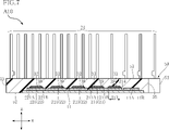
- FIG. 1 is a perspective view of a semiconductor device according to a first embodiment of the present disclosure
- FIG. 2 is a plan view of the semiconductor device shown in FIG. 1
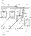
- FIG. FIG. 3 is a plan view corresponding to FIG. 2 and transparent through the sealing resin
- 2 is a bottom view of the semiconductor device shown in FIG. 1
- FIG. 2 is a front view of the semiconductor device shown in FIG. 1
- FIG. 2 is a right side view of the semiconductor device shown in FIG. 1
- FIG. FIG. 4 is a cross-sectional view along line VII-VII of FIG. 3
- FIG. 4 is a cross-sectional view along line VIII-VIII of FIG. 3
- 4 is a partially enlarged view of FIG. 3
- FIG. 10 is a cross-sectional view along line XX of FIG. 9;
- FIG. 10 is a cross-sectional view along line XI-XI of FIG. 9;
- FIG. 10 is a cross-sectional view along line XI-XI of FIG. 9;
- FIG. 10 is a cross-sectional view along line XI-XI of FIG. 9;
- FIG. 10 is a partially enlarged plan view of a semiconductor device according to a first modification of the first embodiment of the present disclosure, corresponding to FIG. 9;
- FIG. 10 is a partially enlarged plan view of a semiconductor device according to a second modification of the first embodiment of the present disclosure, corresponding to FIG. 9;
- FIG. 10 is a partially enlarged plan view of a semiconductor device according to a second modification of the first embodiment of the present disclosure, corresponding to FIG. 9;
- FIG. 9 is a partially enlarged plan view of a semiconductor device according to a second modification of the first embodiment of the present disclosure, corresponding
- FIG. 10 is a partially enlarged plan view of a semiconductor device according to a third modification of the first embodiment of the present disclosure, corresponding to FIG. 9;
- FIG. 10 is a partially enlarged plan view of a semiconductor device according to a fourth modification of the first embodiment of the present disclosure, corresponding to FIG. 9;
- FIG. 10 is a partially enlarged plan view of a semiconductor device according to a fifth modification of the first embodiment of the present disclosure, corresponding to FIG. 9;
- FIG. 4 is a plan view of a semiconductor device according to a second embodiment of the present disclosure, which is transparent through a sealing resin;
- FIG. 20 is a partially enlarged view of FIG. 19;
- FIG. 11 is a plan view of a semiconductor device according to a third embodiment of the present disclosure, which is transparent through a sealing resin;
- FIG. 11 is a plan view of a semiconductor device according to a fourth embodiment of the present disclosure, which is transparent through a sealing resin;
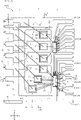
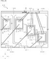
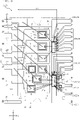
- FIG. 1 A semiconductor device A10 according to the first embodiment of the present disclosure will be described with reference to FIGS. 1 to 13.
- FIG. The semiconductor device A10 includes a substrate 11, an underlying layer 12, a bonding layer 13, a first lead 21, a plurality of second leads 22, a plurality of third leads 23, a plurality of first semiconductor elements 31, and a plurality of second semiconductor elements 32. , a conductive bonding layer 39 , a plurality of first wires 41 , a plurality of second wires 42 , and a sealing resin 50 .
- the semiconductor device A10 includes a plurality of driver leads 24, a first driver 33, a second driver 34, a plurality of diodes 35, a plurality of third wires 43, a plurality of fourth wires 44, a plurality of fifth wires 45, a plurality of A sixth wire 46 and a dummy lead 60 are provided.
- FIG. 3 is transparent through the sealing resin 50 for convenience of understanding.
- the permeated sealing resin 50 is indicated by an imaginary line (chain double-dashed line).
- the VII-VII line and the VIII-VIII line are indicated by one-dot chain lines.
- the thickness direction of the substrate 11 is called "thickness direction z" for convenience.
- a direction perpendicular to the thickness direction z is called a “first direction x”.
- a direction orthogonal to both the thickness direction z and the first direction x is called a "second direction y”.
- the semiconductor device A 10 converts the DC power supply voltage applied to the first lead 21 and the third lead 23 into AC power by the plurality of first semiconductor elements 31 and the plurality of second semiconductor elements 32 .
- the converted AC power is output from the plurality of second leads 22 as three phases (U phase, V phase, W phase) with different phases.
- the semiconductor device A10 since the semiconductor device A10 includes the first driver 33 that drives the plurality of first semiconductor elements 31 and the second driver 34 that drives the plurality of second semiconductor elements 32, the semiconductor device A10 is an IPM (Intelligent Power Module). be.
- the semiconductor device A10 is used, for example, in a power supply circuit for driving a three-phase AC motor.
- the substrate 11 supports a first lead 21 and a plurality of second leads 22, as shown in FIGS.
- the substrate 11 has electrical insulation.
- Substrate 11 is made of ceramics containing alumina (Al 2 O 3 ), for example.
- the material of the substrate 11 is preferably a material with relatively high thermal conductivity.
- substrate 11 has main surface 11A and back surface 11B. 11 A of main surfaces face the thickness direction z.
- the back surface 11B faces the side opposite to the main surface 11A in the thickness direction z.
- the substrate 11 is covered with a sealing resin 50 except for the back surface 11B.
- the first dimension D1 of the substrate 11 in the first direction x is greater than the second dimension D2 of the substrate 11 in the second direction y. Therefore, the first direction x corresponds to the long side direction of the substrate 11 .
- the underlying layer 12 is laminated on the main surface 11A of the substrate 11, as shown in FIG.
- the underlayer 12 contains a metal element.
- the metal element is silver (Ag).
- An example of the base layer 12 is a baked resinate silver paste applied to the main surface 11A.
- the bonding layer 13 is laminated on the base layer 12 as shown in FIG.
- the bonding layer 13 bonds the underlying layer 12 to the first lead 21 and the plurality of second leads 22 .
- the bonding layer 13 contains a metal element.
- the metal element is tin (Sn).
- Bonding layer 13 is, for example, lead-free solder containing an alloy of tin and antimony (Sb).
- the first lead 21, the plurality of second leads 22, and the plurality of third leads 23, along with the plurality of driver leads 24 and dummy leads 60, are configured from the same lead frame.
- the lead frame is copper (Cu) or a copper alloy. Therefore, the compositions of the first lead 21, the plurality of second leads 22, the plurality of third leads 23, the plurality of driver leads 24, and the dummy leads 60 contain copper (Cu). In other words, these leads contain copper.
- the first lead 21 is fixed onto the main surface 11A of the substrate 11, as shown in FIGS.
- the first lead 21 has a pad portion 211 and a terminal portion 212 .
- a plurality of first semiconductor elements 31 are mounted on the pad section 211 .
- the pad portion 211 has a mounting surface 211A and a facing surface 211B.
- the mounting surface 211A faces the same side as the main surface 11A in the thickness direction z.
- the facing surface 211B faces the side opposite to the mounting surface 211A in the thickness direction z.
- the facing surface 211B faces the main surface 11A. As shown in FIG. 10 , the facing surface 211B is in contact with the bonding layer 13 .
- the pad portion 211 is fixed to the main surface 11A via the underlying layer 12 and the bonding layer 13 .
- the pad portion 211 is covered with the sealing resin 50 .
- the terminal portion 212 is connected to the pad portion 211 . As shown in FIGS. 2, 4 and 5, a portion of the terminal portion 212 is exposed from the sealing resin 50.
- the terminal portion 212 corresponds to a P terminal (positive electrode) to which a DC power supply voltage to be converted is applied.
- the plurality of second leads 22 are positioned apart from the first leads 21 and fixed onto the main surface 11A of the substrate 11, as shown in FIGS.
- the plurality of second leads 22 are positioned next to the first leads 21 in the first direction x and arranged along the first direction x.
- Each of the multiple second leads 22 has a pad portion 221 and a terminal portion 222 .
- a plurality of second semiconductor elements 32 are individually mounted on the pad portions 221 of the plurality of second leads 22 .
- the area of the pad portion 221 is smaller than the area of the pad portion 211 of the first lead 21 when viewed in the thickness direction z.
- the pad portion 221 has a mounting surface 221A and a facing surface 221B.
- the mounting surface 221A faces the same side as the main surface 11A in the thickness direction z.
- the facing surface 221B faces the side opposite to the mounting surface 221A in the thickness direction z.
- the facing surface 221B faces the main surface 11A.
- the facing surface 221B is in contact with the bonding layer 13 .
- the pad portion 221 is fixed to the main surface 11A via the underlying layer 12 and the bonding layer 13 .
- the pad section 221 is covered with the sealing resin 50 .
- the terminal portion 222 is connected to the pad portion 221 . As shown in FIGS. 2, 4 and 5, a portion of the terminal portion 222 is exposed from the sealing resin 50.
- three-phase AC power is output from the terminal portions 212 of the plurality of second leads 22 .
- the plurality of third leads 23 are positioned apart from the first lead 21 and the plurality of second leads 22, as shown in FIG.
- the plurality of third leads 23 are located on the opposite side of the plurality of second leads 22 from the first leads 21 in the first direction x.
- the plurality of third leads 23 are supported not by the substrate 11 but by the sealing resin 50 . As shown in FIGS. 2, 4 and 5, a portion of each of the multiple third leads 23 is exposed from the sealing resin 50 .
- the plurality of third leads 23 are N terminals (negative electrodes) to which a DC power supply voltage to be converted is applied.
- the plurality of first semiconductor elements 31 are arranged on the mounting surface 211A of the pad portion 211 of the first lead 21, as shown in FIGS.
- the plurality of second semiconductor elements 32 are individually arranged on the mounting surface 221A of the pad portion 221 of the plurality of second leads 22, as shown in FIGS.
- the plurality of first semiconductor elements 31 and the plurality of second semiconductor elements 32 are all the same semiconductor element.
- the plurality of first semiconductor elements 31 and the plurality of second semiconductor elements 32 are, for example, MOSFETs (Metal-Oxide-Semiconductor Field-Effect Transistors).
- the MOSFET is of n-channel type and vertical structure.
- Each of the plurality of first semiconductor elements 31 and the plurality of second semiconductor elements 32 includes a compound semiconductor substrate.
- the compound semiconductor substrate contains silicon carbide (SiC).
- each of the plurality of first semiconductor elements 31 has a first electrode 311, a second electrode 312, a gate electrode 313 and a first edge 314.
- FIG. 10 the first electrode 311 faces the mounting surface 211A of the pad portion 211 of the first lead 21 .
- a voltage corresponding to power before being converted by the first semiconductor element 31 is applied to the first electrode 311 . That is, the first electrode 311 corresponds to the drain electrode of the first semiconductor element 31 .
- the second electrode 312 is located on the side opposite to the first electrode 311 in the thickness direction z.
- a voltage corresponding to the power converted by the first semiconductor element 31 is applied to the second electrode 312 . That is, the second electrode 312 corresponds to the source electrode of the first semiconductor element 31 .
- the second electrode 312 includes multiple metal plating layers.
- the second electrode 312 includes a nickel (Ni) plating layer and a gold (Au) plating layer laminated on the nickel plating layer.
- the second electrode 312 includes a nickel plating layer, a palladium (Pd) plating layer laminated on the nickel plating layer, and a gold plating layer laminated on the palladium plating layer, good.
- the gate electrode 313 is provided on the same side as the second electrode 312 in the thickness direction z and is located away from the second electrode 312 .
- a gate voltage for driving the first semiconductor element 31 is applied to the gate electrode 313 .
- the area of the gate electrode 313 is smaller than the area of the second electrode 312 when viewed in the thickness direction z.
- the first edge 314 extends along the second direction y when viewed in the thickness direction z.
- the first edge 314 includes a pair of sections spaced apart from each other in the first direction x.
- each of the plurality of second semiconductor elements 32 has a first electrode 321, a second electrode 322, a gate electrode 323 and a second edge 324.
- FIG. 10 the first electrode 321 faces the mounting surface 221A of one of the pad portions 221 of the plurality of second leads 22 .
- a voltage corresponding to power before being converted by the second semiconductor element 32 is applied to the first electrode 321 . That is, the first electrode 321 corresponds to the drain electrode of the second semiconductor element 32 .
- the second electrode 322 is located on the side opposite to the first electrode 321 in the thickness direction z.
- a voltage corresponding to the power converted by the second semiconductor element 32 is applied to the second electrode 322 . That is, the second electrode 322 corresponds to the source electrode of the second semiconductor element 32 .
- the second electrode 322 includes multiple metal plating layers.
- the second electrode 322 includes a nickel plating layer and a gold plating layer laminated on the nickel plating layer.
- the second electrode 322 may include a nickel plating layer, a palladium plating layer laminated on the nickel plating layer, and a gold plating layer laminated on the palladium plating layer.
- the gate electrode 323 is provided on the same side as the second electrode 322 in the thickness direction z and positioned away from the second electrode 322 .
- a gate voltage for driving the second semiconductor element 32 is applied to the gate electrode 323 .
- the area of the gate electrode 323 is smaller than the area of the second electrode 322 when viewed in the thickness direction z.
- the second edge 324 extends along the second direction y when viewed in the thickness direction z.
- the second edge 324 includes a pair of sections spaced apart from each other in the first direction x.
- the conductive bonding layer 39 bonds the mounting surface 211A of the pad portion 211 of the first lead 21 and the plurality of first semiconductor elements 31, as shown in FIG.
- the mounting surfaces 221A of the pad portions 221 of the plurality of second leads 22 and the plurality of second semiconductor elements 32 are individually bonded.
- the conductive bonding layer 39 is, for example, lead-free solder.
- the material of the conductive bonding layer 39 may be the same as the material of the bonding layer 13 .
- the first electrodes 311 of the plurality of first semiconductor elements 31 are bonded to the mounting surface 211A of the pad section 211 via the conductive bonding layer 39 .
- first electrodes 311 of the plurality of first semiconductor elements 31 are electrically connected to the first leads 21 .
- the first electrodes 321 of the plurality of second semiconductor elements 32 are individually bonded to the mounting surfaces 221A of the pad portions 221 of the plurality of second leads 22 via the conductive bonding layer 39 .
- the first electrodes 321 of the plurality of second semiconductor elements 32 are electrically connected to the plurality of second leads 22 individually.
- the plurality of first wires 41 are individually joined to the second electrodes 312 of the plurality of first semiconductor elements 31 and the terminal portions 222 of the plurality of second leads 22, as shown in FIG. Thereby, the second electrodes 312 of the plurality of first semiconductor elements 31 are electrically connected to the plurality of second leads 22 individually.
- the multiple first wires 41 contain aluminum (Al). Alternatively, the plurality of first wires 41 may contain copper.
- the plurality of second wires 42 are individually joined to the plurality of second electrodes 322 of the plurality of second semiconductor elements 32 and the plurality of third leads 23, as shown in FIG. Thereby, the second electrodes 322 of the plurality of second semiconductor elements 32 are electrically connected to the plurality of third leads 23 individually.
- the multiple second wires 42 contain aluminum. Alternatively, the plurality of second wires 42 may contain copper.
- the first leads 21, the plurality of first semiconductor elements 31, and the plurality of first wires 41 form a plurality of upper arm circuits.
- the plurality of second leads 22, the plurality of second semiconductor elements 32, the plurality of second wires 42, and the plurality of third leads 23 form a plurality of lower arm circuits. Therefore, the voltage applied to the gate electrode 313 of each of the plurality of first semiconductor elements 31 is relatively higher than the voltage applied to the gate electrode 323 of each of the plurality of second semiconductor elements 32 .
- the grounds of the plurality of lower arm circuits are different from each other.
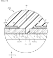
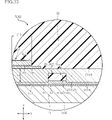
- the pad portion 211 of the first lead 21 includes a first region 213 and a second region 214.
- the first region 213 is a portion that overlaps with the plurality of first semiconductor elements 31 when viewed in the thickness direction z.
- the second region 214 is positioned apart from the plurality of first semiconductor elements 31 when viewed in the thickness direction z.
- the second region 214 extends along the second direction y.
- the dimension b in the first direction x of the second region 214 is smaller than the dimension B in the first direction x of each of the plurality of first semiconductor elements 31 .
- one side of the second region 214 in the second direction y reaches the peripheral edge 211C of the pad portion 211.
- the first edge 314 of any one of the plurality of first semiconductor elements 31 is located next to the second region 214 in the first direction x.
- the thickness t 2 of the second region 214 is less than the thickness t 1 of the first region 213 .
- the second area 214 is a slit.
- the slit penetrates the pad portion 211 of the first lead 21 in the thickness direction z.
- the second region 214 has an inner surface 214A facing the first direction x. Both the bonding layer 13 and the sealing resin 50 are in contact with the inner surface 214A.
- the second region 214 is a groove recessed from the mounting surface 211A of the pad portion 211 of the first lead 21.
- the second region 214 has an inner surface 214A and a bottom surface 214B.
- the bottom surface 214B is connected to the inner surface 214A and faces the same side as the mounting surface 211A in the thickness direction z.
- a sealing resin 50 is in contact with the inner side surface 214A and the bottom surface 214B.
- the second region 214 is a groove that is recessed from the facing surface 211B of the pad portion 211 of the first lead 21 .
- the second region 214 has an inner surface 214A and a bottom surface 214B.
- the bottom surface 214B of this example faces the same side as the opposing surface 211B in the thickness direction z.
- the bonding layer 13 is in contact with the inner side surface 214A.
- a sealing resin 50 is in contact with the inner side surface 214A and the bottom surface 214B.
- the plurality of driver leads 24 are connected to the substrate 11 in the second direction y. 23 is located on the opposite side.
- the plurality of driver leads 24 are supported not by the substrate 11 but by the sealing resin 50 , like the plurality of third leads 23 .
- a portion of each of the plurality of driver leads 24 is exposed from the sealing resin 50.
- the plurality of driver leads 24 includes a pad section 241 , a plurality of power supply sections 242 , a plurality of first control sections 243 , a plurality of second control sections 244 and a dummy section 245 .
- the pad section 241 has the first driver 33 and the second driver 34 mounted thereon. Further, the pad section 241 is used as the ground for the first driver 33 and the second driver 34 .
- the plurality of power supply units 242 are supplied with power that serves as a basis for gate voltages for driving the plurality of first semiconductor elements 31 . Electrical signals related to the control of the first driver 33 are input to and output from the plurality of first controllers 243 . Electrical signals related to the control of the second driver 34 are input to and output from the plurality of second control units 244 .
- the dummy section 245 does not conduct to both the first driver 33 and the second driver 34 .
- the first driver 33 is joined to the pad portion 241 via the conductive joining layer 39, as shown in FIG.
- the first driver 33 is an LSI. As shown in FIG. 3, the first driver 33 is positioned closer to the pad portion 211 of the first lead 21 than the second driver 34 is.
- the first driver 33 applies a gate voltage to the gate electrodes 313 of the plurality of first semiconductor elements 31 .
- the second driver 34 is bonded to the pad section 241 via the conductive bonding layer 39, like the first driver 33.
- the second driver 34 is an LSI. As shown in FIG. 3, the second driver 34 is positioned closer to the pad portions 221 of the plurality of second leads 22 than the first driver 33 is.
- the second driver 34 applies a gate voltage to the gate electrodes 323 of the plurality of second semiconductor elements 32 .
- the plurality of diodes 35 are individually joined to the plurality of power supply units 242 via the conductive joining layer 39, as shown in FIG.
- the multiple diodes 35 prevent a reverse bias from being applied to the multiple power supply units 242 as the multiple first semiconductor elements 31 are driven.
- the plurality of third wires 43 are connected to the first driver 33 and the second electrodes 312 and gate electrodes 313 of the plurality of first semiconductor elements 31, as shown in FIG. Thereby, a gate voltage is applied from the first driver 33 to the gate electrodes 313 of the plurality of first semiconductor elements 31 . At the same time, the ground of the gate voltage is set in the first driver 33 .
- the plurality of third wires 43 contain gold, for example.
- the plurality of fourth wires 44 are connected to the second driver 34 and the gate electrodes 323 of the plurality of second semiconductor elements 32, as shown in FIG. Thereby, a gate voltage is applied from the second driver 34 to the gate electrodes 323 of the plurality of second semiconductor elements 32 .
- the plurality of fourth wires 44 contain gold, for example.
- the plurality of fifth wires 45 are connected to the first driver 33, the pad section 241, the plurality of power supply sections 242, the plurality of diodes 35, and the plurality of first control sections 243, as shown in FIG. .
- the pad section 241 , the plurality of power supply sections 242 , the plurality of diodes 35 , and the plurality of first control sections 243 are electrically connected to the first driver 33 .
- the plurality of fifth wires 45 contain gold, for example.
- the plurality of sixth wires 46 are connected to the second driver 34, the pad section 241, and the plurality of second control sections 244, as shown in FIG. Thereby, the pad section 241 and the plurality of second control sections 244 are electrically connected to the second driver 34 .
- the multiple sixth wires 46 contain gold, for example.
- the dummy lead 60 is positioned apart from the substrate 11 when viewed in the thickness direction z, as shown in FIG.
- the dummy lead 60 is located on the side opposite to the terminal portion 222 of the plurality of second leads 22 with respect to the terminal portion 212 of the first lead 21 in the first direction x.
- part of the dummy lead 60 is exposed from the sealing resin 50.
- FIG. 1 shows that
- the sealing resin 50 is applied to each of the plurality of first semiconductor elements 31, the plurality of second semiconductor elements 32, the first leads 21, and the plurality of second leads 22. Each part is covered.
- the sealing resin 50 has electrical insulation.
- Sealing resin 50 is made of a material containing, for example, black epoxy resin.
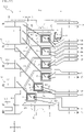
- the sealing resin 50 has a top surface 51 , a bottom surface 52 , a pair of first side surfaces 53 , a pair of second side surfaces 54 and a pair of recesses 55 .
- the top surface 51 faces the same side as the major surface 11A of the substrate 11 in the thickness direction z.
- the bottom surface 52 faces away from the top surface 51 in the thickness direction z.
- the back surface 11B of the substrate 11 is exposed from the bottom surface 52.
- the pair of first side surfaces 53 are positioned apart from each other in the first direction x.
- Each of the pair of first side surfaces 53 is connected to the top surface 51 and the bottom surface 52 .
- the pair of second side surfaces 54 are positioned apart from each other in the second direction y.
- Each of the pair of second side surfaces 54 is connected to the top surface 51 and the bottom surface 52 .
- the terminal portion 212 of the first lead 21, the terminal portion 222 of the plurality of second leads 22, the plurality of third leads 23, and the dummy leads 60 are connected. Some are exposed.
- a portion of each of the plurality of driver leads 24 is exposed from the other second side surface 54 of the pair of second side surfaces 54 .
- the pair of recesses 55 are recessed from the pair of first side surfaces 53 in the first direction x.
- the pair of recesses 55 extends from the top surface 51 to the bottom surface 52 in the thickness direction z.
- the pair of recesses 55 ensures a longer creepage distance of the sealing resin 50 from the terminal portion 212 of the first lead 21 and any one of the plurality of third leads 23 to any one of the plurality of driver leads 24. . This is suitable for improving the withstand voltage of the semiconductor device A10.
- FIG. 14 These modified examples differ in the configuration of the second region 214 of the pad portion 211 of the first lead 21 from the configuration of the semiconductor device A10.
- a semiconductor device A11 which is a first modification of the semiconductor device A10, will be described with reference to FIG.
- the second region 214 has a narrow portion 214C.
- the narrow portion 214C is one of the first semiconductor elements 31 when viewed in the thickness direction z. It is positioned between the first edge 314 and the first edge 314 of the other first semiconductor element 31 .
- a semiconductor device A12 which is a second modification of the semiconductor device A10, will be described with reference to FIG.
- the second region 214 is included in the peripheral edge 211C of the pad portion 211. As shown in FIG. Therefore, both sides of the second region 214 in the second direction y are closed by other regions of the pad section 211 .
- a semiconductor device A13 which is a third modification of the semiconductor device A10, will be described with reference to FIG.
- the second region 214 is included in the peripheral edge 211C of the pad portion 211. As shown in FIG. Further, the second region 214 has a narrow portion 214C.
- a semiconductor device A14 which is a fourth modification of the semiconductor device A10, will be described with reference to FIG.
- the second region 214 includes two sections.
- One of the two sections has a narrow portion 214C.
- the lengths L1 and L2 of the two sections are equal to each other. However, as long as one of the two sections has the narrow portion 214C, the lengths L1 and L2 of the two sections may be different from each other.
- a semiconductor device A15 which is a fifth modification of the semiconductor device A10, will be described with reference to FIG.
- the second region 214 includes two sections. Each of the two sections has a narrow portion 214C.
- the lengths L1 and L2 of the two sections are different from each other. However, as long as each of the two sections has a narrow portion 214C, the lengths L1 and L2 of the two sections may be equal to each other.
- the semiconductor device A10 includes a substrate 11 and first leads 21 fixed on the main surface 11A.
- the dimension of the substrate 11 in the first direction x (first dimension D1 shown in FIG. 3) is larger than the dimension of the substrate 11 in the second direction y (second dimension D2 shown in FIG. 3).
- the first lead 21 includes a first region 213 overlapping the first semiconductor element 31 when viewed in the thickness direction z, and a second region 214 located away from the first semiconductor element 31 when viewed in the thickness direction z. . At least a portion of the second region 214 extends along the second direction y.
- the thickness t2 of the second region 214 is smaller than the thickness t1 of the first region 213. As shown in FIG.
- both the expansion and contraction amounts of the substrate 11 and the first leads 21 are greater in the first direction x than in the second direction y. become large. Therefore, the thermal strain at the interface between the substrate 11 and the first lead 21 caused by the difference in coefficient of linear expansion is larger in the first direction x than in the second direction y. Therefore, according to the configuration of the semiconductor device A10, the second region 214 disperses the component of the thermal strain in the first direction x. As a result, the concentration of thermal strain at the interface between the substrate 11 and the first lead 21 is relaxed, so that the maximum thermal stress acting on the substrate 11 due to the thermal strain is reduced. Therefore, according to the semiconductor device A10, it is possible to reduce the concentration of thermal stress acting on the substrate 11 to which the lead (first lead 21) is fixed.
- the second region 214 include a slit shown in FIG. 11, a groove recessed from the mounting surface 211A of the pad portion 211 of the first lead 21 shown in FIG. 12, and a groove recessed from the facing surface 211B of the pad portion 211 shown in FIG. Either is fine. If the second region 214 takes any of the specific examples of the slit shown in FIG. 11 and the groove recessed from the facing surface 211B shown in FIG. come into contact with As a result, since the bonding layer 13 has an anchoring effect with respect to the first lead 21 , the bonding strength of the first lead 21 to the substrate 11 can be improved. Furthermore, it is assumed that the second region 214 has either the slit shown in FIG.
- the first semiconductor element 31 has a first edge 314 extending along the second direction y when viewed in the thickness direction z.
- the first edge 314 is located next to the second region 214 in the first direction x.
- the coefficient of linear expansion of the semiconductor substrate included in the first semiconductor element 31 is smaller than the coefficient of linear expansion of the first lead 21 .
- the semiconductor device A10 includes two first semiconductor elements 31 spaced apart from each other in the second direction y.
- the second region 214 is a narrow portion located between the first edge 314 of one first semiconductor element 31 and the first edge 314 of the other first semiconductor element 31. 214C.
- the first regions 213 of the first leads 21 located on both sides of the second region 214 in the first direction x are sandwiched between the substrate 11 and the two first semiconductor elements 31 in the thickness direction z.
- the semiconductor device A10 further includes an underlying layer 12 laminated on the main surface 11A of the substrate 11. As shown in FIG.
- the bonding layer 13 bonds the underlying layer 12 and the first lead 21 .
- the underlying layer 12 and the bonding layer 13 contain a metal element. This increases the affinity of the bonding layer 13 with respect to the base layer 12, so that the bonding strength of the first lead 21 with respect to the substrate 11 can be improved.
- a configuration in which the underlying layer 12 contains silver and the bonding layer 13 contains tin is preferable for increasing the affinity of the bonding layer 13 for the underlying layer 12 .
- the semiconductor device A10 further includes a sealing resin 50 that covers parts of each of the substrate 11 and the first leads 21 and the first semiconductor element 31 .
- the sealing resin 50 is in contact with the second region 214 .
- the sealing resin 50 has an anchoring effect. Thereby, the bonding strength of the sealing resin 50 to the first lead 21 can be improved.
- the substrate 11 has a back surface 11B facing away from the main surface 11A in the thickness direction z. Back surface 11B is exposed from sealing resin 50 . As a result, it is possible to improve the heat dissipation of the semiconductor device A10.
- FIG. 19 is transparent through the sealing resin 50 for convenience of understanding.
- the permeated sealing resin 50 is indicated by imaginary lines.
- the semiconductor device A20 differs from the above-described semiconductor device A10 in that dummy elements 36 are provided.
- the dummy element 36 is arranged on the mounting surface 211A of the pad portion 211 of the first lead 21. As shown in FIG. The dummy element 36 is located away from the second region 214 . Further, the dummy element 36 is positioned on the side of the second region 214 in the first direction x where any one of the plurality of first semiconductor elements 31 is arranged.
- the dummy element 36 is bonded to the mounting surface 211A of the pad section 211 via the conductive bonding layer 39.
- Dummy element 36 is, for example, a diode. It does not matter whether or not the dummy element 36 is electrically connected to the first lead 21 .
- the coefficient of linear expansion of the semiconductor substrate included in the dummy element 36 is smaller than the coefficient of linear expansion of the first lead 21 .
- the coefficient of linear expansion of the semiconductor substrate is preferably a value relatively close to the coefficient of linear expansion of each semiconductor substrate of the plurality of first semiconductor elements 31 .
- the area of the dummy element 36 is relatively close to the area of each of the plurality of first semiconductor elements 31 when viewed in the thickness direction z.
- the dummy element 36 is positioned next to any one of the plurality of first semiconductor elements 31 in the second direction y.
- the semiconductor device A20 includes a substrate 11 and first leads 21 fixed on the main surface 11A.
- the dimension of the substrate 11 in the first direction x (first dimension D1 shown in FIG. 3) is larger than the dimension of the substrate 11 in the second direction y (second dimension D2 shown in FIG. 3).
- the first lead 21 includes a first region 213 overlapping the first semiconductor element 31 when viewed in the thickness direction z, and a second region 214 located away from the first semiconductor element 31 when viewed in the thickness direction z. . At least a portion of the second region 214 extends along the second direction y.
- the thickness t2 of the second region 214 is smaller than the thickness t1 of the first region 213.
- the semiconductor device A20 can also reduce the concentration of thermal stress acting on the substrate 11 to which the leads (first leads 21) are fixed.
- the semiconductor device A20 further includes a dummy element 36 arranged on the mounting surface 211A of the first lead 21 and positioned away from the second region 214. As shown in FIG. The dummy element 36 is located on the side where the first semiconductor element 31 is arranged with respect to the second region 214 in the first direction x. As a result, the first lead 21 is sandwiched between the substrate 11 and the first semiconductor element 31 and the dummy element 36 in the thickness direction z. Furthermore, the linear expansion coefficient of each of the semiconductor substrate included in the first semiconductor element 31 and the semiconductor substrate included in the dummy element 36 is smaller than the linear expansion coefficient of the first lead 21 .
- the dummy element 36 is positioned next to the first semiconductor element 31 in the second direction y.
- the thermal expansion and contraction of the first lead 21 by the substrate 11, the first semiconductor element 31 and the dummy element 36 are more strongly restrained in the first direction x than in the second direction y. Therefore, of the thermal strain at the interface between the substrate 11 and the first lead 21, the component of the thermal strain in the first direction x is greatly reduced. Therefore, the maximum thermal stress acting on the substrate 11 can be effectively reduced.
- FIG. 21 is transparent through the sealing resin 50 for convenience of understanding.
- the permeated sealing resin 50 is indicated by imaginary lines.
- the configuration of the first lead 21, the plurality of second leads 22, and the third lead 23 of the semiconductor device A30 is different from that of the semiconductor device A10 described above. Furthermore, the semiconductor device A30 is configured without the dummy lead 60 .
- each pad portion 221 of the plurality of second leads 22 has a base portion 221C and an oblique portion 221D. Any one of the plurality of second semiconductor elements 32 is mounted on the base portion 221C.
- the oblique portion 221D connects the base portion 221C and the terminal portion 222 of the second lead 22 .
- the oblique portion 221D is inclined with respect to the second direction y.
- the peripheral edge 211C positioned adjacent to the oblique portion 221D of the second lead 22 is oblique to the second direction y. It is inclined in the same direction as the portion 221D.
- the third lead 23 is a single member.
- a plurality of second wires 42 are connected to the third lead 23 . Therefore, in the semiconductor device A30, the plurality of lower arm circuits have a common ground.
- the semiconductor device A30 includes a substrate 11 and first leads 21 fixed on the main surface 11A.
- the dimension of the substrate 11 in the first direction x (first dimension D1 shown in FIG. 3) is larger than the dimension of the substrate 11 in the second direction y (second dimension D2 shown in FIG. 3).
- the first lead 21 includes a first region 213 overlapping the first semiconductor element 31 when viewed in the thickness direction z, and a second region 214 located away from the first semiconductor element 31 when viewed in the thickness direction z. . At least a portion of the second region 214 extends along the second direction y.
- the thickness t2 of the second region 214 is smaller than the thickness t1 of the first region 213.
- the semiconductor device A30 can also reduce the concentration of thermal stress acting on the substrate 11 to which the leads (first leads 21) are fixed.
- FIG. 22 is transparent through the sealing resin 50 for convenience of understanding.
- the permeated sealing resin 50 is indicated by imaginary lines.
- the semiconductor device A40 includes a plurality of first gate terminals 25, a plurality of second gate terminals 26, a plurality of first detection terminals 27, a plurality of second detection terminals 28, and a pair of temperature sensors instead of the plurality of driver leads 24.
- a detection terminal 29 is provided. As shown in FIG. 22, these terminals are opposite to the terminal portion 212 of the first lead 21, the terminal portion 222 of the plurality of second leads 22, and the third lead 23 with respect to the substrate 11 in the second direction y. side and arranged along the first direction x. A portion of each of these terminals is exposed from one second side surface 54 of the sealing resin 50 .
- These terminals, together with the first lead 21, the plurality of second leads 22, and the third lead 23, are constructed from the same lead frame.
- the semiconductor device A40 includes a thermistor 37 instead of the first driver 33, the second driver 34, and the plurality of diodes 35.
- FIG. These configurations are different from the semiconductor device A30 described above. Therefore, the semiconductor device A40 is not an IPM but a general power module. However, the semiconductor device A40 is also configured to output three-phase AC power from the terminal portions 222 of the plurality of second leads 22 .
- the multiple first gate terminals 25 are located closer to the pad section 211 of the first lead 21 than the multiple second gate terminals 26 are.
- the plurality of first gate terminals 25 are fixed to the main surface 11A of the substrate 11 via the underlying layer 12 and the bonding layer 13 .
- the plurality of third wires 43 are individually connected to the plurality of first gate terminals 25 and the gate electrodes 313 of the plurality of first semiconductor elements 31 .
- each of the plurality of first gate terminals 25 is electrically connected to the gate electrode 313 of one of the plurality of first semiconductor elements 31 .
- a gate voltage for driving the plurality of first semiconductor elements 31 is applied to the plurality of first gate terminals 25 .
- the plurality of second gate terminals 26 are positioned closer to the pad portions 221 of the plurality of second leads 22 than the plurality of first gate terminals 25 .
- a plurality of second gate terminals 26 are fixed to main surface 11A of substrate 11 via base layer 12 and bonding layer 13 .
- the multiple fourth wires 44 are individually connected to the multiple second gate terminals 26 and the gate electrodes 323 of the multiple second semiconductor elements 32 .
- each of the plurality of second gate terminals 26 is electrically connected to the gate electrode 323 of one of the plurality of second semiconductor elements 32 .
- a gate voltage for driving the plurality of second semiconductor elements 32 is applied to the plurality of second gate terminals 26 .
- each of the plurality of first detection terminals 27 is positioned next to one of the plurality of second gate terminals 26 in the first direction x.
- the multiple first detection terminals 27 are fixed to the main surface 11A of the substrate 11 via the base layer 12 and the bonding layer 13 .
- the multiple third wires 43 are individually connected to the multiple first detection terminals 27 and the multiple second electrodes 312 of the multiple first semiconductor elements 31 .
- each of the plurality of first detection terminals 27 is electrically connected to the second electrode 312 of one of the plurality of first semiconductor elements 31 .
- a voltage having the same potential as that applied to the second electrode 312 of one of the first semiconductor elements 31 is applied to each of the plurality of first detection terminals 27 .
- each of the plurality of second detection terminals 28 is positioned next to one of the plurality of second gate terminals 26 in the first direction x.
- the multiple second detection terminals 28 are fixed to the main surface 11A of the substrate 11 via the base layer 12 and the bonding layer 13 .
- the plurality of fourth wires 44 are individually connected to the plurality of second detection terminals 28 and the second electrodes 322 of the plurality of second semiconductor elements 32 .
- each of the plurality of second detection terminals 28 is electrically connected to the second electrode 322 of one of the plurality of second semiconductor elements 32 .
- a voltage having the same potential as the voltage applied to the second electrode 322 of one of the plurality of second semiconductor elements 32 is applied to each of the plurality of second detection terminals 28 .
- the pair of temperature detection terminals 29 are located on the opposite side of the substrate 11 from the third lead 23 in the second direction y.
- a pair of temperature detection terminals 29 are joined to wiring 61 arranged on the main surface 11A of the substrate 11 .
- the thermistor 37 is joined to the wiring 61 . Therefore, the pair of temperature detection terminals 29 are electrically connected to the thermistor 37 via the wiring 61 . Accordingly, by applying a voltage to the pair of temperature detection terminals 29, the temperature of the substrate 11 during use of the semiconductor device A40 can be detected.
- the semiconductor device A40 includes a substrate 11 and first leads 21 fixed on the main surface 11A.
- the dimension of the substrate 11 in the first direction x (first dimension D1 shown in FIG. 3) is larger than the dimension of the substrate 11 in the second direction y (second dimension D2 shown in FIG. 3).
- the first lead 21 includes a first region 213 overlapping the first semiconductor element 31 when viewed in the thickness direction z, and a second region 214 located away from the first semiconductor element 31 when viewed in the thickness direction z. . At least a portion of the second region 214 extends along the second direction y.
- the thickness t2 of the second region 214 is smaller than the thickness t1 of the first region 213.
- the semiconductor device A40 can also reduce the concentration of thermal stress acting on the substrate 11 to which the leads (first leads 21) are fixed.
- Appendix 1 a substrate having a main surface facing the thickness direction; a first lead having a mounting surface facing the same side as the principal surface in the thickness direction and fixed onto the principal surface; a first semiconductor element disposed on the mounting surface; a dimension of the substrate in a first direction orthogonal to the thickness direction is larger than a dimension of the substrate in a second direction orthogonal to the thickness direction and the first direction;
- the first lead includes a first region overlapping with the first semiconductor element when viewed in the thickness direction, and a first region separated from the first semiconductor element when viewed in the thickness direction. a second region extending along two directions; The semiconductor device, wherein the thickness of the second region is smaller than the thickness of the first region.
- Appendix 2 The semiconductor device according to appendix 1, wherein one side of the second region in the second direction reaches a peripheral edge of the first lead.
- Appendix 3. The first semiconductor element has a first edge extending along the second direction when viewed in the thickness direction, 3.
- the semiconductor device according to appendix 1 or 2 wherein the first edge is positioned next to the second region in the first direction when viewed in the thickness direction.
- Appendix 4. further comprising two additional semiconductor elements spaced apart from each other in the second direction; 3.
- Appendix 5. 5 The semiconductor device according to appendix 1, wherein one side of the second region in the second direction reaches a peripheral edge of the first lead.
- Appendix 3. The first semiconductor element has a first edge extending along the second direction when viewed in the thickness direction, 3.
- the semiconductor device according to appendix 1 or 2 wherein the first edge is positioned next
- Appendix 13 The semiconductor device according to any one of appendices 1 to 12, wherein the first semiconductor element is electrically connected to the first lead.
- Appendix 14 a second lead fixed on the major surface and spaced apart from the first lead; a second semiconductor element disposed on the second lead and electrically connected to the second lead; 14. The semiconductor device according to appendix 13, wherein the second lead is electrically connected to the first semiconductor element.
- Appendix 15. further comprising a third lead spaced from the first lead and the second lead; 15. The semiconductor device according to appendix 14, wherein the third lead is electrically connected to the second semiconductor element.
- the semiconductor device according to any one of appendices 1 to 15, wherein the sealing resin is in contact with the second region.
- the substrate has a back surface facing away from the principal surface in the thickness direction, 17.
- A10, A20, A30, A40 Semiconductor device 11: Substrate 11A: Main surface 11B: Back surface 12: Base layer 13: Bonding layer 21: First lead 211: Pad portion 211A: Mounting surface 211B: Opposite surface 211C: Periphery 212: Terminal portion 213: First region 214: Second region 214A: Inner side surface 214B: Bottom surface 214C: Narrow portion 22: Second lead 221: Pad portion 221A: Mounting surface 221B: Opposing surface 221C: Base portion 221D: Oblique portion 222: Terminal section 23: Third lead 24: Driver lead 241: Pad section 242: Power supply section 243: First control section 244: Second control section 245: Dummy section 25: First gate terminal 26: Second gate terminal 27: Second 1 detection terminal 28: second detection terminal 29: temperature detection terminal 31: first semiconductor element 311: first electrode 312: second electrode 313: gate electrode 314: first edge 32: second semiconductor element 321: first Electrode 322: Second
Landscapes
- Structures Or Materials For Encapsulating Or Coating Semiconductor Devices Or Solid State Devices (AREA)
Priority Applications (4)
| Application Number | Priority Date | Filing Date | Title |
|---|---|---|---|
| CN202280009288.1A CN116686086A (zh) | 2021-02-03 | 2022-01-20 | 半导体装置 |
| JP2022579433A JPWO2022168618A1 (https=) | 2021-02-03 | 2022-01-20 | |
| DE112022000361.8T DE112022000361T5 (de) | 2021-02-03 | 2022-01-20 | Halbleiterbauelement |
| US18/272,103 US20240071875A1 (en) | 2021-02-03 | 2022-01-20 | Semiconductor device |
Applications Claiming Priority (2)
| Application Number | Priority Date | Filing Date | Title |
|---|---|---|---|
| JP2021015729 | 2021-02-03 | ||
| JP2021-015729 | 2021-02-03 |
Publications (1)
| Publication Number | Publication Date |
|---|---|
| WO2022168618A1 true WO2022168618A1 (ja) | 2022-08-11 |
Family
ID=82741446
Family Applications (1)
| Application Number | Title | Priority Date | Filing Date |
|---|---|---|---|
| PCT/JP2022/001961 Ceased WO2022168618A1 (ja) | 2021-02-03 | 2022-01-20 | 半導体装置 |
Country Status (5)
| Country | Link |
|---|---|
| US (1) | US20240071875A1 (https=) |
| JP (1) | JPWO2022168618A1 (https=) |
| CN (1) | CN116686086A (https=) |
| DE (1) | DE112022000361T5 (https=) |
| WO (1) | WO2022168618A1 (https=) |
Citations (5)
| Publication number | Priority date | Publication date | Assignee | Title |
|---|---|---|---|---|
| JP2002314030A (ja) * | 2001-04-12 | 2002-10-25 | Mitsubishi Electric Corp | 半導体装置 |
| JP2014207430A (ja) * | 2013-03-21 | 2014-10-30 | ローム株式会社 | 半導体装置 |
| JP2014216459A (ja) * | 2013-04-25 | 2014-11-17 | 三菱電機株式会社 | 半導体装置 |
| JP2016072417A (ja) * | 2014-09-30 | 2016-05-09 | ルネサスエレクトロニクス株式会社 | 半導体装置 |
| WO2020012957A1 (ja) * | 2018-07-12 | 2020-01-16 | ローム株式会社 | 半導体装置 |
Family Cites Families (45)
| Publication number | Priority date | Publication date | Assignee | Title |
|---|---|---|---|---|
| JP2670208B2 (ja) * | 1992-04-27 | 1997-10-29 | 京セラ株式会社 | 半導体素子収納用パッケージ |
| JP3617574B2 (ja) * | 1996-05-22 | 2005-02-09 | 株式会社ルネサステクノロジ | 多連多列リードフレームおよびそれを用いる半導体装置の製造方法 |
| JP4190250B2 (ja) * | 2002-10-24 | 2008-12-03 | 株式会社ルネサステクノロジ | 半導体装置 |
| JP2004349397A (ja) * | 2003-05-21 | 2004-12-09 | Sharp Corp | 半導体装置およびそれに用いられるリードフレーム |
| JP4426955B2 (ja) * | 2004-11-30 | 2010-03-03 | 株式会社ルネサステクノロジ | 半導体装置 |
| JP4705881B2 (ja) * | 2006-05-09 | 2011-06-22 | パナソニック株式会社 | リードフレーム及びそれを用いた半導体装置 |
| US7683477B2 (en) * | 2007-06-26 | 2010-03-23 | Infineon Technologies Ag | Semiconductor device including semiconductor chips having contact elements |
| JP4924411B2 (ja) | 2007-12-27 | 2012-04-25 | 三菱電機株式会社 | 電力半導体装置 |
| US8030743B2 (en) * | 2008-01-07 | 2011-10-04 | Fairchild Semiconductor Corporation | Semiconductor package with an embedded printed circuit board and stacked die |
| JP3146231U (ja) * | 2008-08-28 | 2008-11-06 | サンケン電気株式会社 | リードフレームおよび半導体装置 |
| JP4634498B2 (ja) * | 2008-11-28 | 2011-02-16 | 三菱電機株式会社 | 電力用半導体モジュール |
| JP5793995B2 (ja) * | 2011-06-28 | 2015-10-14 | トヨタ自動車株式会社 | リードフレーム、及び、パワーモジュール |
| JP2013258387A (ja) * | 2012-05-15 | 2013-12-26 | Rohm Co Ltd | パワーモジュール半導体装置 |
| WO2014185050A1 (ja) * | 2013-05-16 | 2014-11-20 | 富士電機株式会社 | 半導体装置 |
| JP6081903B2 (ja) * | 2013-11-29 | 2017-02-15 | サンケン電気株式会社 | 半導体装置 |
| JP2015220429A (ja) * | 2014-05-21 | 2015-12-07 | ローム株式会社 | 半導体装置 |
| FR3025691B1 (fr) * | 2014-09-08 | 2016-10-07 | Schneider Electric Ind Sas | Module electronique haute puissance et procede de fabrication d'un tel module |
| JP6263108B2 (ja) * | 2014-09-11 | 2018-01-17 | 株式会社日立製作所 | 半導体装置、並びにそれを用いたオルタネータ及び電力変換装置 |
| KR102178865B1 (ko) * | 2015-02-25 | 2020-11-18 | 한국전자통신연구원 | 고속 스위칭 성능을 갖는 캐스코드 타입의 스위치 회로 |
| US9972569B2 (en) * | 2016-04-12 | 2018-05-15 | General Electric Company | Robust low inductance power module package |
| JP6832094B2 (ja) * | 2016-08-05 | 2021-02-24 | ローム株式会社 | パワーモジュール及びモータ駆動回路 |
| JP6689708B2 (ja) * | 2016-08-10 | 2020-04-28 | ルネサスエレクトロニクス株式会社 | 電子装置 |
| DE102016119485A1 (de) * | 2016-10-12 | 2018-04-12 | Infineon Technologies Ag | Chipträger mit elektrisch leitfähiger Schicht, die sich über eine wärmeleitfähige dielektrische Sheet-Struktur hinaus erstreckt |
| US10600727B2 (en) * | 2016-10-16 | 2020-03-24 | Alpha And Omega Semiconductor (Cayman) Ltd. | Molded intelligent power module for motors |
| JP6853435B2 (ja) * | 2017-01-17 | 2021-03-31 | 三菱マテリアル株式会社 | パワーモジュールの製造方法 |
| JP2018170362A (ja) * | 2017-03-29 | 2018-11-01 | 株式会社東芝 | 半導体モジュール |
| JPWO2018235329A1 (ja) * | 2017-06-20 | 2020-04-16 | 住友電気工業株式会社 | 半導体装置 |
| JP2019012767A (ja) * | 2017-06-30 | 2019-01-24 | ルネサスエレクトロニクス株式会社 | 半導体モジュールの製造方法および半導体モジュール |
| EP3499560B1 (en) * | 2017-12-15 | 2021-08-18 | Infineon Technologies AG | Semiconductor module and method for producing the same |
| US10347571B1 (en) * | 2018-01-09 | 2019-07-09 | Macom Technology Solutions Holdings, Inc. | Intra-package interference isolation |
| US10896869B2 (en) * | 2018-01-12 | 2021-01-19 | Amkor Technology Singapore Holding Pte. Ltd. | Method of manufacturing a semiconductor device |
| CN111602240B (zh) * | 2018-03-02 | 2023-08-01 | 新电元工业株式会社 | 树脂封装型半导体装置 |
| JP6897869B2 (ja) * | 2018-04-18 | 2021-07-07 | 三菱電機株式会社 | 半導体モジュール |
| JP7077893B2 (ja) * | 2018-09-21 | 2022-05-31 | 株式会社デンソー | 半導体装置 |
| CN118213346A (zh) * | 2018-10-24 | 2024-06-18 | 罗姆股份有限公司 | 半导体装置 |
| JP7045975B2 (ja) * | 2018-11-20 | 2022-04-01 | 三菱電機株式会社 | 半導体装置およびその製造方法、ならびに電力変換装置 |
| US11901341B2 (en) * | 2018-11-26 | 2024-02-13 | Mitsubishi Electric Corporation | Semiconductor package and production method thereof, and semiconductor device |
| JP2020102523A (ja) * | 2018-12-21 | 2020-07-02 | トヨタ自動車株式会社 | 半導体モジュール製造方法 |
| JP7170614B2 (ja) * | 2019-09-18 | 2022-11-14 | 株式会社東芝 | 半導体装置 |
| JP7358921B2 (ja) * | 2019-11-08 | 2023-10-11 | 富士電機株式会社 | 半導体モジュール及び半導体モジュールの製造方法 |
| KR102703392B1 (ko) * | 2019-11-25 | 2024-09-04 | 현대자동차주식회사 | 전력모듈 및 전력모듈에 적용되는 기판 구조 |
| JP7729024B2 (ja) * | 2020-03-12 | 2025-08-26 | 富士電機株式会社 | 半導体装置の製造方法及び半導体装置 |
| DE212021000245U1 (de) * | 2020-04-17 | 2022-06-08 | Rohm Co., Ltd. | Halbleiterbauteil |
| JP7332528B2 (ja) * | 2020-04-17 | 2023-08-23 | 三菱電機株式会社 | 半導体装置および半導体装置の製造方法 |
| WO2021215294A1 (ja) * | 2020-04-22 | 2021-10-28 | ローム株式会社 | 半導体装置 |
-
2022
- 2022-01-20 JP JP2022579433A patent/JPWO2022168618A1/ja active Pending
- 2022-01-20 CN CN202280009288.1A patent/CN116686086A/zh active Pending
- 2022-01-20 DE DE112022000361.8T patent/DE112022000361T5/de active Pending
- 2022-01-20 US US18/272,103 patent/US20240071875A1/en active Pending
- 2022-01-20 WO PCT/JP2022/001961 patent/WO2022168618A1/ja not_active Ceased
Patent Citations (5)
| Publication number | Priority date | Publication date | Assignee | Title |
|---|---|---|---|---|
| JP2002314030A (ja) * | 2001-04-12 | 2002-10-25 | Mitsubishi Electric Corp | 半導体装置 |
| JP2014207430A (ja) * | 2013-03-21 | 2014-10-30 | ローム株式会社 | 半導体装置 |
| JP2014216459A (ja) * | 2013-04-25 | 2014-11-17 | 三菱電機株式会社 | 半導体装置 |
| JP2016072417A (ja) * | 2014-09-30 | 2016-05-09 | ルネサスエレクトロニクス株式会社 | 半導体装置 |
| WO2020012957A1 (ja) * | 2018-07-12 | 2020-01-16 | ローム株式会社 | 半導体装置 |
Also Published As
| Publication number | Publication date |
|---|---|
| CN116686086A (zh) | 2023-09-01 |
| DE112022000361T5 (de) | 2023-10-12 |
| US20240071875A1 (en) | 2024-02-29 |
| JPWO2022168618A1 (https=) | 2022-08-11 |
Similar Documents
| Publication | Publication Date | Title |
|---|---|---|
| JP7163054B2 (ja) | 半導体装置 | |
| WO2019239771A1 (ja) | 半導体モジュール | |
| WO2023162722A1 (ja) | 半導体装置および半導体モジュール | |
| WO2019235146A1 (ja) | 半導体モジュール | |
| JP2023010801A (ja) | 半導体装置 | |
| WO2023112662A1 (ja) | 半導体モジュールおよび半導体装置 | |
| CN110447099A (zh) | 半导体器件 | |
| JP2023088628A (ja) | 半導体装置 | |
| JP7365368B2 (ja) | 半導体装置 | |
| WO2025142335A1 (ja) | 半導体装置 | |
| WO2022168618A1 (ja) | 半導体装置 | |
| WO2024018790A1 (ja) | 半導体装置 | |
| WO2023149257A1 (ja) | 半導体装置 | |
| WO2023243278A1 (ja) | 半導体装置 | |
| WO2024029336A1 (ja) | 半導体装置 | |
| WO2023053874A1 (ja) | 半導体装置 | |
| WO2023120185A1 (ja) | 半導体装置 | |
| US20240250014A1 (en) | Semiconductor device | |
| JP2021040065A (ja) | 半導体装置の実装構造 | |
| US20230420321A1 (en) | Semiconductor device | |
| US20240047315A1 (en) | Semiconductor device | |
| WO2024106219A1 (ja) | 半導体装置 | |
| WO2023140046A1 (ja) | 半導体装置 | |
| WO2023218943A1 (ja) | 半導体装置 | |
| WO2023112723A1 (ja) | 半導体装置、および半導体装置の実装体 |
Legal Events
| Date | Code | Title | Description |
|---|---|---|---|
| 121 | Ep: the epo has been informed by wipo that ep was designated in this application |
Ref document number: 22749494 Country of ref document: EP Kind code of ref document: A1 |
|
| ENP | Entry into the national phase |
Ref document number: 2022579433 Country of ref document: JP Kind code of ref document: A |
|
| WWE | Wipo information: entry into national phase |
Ref document number: 202280009288.1 Country of ref document: CN |
|
| WWE | Wipo information: entry into national phase |
Ref document number: 18272103 Country of ref document: US |
|
| WWE | Wipo information: entry into national phase |
Ref document number: 112022000361 Country of ref document: DE |
|
| 122 | Ep: pct application non-entry in european phase |
Ref document number: 22749494 Country of ref document: EP Kind code of ref document: A1 |