WO2022004758A1 - 半導体モジュールおよび半導体モジュールの製造方法 - Google Patents
半導体モジュールおよび半導体モジュールの製造方法 Download PDFInfo
- Publication number
- WO2022004758A1 WO2022004758A1 PCT/JP2021/024649 JP2021024649W WO2022004758A1 WO 2022004758 A1 WO2022004758 A1 WO 2022004758A1 JP 2021024649 W JP2021024649 W JP 2021024649W WO 2022004758 A1 WO2022004758 A1 WO 2022004758A1
- Authority
- WO
- WIPO (PCT)
- Prior art keywords
- recesses
- semiconductor module
- connection portion
- chip connection
- chip
- Prior art date
- Legal status (The legal status is an assumption and is not a legal conclusion. Google has not performed a legal analysis and makes no representation as to the accuracy of the status listed.)
- Ceased
Links
Images































Classifications
-
- H—ELECTRICITY
- H10—SEMICONDUCTOR DEVICES; ELECTRIC SOLID-STATE DEVICES NOT OTHERWISE PROVIDED FOR
- H10W—GENERIC PACKAGES, INTERCONNECTIONS, CONNECTORS OR OTHER CONSTRUCTIONAL DETAILS OF DEVICES COVERED BY CLASS H10
- H10W70/00—Package substrates; Interposers; Redistribution layers [RDL]
- H10W70/40—Leadframes
- H10W70/479—Leadframes on or in insulating or insulated package substrates, interposers, or redistribution layers
-
- H—ELECTRICITY
- H10—SEMICONDUCTOR DEVICES; ELECTRIC SOLID-STATE DEVICES NOT OTHERWISE PROVIDED FOR
- H10W—GENERIC PACKAGES, INTERCONNECTIONS, CONNECTORS OR OTHER CONSTRUCTIONAL DETAILS OF DEVICES COVERED BY CLASS H10
- H10W72/00—Interconnections or connectors in packages
- H10W72/60—Strap connectors, e.g. thick copper clips for grounding of power devices
-
- H—ELECTRICITY
- H10—SEMICONDUCTOR DEVICES; ELECTRIC SOLID-STATE DEVICES NOT OTHERWISE PROVIDED FOR
- H10W—GENERIC PACKAGES, INTERCONNECTIONS, CONNECTORS OR OTHER CONSTRUCTIONAL DETAILS OF DEVICES COVERED BY CLASS H10
- H10W70/00—Package substrates; Interposers; Redistribution layers [RDL]
- H10W70/01—Manufacture or treatment
- H10W70/04—Manufacture or treatment of leadframes
- H10W70/047—Attaching leadframes to insulating supports, e.g. for tape automated bonding [TAB]
-
- H—ELECTRICITY
- H10—SEMICONDUCTOR DEVICES; ELECTRIC SOLID-STATE DEVICES NOT OTHERWISE PROVIDED FOR
- H10W—GENERIC PACKAGES, INTERCONNECTIONS, CONNECTORS OR OTHER CONSTRUCTIONAL DETAILS OF DEVICES COVERED BY CLASS H10
- H10W70/00—Package substrates; Interposers; Redistribution layers [RDL]
- H10W70/60—Insulating or insulated package substrates; Interposers; Redistribution layers
- H10W70/62—Insulating or insulated package substrates; Interposers; Redistribution layers characterised by their interconnections
- H10W70/65—Shapes or dispositions of interconnections
- H10W70/658—Shapes or dispositions of interconnections for devices provided for in groups H10D8/00 - H10D48/00
-
- H—ELECTRICITY
- H10—SEMICONDUCTOR DEVICES; ELECTRIC SOLID-STATE DEVICES NOT OTHERWISE PROVIDED FOR
- H10W—GENERIC PACKAGES, INTERCONNECTIONS, CONNECTORS OR OTHER CONSTRUCTIONAL DETAILS OF DEVICES COVERED BY CLASS H10
- H10W90/00—Package configurations
-
- H—ELECTRICITY
- H10—SEMICONDUCTOR DEVICES; ELECTRIC SOLID-STATE DEVICES NOT OTHERWISE PROVIDED FOR
- H10W—GENERIC PACKAGES, INTERCONNECTIONS, CONNECTORS OR OTHER CONSTRUCTIONAL DETAILS OF DEVICES COVERED BY CLASS H10
- H10W95/00—Packaging processes not covered by the other groups of this subclass
-
- H—ELECTRICITY
- H10—SEMICONDUCTOR DEVICES; ELECTRIC SOLID-STATE DEVICES NOT OTHERWISE PROVIDED FOR
- H10W—GENERIC PACKAGES, INTERCONNECTIONS, CONNECTORS OR OTHER CONSTRUCTIONAL DETAILS OF DEVICES COVERED BY CLASS H10
- H10W40/00—Arrangements for thermal protection or thermal control
- H10W40/20—Arrangements for cooling
- H10W40/25—Arrangements for cooling characterised by their materials
- H10W40/255—Arrangements for cooling characterised by their materials having a laminate or multilayered structure, e.g. direct bond copper [DBC] ceramic substrates
-
- H—ELECTRICITY
- H10—SEMICONDUCTOR DEVICES; ELECTRIC SOLID-STATE DEVICES NOT OTHERWISE PROVIDED FOR
- H10W—GENERIC PACKAGES, INTERCONNECTIONS, CONNECTORS OR OTHER CONSTRUCTIONAL DETAILS OF DEVICES COVERED BY CLASS H10
- H10W70/00—Package substrates; Interposers; Redistribution layers [RDL]
- H10W70/60—Insulating or insulated package substrates; Interposers; Redistribution layers
- H10W70/67—Insulating or insulated package substrates; Interposers; Redistribution layers characterised by their insulating layers or insulating parts
- H10W70/68—Shapes or dispositions thereof
- H10W70/685—Shapes or dispositions thereof comprising multiple insulating layers
-
- H—ELECTRICITY
- H10—SEMICONDUCTOR DEVICES; ELECTRIC SOLID-STATE DEVICES NOT OTHERWISE PROVIDED FOR
- H10W—GENERIC PACKAGES, INTERCONNECTIONS, CONNECTORS OR OTHER CONSTRUCTIONAL DETAILS OF DEVICES COVERED BY CLASS H10
- H10W72/00—Interconnections or connectors in packages
- H10W72/01—Manufacture or treatment
- H10W72/016—Manufacture or treatment of strap connectors
- H10W72/01651—Changing the shapes of strap connectors
-
- H—ELECTRICITY
- H10—SEMICONDUCTOR DEVICES; ELECTRIC SOLID-STATE DEVICES NOT OTHERWISE PROVIDED FOR
- H10W—GENERIC PACKAGES, INTERCONNECTIONS, CONNECTORS OR OTHER CONSTRUCTIONAL DETAILS OF DEVICES COVERED BY CLASS H10
- H10W72/00—Interconnections or connectors in packages
- H10W72/01—Manufacture or treatment
- H10W72/016—Manufacture or treatment of strap connectors
- H10W72/01661—Chemical or physical modification, e.g. by sintering or anodisation
-
- H—ELECTRICITY
- H10—SEMICONDUCTOR DEVICES; ELECTRIC SOLID-STATE DEVICES NOT OTHERWISE PROVIDED FOR
- H10W—GENERIC PACKAGES, INTERCONNECTIONS, CONNECTORS OR OTHER CONSTRUCTIONAL DETAILS OF DEVICES COVERED BY CLASS H10
- H10W72/00—Interconnections or connectors in packages
- H10W72/071—Connecting or disconnecting
- H10W72/073—Connecting or disconnecting of die-attach connectors
- H10W72/07331—Connecting techniques
- H10W72/07336—Soldering or alloying
-
- H—ELECTRICITY
- H10—SEMICONDUCTOR DEVICES; ELECTRIC SOLID-STATE DEVICES NOT OTHERWISE PROVIDED FOR
- H10W—GENERIC PACKAGES, INTERCONNECTIONS, CONNECTORS OR OTHER CONSTRUCTIONAL DETAILS OF DEVICES COVERED BY CLASS H10
- H10W72/00—Interconnections or connectors in packages
- H10W72/071—Connecting or disconnecting
- H10W72/073—Connecting or disconnecting of die-attach connectors
- H10W72/07351—Connecting or disconnecting of die-attach connectors characterised by changes in properties of the die-attach connectors during connecting
- H10W72/07352—Connecting or disconnecting of die-attach connectors characterised by changes in properties of the die-attach connectors during connecting changes in structures or sizes
-
- H—ELECTRICITY
- H10—SEMICONDUCTOR DEVICES; ELECTRIC SOLID-STATE DEVICES NOT OTHERWISE PROVIDED FOR
- H10W—GENERIC PACKAGES, INTERCONNECTIONS, CONNECTORS OR OTHER CONSTRUCTIONAL DETAILS OF DEVICES COVERED BY CLASS H10
- H10W72/00—Interconnections or connectors in packages
- H10W72/071—Connecting or disconnecting
- H10W72/073—Connecting or disconnecting of die-attach connectors
- H10W72/07351—Connecting or disconnecting of die-attach connectors characterised by changes in properties of the die-attach connectors during connecting
- H10W72/07354—Connecting or disconnecting of die-attach connectors characterised by changes in properties of the die-attach connectors during connecting changes in dispositions
-
- H—ELECTRICITY
- H10—SEMICONDUCTOR DEVICES; ELECTRIC SOLID-STATE DEVICES NOT OTHERWISE PROVIDED FOR
- H10W—GENERIC PACKAGES, INTERCONNECTIONS, CONNECTORS OR OTHER CONSTRUCTIONAL DETAILS OF DEVICES COVERED BY CLASS H10
- H10W72/00—Interconnections or connectors in packages
- H10W72/071—Connecting or disconnecting
- H10W72/076—Connecting or disconnecting of strap connectors
-
- H—ELECTRICITY
- H10—SEMICONDUCTOR DEVICES; ELECTRIC SOLID-STATE DEVICES NOT OTHERWISE PROVIDED FOR
- H10W—GENERIC PACKAGES, INTERCONNECTIONS, CONNECTORS OR OTHER CONSTRUCTIONAL DETAILS OF DEVICES COVERED BY CLASS H10
- H10W72/00—Interconnections or connectors in packages
- H10W72/071—Connecting or disconnecting
- H10W72/076—Connecting or disconnecting of strap connectors
- H10W72/07631—Techniques
- H10W72/07636—Soldering or alloying
-
- H—ELECTRICITY
- H10—SEMICONDUCTOR DEVICES; ELECTRIC SOLID-STATE DEVICES NOT OTHERWISE PROVIDED FOR
- H10W—GENERIC PACKAGES, INTERCONNECTIONS, CONNECTORS OR OTHER CONSTRUCTIONAL DETAILS OF DEVICES COVERED BY CLASS H10
- H10W72/00—Interconnections or connectors in packages
- H10W72/071—Connecting or disconnecting
- H10W72/076—Connecting or disconnecting of strap connectors
- H10W72/07651—Connecting or disconnecting of strap connectors characterised by changes in properties of the strap connectors during connecting
- H10W72/07653—Connecting or disconnecting of strap connectors characterised by changes in properties of the strap connectors during connecting changes in shapes
-
- H—ELECTRICITY
- H10—SEMICONDUCTOR DEVICES; ELECTRIC SOLID-STATE DEVICES NOT OTHERWISE PROVIDED FOR
- H10W—GENERIC PACKAGES, INTERCONNECTIONS, CONNECTORS OR OTHER CONSTRUCTIONAL DETAILS OF DEVICES COVERED BY CLASS H10
- H10W72/00—Interconnections or connectors in packages
- H10W72/30—Die-attach connectors
- H10W72/321—Structures or relative sizes of die-attach connectors
- H10W72/327—Multiple die-attach connectors having different sizes
-
- H—ELECTRICITY
- H10—SEMICONDUCTOR DEVICES; ELECTRIC SOLID-STATE DEVICES NOT OTHERWISE PROVIDED FOR
- H10W—GENERIC PACKAGES, INTERCONNECTIONS, CONNECTORS OR OTHER CONSTRUCTIONAL DETAILS OF DEVICES COVERED BY CLASS H10
- H10W72/00—Interconnections or connectors in packages
- H10W72/30—Die-attach connectors
- H10W72/341—Dispositions of die-attach connectors, e.g. layouts
- H10W72/347—Dispositions of multiple die-attach connectors
-
- H—ELECTRICITY
- H10—SEMICONDUCTOR DEVICES; ELECTRIC SOLID-STATE DEVICES NOT OTHERWISE PROVIDED FOR
- H10W—GENERIC PACKAGES, INTERCONNECTIONS, CONNECTORS OR OTHER CONSTRUCTIONAL DETAILS OF DEVICES COVERED BY CLASS H10
- H10W72/00—Interconnections or connectors in packages
- H10W72/30—Die-attach connectors
- H10W72/351—Materials of die-attach connectors
- H10W72/352—Materials of die-attach connectors comprising metals or metalloids, e.g. solders
-
- H—ELECTRICITY
- H10—SEMICONDUCTOR DEVICES; ELECTRIC SOLID-STATE DEVICES NOT OTHERWISE PROVIDED FOR
- H10W—GENERIC PACKAGES, INTERCONNECTIONS, CONNECTORS OR OTHER CONSTRUCTIONAL DETAILS OF DEVICES COVERED BY CLASS H10
- H10W72/00—Interconnections or connectors in packages
- H10W72/60—Strap connectors, e.g. thick copper clips for grounding of power devices
- H10W72/621—Structures or relative sizes of strap connectors
- H10W72/622—Multilayered strap connectors, e.g. having a coating on a lowermost surface of a core
-
- H—ELECTRICITY
- H10—SEMICONDUCTOR DEVICES; ELECTRIC SOLID-STATE DEVICES NOT OTHERWISE PROVIDED FOR
- H10W—GENERIC PACKAGES, INTERCONNECTIONS, CONNECTORS OR OTHER CONSTRUCTIONAL DETAILS OF DEVICES COVERED BY CLASS H10
- H10W72/00—Interconnections or connectors in packages
- H10W72/60—Strap connectors, e.g. thick copper clips for grounding of power devices
- H10W72/621—Structures or relative sizes of strap connectors
- H10W72/622—Multilayered strap connectors, e.g. having a coating on a lowermost surface of a core
- H10W72/623—Multilayered strap connectors, e.g. having a coating on a lowermost surface of a core characterised by the structures of the outermost layers, e.g. multilayered coatings
-
- H—ELECTRICITY
- H10—SEMICONDUCTOR DEVICES; ELECTRIC SOLID-STATE DEVICES NOT OTHERWISE PROVIDED FOR
- H10W—GENERIC PACKAGES, INTERCONNECTIONS, CONNECTORS OR OTHER CONSTRUCTIONAL DETAILS OF DEVICES COVERED BY CLASS H10
- H10W72/00—Interconnections or connectors in packages
- H10W72/60—Strap connectors, e.g. thick copper clips for grounding of power devices
- H10W72/631—Shapes of strap connectors
-
- H—ELECTRICITY
- H10—SEMICONDUCTOR DEVICES; ELECTRIC SOLID-STATE DEVICES NOT OTHERWISE PROVIDED FOR
- H10W—GENERIC PACKAGES, INTERCONNECTIONS, CONNECTORS OR OTHER CONSTRUCTIONAL DETAILS OF DEVICES COVERED BY CLASS H10
- H10W72/00—Interconnections or connectors in packages
- H10W72/60—Strap connectors, e.g. thick copper clips for grounding of power devices
- H10W72/631—Shapes of strap connectors
- H10W72/634—Cross-sectional shape
-
- H—ELECTRICITY
- H10—SEMICONDUCTOR DEVICES; ELECTRIC SOLID-STATE DEVICES NOT OTHERWISE PROVIDED FOR
- H10W—GENERIC PACKAGES, INTERCONNECTIONS, CONNECTORS OR OTHER CONSTRUCTIONAL DETAILS OF DEVICES COVERED BY CLASS H10
- H10W72/00—Interconnections or connectors in packages
- H10W72/60—Strap connectors, e.g. thick copper clips for grounding of power devices
- H10W72/641—Dispositions of strap connectors
- H10W72/645—Dispositions of strap connectors of outermost layers of multilayered strap connectors, e.g. coating being only on a part of a core
-
- H—ELECTRICITY
- H10—SEMICONDUCTOR DEVICES; ELECTRIC SOLID-STATE DEVICES NOT OTHERWISE PROVIDED FOR
- H10W—GENERIC PACKAGES, INTERCONNECTIONS, CONNECTORS OR OTHER CONSTRUCTIONAL DETAILS OF DEVICES COVERED BY CLASS H10
- H10W72/00—Interconnections or connectors in packages
- H10W72/60—Strap connectors, e.g. thick copper clips for grounding of power devices
- H10W72/641—Dispositions of strap connectors
- H10W72/646—Dispositions of strap connectors the connected ends being on auxiliary connecting means on bond pads, e.g. on a bump connector
-
- H—ELECTRICITY
- H10—SEMICONDUCTOR DEVICES; ELECTRIC SOLID-STATE DEVICES NOT OTHERWISE PROVIDED FOR
- H10W—GENERIC PACKAGES, INTERCONNECTIONS, CONNECTORS OR OTHER CONSTRUCTIONAL DETAILS OF DEVICES COVERED BY CLASS H10
- H10W72/00—Interconnections or connectors in packages
- H10W72/60—Strap connectors, e.g. thick copper clips for grounding of power devices
- H10W72/651—Materials of strap connectors
- H10W72/652—Materials of strap connectors comprising metals or metalloids, e.g. silver
-
- H—ELECTRICITY
- H10—SEMICONDUCTOR DEVICES; ELECTRIC SOLID-STATE DEVICES NOT OTHERWISE PROVIDED FOR
- H10W—GENERIC PACKAGES, INTERCONNECTIONS, CONNECTORS OR OTHER CONSTRUCTIONAL DETAILS OF DEVICES COVERED BY CLASS H10
- H10W72/00—Interconnections or connectors in packages
- H10W72/60—Strap connectors, e.g. thick copper clips for grounding of power devices
- H10W72/651—Materials of strap connectors
- H10W72/653—Materials of strap connectors not comprising solid metals or solid metalloids, e.g. polymers, ceramics or liquids
-
- H—ELECTRICITY
- H10—SEMICONDUCTOR DEVICES; ELECTRIC SOLID-STATE DEVICES NOT OTHERWISE PROVIDED FOR
- H10W—GENERIC PACKAGES, INTERCONNECTIONS, CONNECTORS OR OTHER CONSTRUCTIONAL DETAILS OF DEVICES COVERED BY CLASS H10
- H10W72/00—Interconnections or connectors in packages
- H10W72/60—Strap connectors, e.g. thick copper clips for grounding of power devices
- H10W72/651—Materials of strap connectors
- H10W72/655—Materials of strap connectors of outermost layers of multilayered strap connectors, e.g. material of a coating
-
- H—ELECTRICITY
- H10—SEMICONDUCTOR DEVICES; ELECTRIC SOLID-STATE DEVICES NOT OTHERWISE PROVIDED FOR
- H10W—GENERIC PACKAGES, INTERCONNECTIONS, CONNECTORS OR OTHER CONSTRUCTIONAL DETAILS OF DEVICES COVERED BY CLASS H10
- H10W72/00—Interconnections or connectors in packages
- H10W72/851—Dispositions of multiple connectors or interconnections
- H10W72/874—On different surfaces
- H10W72/886—Die-attach connectors and strap connectors
-
- H—ELECTRICITY
- H10—SEMICONDUCTOR DEVICES; ELECTRIC SOLID-STATE DEVICES NOT OTHERWISE PROVIDED FOR
- H10W—GENERIC PACKAGES, INTERCONNECTIONS, CONNECTORS OR OTHER CONSTRUCTIONAL DETAILS OF DEVICES COVERED BY CLASS H10
- H10W72/00—Interconnections or connectors in packages
- H10W72/90—Bond pads, in general
- H10W72/951—Materials of bond pads
- H10W72/952—Materials of bond pads comprising metals or metalloids, e.g. PbSn, Ag or Cu
-
- H—ELECTRICITY
- H10—SEMICONDUCTOR DEVICES; ELECTRIC SOLID-STATE DEVICES NOT OTHERWISE PROVIDED FOR
- H10W—GENERIC PACKAGES, INTERCONNECTIONS, CONNECTORS OR OTHER CONSTRUCTIONAL DETAILS OF DEVICES COVERED BY CLASS H10
- H10W74/00—Encapsulations, e.g. protective coatings
-
- H—ELECTRICITY
- H10—SEMICONDUCTOR DEVICES; ELECTRIC SOLID-STATE DEVICES NOT OTHERWISE PROVIDED FOR
- H10W—GENERIC PACKAGES, INTERCONNECTIONS, CONNECTORS OR OTHER CONSTRUCTIONAL DETAILS OF DEVICES COVERED BY CLASS H10
- H10W74/00—Encapsulations, e.g. protective coatings
- H10W74/10—Encapsulations, e.g. protective coatings characterised by their shape or disposition
-
- H—ELECTRICITY
- H10—SEMICONDUCTOR DEVICES; ELECTRIC SOLID-STATE DEVICES NOT OTHERWISE PROVIDED FOR
- H10W—GENERIC PACKAGES, INTERCONNECTIONS, CONNECTORS OR OTHER CONSTRUCTIONAL DETAILS OF DEVICES COVERED BY CLASS H10
- H10W74/00—Encapsulations, e.g. protective coatings
- H10W74/40—Encapsulations, e.g. protective coatings characterised by their materials
-
- H—ELECTRICITY
- H10—SEMICONDUCTOR DEVICES; ELECTRIC SOLID-STATE DEVICES NOT OTHERWISE PROVIDED FOR
- H10W—GENERIC PACKAGES, INTERCONNECTIONS, CONNECTORS OR OTHER CONSTRUCTIONAL DETAILS OF DEVICES COVERED BY CLASS H10
- H10W90/00—Package configurations
- H10W90/701—Package configurations characterised by the relative positions of pads or connectors relative to package parts
- H10W90/731—Package configurations characterised by the relative positions of pads or connectors relative to package parts of die-attach connectors
- H10W90/734—Package configurations characterised by the relative positions of pads or connectors relative to package parts of die-attach connectors between a chip and a stacked insulating package substrate, interposer or RDL
-
- H—ELECTRICITY
- H10—SEMICONDUCTOR DEVICES; ELECTRIC SOLID-STATE DEVICES NOT OTHERWISE PROVIDED FOR
- H10W—GENERIC PACKAGES, INTERCONNECTIONS, CONNECTORS OR OTHER CONSTRUCTIONAL DETAILS OF DEVICES COVERED BY CLASS H10
- H10W90/00—Package configurations
- H10W90/701—Package configurations characterised by the relative positions of pads or connectors relative to package parts
- H10W90/731—Package configurations characterised by the relative positions of pads or connectors relative to package parts of die-attach connectors
- H10W90/736—Package configurations characterised by the relative positions of pads or connectors relative to package parts of die-attach connectors between a chip and a stacked lead frame, conducting package substrate or heat sink
-
- H—ELECTRICITY
- H10—SEMICONDUCTOR DEVICES; ELECTRIC SOLID-STATE DEVICES NOT OTHERWISE PROVIDED FOR
- H10W—GENERIC PACKAGES, INTERCONNECTIONS, CONNECTORS OR OTHER CONSTRUCTIONAL DETAILS OF DEVICES COVERED BY CLASS H10
- H10W90/00—Package configurations
- H10W90/701—Package configurations characterised by the relative positions of pads or connectors relative to package parts
- H10W90/761—Package configurations characterised by the relative positions of pads or connectors relative to package parts of strap connectors
- H10W90/764—Package configurations characterised by the relative positions of pads or connectors relative to package parts of strap connectors between a chip and a stacked insulating package substrate, interposer or RDL
Definitions
- the present invention relates to a semiconductor module and a method for manufacturing a semiconductor module.
- Patent Document 1 WO2017 / 163583
- the semiconductor module may include an insulating circuit board having a circuit pattern formed on one surface thereof, a semiconductor chip mounted on the insulating circuit board, and a wiring portion for electrically connecting the semiconductor chip and the circuit pattern.
- the wiring portion may have a chip connection portion for connecting to the semiconductor chip.
- the surface of the chip connection may have a plurality of recesses.
- the surface of the chip connection portion may have a flat surface portion arranged between the two recesses.
- the second aspect of the present invention provides a semiconductor module.
- the semiconductor module includes an insulated circuit board having a circuit pattern formed on one surface, a semiconductor chip mounted on the insulated circuit board, and a rough surface region having a developed area ratio of 0.2 or more on at least a part of the surface. It may be provided with a wiring portion for connecting the semiconductor chip and the circuit pattern, and a resin package for protecting the semiconductor chip.
- a third aspect of the present invention provides a semiconductor module.
- the semiconductor module includes an insulated circuit board having a circuit pattern formed on one surface, a semiconductor chip mounted on the insulated circuit board, a wiring portion connecting the semiconductor chip and the circuit pattern, and a resin that protects the semiconductor chip. May be equipped with a package.
- the wiring portion may have a chip connection portion connected to the semiconductor chip, a circuit pattern connection portion connected to the circuit pattern, and a cross-linking portion connecting the chip connection portion and the circuit pattern connection portion.
- the chip connection may have a lower surface facing the semiconductor chip.
- the lower surface of the chip connection may have a first side farthest from the bridge.
- the lower surface of the chip connection portion may be provided with a step or slope along the first side over a length of half or more of the first side.
- a fourth aspect of the present invention provides a semiconductor module.
- the semiconductor module may include an insulating circuit board having a circuit pattern formed on one surface thereof, a semiconductor chip mounted on the insulating circuit board, and a wiring portion for electrically connecting the semiconductor chip and the circuit pattern.
- the wiring portion may have a chip connection portion for connecting to the semiconductor chip.
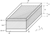
- the chip connection portion may have a main material portion.
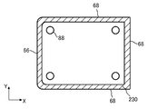
- the chip connection portion may have an obstruction portion that is formed of a material having a lower solder wettability than the main material portion and is exposed and arranged on the tip surface.
- a fifth aspect of the present invention provides a method for manufacturing a semiconductor module.
- the semiconductor module includes an insulated circuit board having a circuit pattern formed on one surface, a semiconductor chip mounted on the insulated circuit board, and a wiring unit for electrically connecting the semiconductor chip and the circuit pattern. May have a chip connection that connects to the semiconductor chip.
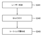
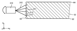
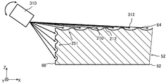
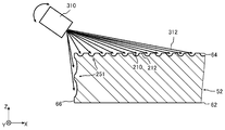
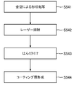
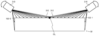
- the surface of the chip connection portion may be irradiated with a laser to form a plurality of recesses and a flat surface portion arranged between the two recesses.
- a sixth aspect of the present invention provides a method for manufacturing a semiconductor module.
- the semiconductor module includes an insulated circuit board having a circuit pattern formed on one surface, a semiconductor chip mounted on the insulated circuit board, and a wiring unit for electrically connecting the semiconductor chip and the circuit pattern. May have a chip connection that connects to the semiconductor chip.
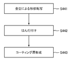
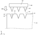
- the shape may be transferred to the upper surface of the chip connection portion by a mold to form a plurality of recesses and a flat surface portion arranged between the two recesses.
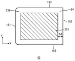
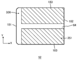
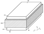
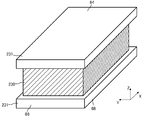
- FIG. 2 is a cross-sectional view taken along the line AA of FIG. It is an enlarged view of the lead frame 50 of FIG. It is an enlarged view of the vicinity of a circuit pattern connection part 56. It is an enlarged view of the vicinity of the tip surface 66 of FIG. It is a figure which shows the relationship between the development area ratio in a lead frame 50, and the adhesion strength. It is a perspective view which shows the other structural example of a lead frame 50. It is a figure which shows the lower surface 62 of the chip connection part 52 of FIG.
- FIG. 39 It is a figure which shows another example of a lead frame 50. It is a figure which shows the arrangement example of the obstruction part 230 on the lower surface 62 of the chip connection part 52. It is an enlarged schematic diagram of the chip connection part 52 of FIGS. 39 and 40. It is a figure which shows the other arrangement example of the obstruction part 230 on the lower surface 62 of the chip connection part 52. It is a figure which shows the other arrangement example of the main material part 231 and the obstruction part 230 in a chip connection part 52. It is a figure which shows the other arrangement example of the main material part 231 and the obstruction part 230 in a chip connection part 52. It is a figure which shows the other arrangement example of the main material part 231 and the obstruction part 230 in a chip connection part 52. It is a figure which shows the other arrangement example of the main material part 231 and the obstruction part 230 in a chip connection part 52.
- one side in the direction parallel to the depth direction of the semiconductor chip is referred to as "upper”, and the other side is referred to as “lower”.
- the upper surface is referred to as the upper surface and the other surface is referred to as the lower surface.
- the “up” and “down” directions are not limited to the direction of gravity or the direction when the semiconductor module is mounted.
- orthogonal coordinate axes of X-axis, Y-axis, and Z-axis Orthogonal axes only specify the relative positions of the components and do not limit a particular direction.
- the Z axis does not limit the height direction with respect to the ground.
- the + Z-axis direction and the ⁇ Z-axis direction are opposite to each other.
- positive or negative is not described and is described as the Z-axis direction, it means the direction parallel to the + Z-axis and the -Z-axis.
- the orthogonal axes parallel to the upper surface and the lower surface of the semiconductor chip are defined as the X axis and the Y axis.
- the axis perpendicular to the upper surface and the lower surface of the semiconductor substrate is defined as the Z axis.
- the direction of the Z axis may be referred to as a depth direction.
- the direction parallel to the upper surface and the lower surface of the semiconductor substrate including the X-axis and the Y-axis may be referred to as a horizontal direction.
- error When referred to as “same” or “equal” in the present specification, it may include a case where there is an error due to manufacturing variation or the like.
- the error is, for example, within 10%.
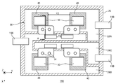
- FIG. 1 is a diagram showing an example of a semiconductor module 100 according to an embodiment of the present invention.
- the semiconductor module 100 may function as a power conversion device such as an inverter.
- the semiconductor module 100 includes one or more insulated circuit boards 160.
- the orthogonal axes on the plane on which one or more insulating circuit boards 160 are provided are the X-axis and the Y-axis, and the axes perpendicular to the XY plane are the Z-axis.
- FIG. 1 shows an example of arrangement of each member on the XY plane.
- the semiconductor module 100 of this example includes three insulated circuit boards 160, each of which constitutes an arm of a U layer, a V layer, and a W layer.
- One or more semiconductor chips 40 are mounted on the insulating circuit board 160.
- the semiconductor chip 40 is protected by a resin package 14 such as a resin case 10 surrounding the insulating circuit board 160 and a sealing resin 12 filled in the resin case 10.
- the semiconductor chip 40 may include an isolated gate type bipolar transistor (IGBT), a diode such as an FWD (Free Wheel Diode), an RC (Reverse Control) -IGBT combining these, a MOS transistor, and the like.
- IGBT isolated gate type bipolar transistor
- FWD Free Wheel Diode
- RC Reverse Control
- the resin case 10 is provided so as to surround the space 94 that accommodates the insulating circuit board 160.
- One or more terminals 86 may be provided so as to be exposed from the resin case 10.
- the terminal 86 may be electrically connected to the insulating circuit board 160 via the terminal connection portion 198.
- the resin case 10 may be provided with a through hole 84 into which a fastening member such as a screw for fixing a cooling device or the like is inserted.
- the resin case 10 is molded from a resin such as a thermosetting resin that can be formed by injection molding or an ultraviolet curable resin that can be formed by UV molding.
- the resin contains, for example, one or more polymer materials selected from polyphenylene sulfide (PPS) resin, polybutylene terephthalate (PBT) resin, polyamide (PA) resin, acrylonitrile butadiene styrene (ABS) resin, acrylic resin and the like. It's fine.
- the sealing resin 12 is provided inside the resin case 10.
- the sealing resin 12 is, for example, an epoxy resin or a silicone gel, but is not limited thereto.
- the sealing resin 12 can protect the insulating circuit board 160.
- FIG. 2 is a diagram showing an example of the insulated circuit board 160.
- the insulating circuit board 160 constituting the arm of one phase is exemplified as a representative, but the insulating circuit board 160 of the other phase also has the same configuration.
- the circuit pattern 26 is provided on one surface of the insulating substrate 20, and the heat sink 22 (see FIG. 3) is provided on the other surface.
- a copper plate or an aluminum plate, or a plate obtained by plating these materials is directly bonded to an insulating substrate 20 such as silicon nitride ceramics or aluminum nitride ceramics, or bonded via a brazing material layer. It may be configured by.
- the semiconductor chip 40 of this example is bonded to a circuit pattern 26 provided on the upper surface of the insulating substrate 20 via a bonding layer 30 (see FIG. 3) such as solder. Further, the upper surface of the semiconductor chip 40 is connected to the wiring portion via a bonding layer 32 (see FIG. 3) such as solder.
- the wiring portion of this example is a lead frame 50.
- the lead frame 50 connects the semiconductor chip 40 to the circuit pattern 26 via a bonding layer 34 (see FIG. 3) such as solder.
- the lead frame 50 is a member made of a metal material such as copper or aluminum. At least a part of the surface of the lead frame 50 may be plated with nickel or the like.
- the lead frame 50 may be coated with a resin or the like.
- the lead frame 50 may have a plate-shaped portion.
- the plate shape refers to a shape in which the area of two main surfaces arranged facing each other is larger than the area of the other surface.
- the lead frame 50 may have at least a plate-like portion connected to the semiconductor chip 40.
- the lead frame 50 may be formed by bending one metal plate.
- the circuit pattern 26 transmits a signal or electric power by being electrically connected to the semiconductor chip 40 or the lead frame 50.
- the circuit pattern 26 may be configured to include a plurality of island-shaped regions 26A, 26B, 26C. Further, a plurality of semiconductor chips 40 may be arranged in one island-shaped region of the circuit pattern 26. In the example of FIG. 2, a plurality of semiconductor chips 40 are arranged in each of the island-shaped regions 26A and 26B. Further, a plurality of semiconductor chips 40 arranged in one island-shaped region may be connected to the same island-shaped region by a lead frame 50. In the example of FIG.
- a plurality of semiconductor chips 40 arranged in the island-shaped region 26A are connected in parallel to the same island-shaped region 26B by two read frames 50 arranged in the Y-axis direction. Further, a plurality of semiconductor chips 40 arranged in the island-shaped region 26B are connected in parallel to the same island-shaped region 26C by two lead frames 50 arranged in the Y-axis direction.
- the distance Y1 in the Y-axis direction of the connecting portion connected to the same island-shaped region 26B or 26C may be smaller than the distance Y2 in the Y-axis direction of the two semiconductor chips 40. This makes it possible to reduce the difference in the path length of the current passing through the two semiconductor chips 40 arranged apart from each other.
- the semiconductor chip 40 of this example is a vertical chip in which electrodes (for example, an emitter electrode and a collector electrode) are formed on the upper surface and the lower surface.
- the semiconductor chip 40 is connected to the circuit pattern 26 by an electrode formed on the lower surface, and is connected to the lead frame 50 by an electrode formed on the upper surface.
- the semiconductor chip 40 is not limited to the vertical chip.
- the semiconductor chip 40 may have an electrode connected to the circuit pattern 26 on the upper surface. In this case, the circuit pattern 26 and the electrode may be connected by a wire or the like.
- the terminal connection portion 198 connects the circuit pattern 26 and the terminal 86 shown in FIG.
- the terminal connection portion 198 may be a plate or rod-shaped member made of metal, or may be a wire-shaped member. As a result, the semiconductor chip 40 and the terminal 86 are electrically connected.
- FIG. 3 is a sectional view taken along the line AA of FIG. FIG. 3 shows an arrangement example of each member when each member is projected onto the XZ plane.
- the semiconductor module 100 includes an insulating substrate 20, a heat sink 22, a bonding layer 24, a cooling unit 16, a circuit pattern 26, a bonding layer 30, 32, 34, a semiconductor chip 40, a lead frame 50, and a sealing resin 12. Be prepared.
- the heat radiating plate 22 may cover at least a part or the whole of the lower surface of the insulating substrate 20.
- the joining layer 24 joins the heat sink 22 to the cooling unit 16.
- the bonding layer 24 is solder or the like.
- the cooling unit 16 contains a refrigerant such as water inside. The cooling unit 16 cools the semiconductor chip 40 via the heat sink 22 and the like.
- the circuit pattern 26 is arranged on the upper surface of the insulating substrate 20.
- the circuit pattern 26 may be formed of the same material as the heat sink 22 such as copper, or may be formed of a different material.
- the semiconductor chip 40 of this example is connected to the upper surfaces of the island-shaped regions 26A and 26B of the circuit pattern 26 by a bonding layer 30.
- the bonding layer 30 joins the semiconductor chip 40 with a conductive material such as solder.
- the lead frame 50 of this example connects the semiconductor chip 40 and the island-shaped regions 26B and 26C of the circuit pattern 26.
- the lead frame 50 of this example has a chip connection portion 52, a circuit pattern connection portion 56, and a cross-linking portion 54.
- the chip connecting portion 52 is a portion bonded to the upper surface of the semiconductor chip 40 by the bonding layer 32.
- the circuit pattern connecting portion 56 is a portion connected to the upper surface of the island-shaped regions 26B and 26C of the circuit pattern 26 by the bonding layer 34.
- the chip connection portion 52 and the circuit pattern connection portion 56 may be plate-shaped portions substantially parallel to the XY plane. In addition, almost parallel means, for example, a state where the angle is 10 degrees or less.
- the area of the chip connecting portion 52 is configured to be larger than the area of the circuit pattern connecting portion 56.
- the area of the chip connecting portion 52 and the area of the circuit pattern connecting portion 56 may be, for example, the area of the upper surface of the plate-shaped portion connected to the island-shaped regions 26B and 26C of the semiconductor chip 40 and the circuit pattern 26.
- the bridging portion 54 connects the chip connecting portion 52 and the circuit pattern connecting portion 56.
- the cross-linking portion 54 is arranged away from the conductive member such as the circuit pattern 26.
- the cross-linking portion 54 of this example is arranged above the circuit pattern 26 or the like, and is provided so as to straddle the circuit pattern 26 or the like from the chip connection portion 52 to the circuit pattern connection portion 56.
- the cross-linking portion 54 may have a cross-linking surface 54A (see FIG. 4) which is a plate-shaped member substantially parallel to the XY surface. Further, the cross-linking portion 54 may have a leg portion 54B (see FIG. 4) that connects the chip connecting portion 52 and the cross-linking surface 54A. Further, the cross-linking portion 54 may have a leg portion 54C (see FIG. 4) that connects the cross-linking surface 54A and the circuit pattern connection portion 56.
- the leg portion 54B and the leg portion 54C may be plate-shaped portions that are not parallel to the XY plane. For example, the leg portion 54B and the leg portion 54C may be formed so that the angle with respect to the XY surface is 45 degrees or more.
- the leg portion 54B and the leg portion 54C of this example include a portion perpendicular to the XY plane.
- the cross-linked portion 54 is provided with an opening 74 (see FIG. 2) for injecting the sealing resin 12 below the cross-linked portion 54.
- the cross-linking portion 54 of this example is provided with a plurality of openings 74 inside the cross-linking portion 54 on the XY plane and near the center of the cross-linking portion 54 in the X-axis direction.
- the plurality of openings 74 may be provided in a region not near the center of the bridge portion 54 in the X-axis direction.
- the opening 74 is not limited to the cross-linking portion 54, and may be provided in other portions of the lead frame 50 such as the chip connecting portion 52 and the circuit pattern connecting portion 56. As a result, the sealing resin 12 can be reliably spread above and below the lead frame 50.
- the sealing resin 12 is provided inside the resin case 10.
- the sealing resin 12 may be filled in the space 94 of the resin case 10 so that the semiconductor chip 40, the lead frame 50, and the circuit pattern 26 are not exposed.
- the semiconductor chip 40 serves as a heat source, and the chip connection portion 52 of the wiring connected to the semiconductor chip 40 repeatedly expands and contracts due to a temperature change. Since the sealing resin 12 around the chip connecting portion 52 also repeats expansion and contraction due to temperature changes, it is desirable to match the linear expansion coefficient of the wiring and the sealing resin 12. However, even if the coefficients of linear expansion are matched, the tip surface 66 of the chip connecting portion 52 is likely to be peeled off due to the difference in temperature distribution and shrinkage rate. Further, since the semiconductor chip 40 is a heat generation source, the chip connection portion 52 has a higher risk of being repeatedly exposed to thermal stress than the circuit pattern connection portion 56. In addition, in this example, the area of the chip connecting portion 52 is configured to be larger than the area of the circuit pattern connecting portion 56. Also in this respect, the chip connection 52 has a higher risk when exposed to thermal stress than the circuit pattern connection 56.
- the leg portion 54B (see FIG. 4) is restrained by the sealing resin 12, and is difficult to move. Since the leg portion 54B acts as an axis, the portion of the chip connecting portion 52 that can be relatively fragile due to stress is considered to be the tip surface 66 (see FIG. 4). In other words, in the semiconductor module 100, the portion that can be relatively fragile due to stress is considered to be the tip surface 66.
- the semiconductor module 100 of this example may have the configuration described below.
- FIG. 4 is an enlarged view of the lead frame 50 of FIG.
- the lead frame 50 has a rough surface region 51 in at least a part of the surface.
- the surface provided with the rough surface region 51 is shown by a broken line.
- the rough surface region 51 is a region having a developed area ratio (Sdr) of 0.2 or more.
- the developed area ratio represents the rate of increase in the surface area of the defined area with respect to the projected area when projected onto a predetermined plane in the predetermined defined area.
- a perfectly flat definition area has a surface area equal to the projected area, so the unfolded area ratio is zero.
- the projected area does not change, but the surface area increases, so that the developed area ratio becomes large.
- the developed area ratio of the rough surface region 51 may be 0.3 or more, and may be 0.4 or more.
- the arithmetic mean height (Sa) of the rough surface region 51 may be 10 ⁇ m or less.
- the arithmetic mean height is the average value of the height or depth of each unevenness of the rough surface region 51 with respect to the surface obtained by averaging the height of the rough surface region 51. That is, the rough surface region 51 is a region in which the developed area ratio is increased due to fine irregularities.
- the maximum height (Sz) of the rough surface region 51 may be 100 ⁇ m or less. The maximum height represents the distance from the highest point to the lowest point of each unevenness of the rough surface region 51.
- the expanded area ratio (Sdr), arithmetic mean height (Sa), and maximum height (Sz) in the present embodiment may follow the definitions of ISO 25178, which is an international standard.
- the following are examples of the measurement environment for each parameter. However, as a matter of course, it is possible to use the values measured not only in this measurement environment but also in the same measurement environment.
- Measuring instrument KEYENCE VK-X1100 Controller part: Keyence VK-X1000 Objective lens: Apo x 50x Cutoff: Gaussian S Filter: None L Filter: None F-Operation: None
- the rough surface region 51 can be formed by irradiating the lead frame 50 with a laser. In this case, the rough surface region 51 local to the lead frame 50 can be easily formed. Further, the rough surface region 51 may be formed by injecting a predetermined particle onto a part or the whole of the lead frame 50, or may be formed by immersing a part or the whole of the lead frame 50 in a predetermined solution. , May be formed by other methods.
- the rough surface region 51 may be provided in the chip connection portion 52.
- the semiconductor chip 40 serves as a heat source. Therefore, stress is likely to be applied to the chip connection portion 52 connected to the semiconductor chip 40. When stress is applied to the lead frame 50, the lead frame 50 and the sealing resin 12 are easily peeled off.
- the contact area between the lead frame 50 and the sealing resin 12 can be increased, so that the peeling of the sealing resin 12 can be suppressed. Further, by locally providing the rough surface region 51, it becomes easy to reduce the manufacturing cost of the lead frame 50.
- the surface farthest from the cross-linked portion 54 is referred to as the tip surface 66.
- the surface facing the semiconductor chip 40 that is, the surface joined to the semiconductor chip 40 is the lower surface 62
- the surface opposite to the lower surface 62 is the upper surface 64
- the lower surface 62 and the upper surface 64 are planes substantially parallel to the XY plane.
- the front end surface 66 and the side surface 68 are surfaces that are not parallel to the XY surface.
- the tip surface 66 and the side surface 68 may be substantially perpendicular to the XY surface.
- the rough surface region 51 is preferably provided on at least a part of the tip surface 66.
- the tip surface 66 is a portion that can be relatively fragile, and peeling from the sealing resin 12 is likely to occur.
- the rough surface region 51 may be provided over half or more of the tip surface 66, or may be provided over the entire tip surface 66.
- the portion in contact with the lower surface 62 is a portion that may come into contact with the joint layer 32 such as solder, and the joint layer 32 such as solder may cause a starting point of resin peeling.
- the joint layer 32 such as solder may cause a starting point of resin peeling.
- the rough surface region 51 may be provided on at least a part of the upper surface 64. By providing the rough surface region 51 on the upper surface 64, peeling between the lead frame 50 and the sealing resin 12 can be further suppressed.
- the rough surface region 51 may be provided over half or more of the upper surface 64, or may be provided over the entire upper surface 64. When the rough surface region 51 is provided on a part of the upper surface 64, it is preferable to provide the rough surface region 51 on the portion of the upper surface 64 in contact with the tip surface 66.
- the rough surface region 51 may be provided on at least a part of the side surface 68. By providing the rough surface region 51 on the side surface 68, peeling between the lead frame 50 and the sealing resin 12 can be further suppressed.
- the rough surface region 51 may be provided over half or more of the side surface 68, or may be provided over the entire side surface 68. When the rough surface region 51 is provided on a part of the side surface 68, the rough surface region 51 may be provided on the portion of the side surface 68 in contact with the tip surface 66.
- a rough surface region 51 may be provided on the side surface 68 in contact with the third side 83, which will be described later. Further, a rough surface region 51 may be provided on a portion of the side surface 68 in contact with the lower surface 62.
- the rough surface region 51 does not have to be provided on the lower surface 62. This is because the lower surface 62 is connected to the semiconductor chip 40 via the bonding layer 32.
- the lower surface 62 of the chip connecting portion 52 is provided with a plurality of protruding portions 88 protruding toward the insulating circuit board 160, that is, the semiconductor chip 40.
- a plurality of protrusions 88 projecting toward the island-shaped regions 26B and 26C of the insulating circuit board 160, that is, the circuit pattern 26 may be provided on the lower surface of the circuit pattern connection portion 56.
- the length of the protrusion 88 in the X-axis direction may be 1/4 or less, or 1/8 or less, the length of the chip connection portion 52 or the circuit pattern connection portion 56 in the X-axis direction.
- the length of the protrusion 88 in the Y-axis direction may be 1/4 or less, or 1/8 or less, of the length of the chip connection portion 52 or the circuit pattern connection portion 56 in the Y-axis direction. ..
- the lower surface 62 of the chip connection portion 52 or the circuit pattern connection portion 56 is arranged parallel to the upper surface of the island-shaped regions 26B and 26C of the semiconductor chip 40 or the circuit pattern 26, and the bonding layer 32 such as solder is provided. Can be formed well.
- the protrusion 88 is omitted in FIGS. 3, 5, and 6.
- FIG. 5 is an enlarged view of the vicinity of the circuit pattern connection portion 56.
- the island-shaped regions 26B and 26C of the circuit pattern 26 are joined to the circuit pattern connecting portion 56 of the lead frame 50 by the joining layer 34.
- the expanded area ratio in the rough surface region 51 of the chip connecting portion 52 may be larger than the expanded area ratio in the circuit pattern 26.
- the developed area ratio of the circuit pattern 26 may use the value of the region 39 in contact with the sealing resin 12.
- the developed area ratio of the circuit pattern 26 is 0.08 or less.
- the spread area ratio of the island-shaped regions 26B of the circuit pattern 26 has been illustrated and described, but the spread area ratios of the island-shaped regions 26A and 26C of the circuit pattern 26 may be the same.
- the circuit pattern connection portion 56 may or may not be provided with a rough surface region 51.
- the circuit pattern connection portion 56 of this example is not provided with a rough surface region 51. That is, the expanded area ratio of each surface of the circuit pattern connecting portion 56 of this example is smaller than the expanded area ratio of the rough surface region 51 provided in the chip connecting portion 52.
- the expanded area ratio on each surface of the circuit pattern connecting portion 56 may be smaller than 0.2.
- the expanded area ratio of each surface of the circuit pattern connecting portion 56 may be 0.08 or less.
- the rough surface region 51 may be provided on the entire surface of the lead frame 50. This may facilitate the processing of the lead frame 50.
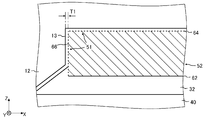
- FIG. 6 is an enlarged view of the vicinity of the tip surface 66 of FIG.
- the coating layer 13 is a thermoplastic high heat resistant film formed of a resin.
- the coating layer 13 may be formed by spraying the members to each member by spraying or the like after joining the members with solder or the like and before filling the sealing resin 12.
- the coating layer 13 may be formed for each member before joining the members with solder or the like.
- the coating layer 13 may be applied using a high-performance controlled dispense device (liquid fixed-quantity discharge device).
- the coating layer 13 may be formed of a resin having higher heat resistance than the sealing resin 12.
- the coating layer 13 may be formed of a resin having higher flexibility than the sealing resin 12.
- the coating layer 13 is formed of, for example, a polyamide-based resin, a polyamide-imide-based resin, or a polyimide-based resin, but the material is not limited thereto.
- the coating layer 13 may be provided on a surface of the surface of the lead frame 50 other than the surface facing the semiconductor chip 40, or may be provided on the entire surface.
- the coating layer 13 preferably covers at least the rough surface region 51.
- the coating layer 13 may be applied so as to cover the tip surface 66, the upper surface 64, and the side surface 68.
- the film thickness T1 of the coating layer 13 is, for example, 1 ⁇ m or more and 100 ⁇ m or less.
- the film thickness T1 of the coating layer 13 may be preferably 2 ⁇ m or more, more preferably 3 ⁇ m or more.
- the film thickness T1 of the coating layer 13 may be an average thickness in a predetermined range.
- the surface of the coating layer 13 covering the rough surface region 51 may have irregularities corresponding to the irregularities of the rough surface region 51, and may be flatter than the rough surface region 51.
- peeling of the sealing resin 12 can be further suppressed.
- the fact that the coating layer 13 is provided with irregularities corresponding to the irregularities of the rough surface region 51 means that the concave portions of the rough surface region 51 and the concave portions of the coating layer 13 overlap when viewed from a direction perpendicular to the rough surface region 51. It means that it is arranged at a position, and the convex portion of the rough surface region 51 and the convex portion of the coating layer 13 are arranged at the overlapping position.
- the coating layer 13 and the sealing resin 12 may be bonded by a chemical bond.
- the chemical, mechanical, and physical bonds between the coating layer 13 and the sealing resin 12 can ensure the strength between them.
- solder or the like of the bonding layer 32 may enter between the sealing resin 12 and the lead frame 50.
- solder or the like may crawl up on the tip surface 66.
- the adhesion between the bonding layer 32 such as solder and the resin is relatively poor.
- the possibility that the coating layer 13) is peeled off from the bonding layer 32 increases.
- the adhesion between the resin and the lead frame 50 is improved by providing the rough surface region 51, even if the resin is peeled from the bonding layer 32, the resin peeling progresses. Therefore, it is possible to prevent the resin from peeling off from the lead frame 50 as well.
- the chip connecting portion 52 is a place where stress is easily applied as described above, so to speak, the chip connecting portion 52 is a portion that affects the durability of the resin peeling of the semiconductor module 100.
- the expanded area ratio of the chip connecting portion 52 in the rough surface region 51 is made larger than the expanded area ratio of the circuit pattern connecting portion 56. This makes it possible to increase the durability of the chip connection portion 52, which has been a bottleneck.
- increasing the unfolded area ratio of the chip connecting portion 52, which can be relatively fragile, to be larger than the unfolded area ratio of the circuit pattern connecting portion 56 means that the circuit pattern connecting portion 56 does not require processing or the like. It is possible to suppress the increase in cost without increasing the number of processes more than necessary.
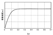
- FIG. 7 is a diagram showing the relationship between the unfolded area ratio in the lead frame 50 and the adhesion strength.
- the force for pulling the resin (here, the coating layer 13) and the lead frame 50 are increased, the magnitude of the force when the resin is peeled off is defined as the adhesion strength.
- the expansion area ratio in each region of the lead frame 50 was changed, and the adhesion strength in the region was measured.
- the arithmetic mean height (Sa) of the rough surface region 51 is set to 10 ⁇ m or less
- the maximum height (Sz) of the rough surface region 51 is set to 100 ⁇ m or less.
- the experiment was conducted under conditions that were not extremely high. By setting the arithmetic mean height (Sa) and the maximum height (Sz) of the rough surface region 51 within the predetermined ranges in this way, it is possible to avoid the possibility of affecting the performance of other products.
- the lead frame 50 has a structure that suppresses the creeping up of solder or the like on the tip surface 66.
- a structure for suppressing the creeping up of the solder or the like will be described.
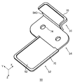
- FIG. 8 is a perspective view showing another structural example of the lead frame 50.
- the lower surface 62 of the chip connecting portion 52 facing the semiconductor chip 40 is provided with a step 70.
- the lower surface of the circuit pattern connecting portion 56 may be provided with a step 70 similar to that of the chip connecting portion 52.
- the protrusion portion 88 is not provided on the chip connection portion 52 and the circuit pattern connection portion 56.
- FIG. 9 is a diagram showing a lower surface 62 of the chip connection portion 52 of FIG.
- the side farthest from the bridge portion 54 is referred to as the first side 81.
- the lower surface 62 is a substantially rectangular shape having two sets of two parallel sides, but may have other shapes.
- the side of the lower surface 62 may be a straight line.
- the first side 81 is connected to the tip surface 66.
- the second side 82 the side closest to the bridge portion 54
- the third side 83 is connected to the side surface 68.
- the first side 81 and the third side 83 may be connected by a curve.
- the length of the first side 81 be L1.
- the first side 81 of this example is a line extending in the Y-axis direction.
- the length L1 is the distance between the two third sides 83 in the Y-axis direction.
- the lower surface 62 is provided with a step 70 along the first side 81 over a length of more than half the length of the first side 81.
- the fact that the step 70 is along a predetermined side means that the angle between the stretching direction of the step 70 and the stretching direction of the side is 15 degrees or less, or 5 degrees or less. You may point to the state of 0 degrees.
- the step 70 may be in contact with the first side 81. Further, the distance between the step 70 and the first side 81 may be less than half of the distance between the first side 81 and the second side 82 in the X-axis direction, and may be 1/4 or less. It may be 1/10 or less. The step 70 may be 1 ⁇ 2 or more of the length of the first side 81 in the Y-axis direction, and may be 3/4 or more. The step 70 may be provided over the entire first side 81. As a result, it is possible to prevent the bonding layer 32 such as solder from creeping up on the tip surface 66 where stress is most likely to be applied.
- the step 70 may be provided along the third side 83.
- the lower surface 62 may be provided with a step 70 along the third side 83 over a length of half or more of the third side 83.
- the step 70 may be in contact with the third side 83.
- the distance between the step 70 and the third side 83 may be half or less of the length L1, may be 1/4 or less, and may be 1/10 or less.
- the step 70 may be provided over a length of 1 ⁇ 2 or more or 3/4 or more of the length of the third side 83 in the X-axis direction.
- the step 70 may be provided over the entire third side 83. As a result, it is possible to prevent the bonding layer 32 such as solder from creeping up on the side surface 68.
- the second side 82 may or may not be provided with a step 70.
- the step 70 is not provided on the entire second side 82.
- the step 70 may be provided along a side other than the second side 82 among the sides of the lower surface 62.
- the above-mentioned step 70 may be inclined. That is, an inclination of 1 ⁇ 2 or more or 3/4 or more of the length of the first side 81 in the Y-axis direction along the first side 81 may be provided. Further, an inclination of 1/2 or more or 3/4 or more of the length of the third side 83 in the X-axis direction along the third side 83 may be provided.
- the step 70 includes at least one of a protrusion and a groove.
- the protruding portion protrudes from the lower surface 62 toward the semiconductor chip 40, as in the example shown in FIG.
- the groove portion is recessed in a direction away from the semiconductor chip 40 from the lower surface 62.
- the side wall of the step 70 may be perpendicular to the lower surface 62 and may have an angled tapered shape.
- FIG. 10 is a diagram showing a BB cross section in FIG.
- the BB cross section is an XZ cross section.
- the step 70 in this example is a protruding portion, it may be a groove portion.
- the step 70 is arranged along the tip surface 66.
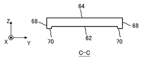
- FIG. 11 is a diagram showing a CC cross section in FIG.
- the CC cross section is a YZ cross section.
- the step 70 is arranged along the side surface 68 connected to the tip surface 66.
- FIG. 12 is an enlarged view of the vicinity of the tip surface 66 when the lead frame 50 of FIG. 8 is applied.
- the step 70 in this example is a protruding portion arranged in contact with the tip surface 66.
- the height (or depth) of the step 70 with respect to the lower surface 62 in the Z-axis direction may be half or less of the thickness of the chip connecting portion 52 in the Z-axis direction, or may be 1/4 or less.
- the step 70 by providing the step 70, it becomes easy to define the position of the end portion of the joint layer 32 such as solder. That is, the position of the end portion of the joining layer 32 tends to coincide with the position of the end portion of the step 70. As a result, it is possible to prevent the joining layer 32 from crawling up on the tip surface 66 and the like.
- the lead frame 50 having the step 70 may or may not be provided with the rough surface region 51. Further, the lead frame 50 may or may not be covered with the coating layer 13.
- the rough surface region 51 is provided in at least a part of the lower surface 62 of the lead frame 50 where the step 70 is provided.
- a rough surface region 51 may be provided on the entire step 70.
- peeling of the sealing resin 12 can be further suppressed.
- at least a part of the lower surface 62 where the step 70 is provided may be covered with the coating layer 13.
- FIG. 13 is a diagram showing another example of the lower surface 62 of the chip connecting portion 52.
- the step 70 in this example is a groove portion arranged in contact with the tip surface 66.
- the other composition of the step 70 is the same as the step 70 described with reference to FIGS. 9 to 12.
- the step 70 is provided along the first side 81 and the third side 83. Specifically, the step 70 is provided in contact with the first side 81 and the third side 83.
- the step 70 may be in contact with each side or may be separated from each other.
- a plurality of protrusions 88 are provided on the lower surface 62 of the chip connection portion 52.
- the length of the protrusion 88 in the X-axis and Y-axis directions is shorter than that of the step 70.
- the length of the protrusion 88 in the X-axis direction may be 1/4 or less, or 1/8 or less, the length of the chip connection portion 52 in the X-axis direction.
- the length of the protrusion 88 in the Y-axis direction may be 1/4 or less, or 1/8 or less, of the length of the chip connection portion 52 in the Y-axis direction.
- the height of the protrusion 88 in the Z-axis direction is lower than that of the step 70.
- FIG. 14 is a diagram showing a DD cross section in FIG.
- the DD cross section is an XZ cross section.
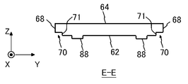
- FIG. 15 is a diagram showing a cross section of EE in FIG.
- the EE cross section is a YZ cross section.
- the step 70 is arranged along the tip surface 66 and the side surface 68 connected to the tip surface 66.
- a fillet (hem portion) of the bonding layer 32 such as solder is formed on the receding surface 71 of the step 70 which is a groove portion, and it is possible to prevent the solder or the like from creeping up on the tip surface 66 and the side surface 68.
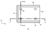
- FIG. 16 is a diagram showing another example of the lower surface 62 of the chip connecting portion 52.
- the step 70 in this example is a groove portion arranged away from the front end surface 66 and the side surface 68 connected to the front end surface 66.
- the other composition of the step 70 is the same as the step 70 described with reference to FIGS. 9 to 15.
- the step 70 is provided along the first side 81 and the third side 83.
- the step 70 may be in contact with each side or may be separated from each other.
- the step 70, which is a groove portion is provided apart from the first side 81 and the third side 83.
- a plurality of protrusions 88 are provided on the lower surface 62 of the chip connection portion 52.
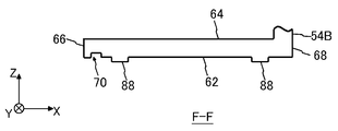
- FIG. 17 is a diagram showing a cross section of FF in FIG.
- the FF cross section is an XZ cross section.
- FIG. 18 is a diagram showing a GG cross section in FIG.
- the GG cross section is a YZ cross section.
- the step 70 is arranged along the tip surface 66 and the side surface 68 connected to the tip surface 66.
- the step 70 is arranged between the protrusion 88 and the tip surface 66 or the side surface 68 connecting the protrusion 88 and the tip surface 66.
- a bonding layer 32 such as solder is housed in a step 70 which is a groove portion, and a fillet such as solder is formed from this step, so that it is possible to prevent the solder or the like from creeping up on the tip surface 66 and the side surface 68.
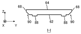
- FIG. 19 is a diagram showing another example of the lower surface 62 of the chip connection portion 52.
- the lower surface 62 of the chip connecting portion 52 is provided with an inclination 90.
- the inclination 90 is inclined at a predetermined angle so as to move away from the semiconductor chip 40 toward the outside of the lower surface 62.
- Other structures are the same as the chip connection portion 52 described above.
- the height of the protrusion 88 in the Z-axis direction may be lower than the inclination 90.
- FIG. 20 is a diagram showing a cross section of HH in FIG.
- the HH cross section is an XZ cross section.
- the inclination 90 is arranged in contact with the tip surface 66. Specifically, the inclination 90 is provided from the lower surface 62 to the tip surface 66. That is, the inclination 90 is formed by chamfering the corner portion of the lower surface 62, that is, the corner connecting the lower surface 62 and the tip surface 66.
- the angle between the inclination 90 and the lower surface 62 may be 20 degrees or more and 70 degrees or less.
- the fillet of the joining layer 32 is stabilized in a shape corresponding to the angle of the slope 90. Therefore, the shape of the fillet of the joining layer 32 can be stabilized. Therefore, it is possible to suppress the peeling of the resin due to the variation in the fillet shape of the bonding layer 32. Further, since the inclination 90 can be formed by chamfering the corners, it is easy to process.
- FIG. 21 is a diagram showing an I-I cross section in FIG.
- the I-I cross section is a YZ cross section.
- the inclination 90 is arranged in contact with the side surface 68 connected to the tip surface 66. Similar to the example of FIG. 20, the slope 90 has an angle with respect to the lower surface 62.
- the inclination 90 is provided from the lower surface 62 to the side surface 68 connected to the tip surface 66. That is, the inclination 90 is formed by chamfering the corner portion of the lower surface 62, that is, the corner of the lower surface 62 and the side surface 68 connected to the tip surface 66.
- the angle between the inclination 90 and the lower surface 62 may be 20 degrees or more and 70 degrees or less.
- the fillet shape of the joining layer 32 can be stabilized.
- the inclination 90 is inclined at a predetermined angle so as to move away from the semiconductor chip 40 toward the outside of the lower surface 62, but is formed so as to approach the semiconductor chip 40 toward the outside of the lower surface 62. You may.
- FIG. 22 is a diagram showing a chip connection portion 152 according to a reference example.
- the chip connecting portion 152 has the same structure as the chip connecting portion 52 except that the rough surface region 51 is not provided.
- the tip surface 66 or the side surface 68 of the chip connection portion 152 has solder wettability. Therefore, the solder 32 may crawl up along the tip surface 66 or the side surface 68.
- the coating layer 13 is formed after the solder 32 crawls up along the tip surface 66 or the side surface 68, the solder 32 is interposed between the tip surface 66 or the side surface 68 of the chip connecting portion 152 and the coating layer 13. ..
- the bonding force between the coating layer 13 and the solder 32 is relatively weak. Therefore, the coating layer 13 may be peeled off due to thermal stress or the like.
- the area in contact between the chip connecting portion 52 and the tip surface 66 and the like becomes smaller, so that the coating layer 13 is more easily peeled off. Further, if the peeling of the coating layer 13 progresses, cracks may occur in the sealing resin 12.
- FIG. 23 is an enlarged view of the vicinity of the apex 201 of the chip connection portion 152. As described above, when the solder 32 crawls up to the vicinity of the apex 201, the coating layer 13 may be peeled off in the vicinity of the apex 201. FIG. 23 shows the space 202 created by the peeling of the coating layer 13.
- the adhesion strength between the solder 32 and the coating layer 13 is insufficient, so that the solder 32 easily moves due to thermal stress, and cracks 203 may occur in the coating layer 13.
- the sealing resin 12 may also have a crack 204.
- the crack 204 occurs, the lead frame 50, the semiconductor chip 40, and the like cannot be sufficiently protected.
- FIG. 24 is a diagram showing another example of the lead frame 50.
- the lead frame 50 of this example is provided with an inhibition region 251 on the surface of the chip connecting portion 52 in place of the rough surface region 51 described in FIGS. 1 to 21.
- the structure other than the inhibition region 251 may be the same as any of the forms described in FIGS. 1 to 21.
- the inhibition region 251 inhibits the wetting and spreading of the solder. That is, the inhibition region 251 is a region having a lower solder wettability than the surface of the lead frame 50 in which the inhibition region 251 is not provided.
- the solder wettability may be indicated by the size of the area where the region where the solder spreads is projected onto a plane when a predetermined mass of solder is placed on the target surface and heated under predetermined conditions. Further, the solder wettability may be indicated by a height at which the solder crawls up the target surface when a predetermined mass of solder is arranged at the lower end of the vertically arranged target surface and heated under predetermined conditions.
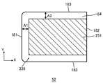
- the inhibition region 251 is provided at least on the tip surface 66 of the chip connection portion 52.
- the inhibition region 251 may be provided in a part of the tip surface 66, or may be provided in the entire tip surface 66. As a result, it is possible to suppress the creeping up of the solder on the tip surface 66 where the thermal stress is most likely to be concentrated, and it is possible to suppress the peeling of the coating layer 13.
- the inhibition region 251 may also be provided on at least one side surface 68 of the chip connection portion 52.
- the inhibition region 251 may be provided on each side surface 68.
- the inhibition region 251 may be provided in a part of the side surface 68, or may be provided in the entire side surface 68.
- the inhibition region 251 may also be provided on the upper surface 64 of the chip connection portion 52.
- the inhibition region 251 may be provided in a part of the upper surface 64, or may be provided in the entire upper surface 64.
- the inhibition region 251 may or may not be provided in the circuit pattern connecting portion 56 as well. In the example of FIG. 24, the circuit pattern connection portion 56 is not provided with the obstruction region 251.
- the inhibition region 251 may be provided on the entire surface of the lead frame 50.
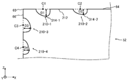
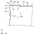
- FIG. 25 is an enlarged view of the vicinity of the tip surface 66 of the chip connection portion 52.
- the inhibition region 251 provided on the tip surface 66 and the upper surface 64 is shown, and the inhibition region 251 on the side surface 68 is omitted.
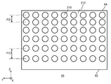
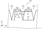
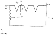
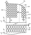
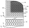
- the inhibition region 251 of this example is a region in which a plurality of recesses 210 and a plurality of flat surface portions 212 are formed on the surface of the lead frame 50.
- a step is formed on the surface of the chip connecting portion 52, and it is possible to prevent the solder 32 from getting wet and spreading.
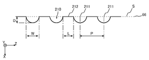
- FIG. 26 is a diagram showing an example of the recess 210 and the flat surface portion 212 on the tip surface 66.
- the inhibition region 251 formed on the other surface may also have the same structure as the inhibition region 251 of the tip surface 66.
- the recess 210 is a portion recessed from the surface S of the tip surface 66.
- the flat surface portion 212 is a portion of the tip surface 66 that remains without the recess 210 being formed.
- the plurality of flat surface portions 212 may be arranged on the same plane (on the surface S in FIG. 26).
- a flat surface portion 212 is arranged between two recesses 210 adjacent to each other in a predetermined direction.
- the plurality of recesses 210 may be arranged two-dimensionally on the tip surface 66.
- the plurality of recesses 210 may be periodically arranged along at least two directions. The period (or spacing) of the recesses 210 in one direction may or may not be constant.
- FIG. 26 shows the recesses 210 and the flat surface portion 212 arranged at regular intervals in the height direction (Z-axis direction).
- the maximum width W of each recess 210 may be 10 ⁇ m or more.
- the maximum width W refers to the maximum width of the recesses 210 on the surface S.
- the maximum width W is the diameter of the recess 210 on the surface S.
- the maximum width W is the diagonal length of the recess 210 on the surface S.
- each recess 210 may be 1 ⁇ m or more. Depth D refers to the maximum depth of the recess 210 with respect to the surface S. By increasing the depth D, the step on the surface S can be increased, and the volume of the recess 210 can be increased. As a result, it is possible to prevent the solder from getting wet and spreading.
- the depth D may be 3 ⁇ m or more, 5 ⁇ m or more, or 10 ⁇ m or more.
- the depth D may be smaller than the maximum width W and may be smaller than half of the maximum width W.
- the distance P between the centers 211 of the adjacent recesses 210 may be 10 ⁇ m or more.
- the center 211 is the center of the recess 210 on the surface S.
- the center 211 may point to the center of gravity of the geometric shape of the recess 210 on the surface S. If the interval P becomes too small, it is not possible to suppress the wetting and spreading of the solder. For example, when the interval P is smaller than the maximum width W, the recesses 210 overlap each other. In this case, the solder easily spreads over the plurality of overlapping recesses 210.
- the interval P is preferably larger than the maximum width W.
- the interval P may be 1 ⁇ m or more larger than the maximum width W, 3 ⁇ m or more, or 5 ⁇ m or more.
- the length L of the flat surface portion 212 may be 1 ⁇ m or more.
- the length L is the shortest distance between two adjacent recesses 210.
- the length L may be 3 ⁇ m or more, and may be 5 ⁇ m or more. Both the interval P and the length L may be larger than the depth D.
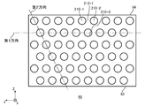
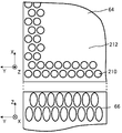
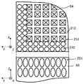
- FIG. 27 is a diagram showing an arrangement example of the recess 210 and the flat surface portion 212 on the tip surface 66.
- the number of recesses 210 arranged on the tip surface 66 is an example, and the number of recesses 210 is not limited to the illustrated example.
- the recess 210 is periodically arranged in at least two directions of the tip surface 66. In the example of FIG. 27, they are periodically arranged in two directions, a lateral direction (Y-axis direction) parallel to the lower surface 62 of the chip connecting portion 52 and a height direction (Z-axis direction) perpendicular to the lower surface 62. ..
- the lateral and height directions are perpendicular to each other.
- the flat surface portion 212 is arranged between two adjacent recesses 210 in any direction.
- the region of the tip surface 66 where the recess 210 is not formed is the flat surface portion 212.
- the flat surface portion 212 is arranged between two recesses 210 adjacent to each other in the horizontal direction and between two recesses 210 adjacent to each other in the height direction. Further, the flat surface portions 212 on the tip surface 66 may be connected to each other.
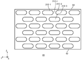
- FIG. 28 is a diagram showing another arrangement example of the recess 210 and the flat surface portion 212 on the tip surface 66.
- the tip surface 66 of this example is different from the example of FIG. 27 in the direction in which the recess 210 is periodically arranged.
- Other structures are similar to the example in FIG.
- the recesses 210 are periodically arranged along the first direction and the second direction.
- the first direction and the second direction are orthogonal to each other.
- the first and second directions intersect diagonally.
- the first direction is the Y-axis direction
- the second direction is a direction that diagonally intersects the Y-axis.
- the plurality of recesses 210 are arranged with a predetermined gap in the lateral direction (Y-axis direction) parallel to the lower surface 62 of the chip connecting portion 52.
- a flat surface portion 212 may be arranged in the gap.
- the flat surface portion 212-1 is arranged between the recess 210-1 and the recess 210-2.
- the plurality of recesses 210 include recesses 210-3 arranged side by side with the gap (planar portion 212-1) in the height direction (Z-axis direction).
- the recess 210-3 is a recess 210 adjacent to the recess 210-1 in the second direction.
- the recess 210-3 may be arranged at the center of the recess 210-1 and the recess 210-2 in the lateral direction (Y-axis direction).
- the width of the recess 210 is preferably larger than the width of the gap (flat surface portion 212-1).
- the width of the gap (flat surface portion 212-1) is the shortest distance between the two recesses 210-1 and the recess 210-2 that sandwich the gap in the lateral direction.
- FIG. 29 is a diagram showing a part of the steps in the manufacturing method of the semiconductor module 100.
- the surface of the chip connecting portion 52 specifically at least the tip surface 66, is irradiated with a laser to form a plurality of recesses 210 and a flat surface portion 212 (S341).
- S341 a plurality of recesses 210 and a flat surface portion 212 may be formed on each side surface 68 and the upper surface 64.
- soldering 32 soldering 32 (S342). Since the recess 210 and the flat surface portion 212 are formed on the tip surface 66 or the like before S342, it is possible to suppress the creeping up of the solder 32 on the tip surface 66 or the like.
- the coating layer 13 is formed (S343).
- the coating layer 13 may be formed on the surfaces of the lead frame 50 and the solder 32.
- the lead frame 50, the semiconductor chip 40, and the like may be sealed with the sealing resin 12.
- the semiconductor module 100 can be formed.
- FIG. 30 is a diagram showing the measurement results of Examples 1 to 3 and Reference Examples 1 to 3.
- the laser is irradiated so as not to overlap the surface of the chip connecting portion 52, that is, a plurality of recesses 210 and a flat surface portion 212 arranged between the two recesses 210 are formed. be.
- the shape of the recess 210 is a circle, a flat surface portion 212 is formed between the circles even if the distance P and the maximum width W are the same.
- the length L is the shortest distance between the two adjacent recesses 210, in other words, the minimum length L.
- Reference Examples 1 to 3 are obtained by superimposing a laser on the surface of the chip connection portion 52. Specifically, in Reference Examples 1 to 3, the lasers are repeatedly struck so that the flat surface portion 212 is not formed between the two recesses 210. In Reference Example 1, the interval P of laser irradiation at the time of overstrike is larger than that of Reference Example 2 and Reference Example 3.
- the solder spread in FIG. 30 is an index showing the area where the solder spread.
- the solder spread of the tip surface 66 that does not form the recess 210 is set to 0.
- the degree of spread when the solder spread is large as compared with the tip surface 66 which does not form the recess 210 is shown by a positive numerical value, and the degree of spread when the solder spread is small is shown by a negative numerical value.
- the solder spread tends to be smaller than in the case where the recesses 210 are not formed.
- the lead frame 50 described in the examples of FIGS. 24 to 29 may have the rough surface region 51 described in FIGS. 1 to 23.
- the front end surface 66 may have a rough surface region 51
- the side surface 68 may have a rough surface region 51
- the upper surface 64 may have a rough surface region 51.
- the inhibition region 251 described in FIGS. 24 to 29 may function as a rough surface region 51. That is, the inhibition region 251 may have a developed area ratio of 0.2 or more. Further, the entire tip surface 66 may have a developed area ratio of 0.2 or more.
- the rough surface region 51 may be formed on the flat surface portion 212. For example, after forming the rough surface region 51 on the tip surface 66, a plurality of recesses 210 may be formed by laser irradiation or the like. The same applies to the lead frame 50 of FIGS. 31 to 45 described below.
- the expanded area ratio of the inhibition region 251 is 0.2 or more, and the region functions as a rough surface region 51. Therefore, it is possible to hinder the wet spread of the solder and improve the adhesion between the resin such as the coating layer 13 and the lead frame 50.
- At least a part of the recesses 210 on the tip surface 66 may be in contact with the solder 32.
- a solder 32 jointing layer 32
- a part of the recess 210 on the tip surface 66 may be in contact with the coating layer 13.
- the recess 210 closest to the top surface 64 may be in contact with the coating layer 13, and the recess 210 closest to the bottom surface 62 may be in contact with the solder 32.
- FIG. 31 is a diagram illustrating laser irradiation to the chip connection portion 52.
- FIG. 31 schematically shows the vicinity of the tip surface 66 of the chip connection portion 52 and the light source 310.
- the light source 310 irradiates the surface of the chip connection portion 52 with the laser 312.
- One recess 210 can be formed by irradiating the surface of the chip connecting portion 52 with the laser 312 once. The surface remaining without the concave portion 210 being formed becomes the flat surface portion 212.
- the tip surface 66 is irradiated with a laser to form one recess 210 and a flat surface portion 212.
- FIG. 32 is a diagram showing an example of laser irradiation in S341 of FIG. 29.
- the light source 310 irradiates the surface of the chip connection portion 52 with the laser 312 without replacing the chip connection portion 52. That is, in this example, the arrangement of the chip connection portion 52 is fixed. Then, by changing the laser irradiation angle of the light source 310, the laser 312 is irradiated to a plurality of positions on the surface of the chip connection portion 52. The light source 310 sequentially irradiates the surface of the chip connection portion 52 with a plurality of lasers 312.
- a plurality of recesses 210 and a flat surface portion 212 arranged between the two recesses 210 can be formed on the surface of the chip connection portion 52, and the inhibition region 251 can be provided on the surface of the chip connection portion 52.
- a plurality of recesses 210 and a flat surface portion 212 arranged between the two recesses 210 are formed on the surface of the tip surface 66.
- the light source 310 may irradiate a plurality of lasers 312 without changing the focal position.
- the focal position may be aligned with any position of the tip surface 66.
- the shape or size of each recess 210 may be different.
- a plurality of recesses 210 and a flat surface portion 212 arranged between the two recesses 210 are formed on the surface of the tip surface 66, but the plurality of recesses 210 and the recesses 210 are formed on the surface of the upper surface 64.
- a flat surface portion 212 arranged between the two recesses 210 may be formed.
- a plurality of recesses 210 and a flat surface portion 212 arranged between the two recesses 210 are formed on the surface of the tip surface 66, and by replacing the chip connecting portion 52, a plurality of recesses are formed on the surface of the upper surface 64.
- the 210 and the flat surface portion 212 arranged between the two recesses 210 can be formed.
- replacing the chip connection portion 52 means changing the relative position of each surface of the chip connection portion 52 with respect to the light source 310.
- the surface of the chip connection portion 52 may be irradiated with the laser 312 by a plurality of light sources 310.
- one light source 310 irradiates the surface of the tip surface 66 with the laser 312, and the other one light source 310 irradiates the surface of the top surface 64 with the laser 312.
- the inhibition region 251 can be provided on the surface of the tip surface 66 and the surface of the upper surface 64.
- the light source 310 may change the irradiation angle in the YZ plane. That is, the light source 310 in FIG. 32 scans the surface of the chip connection portion 52 in one direction, but the light source 310 may scan the surface of the chip connection portion 52 in a plurality of directions.
- the light source 310 may be a device capable of irradiating a plurality of lasers 312 at the same time.
- FIG. 33 is a diagram showing another example of laser irradiation in S341 of FIG. 29.
- the light source 310 irradiates at least two surfaces of the chip connection 52 with a common light source 310 without replacing the chip connection 52.
- the laser 312 is irradiated to each surface of the chip connection portion 52 by changing the irradiation angle without changing the arrangement of the laser light source. That is, the arrangement of the chip connection portion 52 is fixed, and the light source 310 irradiates at least two surfaces of the chip connection portion 52 with a plurality of lasers 312 by changing the irradiation angle of the light source 310.
- the light source 310 may sequentially irradiate the surface of the chip connection portion 52 with a plurality of lasers 312. By doing so, a plurality of recesses 210 and a flat surface portion 212 arranged between the two recesses 210 are formed on at least two surfaces of the chip connection portion 52, and at least two surfaces of the chip connection portion 52 are formed. Can be provided with an inhibition region 251. In this example, a plurality of recesses 210 and a flat surface portion 212 arranged between the two recesses 210 are formed on the surface of the tip surface 66 and the surface of the upper surface 64.
- the light source 310 irradiates the laser 312 diagonally to each surface of the chip connection portion.
- the light source 310 obliquely irradiates the surface of the tip surface 66 and the surface of the upper surface 64 with all the lasers 312. That is, the laser 312 is not irradiated perpendicularly to the surface of the tip surface 66 and the surface of the upper surface 64.
- the laser 312 By irradiating the laser 312 diagonally, it is possible to irradiate at least two surfaces of the chip connection 52 with a common light source 310 without replacing the chip connection 52.
- the light source 310 may irradiate each surface of the chip connection portion 52 with a plurality of lasers 312 without changing the focal position. By irradiating the plurality of lasers 312 without changing the focal position, the plurality of lasers 312 can be continuously irradiated, and the processing time can be shortened.
- the focal position is set to, for example, the angle 65.
- the corner 65 is a portion where the two surfaces of the chip connecting portion 52 intersect. In the example of FIG. 33, the portion where the upper surface 64 and the tip surface 66 intersect is a corner 65.
- the focal position may be adjusted to any position of the tip surface 66.
- the focal position may be aligned with any position on the upper surface 64.
- the depth of the recess 210 becomes deeper.
- the focal position may be adjusted to the angle 65. By deeply forming the recess 210 in the vicinity of the corner 65, it is possible to suppress the peeling of the chip connecting portion 52 and the sealing resin 12 in the vicinity of the corner 65 where stress is likely to be concentrated. Further, the focal position may be adjusted to the tip surface 66. By deepening the recess 210 formed in the tip surface 66, it is possible to prevent the solder from creeping up on the tip surface 66.
- FIGS. 34 and 35 are views showing another example of laser irradiation in S341 of FIG. 29.
- the position of the light source 310 is different from that in FIG. 33.
- the light source 310 is provided on the front end surface 66 side as compared with FIG. 33.
- the light source 310 is provided on the upper surface 64 side as compared with FIG. 33.
- FIG. 36 is a diagram showing an example of the surface shape of the concave portion 210 of the tip surface 66 and the upper surface 64. 36 shows an example of the surface shape of the recess 210 of FIGS. 34 and 35. Further, in FIG. 36, the length in the longitudinal direction of the surface shape of the recess 210 on the tip surface 66 (Z-axis direction in FIGS. 34 and 35) is L1, and the length in the longitudinal direction of the surface shape of the recess 210 on the upper surface 64 (FIG. 34). , The length in the X-axis direction of FIG. 35) is L2.
- the light source 310 is provided on the front end surface 66 side as compared with FIG. 33. Therefore, the angle formed by the lasers 312 incident on the upper surface 64 and the upper surface 64 is smaller than that in FIG. 33. Therefore, the length L2 in the longitudinal direction of the surface shape of the recess 210 on the upper surface 64 is larger than the length L1 in the longitudinal direction of the surface shape of the recess 210 on the tip surface 66. In this example, L1 / L2 is 0.5.
- the light source 310 is provided on the upper surface 64 side as compared with FIG. 33. Therefore, the angle formed by the laser 312 incident on the tip surface 66 and the tip surface 66 is smaller than that in FIG. 33. Therefore, the length L1 in the longitudinal direction of the surface shape of the recess 210 on the tip surface 66 is larger than the length L2 in the longitudinal direction of the surface shape of the recess 210 on the upper surface 64. In this example, L1 / L2 is 1.2.
- L1 / L2 may be 0.5 or more.
- L1 / L2 may be 1.2 or less.
- FIG. 37 is a diagram illustrating the shapes of the recesses 210 of the tip surface 66 and the upper surface 64.
- the upper surface 64 is provided with a recess 210-1 and a recess 210-2.
- the recess 210-1 is provided on the tip surface 66 side of the recess 210-2.
- the center of the recess 210-1 in the X-axis direction is C1
- the center of the recess 210-1 in the X-axis direction is C2.
- the tip surface 66 is provided with a recess 210-3 and a recess 210-4.
- the recess 210-3 is provided on the upper surface 64 side of the recess 210-4.
- the center of the recess 210-3 in the Z-axis direction is C3, and the center of the recess 210-4 in the Z-axis direction is C4.
- the laser 312 is obliquely irradiated to each surface of the chip connection portion 52. Therefore, the position of the bottom portion 314 of the recess 210 deviates from the center of the recess 210.
- the bottom portion 314 of at least one recess 210 formed on the upper surface 64 is arranged on the side opposite to the tip surface 66 of the chip connecting portion 52 from the center of the recess 210. That is, the bottom portion 314-1 of the recess 210-1 is arranged on the opposite side of the tip surface 66 from the center C1 of the recess 210-1.
- the bottom portion 314-2 of the recess 210-2 is arranged on the side opposite to the tip surface 66 from the center C2 of the recess 210-2.
- the bottom portion 314 of at least one recess 210 formed on the tip surface 66 may be arranged on the side opposite to the top surface 64 of the chip connection portion from the center of the recess 210. That is, the bottom portion 314-3 of the recess 210-3 may be arranged on the opposite side of the upper surface 64 from the center C3 of the recess 210-3. The bottom portion 314-4 of the recess 210-4 may be arranged on the side opposite to the upper surface 64 from the center C4 of the recess 210-4. The bottom portion 314 of at least one recess 210 formed on the tip surface 66 may be arranged substantially in line with the center of the recess 210.
- the depth of the recess 210 becomes shallower as the distance from the angle 65 increases. Therefore, the depth of the recess 210 formed on the upper surface 64 becomes shallower as the distance from the tip surface 66 increases.
- the depth of the recess 210 is the depth at the bottom 314.
- the depth D2 of the recess 210-2 is smaller than the depth D1 of the recess 210-1.
- the depth of the recess 210 formed in the tip surface 66 becomes shallower as the distance from the upper surface 64 increases. That is, the depth D4 of the recess 210-4 is smaller than the depth D3 of the recess 210-3.
- the recesses 210 formed in FIGS. 33, 34 and 35 are the same on the upper surface 64 and the tip surface 66, respectively, but the recesses 210 formed in FIGS. 33, 34 and 35 are also the recesses 210 of FIG. 37. May have the shape of. That is, in FIGS. 33, 34 and 35, the bottom portion 314 of at least one recess 210 formed on the upper surface 64 is arranged on the side opposite to the tip surface 66 of the chip connecting portion 52 from the center of the recess 210. It is also good. In FIGS.
- the bottom portion 314 of at least one recess 210 formed on the tip surface 66 may be arranged on the side opposite to the top surface 64 of the chip connection portion from the center of the recess 210.
- the depth of the recess 210 formed in the upper surface 64 may become shallower as the distance from the tip surface 66 increases.
- only the recess 210 formed in the tip surface 66 may have the shape of the recess 210 in FIG. 37.
- FIGS. 38, 39, 40 and 41 are views showing an example of the arrangement of the recesses 210 of the upper surface 64 and the tip surface 66.
- the recess 210 may be arranged in a straight line as shown in FIG. 38.
- the recesses 210 may be arranged in a grid pattern as shown in FIG. 39. Further, as shown in FIGS. 40 and 41, the recess 210 may not have the recess 210 arranged on the entire upper surface 64.
- the recess 210 is arranged only in the vicinity of the tip surface 66 and the side surface 68 on the upper surface 64.
- FIGS. 38, 39, 40 and 41 the arrangement of the recesses 210 of the upper surface 64 and the tip surface 66 is shown, but the recesses 210 may be arranged in the lower surface 62 and the tip surface 66.
- FIG. 42 is a diagram showing another arrangement example of the recess 210 and the flat surface portion 212 on the tip surface 66.
- the shape of the recess 210 of the tip surface 66 of this example is different from that of FIG. 27 or FIG. 28.
- Other structures are similar to the example of FIG. 27 or FIG.
- the width of the recess 210 in this example in the lateral direction is larger than the width in the height direction (Z-axis direction). According to this example, the path from the lower surface 62 to the upper surface 64 can be lengthened through the flat surface portion 212. Therefore, it is possible to further suppress the creeping up of the solder.
- the recess 210 may have a shape such as an oval, an ellipse, or a rectangle on the tip surface 66.
- the width of the recess 210 in the lateral direction may be 1.5 times or more, may be 2 times or more, and may be 3 times or more the width in the height direction.
- a plurality of recesses 210 are provided in the lateral direction. That is, the lateral width of the recess 210 is smaller than half the lateral width of the tip surface 66.
- FIG. 43 is a diagram showing another arrangement example of the recess 210 and the flat surface portion 212 on the tip surface 66.
- the shape of the recess 210 of the tip surface 66 of this example is different from that of the example of FIG. 27, FIG. 28, or FIG. 42.
- Other structures are similar to the example of FIG. 27, FIG. 28, or FIG. 42.
- the shape of the recess 210 on the tip surface 66 has the recess 214.
- the recessed portion 214 is a portion in which the end side of the recessed portion 210 on the lower surface 62 side is recessed on the upper surface 64 side.
- the flat surface portion 212 in contact with the recessed portion 214 is surrounded by the recessed portion 210 in three directions, the upper side and both sides in the lateral direction. Therefore, it is possible to prevent the solder that has reached the recessed portion 214 from creeping up to the upper surface 64 side.
- FIG. 44 is a diagram showing another arrangement example of the recess 210 and the flat surface portion 212 on the tip surface 66.
- the tip surface 66 of this example is different from the example of FIG. 27, FIG. 28, FIG. 42 or FIG. 43 in the arrangement of the recess 210.
- Other structures are similar to the examples of FIGS. 27, 28, 42 or 43.
- the density of the plurality of recesses 210 in the lateral direction is higher than the density of the plurality of recesses 210 in the height direction (Z-axis direction).
- the density of the recesses 210 may be the reciprocal of the spacing between two adjacent recesses 210 in each direction.
- the distance between the recesses 210 is the distance P described in FIG.
- the spacing PY of the recesses 210 in the lateral direction is smaller than the spacing PZ of the recesses 210 in the height direction.
- the interval PZ may be 1.5 times or more the interval PY, and may be 2 times or more. According to this example, since the distance PY in the lateral direction of the recesses 210 is small, it is possible to prevent the solder from passing between the two recesses 210 arranged in the lateral direction.
- FIG. 45 is a diagram showing another arrangement example of the recess 210 and the flat surface portion 212 on the tip surface 66.
- the tip surface 66 of this example differs from the example of FIGS. 27, 28 or 42 to 44 in the arrangement of the recesses 210.
- Other structures are similar to any example of FIG. 27, FIG. 28 or FIGS. 42-44.
- the density of the plurality of recesses 210 in the height direction is higher as the distance from the lower surface 62 is higher.
- the spacing PZs of a pair of recesses 210 adjacent to each other in the height direction the spacing of the pair closest to the upper surface 64 is PZ1 and the spacing of the pair closest to the lower surface 62 is PZ2.
- the interval PZ2 is larger than the interval PZ1.
- the interval PZ2 may be 1.5 times or more the interval PZ1 and may be 2 times or more. According to this example, since the spacing PZ of the recesses 210 in the vicinity of the upper surface 64 is small, the closer to the upper surface 64, the more the solder can be suppressed from creeping up.
- the tip surface 66 has been illustrated and described.
- the inhibition region 251 is provided on each side surface 68 as well as the tip surface 66. That is, it is preferable to form a plurality of recesses 210 and a flat surface portion 212 on the tip surface 66, each side surface 68, and the upper surface 64 to form the inhibition region 251.
- the lead frame 50 described in the examples of FIGS. 31 to 45 may also have the rough surface region 51 described in FIGS. 1 to 23.
- the inhibition region 251 may function as a rough surface region 51.
- FIG. 46 is a diagram showing a part of the steps in the manufacturing method of the semiconductor module 100.
- the shape is transferred to the surface of the chip connecting portion 52, specifically, the upper surface 64 of the chip connecting portion 52 by a mold, and a plurality of recesses 210 and a flat surface portion 212 are formed in an obstruction region 251. (S441).
- soldering 32 soldering 32 (S442). Since the recess 210 and the flat surface portion 212 are formed on the tip surface 66 or the like in front of S442, it is possible to suppress the creeping up of the solder 32 on the tip surface 66 or the like.
- S442 may be the same process as S342 in FIG.
- the coating layer 13 is formed (S443).
- the coating layer 13 may be formed on the surfaces of the lead frame 50 and the solder 32.
- the lead frame 50, the semiconductor chip 40, and the like may be sealed with the sealing resin 12.
- the semiconductor module 100 can be formed.
- S443 may be the same process as S343 in FIG.
- FIG. 47 is a diagram illustrating shape transfer to the chip connection portion 52 by the mold 320.
- the mold 320 transfers the shape to the surface of the chip connection portion 52.
- the concave portion 210 and the flat surface portion 212 can be formed.
- the shape is transferred to the upper surface 64 to form three recesses 210 and a flat surface portion 212. That is, in this example, the three recesses 210 are mold holes formed by press working. The press working to form the three recesses 210 does not have to extrude the lower surface 62, which is the opposite surface of the upper surface 64.
- the shape of the lower surface 62 of the chip connecting portion 52 does not change and may remain flat.
- the protrusion 88 is formed by press working, the upper surface 64 may be recessed, and the concave portion of the upper surface 64 and the lower surface 62 may be pushed out to form a convex portion to be the protrusion 88.
- the mold 320 has a first portion 322 and a second portion 324.
- the mold 320 can transfer the shape of the first portion 322.
- the first portion 322 is, for example, a square thrust shape.
- the first portion 322 preferably has a shape in which it is easy to pull out the first portion 322 after transferring the shape.
- the second portion 324 connects to the three first portions 322.
- the concave portion 210 and the flat surface portion 212 are formed by pressing with the mold 320 and compressing the chip connecting portion 52. Therefore, the recess 210 is compressed as compared to other surfaces.
- the recess 210 may be compressed from the flat surface portion 212.
- the fact that the recess 210 is compressed may mean that the hardness of the recess 210 is higher than that of other surfaces.
- the fact that the recess 210 is compressed may mean that the density of the recess 210 is higher than that of other surfaces.
- the surface of the chip connecting portion 52 may be a rough surface region having a developed area ratio of 0.1 or more. Further, the surface of the chip connecting portion 52 may be a rough surface region having a developed area ratio of 0.4 or less, preferably 0.35 or less, and more preferably 0.3 or less.
- FIG. 48 is a diagram showing an example of the arrangement of the recess 210 and the flat surface portion 212 on the upper surface 64.
- the recess 210 may be arranged in a straight line as shown in FIG. 48.
- the shape of the upper surface of the recess 210 may be polygonal. In this example, the shape of the upper surface of the recess 210 is a quadrangular shape.
- FIG. 49 is a diagram for explaining in detail the shapes of the recess 210 and the flat surface portion 212 on the upper surface 64.
- FIG. 49 shows the shapes of the recess 210 and the flat surface portion 212 formed by the mold.
- the flat surface portion 212 has a raised portion 216 and a standard portion 218.
- the raised portion 216 is formed adjacent to the recess 210.
- the raised portion 216 is a portion having the same height as the standard portion 218 in the height direction or a portion raised in the height direction from the standard portion 218. In this example, the raised portion 216 is raised in the height direction from the standard portion 218.
- the standard portion 218 is a portion whose height has not changed from the surface before forming the recess 210, for example.
- the standard part 218 is adjacent to the raised part 216.
- the standard portion 218 may be recessed in the height direction from the raised portion 216. Further, at least a part of the recess 210 is recessed from the standard portion 218 in the height direction.
- the raised portion 216 is sandwiched between the recess 210 and the standard portion 218.
- the heights in the respective height directions may be compared and discriminated.
- the difference d1 in the height direction between the standard portion 218 and the recess 210 is larger than the difference d2 in the height direction between the raised portion 216 and the standard portion 218 (which may be the depth of the recess 210).
- d2 may be 30% or less of d1.
- d2 may be 20% or less of d1.
- d2 is smaller than d1, the raised portion 216, the standard portion 218 and the concave portion 210 can be discriminated.
- a portion that looks flat when observing the upper surface 64 see, for example, FIG. 48
- D1 may be 20 ⁇ m or more. d1 may be 200 ⁇ m or less. d1 may be more preferably 50 ⁇ m or more and 150 ⁇ m or less. Further, the width d3 of the recess 210 may be 50 ⁇ m or more. d3 may be 250 ⁇ m or less. d3 is more preferably 100 ⁇ m or more and 200 ⁇ m or less. Further, the pitch width d4 of the recess 210 may be 200 ⁇ m or more. d4 may be 700 ⁇ m or less. d4 is more preferably 300 ⁇ m or more and 600 ⁇ m or less. Further, the minimum length d7 of the flat surface portion 212 may be 150 ⁇ m or more.
- d7 may be 450 ⁇ m or less. d7 is more preferably 200 ⁇ m or more and 400 ⁇ m or less.
- the minimum length d7 may be a length obtained by extending the standard portion 218 in the horizontal direction (X-axis direction or Y-axis direction). In FIG. 49, the minimum length d7 of the flat surface portion 212 is defined as the minimum length between the recesses 210 when the standard portion 218 is extended in the horizontal direction (X-axis direction or Y-axis direction). However, the minimum length d7 may be approximated to the minimum length of the portion where the recess 210 is not formed when viewed in a plan view.
- the shapes of the recess 210 and the flat portion 212 formed by the mold are shown, but the recess 210 and the flat portion 212 formed by laser irradiation may also have the same shape. That is, the flat surface portion 212 formed by laser irradiation may have a raised portion 216 and a standard portion 218.
- d1 is, for example, 10 ⁇ m.
- a plurality of recesses 210 and a flat surface portion 212 may be formed on the tip surface 66, each side surface 68, and the upper surface 64 to form an inhibition region 251.
- the inhibition region 251 may be configured only on the upper surface 64.
- the lead frame 50 described in the examples of FIGS. 46 to 49 may also have the rough surface region 51 described in FIGS. 1 to 23.
- the inhibition region 251 may function as a rough surface region 51.
- the rough surface region 51 may be formed by using a roughening liquid.
- the roughening liquid may be commercially available.
- a mask may be used for the surface that does not form the rough surface region 51, or the entire surface may be roughened without using the mask.
- FIG. 50 is a diagram showing a part of the steps in the manufacturing method of the semiconductor module 100.
- the shape is transferred to the surface of the chip connecting portion 52, specifically, the upper surface 64 of the chip connecting portion 52 by a mold to form a plurality of recesses 210 and a flat surface portion 212 (S541).
- S541 may be the same process as S441 in FIG.
- the surface of the chip connection portion 52 is irradiated with a laser to form a plurality of recesses 210 and a flat surface portion 212 to form an obstruction region.
- 251 is provided (S542).
- a plurality of recesses 210 and a flat surface portion 212 may be formed on each side surface 68 and the upper surface 64.
- soldering 32 soldering 32 (S543). Since the recess 210 and the flat surface portion 212 are formed on the tip surface 66 or the like before S543, it is possible to suppress the creeping up of the solder 32 on the tip surface 66 or the like.
- S543 may be the same process as S342 in FIG.
- the coating layer 13 is formed (S544).
- the coating layer 13 may be formed on the surfaces of the lead frame 50 and the solder 32.
- the lead frame 50, the semiconductor chip 40, and the like may be sealed with the sealing resin 12.
- the semiconductor module 100 can be formed.
- S544 may be the same process as S343 in FIG.
- FIG. 51 is a diagram illustrating the shape of the chip connection portion 52.
- the shape is transferred to the upper surface 64 of the chip connection portion 52 by the mold.
- the tip surface 66 of the chip connection portion 52 is irradiated with a laser. Therefore, the recess 210 formed on the upper surface 64 is a mold hole. Further, the recess 210 formed in the tip surface 66 is a laser hole.
- the depth of the mold hole is deeper than the depth of the laser hole. That is, the depth d5 of the recess 210 formed on the upper surface 64 is deeper than the depth d6 of the recess 210 formed on the tip surface 66.
- Such a configuration can be obtained by providing a mold hole on the upper surface 64 and a laser hole on the tip surface 66.
- FIG. 52 is a diagram showing another example of the arrangement of the recess 210 and the flat surface portion 212 on the upper surface 64 and the tip surface 66.
- the upper surface 64 and the tip surface 66 are shown in common in the Y-axis direction.
- the recess 210 is formed by irradiating the tip surface 66 and the upper surface 64 of the chip connecting portion 52 with a laser 312 at an angle.
- the recess 210 formed by laser irradiation is arranged only in the vicinity of the front end surface 66 and the side surface 68.
- a recess 210 formed by a mold is arranged on the upper surface 64.
- the recess 210 formed by laser irradiation has a curved line.
- the recess 210 formed by laser irradiation is circular. Further, the shape of the concave portion 210 on the tip surface 66 has a curved line. Further, the recess 210 formed by the mold has a polygonal shape. In this example, the recess 210 formed by the mold has a rectangular shape.
- the laser is irradiated so as to overlap at least a part of the plurality of recesses 210 whose shape is transferred by the mold. That is, on the upper surface, at least a part of the recess 210 formed by the laser irradiation and the recess 210 formed by the mold overlap.
- the inhibition region 251 can be provided on the entire surface of the upper surface 64.
- FIG. 53 is a diagram showing an example of arrangement of recesses 210 on the upper surface 64, the tip surface 66, and the lower surface 62.
- the upper surface 64, the tip surface 66, and the lower surface 62 are shown in common in the Y-axis direction.
- the recess 210 is formed by irradiating the tip surface 66 and the lower surface 62 of the chip connecting portion 52 with a laser 312 obliquely.
- a recess 210 formed by a mold is arranged on the upper surface 64. With such an arrangement, the inhibition region 251 can be provided on the upper surface 64, the tip surface 66, and the lower surface 62.
- each side surface 68 may form an inhibition region 251 in the same manner as the tip surface 66.
- a plurality of recesses 210 and a flat surface portion 212 are formed on the tip surface 66, each side surface 68, and the upper surface 64 to form an inhibition region 251.
- the inhibition region 251 may be configured only on the upper surface 64.
- the lead frame 50 described in the examples of FIGS. 50 to 53 may also have the rough surface region 51 described in FIGS. 1 to 23.
- the inhibition region 251 may function as a rough surface region 51.
- the region of the upper surface 64 on which the mold hole is formed is preferably a developed area ratio of 0.1 or more.
- the developed area ratio of the region of the tip surface 66 and each side surface 68 on which the laser hole is formed is preferably 0.2 or more.
- laser roughening and mold roughening are used in combination
- present embodiment is not limited to this.
- laser roughening and liquid roughening may be used in combination
- mold roughening and liquid roughening may be used in combination.
- FIG. 54 is a diagram showing another example of the arrangement of the inhibition region 251.
- FIG. 54 shows an example of the arrangement of the inhibition region 251 on the upper surface 64 of the chip connection portion 52.
- the inhibition region 251 is shown by hatching.
- the plurality of recesses 210 are periodically arranged in at least two directions on at least one surface of the chip connection 52. Then, any surface of the chip connecting portion 52 has an unprocessed portion 336 whose periodic arrangement is interrupted.
- the unprocessed portion 336 may be a flat surface portion 212.
- FIG. 55 is a diagram showing an example of the arrangement of the recesses 210 of the upper surface 64 and the tip surface 66 in FIG. 54.
- FIG. 55 shows the arrangement of the plurality of recesses 210 and the flat surface portion 212.
- the inhibition region 251 may be formed by forming the plurality of recesses 210 and the flat surface portion 212.
- the inhibition region 251 may function as a rough surface region 51. That is, the inhibition region 251 may have any of the structures and functions described as the rough surface region 51 in addition to the structure and function described as the inhibition region 251.
- a plurality of recesses 210 and a flat surface portion 212 are formed on the upper surface 64 of the chip connecting portion 52. Further, as shown in FIG. 55, a plurality of recesses 210 and a flat surface portion 212 are formed on the tip surface 66 of the chip connecting portion 52. Although not shown, a plurality of recesses 210 and a flat surface portion 212 may be formed on the side surface 68 of the chip connecting portion 52 as in the tip surface 66.
- the edge farthest from the bridge portion 54 is defined as the edge 181.
- the upper surface 64 is a substantially rectangular shape having two sets of two parallel sides, but may have other shapes.
- the end edge of the upper surface 64 may be a straight line.
- the end side 181 is connected to the tip surface 66. That is, the upper surface 64 and the tip surface 66 are connected by the end side 181.
- the end edge closest to the bridge portion 54 is referred to as an end edge 182.
- the end side 182 is connected to the side surface 68. That is, the upper surface 64 and the side surface 68 are connected by an end side 182.
- the side between the end side 181 and the end side 182 is defined as the end side 183.
- the end side 183 is connected to the side surface 68. That is, the upper surface 64 and the side surface 68 are connected by the end side 183.
- the end side 181 and the end side 183 may be connected by a curved line in a top view.
- the plurality of recesses 210 and the flat surface portion 212 are formed by laser roughening.
- the plurality of recesses 210 and the flat surface portion 212 may be formed by roughening the mold.
- the plurality of recesses 210 and the flat surface portion 212 may be formed by liquid roughening.
- the inhibition region 251 is not provided near the end side 181 and the end side 183. That is, the raw portion 336 may be provided in the vicinity of the end side 181 and the end side 183.
- the shortest distance A1 between the recess 210 and the end side 181 is larger than the distance A3 between the adjacent recesses 210.
- the distance A3 between the adjacent recesses 210 may be the minimum length of the flat surface portion 212 (d7 in the example of FIG. 49).
- the shortest distance A1 may be 2 times or more, 5 times or more, or 10 times or more the interval A3. Further, in FIG.
- the shortest distance A2 between the recess 210 and the end side 183 is larger than the distance A3 between the adjacent recesses 210.
- the shortest distance between the recess 210 formed on the upper surface 64 and at least one end of the surface (upper surface 64) may be larger than the distance A3 between the adjacent recesses 210.
- the shortest distance A2 may be 5 times or more, 10 times or more, or 20 times or more the interval A3.
- FIG. 56 is a diagram showing an example of the chip connection portion 52 according to the comparative example. If the inhibition region 251 is provided near the end edge of the upper surface 64 (end edge 181 in the example of FIG. 56), one recess 210-5 is formed on both the upper surface 64 and the tip surface 66 (or the side surface 68). There is. If the recess 210-5 is provided, the solder tends to get wet and spread from the front end surface 66 (or the side surface 68) to the upper surface 64. In the examples of FIGS.
- the developed area ratio of the upper surface 64 in which the plurality of recesses 210 are formed is preferably 0.7 or less.
- the shortest distance A1 between the recess 210 and the end side 181 may be 0.3 mm or more and 1.5 mm or less.
- the shortest distance A2 of the end side 183 with the recess 210 may be 0.3 mm or more and 1.5 mm or less.
- the distance A3 between the adjacent recesses 210 may be 30 ⁇ m or more and 60 ⁇ m or less.
- the shortest distance A1 between the recess 210 and the end side 181 may be larger than the thickness of the chip connecting portion 52 in the Z-axis direction.
- the shortest distance A2 between the recess 210 and the end side 183 may be larger than the thickness of the chip connecting portion 52 in the Z-axis direction.
- the thickness of the chip connecting portion 52 in the Z-axis direction may be 0.3 mm or more, preferably 0.5 mm or more.
- the shortest distance A1 between the recess 210 formed on the upper surface 64 of the chip connecting portion and the end side 181 may be larger than the shortest distance between the recess 210 formed on the tip surface 66 of the chip connecting portion 52 and the end side 181.
- the recess 210 may be provided in the vicinity of the end side 181 on the tip surface 66 of the chip connecting portion 52.
- the shortest distance A2 between the recess 210 formed on the upper surface 64 of the chip connecting portion and the end side 183 as in the tip surface 66 is the shortest distance between the recess 210 formed on the side surface 68 of the chip connecting portion 52 and the end side 183. It may be larger than (not shown).
- the recess 210 may not be provided in the vicinity of the end side 181 on the tip surface 66 of the chip connecting portion 52. That is, the shortest distance between the recess 210 formed on the tip surface 66 of the chip connecting portion 52 and the end side 181 may be larger than the distance A3 between the adjacent recesses 210.
- FIG. 57 is a diagram showing another example of the arrangement of the inhibition region 251.
- FIG. 57 differs from FIG. 54 in that the inhibition region 251 is not provided near the edge 182. That is, the unprocessed portion 336 may be provided in the vicinity of the end side 182.
- Other configurations of FIG. 57 may be the same as those of FIG. 54.
- the shortest distance A8 between the recess 210 and the end side 182 may be larger than the distance A3 between the adjacent recesses 210 (see FIG. 55).
- the shortest distance A8 between the recess 210 and the end side 182 may be 0.3 mm or more and 1.5 mm or less.
- FIG. 58 is a diagram showing another example of the arrangement of the inhibition region 251.
- FIG. 58 shows an example of the arrangement of the inhibition region 251 on the upper surface 64 of the chip connection portion 52.
- the inhibition region 251 is shown by hatching.
- FIG. 59 is a diagram showing an example of the arrangement of the recesses 210 of the upper surface 64 and the tip surface 66 in FIG. 58.
- FIG. 59 shows the arrangement of the plurality of recesses 210 and the flat surface portion 212.
- the inhibition region 251 may be formed by forming the plurality of recesses 210 and the flat surface portion 212.
- the inhibition region 251 may function as a rough surface region 51.
- the plurality of recesses 210 and the flat surface portion 212 are formed by laser roughening.
- the end side 183-1 faces the end side 183-2.
- the end side 183-1 is an example of the first end side.
- the end side 183-2 is an example of the second end side.
- the end side 181 is an example of the third end side.
- the inhibition region 251 is not provided near the center line CL of the upper surface 64 of the chip connection portion 52. That is, the unprocessed portion 336 may be provided in the vicinity of the center line CL.
- the center line CL is a line passing through the center C of the upper surface 64 of the chip connecting portion 52.
- the center line CL is parallel to the X-axis direction.
- the center C of the upper surface 64 of the chip connecting portion 52 may be the center in the XY plane of the upper surface 64 of the chip connecting portion 52, or may be the center of gravity of the upper surface 64 of the chip connecting portion 52.
- the maximum distance A4 within the distance between the recesses 210 sandwiched between the edge 183-1 and the edge 1832 is the first shortest of the recess 210 formed on the upper surface 64 of the chip connection portion 52 and the edge 183-1. It is larger than the distance A5 (see FIG. 59). Further, the maximum distance A4 within the distance between the concave portions 210 sandwiched between the end side 183-1 and the end side 183-2 is the second of the concave portion 210 and the end side 183-2 formed on the upper surface 64 of the chip connecting portion 52. 2 Greater than the shortest distance (not shown).
- FIG. 60 is a diagram illustrating laser irradiation to the chip connection portion 52 according to the comparative example.
- laser irradiation is performed on at least two surfaces of the chip connection portion 52 with a common light source 310 without replacing the chip connection portion 52 as shown in FIG. 33, for example, toward the end side 183-1 and the end side 183-2.
- the laser irradiation spots overlap each other in the vicinity of the center line CL of the upper surface 64 of the chip connection portion 52.
- the solder tends to get wet and spread in the vicinity of the center line CL of the upper surface 64 of the chip connecting portion 52.
- the inhibition region 251 is not provided near the center line CL of the upper surface 64 of the chip connecting portion 52, the spots of laser irradiation overlap each other in the vicinity of the center line CL of the upper surface 64 of the chip connecting portion 52. Can be prevented. Therefore, it is possible to suppress the wetting and spreading of the solder.
- the maximum distance A4 within the distance between the recesses 210 sandwiched between the end side 183-1 and the end side 183-2 may be, for example, 0.3 mm or more and 1.5 mm or less.
- the first shortest distance A5 between the recess 210 formed on the upper surface 64 of the chip connecting portion 52 and the end side 183-1 may be 30 ⁇ m or more and 60 ⁇ m or less.
- the second shortest distance between the recess 210 formed on the upper surface 64 of the chip connecting portion 52 and the end side 183-2 may be 30 ⁇ m or more and 60 ⁇ m or less.
- the distance between the recesses 210 in the center C between the end sides 183-1 and the end sides 183-2 of the upper surface 64 of the chip connecting portion 52 may be larger than the first shortest distance A5 and the second shortest distance.
- the maximum distance A4 among the distances between the recesses 210 sandwiched between the end sides 183-1 and the end sides 183-2 may be the distance between the recesses 210 at the center C. That is, the distance between the recesses 210 may be maximum at the center C between the end sides 183-1 and the end sides 183-2. Further, the distance between the recesses 210 does not have to be the maximum in the center C.
- the shortest distance A6 between the recess 210 formed on the upper surface 64 of the chip connecting portion 52 and the end side 181 is larger than the first shortest distance A5. Further, the shortest distance A6 between the recess 210 formed on the upper surface 64 of the chip connecting portion 52 and the end side 181 is larger than the second shortest distance. Therefore, since the obstruction region 251 is not provided in the vicinity of the end side 181 it is possible to suppress the wetting and spreading of the solder.
- the shortest distance A6 between the recess 210 formed on the upper surface 64 of the chip connecting portion 52 and the end side 181 is larger than the shortest distance A7 between the recess 210 formed on the tip surface 66 of the chip connecting portion 52 and the end side 181. That is, on the tip surface 66, the inhibition region 251 is provided in the vicinity of the end side 181. By providing the obstruction region 251 in the vicinity of the end side 181 on the tip surface 66, it is possible to suppress the wetting and spreading of the solder.
- the shortest distance A7 between the recess 210 formed on the tip surface 66 of the chip connecting portion 52 and the end side 181 may be larger than the distance A3 between the adjacent recesses 210.
- FIG. 61 is a diagram showing another example of the arrangement of the inhibition region 251.
- FIG. 61 differs from FIG. 58 in that the inhibition region 251 is provided in the vicinity of the end side 182.
- Other configurations of FIG. 61 may be the same as those of FIG. 58. Even with such a configuration, it is possible to suppress the wetting and spreading of the solder.
- FIG. 62 is a diagram showing another example of the arrangement of the inhibition region 251.
- FIG. 62 differs from FIG. 58 in that the inhibition region 251 is not provided near the edge 183. That is, the unprocessed portion 336 may be provided in the vicinity of the end side 183.
- Other configurations of FIG. 62 may be the same as those of FIG. 58. Even with such a configuration, it is possible to suppress the wetting and spreading of the solder.
- FIG. 63 is a diagram showing another example of the arrangement of the inhibition region 251.
- FIG. 63 shows an example of the arrangement of the inhibition region 251 on the upper surface 64 of the chip connection portion 52.
- the inhibition region 251 has an overlapping portion 332 and a non-overlapping portion 334, which are shown by different hatchings.
- FIG. 64 is a diagram showing an example of the arrangement of the recesses 210 of the upper surface 64 and the tip surface 66 in FIG. 63.
- FIG. 64 shows the arrangement of the plurality of recesses 210 and the flat surface portion 212.
- the inhibition region 251 may be formed by forming the plurality of recesses 210 and the flat surface portion 212.
- the inhibition region 251 may function as a rough surface region 51.
- the overlapping portion 332 can be formed by controlling the spot of laser irradiation (irradiation position of laser irradiation).
- the arrangement of the recesses 210 in the overlapping portion 332 may be the irradiation position of the laser irradiation.
- the overlapping portion 332 does not have to have a flat surface portion 212 arranged between the two recesses 210. That is, it may not function as the inhibition region 251 but may function as the rough surface region 51.
- overlapping portion 332 adjacent recesses 210 overlap.
- a recess 210 is further provided between the adjacent recesses 210.
- the overlapping portion 332 may be formed by further irradiating the flat surface portion 212 arranged between the adjacent recesses 210 with a laser.
- the overlapping portion 332 may be a portion where adjacent recesses 210 are continuous.
- the overlapping portion 332 may or may not be provided with the flat surface portion 212.
- a flat surface portion 212 is provided between adjacent recesses 210.
- the overlapping portion 332 can have a larger developed area ratio than the non-overlapping portion 334.
- the solder is more likely to get wet and spread than in the non-overlapping portion 334.
- the overlapping portion 332 is provided inside the surface (upper surface 64) as compared with the non-overlapping portion 334. That is, the overlapping portion 332 is not provided in the vicinity of the end side 181, the end side 182, and the end side 183 of the upper surface 64.
- FIG. 65 is a diagram illustrating the shape of the overlapping portion 332.
- the recess 210 is formed on the upper surface 64 and the tip surface 66 of the chip connecting portion 52 by laser irradiation.
- the recess 210 in this example is a laser hole. Further, by overlapping the irradiation positions of the laser irradiation, the overlapping portion 332 is formed on the upper surface 64 of the chip connecting portion 52.
- the depth d7 of the recess 210 provided in the overlapping portion 332 is deeper than the depth d8 of the recess 210 provided in the non-overlapping portion 334.
- the depth d7 may be 1.5 times or more the depth d8.
- the depth d7 of the recess 210 provided in the overlapping portion 332 is deeper than the depth d9 of the recess 210 formed in the tip surface 66.
- the depth d7 may be 1.5 times or more the depth d9. Since the recess 210 provided in the overlapping portion 332 is deeper than the recess 210 provided in other than the overlapping portion 332, the overlapping portion 332 and the non-overlapping portion 334 can be distinguished.
- FIGS. 54 to 65 the inhibition region 251 of the chip connecting portion 52 has been illustrated and described, but the above-described configuration may be applied to the circuit pattern connecting portion 56 and other surfaces.
- FIG. 66 is a diagram showing another example of the lead frame 50.
- the lead frame 50 of this example differs from the example of FIGS. 1 to 34 in that the chip connecting portion 52 has a main material portion 231 and an obstructing portion 230.
- Other structures may be identical to any of the forms described in FIGS. 1-34.
- the main material portion 231 is a portion formed of the same material as the lower surface 62. When a plurality of types of material portions are exposed on the lower surface 62, the main material portion 231 is formed of the same material as the portion having the largest area on the lower surface 62.
- the main material portion 231 is a portion formed of, for example, copper or an alloy containing copper.
- the main material portion 231 may be a portion formed of the same material as the crosslinked portion 54.
- the obstruction portion 230 is a portion formed of a material having a lower solder wettability than the main material portion 231. That is, the obstruction portion 230 is a portion where the solder is less likely to spread than the main material portion 231.
- the inhibitory portion 230 is, for example, a portion formed of ceramic, carbon, aluminum, an alloy containing aluminum, iron, or an alloy containing iron.
- the obstructing portion 230 is exposed on the tip surface 66 of the chip connecting portion 52. As a result, it is possible to suppress the creeping up of the solder on the tip surface 66.
- the obstruction portion 230 may be exposed on the side surface 68 of the chip connection portion 52.
- the chip connecting portion 52 may be formed of a clad material in which a main material portion 231 and an obstructing portion 230 are laminated.
- the chip connecting portion 52 may be provided with an obstructing portion 230 between the two main material portions 231.
- FIG. 67 is a diagram showing an arrangement example of the main material portion 231 and the obstruction portion 230 in the chip connecting portion 52.
- the obstruction portion 230 is hatched with diagonal lines. Further, the obstruction portion 230 covered by the main material portion 231 is also shown to pass through the main material portion 231.
- the plate-shaped main material portion 231 and the plate-shaped obstructing portion 230 are laminated in the height direction.
- the plate shape refers to a shape in which the area of the main surface substantially parallel to the upper surface 64 is substantially perpendicular to the upper surface 64 and is larger than the area of any side surface.
- the chip connecting portion 52 shown in FIG. 67 has a main material portion 231-1 exposed on the upper surface 64, a main material portion 231-2 exposed on the lower surface 62, and an obstruction portion 230 sandwiched between the two main material portions 231. Have.
- the obstruction portion 230 is exposed on the tip surface 66 and each side surface 68.
- the obstructing portion 230 is exposed so as to cross each surface at a predetermined height position on each surface. That is, in the lateral direction, the width of the obstructing portion 230 is the same as the width of each surface. With such a shape, it is possible to suppress the creeping up of the solder on the tip surface 66 and each side surface 68.
- the widths of the main material portion 231-1, the main material portion 231-2, and the obstruction portion 230 in the height direction are Z1, Z2, and Z3, respectively.
- the inhibitory portion 230 may have the same width Z3 on the tip surface 66 and each side surface 68.
- the main material portion 231-1 may also have the same width Z1 on the tip surface 66 and each side surface 68.
- the main material portion 231-2 may also have the same width Z2 on the tip surface 66 and each side surface 68.
- the width Z3 of the obstructing portion 230 is larger than either the width Z1 of the main material portion 231-1 or the width Z2 of the main material portion 231-2.
- the width Z3 may be larger than the sum of the widths Z1 and the width Z2. This makes it easier to suppress the creeping up of the solder on each surface.
- the width Z1 may be the same as the width Z2, may be large, or may be small.
- FIG. 68 is a diagram showing another example of the lead frame 50. This example differs from the examples of FIGS. 66 and 67 in that the inhibitory portion 230 is exposed on the upper surface 64. Other structures are similar to the examples in FIGS. 66 and 67.
- FIG. 69 is an enlarged schematic view of the chip connection portion 52 of FIG. 68.
- the inhibitory portion 230 of this example is exposed on the upper surface 64.
- the obstruction portion 230 may be exposed to the entire upper surface 64.
- the chip connecting portion 52 of this example does not have the main material portion 231-1 shown in FIG. 67.
- FIG. 70 is a diagram showing another example of the lead frame 50.
- the shape of the inhibitory portion 230 is different from the example of FIGS. 66 to 69.
- Other structures are similar to any of the examples in FIGS. 66-69.
- the obstruction portion 230 of this example is exposed on the lower surface 62.
- FIG. 71 is a diagram showing an example of arrangement of the obstructing portion 230 on the lower surface 62 of the chip connecting portion 52.
- the obstruction portion 230 of this example is arranged on the lower surface 62 outside the protrusion 88.
- the outside of the protrusion 88 refers to the area between the protrusion 88 and the tip surface 66 or the side surface 68.
- the blocking portion 230 may be in contact with the tip surface 66.
- the obstruction portion 230 may be exposed on the tip surface 66.
- the inhibitory portion 230 may be in contact with the side surface 68.
- the inhibitory portion 230 may be exposed on the side surface 68.
- the obstruction portion 230 may be separated from the protrusion portion 88. According to this example, it is possible to suppress the creeping up of the solder on the front end surface 66 and the side surface 68 while wetting most of the lower surface 62 with the solder.
- FIG. 72 is an enlarged schematic view of the chip connection portion 52 of FIGS. 70 and 71.
- the inhibitory portion 230 of this example is exposed on the lower surface 62.
- the obstruction portion 230 is exposed on the tip surface 66 and each side surface 68.
- the obstruction portion 230 of this example has a frame shape surrounding a predetermined region.
- FIG. 73 is a diagram showing another arrangement example of the obstructing portion 230 on the lower surface 62 of the chip connecting portion 52.
- the obstruction portion 230 of this example is arranged on the lower surface 62 outside the protrusion 88. However, the obstructing portion 230 is not in contact with the tip surface 66. That is, the obstructing portion 230 is not exposed on the tip surface 66.
- the blocking portion 230 is not in contact with the side surface 68. That is, the obstructing portion 230 is not exposed on the side surface 68.
- the obstruction portion 230 may be separated from the protrusion portion 88. Also in this example, it is possible to suppress the creeping up of the solder on the front end surface 66 and the side surface 68 while wetting most of the lower surface 62 with the solder.
- FIG. 74 is a diagram showing another arrangement example of the main material portion 231 and the obstruction portion 230 in the chip connecting portion 52.
- FIG. 74 shows the obstruction portion 230 not covered by the main material portion 231.
- the obstruction portion 230 of this example differs from the example of FIGS. 66 to 73 in that the obstruction portion 230 projects outward from the main material portion 231 in the direction perpendicular to the tip surface 66 of the chip connection portion 52 (X-axis direction). do.
- Other structures are similar to any of the examples of FIGS. 66-73.
- the obstructing portion 230 may protrude outward from the main material portion 231.
- the inhibitory portion 230 may have a plate shape as shown in FIG. 67 or FIG. 69. In this case, the area of the obstructing portion 230 on the XY surface is larger than the area of the main material portion 231.
- the inhibitory portion 230 may have a frame shape as shown in FIG. 72. In this case, the main material portion 231 has a portion surrounded by the obstructing portion 230.
- the main material portion 231 may have a recess in any one of the front end surface 66 and the side surface 68 into which a part of the obstruction portion 230 is inserted.
- FIG. 75 is a diagram showing another arrangement example of the main material portion 231 and the obstruction portion 230 in the chip connecting portion 52.
- FIG. 75 shows the obstruction portion 230 not covered by the main material portion 231.
- the obstruction portion 230 of this example differs from the example of FIGS. 66 to 73 in that the obstruction portion 230 is recessed inward from the main material portion 231 in the direction perpendicular to the tip surface 66 of the chip connection portion 52 (X-axis direction). do.
- Other structures are similar to any of the examples of FIGS. 66-73.
- the obstructing portion 230 may be recessed inward from the main material portion 231.
- the inhibitory portion 230 may have a plate shape as shown in FIG. 67 or FIG. 69. In this case, the area of the obstructing portion 230 on the XY surface is smaller than the area of the main material portion 231.
- the inhibitory portion 230 may have a frame shape as shown in FIG. 72. In this case, the main material portion 231 has a portion surrounded by the obstructing portion 230.
- FIG. 76 is a diagram showing another arrangement example of the main material portion 231 and the obstruction portion 230 in the chip connecting portion 52.
- the obstruction portion 230 covered by the main material portion 231 is also shown through the main material portion 231.
- the obstruction portion 230 of this example is laminated on the surface of the main material portion 231.
- the obstruction portion 230 is laminated with the main material portion 231 on the tip surface 66 of the chip connecting portion 52 in a direction perpendicular to the tip surface 66.
- the blocking portion 230 may also be laminated on each side surface 68.
- the inhibition portion 230 is formed by laminating a predetermined material on the surface of the main material portion 231 by a method such as sputtering or thermal spraying.
- the region where the obstruction portion 230 is exposed on each surface of the chip connection portion 52 is the same as any of the examples described with reference to FIGS. 66 to 75. Also in this example, it is possible to suppress the creeping up of the solder on the tip surface 66 and the like.
- the inhibitory portion 230 may be formed of ceramic such as aluminum oxide, aluminum nitride, or silicon nitride, may be formed of carbon, or may be formed of a metal such as iron.
- the grain shape of the material irradiated to the main material portion 231 may be controlled. Thereby, the roughness of the surface of the obstruction portion 230 can be controlled.
- a rough surface region 51 may be formed on the surface of the obstruction portion 230. Further, the rough surface region 51 may be formed in the main material portion 231.
- the wiring part is A chip connection portion connected to the semiconductor chip and The circuit pattern connection part connected to the circuit pattern and It has a chip connection portion and a cross-linking portion that connects the circuit pattern connection portion.
- the chip connection portion has a lower surface facing the semiconductor chip and has a lower surface. The lower surface of the chip connection portion has a first side farthest from the cross-linking portion.
- the lower surface of the chip connection portion has a second side closest to the crosslinked portion.
- the semiconductor module according to item 1 wherein the inclination or the step is provided along a side other than the second side among the sides of the lower surface of the chip connection portion.
- a plurality of protrusions protruding toward the semiconductor chip are provided on the lower surface of the chip connection portion.
- the step is provided on the lower surface of the chip connection portion.
- Item 2 The item 1 to 3, wherein the step includes at least one of a protrusion protruding from the lower surface toward the circuit pattern and a groove recessed from the lower surface in a direction away from the circuit pattern.
- Semiconductor module. (Item 5) Item 4. The semiconductor module according to item 4, wherein the step is the protruding portion and is provided in contact with the first side.
- Item 6) Item 4. The semiconductor module according to item 4, wherein the step is the groove portion and is provided in contact with the first side.
- Item 7) The semiconductor module according to item 4, wherein the step is the groove portion and is provided apart from the first side.
- the lower surface of the chip connection portion is provided with the inclination.
- the semiconductor module according to any one of items 1 to 3, wherein the inclination is chamfered at a corner of the lower surface.
- the wiring portion has a chip connection portion to be connected to the semiconductor chip, and the wiring portion has a chip connection portion.
- the chip connection is Main material part and A semiconductor module formed of a material having a lower solder wettability than the main material portion and having an obstruction portion exposed and arranged on the tip surface.
Landscapes
- Structures Or Materials For Encapsulating Or Coating Semiconductor Devices Or Solid State Devices (AREA)
- Lead Frames For Integrated Circuits (AREA)
Abstract
Description
特許文献1 WO2017/163583
図1は、本発明の一つの実施形態に係る半導体モジュール100の一例を示す図である。半導体モジュール100は、インバータ等の電力変換装置として機能してよい。半導体モジュール100は、1つ以上の絶縁回路基板160を備える。本明細書では、1つ以上の絶縁回路基板160が設けられる面における直交軸をX軸およびY軸とし、XY面と垂直な軸をZ軸とする。図1においては、XY面における各部材の配置例を示している。
本例の半導体モジュール100は、それぞれがU層、V層、W層のアームを構成する3つの絶縁回路基板160を備えている。絶縁回路基板160には、1つ以上の半導体チップ40が載置される。半導体チップ40は、絶縁回路基板160を囲む樹脂ケース10や樹脂ケース10に充填される封止樹脂12といった樹脂パッケージ14により保護される。
図4は、図3のリードフレーム50の拡大図である。リードフレーム50は、表面の少なくとも一部分において、粗面領域51を有する。図4においては、粗面領域51が設けられた表面を、破線で示している。粗面領域51は、展開面積比(Sdr)が0.2以上の領域である。
[測定環境の例]
測定器:キーエンス社製VK-X1100
コントローラ―部:キーエンス社製VK-X1000
対物レンズ:Apo×50倍
カットオフ:ガウシアン
Sフィルター:なし
Lフィルター:なし
F-オペレーション:なし
図8は、リードフレーム50の他の構造例を示す斜視図である。本例では、チップ接続部52において、半導体チップ40と向かい合う下面62には、段差70が設けられていることが好ましい。また、回路パターン接続部56の下面にも、チップ接続部52と同様の段差70が設けられてよい。なお、図8のリードフレーム50では、チップ接続部52、回路パターン接続部56には、突起部88は設けられない。
図22は、参考例に係るチップ接続部152を示す図である。チップ接続部152は、粗面領域51が設けられていない点を除き、チップ接続部52と同一の構造を有する。チップ接続部152の先端面66または側面68は、はんだ濡れ性を有する。このため、先端面66または側面68に沿って、はんだ32が這い上がる場合がある。
図29は、半導体モジュール100の製造方法における一部の工程を示す図である。本例では、チップ接続部52の表面、具体的には少なくとも先端面66に対してレーザー照射し、複数の凹部210と、平面部212を形成する(S341)。S341においては、各側面68および上面64にも、複数の凹部210と平面部212を形成してよい。
図46は、半導体モジュール100の製造方法における一部の工程を示す図である。本例では、チップ接続部52の表面、具体的にはチップ接続部52の上面64に対して金型により形状を転写し、複数の凹部210と、平面部212とが形成された阻害領域251を設ける(S441)。
レーザー照射および金型による粗面領域51の形成方法について説明したが、粗面領域51は、粗化液を用いて、形成してもよい。粗化液は、市販のものであってよい。粗化液を用いる場合、粗面領域51を形成しない表面にはマスクを用いてもよいし、マスクを用いずに全面粗化してもよい。
図50は、半導体モジュール100の製造方法における一部の工程を示す図である。本例では、チップ接続部52の表面、具体的にはチップ接続部52の上面64に対して金型により形状を転写し、複数の凹部210と、平面部212を形成する(S541)。S541は、図46のS441と同一の工程であってよい。
図54は、阻害領域251の配置の他の例を示す図である。図54において、チップ接続部52の上面64における阻害領域251の配置の一例を示している。図54では、阻害領域251をハッチングで示している。阻害領域251の配置の他の例では、複数の凹部210が、チップ接続部52の少なくともいずれかの面の少なくとも2つの方向において周期的に配置されている。そして、チップ接続部52のいずれかの面は、周期的な配置が途切れた未加工部336を有する。なお、未加工部336は、平面部212であってよい。
図66は、リードフレーム50の他の例を示す図である。本例のリードフレーム50は、チップ接続部52が、主材部231および阻害部230を有する点で、図1から図34の例と相違する。他の構造は、図1から図34において説明したいずれかの形態と同一であってよい。
(項目1)
一方の面に回路パターンが形成された絶縁回路基板と、
前記絶縁回路基板に載置された半導体チップと、
前記半導体チップと前記回路パターンとを接続する配線部と、
前記半導体チップを保護する樹脂パッケージと
を備え、
前記配線部は、
前記半導体チップと接続するチップ接続部と、
前記回路パターンと接続する回路パターン接続部と、
前記チップ接続部および前記回路パターン接続部を接続する架橋部と
を有し、
前記チップ接続部は、前記半導体チップと向かい合う下面を有し、
前記チップ接続部の前記下面は、前記架橋部から最も離れた第1の辺を有し、
前記チップ接続部の前記下面には、前記第1の辺の半分以上の長さにわたって、前記第1の辺に沿った段差または傾斜が設けられている
半導体モジュール。
(項目2)
前記チップ接続部の前記下面は、前記架橋部に最も近い第2の辺を有し、
前記傾斜または段差は、前記チップ接続部の前記下面の辺のうち、前記第2の辺以外の辺に沿って設けられている
項目1に記載の半導体モジュール。
(項目3)
前記チップ接続部の前記下面には、前記半導体チップに向かって突出する複数の突起部が設けられていて、
前記突起部の高さは、前記段差または前記傾斜よりも低い
項目1または2に記載の半導体モジュール。
(項目4)
前記チップ接続部の前記下面には、前記段差が設けられていて、
前記段差は、前記下面から前記回路パターンに向かって突出した突出部、および、前記下面から前記回路パターンから離れる方向に窪んだ溝部の少なくとも一方を含む
項目1から3のいずれか一項に記載の半導体モジュール。
(項目5)
前記段差は、前記突出部であって、前記第1の辺に接して設けられている
項目4に記載の半導体モジュール。
(項目6)
前記段差は、前記溝部であって、前記第1の辺に接して設けられている
項目4に記載の半導体モジュール。
(項目7)
前記段差は、前記溝部であって、前記第1の辺から離れて設けられている
項目4に記載の半導体モジュール。
(項目8)
前記チップ接続部の前記下面には、前記傾斜が設けられていて、
前記傾斜は、前記下面の角部を面取りしている
項目1から3のいずれか一項に記載の半導体モジュール。
(項目9)
一方の面に回路パターンが形成された絶縁回路基板と、
前記絶縁回路基板に載置された半導体チップと、
前記半導体チップおよび前記回路パターンを電気的に接続する配線部と
を備え、
前記配線部は、前記半導体チップと接続するチップ接続部を有し、
前記チップ接続部は、
主材部と、
前記主材部よりもはんだ濡れ性が低い材料で形成され、先端面において露出して配置された阻害部と
を有する半導体モジュール。
Claims (68)
- 一方の面に回路パターンが形成された絶縁回路基板と、
前記絶縁回路基板に載置された半導体チップと、
前記半導体チップおよび前記回路パターンを電気的に接続する配線部と
を備え、
前記配線部は、前記半導体チップと接続するチップ接続部を有し、
前記チップ接続部の表面は、
複数の凹部と、
2つの凹部の間に配置された平面部と
を有する半導体モジュール。 - それぞれの前記凹部の最大幅が10μm以上である
請求項1に記載の半導体モジュール。 - 隣り合う前記凹部の中心の間隔が10μm以上である
請求項1または2に記載の半導体モジュール。 - 前記半導体チップと前記チップ接続部を接合する接合層を更に備え、
前記複数の凹部の少なくとも一部において、前記凹部の内部に前記接合層が設けられている
請求項1から3のいずれか一項に記載の半導体モジュール。 - 前記複数の凹部が形成された前記表面は、展開面積比が0.2以上である粗面領域を有する
請求項1から4のいずれか一項に記載の半導体モジュール。 - 前記複数の凹部が形成された前記表面は、展開面積比が0.7以下である粗面領域を有する
請求項1から5のいずれか一項に記載の半導体モジュール。 - 前記複数の凹部は、前記チップ接続部の少なくともいずれかの面の少なくとも2つの方向において周期的に配置されていて、
前記チップ接続部のいずれかの面は、前記周期的な配置が途切れた未加工部を有する
請求項1から6のいずれか一項に記載の半導体モジュール。 - 少なくとも前記チップ接続部の先端面に、前記複数の凹部と前記平面部とが形成されている
請求項1から7のいずれか一項に記載の半導体モジュール。 - 前記複数の凹部は、前記先端面の少なくとも2つの方向において周期的に配置されている
請求項8に記載の半導体モジュール。 - 前記複数の凹部は、前記チップ接続部の下面と平行な横方向において、予め定められた間隙を有して配置されており、
前記複数の凹部は、前記横方向と垂直な高さ方向において、前記間隙と並んで配置された凹部を含む
請求項9に記載の半導体モジュール。 - 前記横方向において、前記凹部の幅は、前記間隙の幅よりも大きい
請求項10に記載の半導体モジュール。 - 前記凹部は、前記チップ接続部の下面と平行な横方向における幅が、前記横方向と垂直な高さ方向における幅よりも大きい
請求項9から11のいずれか一項に記載の半導体モジュール。 - 前記チップ接続部の下面と平行な横方向における前記複数の凹部の密度は、前記横方向と垂直な高さ方向における前記複数の凹部の密度よりも高い
請求項9から12のいずれか一項に記載の半導体モジュール。 - 前記チップ接続部の下面と垂直な高さ方向における前記複数の凹部の密度は、前記下面から遠いほど高い
請求項9から13のいずれか一項に記載の半導体モジュール。 - 前記チップ接続部は、
主材部と、
前記主材部よりもはんだ濡れ性が低い材料で形成され、前記先端面において露出して配置された阻害部と
を有する請求項8から14のいずれか一項に記載の半導体モジュール。 - 前記先端面において、前記チップ接続部の下面と垂直な高さ方向における前記阻害部の幅は、前記高さ方向における前記主材部の幅より大きい
請求項15に記載の半導体モジュール。 - 前記阻害部は、前記チップ接続部の下面と垂直な高さ方向において、前記主材部と積層されている
請求項15または16に記載の半導体モジュール。 - 前記阻害部は、前記チップ接続部の先端面と垂直な方向において、前記主材部と積層されている
請求項15または16に記載の半導体モジュール。 - 前記阻害部は、前記チップ接続部の前記先端面と垂直な方向において、前記主材部よりも突出または窪んでいる
請求項15から18のいずれか一項に記載の半導体モジュール。 - 前記チップ接続部の先端面、側面および上面に、前記複数の凹部および前記平面部が形成されている
請求項8から19のいずれか一項に記載の半導体モジュール。 - 前記配線部は、板状の部分を有するリードフレームであって、
前記平面部は、
標準部と、
前記チップ接続部の表面と垂直な高さ方向の高さが、前記標準部と同じかまたは前記標準部より高さ方向に隆起した隆起部と
を有し、
前記凹部の少なくとも一部は、前記高さ方向において前記標準部より窪んで配置されていて、
前記隆起部は、前記凹部に隣接して設けられる
請求項1に記載の半導体モジュール。 - 前記複数の凹部が形成された前記表面は、展開面積比が0.1以上である粗面領域を有する
請求項21に記載の半導体モジュール。 - それぞれの前記凹部の深さが、20μm以上でかつ200μm以下ある、
請求項21に記載の半導体モジュール。 - 前記チップ接続部の上面に、前記複数の凹部および前記平面部が形成されている
請求項22または23に記載の半導体モジュール。 - 前記チップ接続部の先端面に、前記複数の凹部および前記平面部が形成されていて、
前記上面に形成された少なくとも1つの前記凹部の深さは、前記先端面に形成された少なくとも1つの前記凹部の深さよりも深い
請求項24に記載の半導体モジュール。 - 前記複数の凹部は、金型孔を含む
請求項21に記載の半導体モジュール。 - 前記複数の凹部は、レーザー孔を含む
請求項26に記載の半導体モジュール。 - 前記チップ接続部の上面に、前記複数の凹部および前記平面部が形成されていて、
それぞれの前記凹部の前記上面における形状は、多角形状である
請求項21に記載の半導体モジュール。 - 前記チップ接続部の先端面に、前記複数の凹部および前記平面部が形成されていて、
それぞれの前記凹部の前記先端面における形状は、曲線を有する
請求項28に記載の半導体モジュール。 - 前記凹部は、前記平面部より圧縮されている
請求項21に記載の半導体モジュール。 - 前記チップ接続部の上面および先端面に、前記複数の凹部および前記平面部が形成されていて、
前記上面に形成された少なくとも1つの前記凹部の底部は、当該前記凹部の中心より前記チップ接続部の先端面と逆側に配置されている
請求項21に記載の半導体モジュール。 - 前記上面に形成された前記凹部の深さは、前記先端面と離れるに従って、浅くなる
請求項31に記載の半導体モジュール。 - 前記凹部と前記表面の少なくとも1つの端辺の最短距離は、隣り合う前記凹部の間隔より大きい
請求項24に記載の半導体モジュール。 - 前記チップ接続部の先端面に、前記複数の凹部および前記平面部が形成されていて、
前記チップ接続部の前記上面および前記チップ接続部の前記先端面は、端辺で接続していて、
前記チップ接続部の前記上面に形成された前記凹部と前記端辺の最短距離は、前記チップ接続部の前記先端面に形成された前記凹部と前記端辺の最短距離より大きい
請求項33に記載の半導体モジュール。 - 前記チップ接続部の側面に、前記複数の凹部および前記平面部が形成されていて、
前記チップ接続部の前記上面および前記チップ接続部の前記側面は、端辺で接続していて、
前記チップ接続部の前記上面に形成された前記凹部と前記端辺の最短距離は、前記チップ接続部の前記側面に形成された前記凹部と前記端辺の最短距離より大きい
請求項33または34に記載の半導体モジュール。 - 前記表面には、
隣り合う前記凹部が重なる重なり部と、
隣り合う前記凹部の間に前記平面部が設けられる非重複部と
が設けられ、
前記重なり部は、前記非重複部と比べ、前記表面の内側に設けられる
請求項1から6のいずれか一項に記載の半導体モジュール。 - 前記チップ接続部の上面に、前記複数の凹部および前記平面部が形成されていて、
前記上面は、第1端辺と、前記第1端辺と対向する第2端辺とを有し、
前記第1端辺および前記第2端辺に挟まれた前記凹部の間隔の内の最大距離は、前記チップ接続部の前記上面に形成された前記凹部と前記第1端辺の第1最短距離および前記チップ接続部の前記上面に形成された前記凹部と前記第2端辺の第2最短距離よりも大きい
請求項1から6のいずれか一項に記載の半導体モジュール。 - 前記チップ接続部の前記上面の前記第1端辺および前記第2端辺の間の中央における前記凹部の間隔は、前記第1最短距離および前記第2最短距離よりも大きい
請求項37に記載の半導体モジュール。 - 前記チップ接続部の前記上面の前記第1端辺および前記第2端辺の間の中央において、前記凹部の間隔が前記最大距離となる
請求項37または38に記載の半導体モジュール。 - 前記上面は、前記第1端辺および前記第2端辺と接する第3端辺を更に有し、
前記チップ接続部の前記上面に形成された前記凹部と前記第3端辺の最短距離は、前記第1最短距離および前記第2最短距離よりも大きい
請求項37から39のいずれか一項に記載の半導体モジュール。 - 前記チップ接続部の先端面に、前記複数の凹部および前記平面部が形成されていて、
前記チップ接続部の前記上面および前記チップ接続部の前記先端面は、前記第3端辺で接続していて、
前記チップ接続部の前記上面に形成された前記凹部と前記第3端辺の最短距離は、前記チップ接続部の前記先端面に形成された前記凹部と前記第3端辺の最短距離より大きい
請求項40に記載の半導体モジュール。 - 一方の面に回路パターンが形成された絶縁回路基板と、
前記絶縁回路基板に載置された半導体チップと、
表面の少なくとも一部分において展開面積比が0.2以上である粗面領域を有し、前記半導体チップと前記回路パターンとを接続する配線部と、
前記半導体チップを保護する樹脂パッケージと
を備える半導体モジュール。 - 前記粗面領域の前記展開面積比は、前記回路パターンの前記展開面積比よりも大きい
請求項42に記載の半導体モジュール。 - 前記回路パターンの前記展開面積比は0.08以下である
請求項43に記載の半導体モジュール。 - 前記粗面領域の算術平均高さは10μm以下である
請求項42から44のいずれか一項に記載の半導体モジュール。 - 前記粗面領域の最大高さは100μm以下である
請求項42から45のいずれか一項に記載の半導体モジュール。 - 前記配線部は、板状の部分を有するリードフレームであって、
前記半導体チップと接続するチップ接続部と、
前記回路パターンと接続する回路パターン接続部と、
前記チップ接続部および前記回路パターン接続部を接続する架橋部と
を有し、
前記粗面領域が前記チップ接続部に設けられている
請求項42から46のいずれか一項に記載の半導体モジュール。 - 前記チップ接続部の面積が、前記回路パターン接続部の面積より大きい
請求項47に記載の半導体モジュール。 - 前記回路パターン接続部の前記展開面積比は、前記チップ接続部の前記粗面領域の前記展開面積比よりも小さい
請求項47または48に記載の半導体モジュール。 - 前記架橋部は、開口部を有する
請求項47から49のいずれか一項に記載の半導体モジュール。 - 前記チップ接続部の下面または前記回路パターン接続部の下面が、前記絶縁回路基板に向かって突出する突起部を有する
請求項47から50のいずれか一項に記載の半導体モジュール。 - 前記リードフレームの表面の少なくとも一部を覆う、樹脂で形成されたコーティング層を更に備える
請求項47から51のいずれか一項に記載の半導体モジュール。 - 前記チップ接続部は、前記架橋部から最も離れた先端面を有し、
前記先端面に前記コーティング層が設けられている
請求項52に記載の半導体モジュール。 - 前記コーティング層の膜厚は、1μm以上、100μm以下である
請求項52または53に記載の半導体モジュール。 - 前記コーティング層の表面は、前記粗面領域の凹凸に応じた凹凸を有する
請求項52から54のいずれか一項に記載の半導体モジュール。 - 前記コーティング層の表面は、前記粗面領域よりも平坦である
請求項52から55のいずれか一項に記載の半導体モジュール。 - 前記樹脂パッケージは、前記絶縁回路基板を囲む樹脂ケースと、前記樹脂ケースに充填される封止樹脂と
を含む請求項42から56のいずれか一項に記載の半導体モジュール。 - 前記チップ接続部は、前記半導体チップと向かい合う下面を有し、
前記チップ接続部の前記下面は、前記架橋部から最も離れた第1の辺を有し、
前記チップ接続部の前記下面には、前記第1の辺の半分以上の長さにわたって、前記第1の辺に沿った段差または傾斜が設けられている
請求項47から56のいずれか一項に記載の半導体モジュール。 - 一方の面に回路パターンが形成された絶縁回路基板と、前記絶縁回路基板に載置された半導体チップと、前記半導体チップおよび前記回路パターンを電気的に接続する配線部とを備え、前記配線部は、前記半導体チップと接続するチップ接続部を有する半導体モジュールの製造方法であって、
前記チップ接続部の表面に対してレーザー照射し、複数の凹部と、2つの凹部の間に配置された平面部とを形成する
製造方法。 - 前記チップ接続部の少なくとも2つの表面に対して共通の光源で前記配線部の置き換えなしにレーザー照射し、それぞれの表面に、複数の凹部と、2つの凹部の間に配置された平面部とを形成する
請求項59に記載の製造方法。 - 前記チップ接続部のそれぞれの表面に対して、斜めにレーザー照射する
請求項60に記載の製造方法。 - 前記チップ接続部のそれぞれの表面に対して、焦点位置を変えずにレーザー照射する
請求項60または61に記載の製造方法。 - 前記チップ接続部のそれぞれの表面に対して、レーザー光源の配置を変えずに照射角度を変更することでレーザー照射する
請求項60から62のいずれか一項に記載の製造方法。
製造方法。 - 前記チップ接続部の上面に対して、金型により形状を転写し、複数の凹部と、2つの凹部の間に配置された平面部とを形成し、
前記金型により形状を転写した後、前記チップ接続部の少なくとも先端面に対してレーザー照射し、複数の凹部と、2つの凹部の間に配置された平面部とを形成する
請求項59に記載の製造方法。 - 前記チップ接続部の上面に対してレーザー照射し、複数の凹部と、2つの凹部の間に配置された平面部とを形成する
請求項64に記載の製造方法。 - 前記金型により形状を転写した前記複数の凹部の少なくとも一部に重なるように、レーザー照射する
請求項65に記載の製造方法。 - 一方の面に回路パターンが形成された絶縁回路基板と、前記絶縁回路基板に載置された半導体チップと、前記半導体チップおよび前記回路パターンを電気的に接続する配線部とを備え、前記配線部は、前記半導体チップと接続するチップ接続部を有する半導体モジュールの製造方法であって、
前記チップ接続部の上面に対して、金型により形状を転写し、複数の凹部と、2つの凹部の間に配置された平面部とを形成する
製造方法。 - 前記金型は、四角錐形状を有する
請求項67に記載の製造方法。
Priority Applications (5)
| Application Number | Priority Date | Filing Date | Title |
|---|---|---|---|
| CN202180006896.2A CN114787991A (zh) | 2020-06-30 | 2021-06-29 | 半导体模块以及半导体模块的制造方法 |
| JP2021577113A JP7028391B1 (ja) | 2020-06-30 | 2021-06-29 | 半導体モジュールおよび半導体モジュールの製造方法 |
| DE112021000169.8T DE112021000169B4 (de) | 2020-06-30 | 2021-06-29 | Halbleitermodul und verfahren zum herstellen eines halbleitermoduls |
| JP2022021029A JP7767970B2 (ja) | 2020-06-30 | 2022-02-15 | 半導体モジュール |
| US17/746,889 US20220278039A1 (en) | 2020-06-30 | 2022-05-17 | Semiconductor module and method for manufacturing semiconductor module |
Applications Claiming Priority (6)
| Application Number | Priority Date | Filing Date | Title |
|---|---|---|---|
| JP2020113562 | 2020-06-30 | ||
| JP2020-113562 | 2020-06-30 | ||
| JP2020183102 | 2020-10-30 | ||
| JP2020-183102 | 2020-10-30 | ||
| JP2021039453 | 2021-03-11 | ||
| JP2021-039453 | 2021-03-11 |
Related Child Applications (1)
| Application Number | Title | Priority Date | Filing Date |
|---|---|---|---|
| US17/746,889 Continuation US20220278039A1 (en) | 2020-06-30 | 2022-05-17 | Semiconductor module and method for manufacturing semiconductor module |
Publications (1)
| Publication Number | Publication Date |
|---|---|
| WO2022004758A1 true WO2022004758A1 (ja) | 2022-01-06 |
Family
ID=79316618
Family Applications (1)
| Application Number | Title | Priority Date | Filing Date |
|---|---|---|---|
| PCT/JP2021/024649 Ceased WO2022004758A1 (ja) | 2020-06-30 | 2021-06-29 | 半導体モジュールおよび半導体モジュールの製造方法 |
Country Status (5)
| Country | Link |
|---|---|
| US (1) | US20220278039A1 (ja) |
| JP (2) | JP7028391B1 (ja) |
| CN (1) | CN114787991A (ja) |
| DE (1) | DE112021000169B4 (ja) |
| WO (1) | WO2022004758A1 (ja) |
Cited By (4)
| Publication number | Priority date | Publication date | Assignee | Title |
|---|---|---|---|---|
| JPWO2023189265A1 (ja) * | 2022-03-28 | 2023-10-05 | ||
| WO2024075445A1 (ja) * | 2022-10-06 | 2024-04-11 | 富士電機株式会社 | 半導体モジュール、半導体装置、及び車両 |
| WO2024090029A1 (ja) * | 2022-10-25 | 2024-05-02 | 富士電機株式会社 | 半導体モジュール、半導体装置、及び車両 |
| WO2024150668A1 (ja) * | 2023-01-12 | 2024-07-18 | ローム株式会社 | 半導体装置 |
Families Citing this family (7)
| Publication number | Priority date | Publication date | Assignee | Title |
|---|---|---|---|---|
| KR102866060B1 (ko) | 2021-09-03 | 2025-09-30 | 다이니폰 인사츠 가부시키가이샤 | 리드 프레임 및 그 제조 방법 |
| WO2023210170A1 (ja) * | 2022-04-25 | 2023-11-02 | 富士電機株式会社 | 半導体装置 |
| WO2024095712A1 (ja) * | 2022-11-04 | 2024-05-10 | 富士電機株式会社 | 半導体モジュール |
| WO2024095710A1 (ja) * | 2022-11-04 | 2024-05-10 | 富士電機株式会社 | 半導体モジュール |
| JP7848886B2 (ja) * | 2022-11-04 | 2026-04-21 | 富士電機株式会社 | 半導体モジュール |
| CN119096365A (zh) * | 2022-11-04 | 2024-12-06 | 富士电机株式会社 | 半导体模块和半导体模块的制造方法 |
| JPWO2025115059A1 (ja) * | 2023-11-27 | 2025-06-05 |
Citations (6)
| Publication number | Priority date | Publication date | Assignee | Title |
|---|---|---|---|---|
| JP2006202885A (ja) * | 2005-01-19 | 2006-08-03 | Mitsubishi Electric Corp | 半導体装置 |
| JP2008211168A (ja) * | 2007-01-31 | 2008-09-11 | Mitsubishi Electric Corp | 半導体装置および半導体モジュール |
| JP2017073406A (ja) * | 2014-02-24 | 2017-04-13 | 三菱電機株式会社 | 電極リードおよび半導体装置 |
| JP2017139304A (ja) * | 2016-02-03 | 2017-08-10 | 三菱電機株式会社 | 電極端子、半導体装置及び電力変換装置 |
| JP2017191857A (ja) * | 2016-04-13 | 2017-10-19 | 株式会社デンソー | 電子装置及びその製造方法 |
| JP6466625B1 (ja) * | 2017-09-05 | 2019-02-06 | 新電元工業株式会社 | 半導体装置 |
Family Cites Families (24)
| Publication number | Priority date | Publication date | Assignee | Title |
|---|---|---|---|---|
| US6521982B1 (en) * | 2000-06-02 | 2003-02-18 | Amkor Technology, Inc. | Packaging high power integrated circuit devices |
| JP3602453B2 (ja) * | 2000-08-31 | 2004-12-15 | Necエレクトロニクス株式会社 | 半導体装置 |
| US7859089B2 (en) * | 2006-05-04 | 2010-12-28 | International Rectifier Corporation | Copper straps |
| JP2009004435A (ja) * | 2007-06-19 | 2009-01-08 | Toshiba Corp | 半導体装置 |
| US7868430B2 (en) * | 2008-09-26 | 2011-01-11 | Infineon Technologies Ag | Semiconductor device |
| JPWO2012014382A1 (ja) * | 2010-07-27 | 2013-09-09 | パナソニック株式会社 | 半導体装置 |
| JP2012081481A (ja) | 2010-10-07 | 2012-04-26 | Toyota Industries Corp | 電子部品における電極の接続構造 |
| JP2013118322A (ja) * | 2011-12-05 | 2013-06-13 | Toyota Motor Corp | 半導体装置 |
| JP2013197365A (ja) * | 2012-03-21 | 2013-09-30 | Toshiba Corp | 半導体装置 |
| US8883567B2 (en) * | 2012-03-27 | 2014-11-11 | Texas Instruments Incorporated | Process of making a stacked semiconductor package having a clip |
| JP2015053403A (ja) | 2013-09-06 | 2015-03-19 | 株式会社東芝 | 放熱接続体、放熱接続体の製造方法、半導体装置、半導体装置の製造方法、及び、半導体製造装置 |
| JP2015176871A (ja) * | 2014-03-12 | 2015-10-05 | 株式会社東芝 | 半導体装置及びその製造方法 |
| EP2930747A1 (en) * | 2014-04-07 | 2015-10-14 | Nxp B.V. | Lead for connection to a semiconductor device |
| DE102014008587B4 (de) * | 2014-06-10 | 2022-01-05 | Vitesco Technologies GmbH | Leistungs-Halbleiterschaltung |
| KR20160033869A (ko) * | 2014-09-18 | 2016-03-29 | 제엠제코(주) | 클립 구조체 제조 방법 및 이를 이용한 반도체 패키지 |
| JP6193510B2 (ja) * | 2014-11-27 | 2017-09-06 | 新電元工業株式会社 | リードフレーム、半導体装置、リードフレームの製造方法、および半導体装置の製造方法 |
| JP6665926B2 (ja) | 2016-03-22 | 2020-03-13 | 富士電機株式会社 | 半導体装置および半導体装置の製造方法 |
| JP6844166B2 (ja) * | 2016-09-16 | 2021-03-17 | 富士電機株式会社 | 半導体装置 |
| JP6776801B2 (ja) * | 2016-10-18 | 2020-10-28 | 株式会社デンソー | 電子装置及びその製造方法 |
| JP6834436B2 (ja) | 2016-12-09 | 2021-02-24 | 富士電機株式会社 | 半導体装置 |
| JP7281267B2 (ja) * | 2017-11-06 | 2023-05-25 | ローム株式会社 | 半導体装置、半導体装置の製造方法 |
| JP6995674B2 (ja) | 2018-03-23 | 2022-01-14 | 株式会社東芝 | 半導体装置 |
| JP7032239B2 (ja) * | 2018-05-28 | 2022-03-08 | 古河電気工業株式会社 | リードフレーム材およびその製造方法ならびに半導体パッケージ |
| JP7139862B2 (ja) * | 2018-10-15 | 2022-09-21 | 株式会社デンソー | 半導体装置 |
-
2021
- 2021-06-29 CN CN202180006896.2A patent/CN114787991A/zh active Pending
- 2021-06-29 JP JP2021577113A patent/JP7028391B1/ja active Active
- 2021-06-29 DE DE112021000169.8T patent/DE112021000169B4/de active Active
- 2021-06-29 WO PCT/JP2021/024649 patent/WO2022004758A1/ja not_active Ceased
-
2022
- 2022-02-15 JP JP2022021029A patent/JP7767970B2/ja active Active
- 2022-05-17 US US17/746,889 patent/US20220278039A1/en active Pending
Patent Citations (6)
| Publication number | Priority date | Publication date | Assignee | Title |
|---|---|---|---|---|
| JP2006202885A (ja) * | 2005-01-19 | 2006-08-03 | Mitsubishi Electric Corp | 半導体装置 |
| JP2008211168A (ja) * | 2007-01-31 | 2008-09-11 | Mitsubishi Electric Corp | 半導体装置および半導体モジュール |
| JP2017073406A (ja) * | 2014-02-24 | 2017-04-13 | 三菱電機株式会社 | 電極リードおよび半導体装置 |
| JP2017139304A (ja) * | 2016-02-03 | 2017-08-10 | 三菱電機株式会社 | 電極端子、半導体装置及び電力変換装置 |
| JP2017191857A (ja) * | 2016-04-13 | 2017-10-19 | 株式会社デンソー | 電子装置及びその製造方法 |
| JP6466625B1 (ja) * | 2017-09-05 | 2019-02-06 | 新電元工業株式会社 | 半導体装置 |
Cited By (9)
| Publication number | Priority date | Publication date | Assignee | Title |
|---|---|---|---|---|
| JPWO2023189265A1 (ja) * | 2022-03-28 | 2023-10-05 | ||
| JP7679915B2 (ja) | 2022-03-28 | 2025-05-20 | 富士電機株式会社 | 半導体モジュール |
| WO2024075445A1 (ja) * | 2022-10-06 | 2024-04-11 | 富士電機株式会社 | 半導体モジュール、半導体装置、及び車両 |
| JPWO2024075445A1 (ja) * | 2022-10-06 | 2024-04-11 | ||
| JP7798206B2 (ja) | 2022-10-06 | 2026-01-14 | 富士電機株式会社 | 半導体モジュール、半導体装置、及び車両 |
| WO2024090029A1 (ja) * | 2022-10-25 | 2024-05-02 | 富士電機株式会社 | 半導体モジュール、半導体装置、及び車両 |
| JPWO2024090029A1 (ja) * | 2022-10-25 | 2024-05-02 | ||
| JP7827161B2 (ja) | 2022-10-25 | 2026-03-10 | 富士電機株式会社 | 半導体モジュール、半導体装置、及び車両 |
| WO2024150668A1 (ja) * | 2023-01-12 | 2024-07-18 | ローム株式会社 | 半導体装置 |
Also Published As
| Publication number | Publication date |
|---|---|
| JPWO2022004758A1 (ja) | 2022-01-06 |
| CN114787991A (zh) | 2022-07-22 |
| JP7767970B2 (ja) | 2025-11-12 |
| US20220278039A1 (en) | 2022-09-01 |
| DE112021000169B4 (de) | 2025-08-28 |
| DE112021000169T5 (de) | 2022-07-28 |
| JP2022062244A (ja) | 2022-04-19 |
| JP7028391B1 (ja) | 2022-03-02 |
Similar Documents
| Publication | Publication Date | Title |
|---|---|---|
| JP7028391B1 (ja) | 半導体モジュールおよび半導体モジュールの製造方法 | |
| JP5729468B2 (ja) | 半導体装置 | |
| JP6743916B2 (ja) | 半導体装置及び半導体装置の製造方法 | |
| US9418909B1 (en) | Stacked silicon package assembly having enhanced lid adhesion | |
| CN103477429B (zh) | 半导体器件及其制造方法 | |
| TW201707189A (zh) | 封裝基板及應用其之封裝結構 | |
| CN1388584A (zh) | 半导体器件 | |
| CN110199579B (zh) | 电子模块以及电子模块的制造方法 | |
| JPWO2022004758A5 (ja) | ||
| JP2012164763A (ja) | ヒートシンク付き半導体パッケージの製造方法及び当該ヒートシンク | |
| JP5262408B2 (ja) | 位置決め治具および半導体装置の製造方法 | |
| JP6200759B2 (ja) | 半導体装置およびその製造方法 | |
| KR101668353B1 (ko) | 칩 기판 및 칩 패키지 모듈 | |
| CN103855137A (zh) | 半导体器件 | |
| JP5987634B2 (ja) | パワー半導体モジュール | |
| CN212676254U (zh) | 半导体功率模块及电子装置 | |
| KR20190054661A (ko) | 미세 음각 패턴이 형성된 기판 및 이를 포함하는 반도체 패키지 | |
| WO2023068096A1 (ja) | 半導体モジュール及び半導体モジュールの製造方法 | |
| TWI690954B (zh) | 電子模組、引線框以及電子模組的製造方法 | |
| JP7310161B2 (ja) | 半導体装置及びその製造方法 | |
| CN113748510B (zh) | 电子模块 | |
| JPH05343607A (ja) | 混成集積回路装置 | |
| JP2011222626A (ja) | 半導体発光装置および発光素子パッケージ | |
| JP2019176116A (ja) | 半導体装置及び半導体装置用パッケージの製造方法 | |
| JP2010050274A (ja) | 半導体装置 |
Legal Events
| Date | Code | Title | Description |
|---|---|---|---|
| ENP | Entry into the national phase |
Ref document number: 2021577113 Country of ref document: JP Kind code of ref document: A |
|
| 121 | Ep: the epo has been informed by wipo that ep was designated in this application |
Ref document number: 21834078 Country of ref document: EP Kind code of ref document: A1 |
|
| 122 | Ep: pct application non-entry in european phase |
Ref document number: 21834078 Country of ref document: EP Kind code of ref document: A1 |
|
| WWG | Wipo information: grant in national office |
Ref document number: 112021000169 Country of ref document: DE |