WO2020004513A1 - はんだ粒子 - Google Patents
はんだ粒子 Download PDFInfo
- Publication number
- WO2020004513A1 WO2020004513A1 PCT/JP2019/025499 JP2019025499W WO2020004513A1 WO 2020004513 A1 WO2020004513 A1 WO 2020004513A1 JP 2019025499 W JP2019025499 W JP 2019025499W WO 2020004513 A1 WO2020004513 A1 WO 2020004513A1
- Authority
- WO
- WIPO (PCT)
- Prior art keywords
- solder
- solder particles
- particles
- mass
- alloy
- Prior art date
- Legal status (The legal status is an assumption and is not a legal conclusion. Google has not performed a legal analysis and makes no representation as to the accuracy of the status listed.)
- Ceased
Links
Images



Classifications
-
- B—PERFORMING OPERATIONS; TRANSPORTING
- B23—MACHINE TOOLS; METAL-WORKING NOT OTHERWISE PROVIDED FOR
- B23K—SOLDERING OR UNSOLDERING; WELDING; CLADDING OR PLATING BY SOLDERING OR WELDING; CUTTING BY APPLYING HEAT LOCALLY, e.g. FLAME CUTTING; WORKING BY LASER BEAM
- B23K35/00—Rods, electrodes, materials, or media, for use in soldering, welding, or cutting
- B23K35/02—Rods, electrodes, materials, or media, for use in soldering, welding, or cutting characterised by mechanical features, e.g. shape
- B23K35/0222—Rods, electrodes, materials, or media, for use in soldering, welding, or cutting characterised by mechanical features, e.g. shape for use in soldering or brazing
- B23K35/0244—Powders, particles or spheres; Preforms made therefrom
-
- B—PERFORMING OPERATIONS; TRANSPORTING
- B23—MACHINE TOOLS; METAL-WORKING NOT OTHERWISE PROVIDED FOR
- B23K—SOLDERING OR UNSOLDERING; WELDING; CLADDING OR PLATING BY SOLDERING OR WELDING; CUTTING BY APPLYING HEAT LOCALLY, e.g. FLAME CUTTING; WORKING BY LASER BEAM
- B23K35/00—Rods, electrodes, materials, or media, for use in soldering, welding, or cutting
- B23K35/22—Rods, electrodes, materials, or media, for use in soldering, welding, or cutting characterised by the composition or nature of the material
- B23K35/24—Selection of soldering or welding materials proper
- B23K35/26—Selection of soldering or welding materials proper with the principal constituent melting at less than 400°C
- B23K35/268—Pb as the principal constituent
-
- B—PERFORMING OPERATIONS; TRANSPORTING
- B22—CASTING; POWDER METALLURGY
- B22F—WORKING METALLIC POWDER; MANUFACTURE OF ARTICLES FROM METALLIC POWDER; MAKING METALLIC POWDER; APPARATUS OR DEVICES SPECIALLY ADAPTED FOR METALLIC POWDER
- B22F1/00—Metallic powder; Treatment of metallic powder, e.g. to facilitate working or to improve properties
-
- B—PERFORMING OPERATIONS; TRANSPORTING
- B23—MACHINE TOOLS; METAL-WORKING NOT OTHERWISE PROVIDED FOR
- B23K—SOLDERING OR UNSOLDERING; WELDING; CLADDING OR PLATING BY SOLDERING OR WELDING; CUTTING BY APPLYING HEAT LOCALLY, e.g. FLAME CUTTING; WORKING BY LASER BEAM
- B23K35/00—Rods, electrodes, materials, or media, for use in soldering, welding, or cutting
- B23K35/22—Rods, electrodes, materials, or media, for use in soldering, welding, or cutting characterised by the composition or nature of the material
- B23K35/24—Selection of soldering or welding materials proper
- B23K35/26—Selection of soldering or welding materials proper with the principal constituent melting at less than 400°C
-
- B—PERFORMING OPERATIONS; TRANSPORTING
- B23—MACHINE TOOLS; METAL-WORKING NOT OTHERWISE PROVIDED FOR
- B23K—SOLDERING OR UNSOLDERING; WELDING; CLADDING OR PLATING BY SOLDERING OR WELDING; CUTTING BY APPLYING HEAT LOCALLY, e.g. FLAME CUTTING; WORKING BY LASER BEAM
- B23K35/00—Rods, electrodes, materials, or media, for use in soldering, welding, or cutting
- B23K35/22—Rods, electrodes, materials, or media, for use in soldering, welding, or cutting characterised by the composition or nature of the material
- B23K35/24—Selection of soldering or welding materials proper
- B23K35/26—Selection of soldering or welding materials proper with the principal constituent melting at less than 400°C
- B23K35/262—Sn as the principal constituent
-
- C—CHEMISTRY; METALLURGY
- C22—METALLURGY; FERROUS OR NON-FERROUS ALLOYS; TREATMENT OF ALLOYS OR NON-FERROUS METALS
- C22C—ALLOYS
- C22C12/00—Alloys based on antimony or bismuth
-
- C—CHEMISTRY; METALLURGY
- C22—METALLURGY; FERROUS OR NON-FERROUS ALLOYS; TREATMENT OF ALLOYS OR NON-FERROUS METALS
- C22C—ALLOYS
- C22C13/00—Alloys based on tin
-
- C—CHEMISTRY; METALLURGY
- C22—METALLURGY; FERROUS OR NON-FERROUS ALLOYS; TREATMENT OF ALLOYS OR NON-FERROUS METALS
- C22C—ALLOYS
- C22C28/00—Alloys based on a metal not provided for in groups C22C5/00 - C22C27/00
-
- H—ELECTRICITY
- H01—ELECTRIC ELEMENTS
- H01B—CABLES; CONDUCTORS; INSULATORS; SELECTION OF MATERIALS FOR THEIR CONDUCTIVE, INSULATING OR DIELECTRIC PROPERTIES
- H01B1/00—Conductors or conductive bodies characterised by the conductive materials; Selection of materials as conductors
-
- H—ELECTRICITY
- H01—ELECTRIC ELEMENTS
- H01B—CABLES; CONDUCTORS; INSULATORS; SELECTION OF MATERIALS FOR THEIR CONDUCTIVE, INSULATING OR DIELECTRIC PROPERTIES
- H01B1/00—Conductors or conductive bodies characterised by the conductive materials; Selection of materials as conductors
- H01B1/02—Conductors or conductive bodies characterised by the conductive materials; Selection of materials as conductors mainly consisting of metals or alloys
-
- H—ELECTRICITY
- H01—ELECTRIC ELEMENTS
- H01B—CABLES; CONDUCTORS; INSULATORS; SELECTION OF MATERIALS FOR THEIR CONDUCTIVE, INSULATING OR DIELECTRIC PROPERTIES
- H01B1/00—Conductors or conductive bodies characterised by the conductive materials; Selection of materials as conductors
- H01B1/20—Conductive material dispersed in non-conductive organic material
- H01B1/22—Conductive material dispersed in non-conductive organic material the conductive material comprising metals or alloys
-
- H—ELECTRICITY
- H01—ELECTRIC ELEMENTS
- H01B—CABLES; CONDUCTORS; INSULATORS; SELECTION OF MATERIALS FOR THEIR CONDUCTIVE, INSULATING OR DIELECTRIC PROPERTIES
- H01B5/00—Non-insulated conductors or conductive bodies characterised by their form
-
- H—ELECTRICITY
- H01—ELECTRIC ELEMENTS
- H01B—CABLES; CONDUCTORS; INSULATORS; SELECTION OF MATERIALS FOR THEIR CONDUCTIVE, INSULATING OR DIELECTRIC PROPERTIES
- H01B5/00—Non-insulated conductors or conductive bodies characterised by their form
- H01B5/16—Non-insulated conductors or conductive bodies characterised by their form comprising conductive material in insulating or poorly conductive material, e.g. conductive rubber
-
- H—ELECTRICITY
- H01—ELECTRIC ELEMENTS
- H01R—ELECTRICALLY-CONDUCTIVE CONNECTIONS; STRUCTURAL ASSOCIATIONS OF A PLURALITY OF MUTUALLY-INSULATED ELECTRICAL CONNECTING ELEMENTS; COUPLING DEVICES; CURRENT COLLECTORS
- H01R11/00—Individual connecting elements providing two or more spaced connecting locations for conductive members which are, or may be, thereby interconnected, e.g. end pieces for wires or cables supported by the wire or cable and having means for facilitating electrical connection to some other wire, terminal, or conductive member, blocks of binding posts
- H01R11/01—Individual connecting elements providing two or more spaced connecting locations for conductive members which are, or may be, thereby interconnected, e.g. end pieces for wires or cables supported by the wire or cable and having means for facilitating electrical connection to some other wire, terminal, or conductive member, blocks of binding posts characterised by the form or arrangement of the conductive interconnection between the connecting locations
-
- H—ELECTRICITY
- H05—ELECTRIC TECHNIQUES NOT OTHERWISE PROVIDED FOR
- H05K—PRINTED CIRCUITS; CASINGS OR CONSTRUCTIONAL DETAILS OF ELECTRIC APPARATUS; MANUFACTURE OF ASSEMBLAGES OF ELECTRICAL COMPONENTS
- H05K3/00—Apparatus or processes for manufacturing printed circuits
- H05K3/30—Assembling printed circuits with electric components, e.g. with resistors
- H05K3/32—Assembling printed circuits with electric components, e.g. with resistors electrically connecting electric components or wires to printed circuits
-
- B—PERFORMING OPERATIONS; TRANSPORTING
- B23—MACHINE TOOLS; METAL-WORKING NOT OTHERWISE PROVIDED FOR
- B23K—SOLDERING OR UNSOLDERING; WELDING; CLADDING OR PLATING BY SOLDERING OR WELDING; CUTTING BY APPLYING HEAT LOCALLY, e.g. FLAME CUTTING; WORKING BY LASER BEAM
- B23K2103/00—Materials to be soldered, welded or cut
- B23K2103/08—Non-ferrous metals or alloys
Definitions
- the present invention relates to solder particles.
- Patent Document 1 describes a conductive paste containing a thermosetting component and a plurality of solder particles subjected to a specific surface treatment.
- connection parts have been miniaturized with the increase in definition of circuit members, and conduction reliability and insulation reliability required for anisotropic conductive materials have been increased.
- conduction reliability and insulation reliability it is necessary to properly connect electrodes facing each other with conductive particles blended in an anisotropic conductive material. At present, it has not always been possible to achieve this with conductive materials.
- the present invention has been made in view of the above problems, and has as its object to provide solder particles capable of obtaining an anisotropic conductive material having excellent conduction reliability and insulation reliability.
- One aspect of the present invention relates to a solder particle having a flat portion on a part of the surface. By using such solder particles, it is possible to obtain an anisotropic conductive material having excellent conduction reliability and insulation reliability.
- the average particle diameter of the solder particles is 1 to 30 ⁇ m, and C.I. V. The value may be 20% or less.
- the ratio (A / B) of the diameter A of the flat portion to the diameter B of the solder particles may satisfy the following expression. 0.01 ⁇ A / B ⁇ 1.0
- the solder particles may include at least one selected from the group consisting of tin, tin alloy, indium, and indium alloy.
- the solder particles are In-Sn alloy, In-Sn-Ag alloy, In-Bi alloy, Sn-Au alloy, Sn-Bi alloy, Sn-Bi-Ag alloy, Sn-Ag-Cu alloy and Sn-. At least one selected from the group consisting of Cu alloys may be included.
- solder particles capable of obtaining an anisotropic conductive material having excellent conduction reliability and insulation reliability.
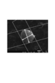
- FIG. 1 is a diagram schematically illustrating an example of a solder particle.
- FIG. 2 is a diagram showing distances X and Y (where Y ⁇ X) between opposing sides when a rectangle circumscribing the projected image of the solder particles is created by two pairs of parallel lines.
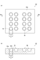
- FIG. 3A is a plan view schematically showing an example of the base
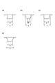
- FIG. 3B is a cross-sectional view taken along the line IIIb-IIIb shown in FIG. 4A to 4D are cross-sectional views schematically showing examples of the cross-sectional shape of the concave portion of the base.
- FIG. 5 is a cross-sectional view schematically showing a state in which the solder fine particles are accommodated in the concave portions of the base.
- FIG. 6 is a cross-sectional view schematically showing a state in which the solder particles are formed in the concave portions of the base.
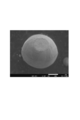
- FIG. 7 is an SEM image of the solder particles obtained in Example 1.
- FIG. 8 is a cross-sectional view schematically showing another example of the cross-sectional shape of the concave portion of the base.
- each component in the composition means the total amount of the plurality of substances present in the composition when there are a plurality of substances corresponding to each component in the composition, unless otherwise specified.
- the numerical range indicated by using “to” indicates a range including the numerical values described before and after “to” as the minimum value and the maximum value, respectively.
- the upper limit or the lower limit of the numerical range of a certain stage may be replaced with the upper limit or the lower limit of the numerical range of another stage.
- the upper limit or the lower limit of the numerical ranges may be replaced with the values shown in the examples.
- solder particles according to the present embodiment have a flat portion on a part of the surface. At this time, it is preferable that the surface other than the flat portion is spherical. That is, the solder particles may have a flat surface portion and a spherical crown-shaped curved surface portion. When an anisotropic conductive material is obtained using such solder particles, it is possible to realize excellent conduction reliability and insulation reliability. Hereinafter, the reason will be described.
- ⁇ Circle over (1) ⁇ By contacting the flat portion of the solder particles with the electrode, a wide contact area can be secured between the flat portion and the electrode. For example, when connecting an electrode formed of a material to which solder easily spreads and an electrode formed of a material to which solder is unlikely to spread, adjustment is performed so that the plane portion of the solder particles is arranged on the latter electrode side. Thereby, connection between both electrodes can be suitably performed.
- the large contact area between the solder particles and the electrodes makes it easier for the solder to spread and spread.
- a method for making the solder particles disposed on the electrode (substrate) wet and spread on the electrode there is a method in which a flux is applied in advance to the solder particles themselves or the electrode, and the solder particles are dissolved by reflow (heating). At this time, when the oxide film of the solder particles is thick, the flux is weak, or the like, if the contact area between the solder particles and the electrode is small, it is difficult for the solder to spread and spread.
- the contact area between the electrode and the solder particles is increased, and the solder particles tend to spread easily. This is because when the oxide film is being removed, if the electrode contacts the surface of the solder particles, the thinned oxide film will crack and the melted solder and flux will flow, removing the oxide film. It is presumed that it is easier to proceed.
- the contact area between the solder particles and the electrode is large, the number of contact points between the electrode and the surface of the solder particle increases, so that the timing of the spread of the wetness becomes early, and the spread of the wettable material becomes easy.
- the solder particles are easily wetted and spread, the amount of flux can be reduced, and the occurrence of ion migration due to the residue of the flux can be suppressed.
- solder particles having the flat portion have good sitting, when the solder particles are arranged on the electrode such that the flat portion and the electrode are in contact with each other, the solder particles are less likely to be displaced due to its stable shape. That is, it is easy to suppress that the solder particles roll out of the space between the electrodes before the reflow, thereby lowering the conduction reliability between the facing electrodes and the insulation reliability between the adjacent electrodes.
- FIG. 1 is a diagram schematically illustrating an example of the solder particles 1 according to the present embodiment.
- the solder particles 1 have a shape in which a flat portion 11 having a diameter A is formed on a part of the surface of a sphere having a diameter B.
- the ratio (A / B) of the diameter A of the flat portion to the diameter B of the solder particles 1 is, for example, more than 0.01 and less than 1.0 (0.01 ⁇ 0.01). (A / B ⁇ 1.0), and may be 0.1 to 0.9.
- the diameter B of the solder particles and the diameter A of the plane portion can be observed by, for example, a scanning electron microscope or the like.
- arbitrary particles are observed with a scanning electron microscope, and an image is taken.
- the diameter B of the solder particles and the diameter A of the plane portion are measured from the obtained image, and the A / B of the particles is determined.
- This operation is performed on 300 solder particles, and an average value is calculated, which is defined as A / B of the solder particles.
- Solder particles 1 have an average particle diameter of 1 to 30 ⁇ m and C.I. V. The value may be 20% or less. Such solder particles have both a small average particle diameter and a narrow particle size distribution, and can be suitably used as conductive particles applied to an anisotropic conductive material having high conductive reliability and insulation reliability.
- the average particle size of the solder particles is not particularly limited as long as it is within the above range, but is preferably 30 ⁇ m or less, more preferably 25 ⁇ m or less, and further preferably 20 ⁇ m or less.
- the average particle size of the solder particles is preferably 1 ⁇ m or more, more preferably 2 ⁇ m or more, and further preferably 4 ⁇ m or more.
- the average particle size of the solder particles can be measured using various methods according to the size. For example, methods such as a dynamic light scattering method, a laser diffraction method, a centrifugal sedimentation method, an electric detection band method, and a resonance mass measurement method can be used. Further, a method of measuring the particle size from an image obtained by an optical microscope, an electron microscope, or the like can be used. Specific examples include a flow-type particle image analyzer, a Microtrac, a Coulter counter, and the like.
- C. of solder particles V The value is preferably 20% or less, more preferably 10% or less, still more preferably 7% or less, and most preferably 5% or less, from the viewpoint of realizing better conductive reliability and insulation reliability.
- the lower limit of the value is not particularly limited.
- C.I. V. The value may be 1% or more, and may be 2% or more.
- the ratio of Y to X may be more than 0.8 and less than 1.0 (0.8 ⁇ Y / X ⁇ 1.0), and may be 0.81 to 0.99.
- Such solder particles can be said to be particles closer to a true sphere.
- solder particles are close to a true sphere, when the plurality of electrodes facing each other are electrically connected via the solder particles, unevenness is hardly generated in the contact between the solder particles and the electrodes, and a stable connection is obtained. Tend. In addition, when a conductive film or paste in which solder particles are dispersed in a resin material is produced, high dispersibility is obtained, and dispersion stability during production tends to be obtained. Furthermore, when a film or paste in which solder particles are dispersed in a resin material is used for connection between electrodes, even if the solder particles rotate in the resin, if the solder particles are spherical, when viewed in a projected image, The projected area of the solder particles is close. Therefore, there is a tendency that stable electric connection with little variation when connecting the electrodes is easily obtained.
- FIG. 2 is a diagram showing distances X and Y (where Y ⁇ X) between opposing sides when a rectangle circumscribing the projected image of the solder particles is created by two pairs of parallel lines.
- a projection image is obtained by observing an arbitrary particle with a scanning electron microscope.
- Y / X of the particle is determined. This operation is performed on 300 solder particles to calculate an average value, which is defined as Y / X of the solder particles.
- the solder particles may include tin or a tin alloy.
- tin alloy for example, In—Sn alloy, In—Sn—Ag alloy, Sn—Au alloy, Sn—Bi alloy, Sn—Bi—Ag alloy, Sn—Ag—Cu alloy, Sn—Cu alloy, etc. are used. be able to. The following examples are given as specific examples of these tin alloys.
- solder particles may include indium or an indium alloy.
- the indium alloy for example, an In—Bi alloy, an In—Ag alloy, or the like can be used. The following examples are given as specific examples of these indium alloys. ⁇ In-Bi (In 66.3% by mass, Bi 33.7% by mass, melting point 72 ° C.) In-Bi (33.0% by mass of In, 67.0% by mass of Bi, melting point 109 ° C.) In-Ag (In 97.0 mass%, Ag 3.0 mass%, melting point 145 ° C)
- tin alloy or indium alloy can be selected according to the use (temperature during use) of the solder particles and the like.
- an In—Sn alloy or a Sn—Bi alloy may be adopted, and in this case, fusion can be performed at 150 ° C. or less.
- a material having a high melting point such as a Sn—Ag—Cu alloy or a Sn—Cu alloy, is employed, high reliability can be maintained even after being left at a high temperature.
- the solder particles may include one or more selected from Ag, Cu, Ni, Bi, Zn, Pd, Pb, Au, P and B.
- Ag or Cu may be contained from the following viewpoints. That is, since the solder particles contain Ag or Cu, the melting point of the solder particles can be reduced to about 220 ° C., and the bonding strength with the electrode is further improved, so that better conduction reliability is obtained. It will be easier.
- the Cu content of the solder particles is, for example, 0.05 to 10% by mass, and may be 0.1 to 5% by mass or 0.2 to 3% by mass.
- the Cu content is 0.05% by mass or more, it is easy to achieve better solder connection reliability.
- solder particles having a low melting point and excellent wettability are likely to be obtained, and as a result, the connection reliability of the joints by the solder particles tends to be good.
- the Ag content of the solder particles is, for example, 0.05 to 10% by mass, and may be 0.1 to 5% by mass or 0.2 to 3% by mass.
- the Ag content is 0.05% by mass or more, it is easy to achieve better solder connection reliability.
- the Ag oil content is 10% by mass or less, solder particles having a low melting point and excellent wettability tend to be obtained, and as a result, the connection reliability of the joints by the solder particles tends to be good.
- solder particles is not particularly limited, and can be suitably used, for example, as conductive particles for an anisotropic conductive material.
- solder particles for electrically connecting electrodes such as a ball grid array connection method (BGA connection) which is widely used for mounting a semiconductor integrated circuit, and for sealing and sealing a component such as a MEMS, brazing, It can also be suitably used for applications such as a spacer for controlling a sheath. That is, the above-mentioned solder particles can be used for general applications in which conventional solder is used.
- BGA connection ball grid array connection method
- the method for producing the solder particles according to the present embodiment is not particularly limited, an example of the production method will be described below.
- the solder particles according to the present embodiment are prepared by preparing a substrate having a plurality of recesses and solder fine particles, storing the solder particles in at least a part of the concave portions of the base, and storing the solder fine particles in the concave portions. A step of fusing the solder fine particles to form solder particles inside the concave portion. According to this manufacturing method, solder particles having a flat portion on a part of the surface are manufactured.
- FIG. 3A is a plan view schematically showing an example of the base 60
- FIG. 3B is a cross-sectional view taken along the line IIIb-IIIb shown in FIG. 3A.
- the base 60 shown in FIG. 3A has a plurality of recesses 62.
- the plurality of recesses 62 may be regularly arranged in a predetermined pattern. In this case, after the solder particles are formed in the concave portion 62, the solder particles in the concave portion 62 are transferred to a resin material or the like, so that the solder particles can be arranged regularly.
- the concave portion 62 of the base 60 is preferably formed in a tapered shape in which the opening area increases from the bottom 62a side of the concave portion 62 toward the surface 60a side of the base 60. That is, as shown in FIG. 3, the width of the bottom 62a of the recess 62 (width a in FIG. 3) is preferably smaller than the width of the opening in the surface 60a of the recess 62 (width b in FIG. 3).
- the size (width a, width b, volume, taper angle, depth, etc.) of the recess 62 may be set according to the size of the target solder particle.
- the shape of the concave portion 62 may be a shape other than the shape shown in FIG.
- the shape of the opening in the surface 60a of the concave portion 62 may be an ellipse, a triangle, a quadrangle, a polygon, or the like, in addition to a circle as shown in FIG.
- the shape of the concave portion 62 in a cross section perpendicular to the surface 60a may be, for example, a shape as shown in FIG.
- FIGS. 4A to 4D are cross-sectional views schematically showing examples of the cross-sectional shape of the concave portion of the base.
- Each of the cross-sectional shapes shown in FIGS. 4A to 4D has a flat bottom surface. Thereby, a flat part is formed on a part of the surface of the solder particle.
- the width (width b) of the opening in the surface 60a of the concave portion 62 is the maximum width in the cross-sectional shape. Thereby, the solder particles formed in the concave portion 62 are easily taken out, and workability is improved.
- the base 60 for example, inorganic materials such as silicon, various ceramics, glass, metals such as stainless steel, and organic materials such as various resins can be used. Among these, it is preferable that the base 60 is made of a material having heat resistance that does not deteriorate at the melting temperature of the solder fine particles. Further, the concave portion 62 of the base 60 can be formed by a known method such as a photolithographic method, an imprint method, a mechanical processing method, an electron beam processing method, a radiation processing method, or the like.
- the solder fine particles prepared in the preparation step may include fine particles having a particle diameter smaller than the width (width b) of the opening in the surface 60a of the concave portion 62, and include more fine particles having a particle diameter smaller than the width b.
- the solder fine particles preferably have a particle size distribution D10 particle size smaller than width b, more preferably a particle size distribution D30 particle size smaller than width b, and a particle size distribution D50 particle size smaller than width b. More preferred.
- the particle size distribution of the solder particles can be measured using various methods according to the size. For example, methods such as a dynamic light scattering method, a laser diffraction method, a centrifugal sedimentation method, an electric detection band method, and a resonance mass measurement method can be used. Further, a method of measuring the particle size from an image obtained by an optical microscope, an electron microscope, or the like can be used. Specific examples include a flow-type particle image analyzer, a Microtrac, a Coulter counter, and the like.
- C C. of the solder fine particles prepared in the preparation process V The value is not particularly limited, but from the viewpoint of improving the filling property of the concave portion 62 by a combination of large and small fine particles, C.I. V.
- the value is preferably high.
- the value may be higher than 20%, preferably higher than 25%, more preferably higher than 30%.
- Solder fine particles C.I. V. The value is calculated by multiplying the value obtained by dividing the standard deviation of the particle size measured by the above-described method by the average particle size (D50 particle size) by 100.
- the solder particles may include tin or a tin alloy.
- tin alloy for example, In—Sn alloy, In—Sn—Ag alloy, Sn—Au alloy, Sn—Bi alloy, Sn—Bi—Ag alloy, Sn—Ag—Cu alloy, Sn—Cu alloy, etc. are used. be able to. The following examples are given as specific examples of these tin alloys.
- solder particles may include indium or an indium alloy.
- the indium alloy for example, an In—Bi alloy, an In—Ag alloy, or the like can be used. The following examples are given as specific examples of these indium alloys. ⁇ In-Bi (In 66.3% by mass, Bi 33.7% by mass, melting point 72 ° C.) In-Bi (33.0% by mass of In, 67.0% by mass of Bi, melting point 109 ° C.) In-Ag (In 97.0 mass%, Ag 3.0 mass%, melting point 145 ° C)
- the above-mentioned tin alloy or indium alloy can be selected according to the use (temperature during use) of the solder particles and the like. For example, when it is desired to obtain solder particles used for fusion at a low temperature, an In—Sn alloy or a Sn—Bi alloy may be adopted. In this case, solder particles that can be fused at 150 ° C. or lower are obtained. When a material having a high melting point, such as a Sn—Ag—Cu alloy or a Sn—Cu alloy, is used, solder particles that can maintain high reliability even after being left at a high temperature can be obtained.
- a material having a high melting point such as a Sn—Ag—Cu alloy or a Sn—Cu alloy
- the solder fine particles may include one or more selected from Ag, Cu, Ni, Bi, Zn, Pd, Pb, Au, P and B.
- Ag or Cu may be contained from the following viewpoints. That is, since the solder fine particles contain Ag or Cu, the melting point of the obtained solder particles can be reduced to about 220 ° C., and the solder particles having excellent bonding strength with the electrode can be obtained, so that good conduction reliability can be obtained. Is obtained.
- the Cu content of the solder fine particles is, for example, 0.05 to 10% by mass, and may be 0.1 to 5% by mass or 0.2 to 3% by mass.
- the Cu content is 0.05% by mass or more, it becomes easy to obtain solder particles capable of achieving good solder connection reliability.
- the Cu content is 10% by mass or less, solder particles having a low melting point and excellent wettability are easily obtained, and as a result, the connection reliability of the joints by the solder particles is easily improved.
- the Ag content of the solder particles is, for example, 0.05 to 10% by mass, and may be 0.1 to 5% by mass or 0.2 to 3% by mass.
- the Ag content is 0.05% by mass or more, solder particles that can achieve good solder connection reliability are easily obtained.
- the Ag oil content is 10% by mass or less, solder particles having a low melting point and excellent wettability are easily obtained, and as a result, the connection reliability of the joints by the solder particles is easily improved.
- the solder fine particles prepared in the preparation step are accommodated in each of the recesses 62 of the base 60.
- the accommodating step may be a step of accommodating all of the solder fine particles prepared in the preparing step in the concave portion 62, and a part of the solder fine particles prepared in the preparing step (for example, the width b of the opening of the concave portion 62 among the solder fine particles). (Smaller one) in the recess 62.
- FIG. 5 is a cross-sectional view schematically showing a state in which the solder fine particles 111 are accommodated in the concave portions 62 of the base 60. As shown in FIG. 5, a plurality of solder particles 111 are accommodated in each of the plurality of recesses 62.
- the amount of the solder fine particles 111 accommodated in the concave portion 62 is, for example, preferably 20% or more, more preferably 30% or more, even more preferably 50% or more based on the volume of the concave portion 62. , 60% or more. Thereby, the variation in the accommodation amount is suppressed, and solder particles having a smaller particle size distribution are easily obtained.
- the method for accommodating the solder fine particles in the concave portion 62 is not particularly limited.
- the storage method may be either a dry method or a wet method.
- the solder fine particles prepared in the preparation step on the base 60 and rubbing the surface 60a of the base 60 with a squeegee, sufficient solder fines are accommodated in the recess 62 while removing excess solder fines. can do.
- the width b of the opening of the concave portion 62 is larger than the depth of the concave portion 62, the solder fine particles may jump out of the opening of the concave portion 62.
- a squeegee is used, the solder particles protruding from the opening of the concave portion 62 are removed.
- Examples of a method for removing excess solder fine particles include a method of blowing compressed air, a method of rubbing the surface 60a of the base 60 with a nonwoven fabric or a bundle of fibers, and the like. These methods are preferable in handling solder particles that are easily deformed because the physical force is weaker than that of a squeegee. Further, in these methods, the solder fine particles protruding from the opening of the concave portion 62 can be left in the concave portion.
- the fusion step is a step of fusing the solder particles 111 housed in the concave portions 62 to form the solder particles 1 inside the concave portions 62.
- FIG. 6 is a cross-sectional view schematically showing a state in which the solder particles 1 are formed in the concave portions 62 of the base 60.
- the solder fine particles 111 accommodated in the concave portion 62 are united by melting and are sphericalized by surface tension.
- the molten solder follows the bottom portion 62a to form the flat portion 11.
- the formed solder particles 1 have a shape having the flat portion 11 on a part of the surface.
- FIG. 1 is a view of the solder particles 1 viewed from the side opposite to the opening of the recess 62 in FIG.
- solder fine particles 111 As a method of melting the solder fine particles 111 accommodated in the concave portion 62, there is a method of heating the solder fine particles 111 to a temperature equal to or higher than the melting point of the solder. Due to the effect of the oxide film, the solder fine particles 111 may not melt even when heated at a temperature higher than the melting point, may not spread, or may not coalesce. For this reason, the solder fine particles 111 are exposed to a reducing atmosphere, the surface oxide film of the solder fine particles 111 is removed, and then the solder fine particles 111 are heated to a temperature equal to or higher than the melting point of the solder fine particles 111, so that the solder fine particles 111 are melted and spread. Can be unified.
- the melting of the solder fine particles 111 is preferably performed in a reducing atmosphere.
- a reducing atmosphere By heating the solder fine particles 111 to a temperature higher than the melting point of the solder fine particles 111 and in a reducing atmosphere, the oxide film on the surface of the solder fine particles 111 is reduced, so that the solder fine particles 111 are melted, spread, and united efficiently. It becomes easier to progress.
- the method for setting the reducing atmosphere is not particularly limited as long as the above-described effects can be obtained.
- the solder fine particles 111 can be melted in a reducing atmosphere.
- These devices may include a heating device, a chamber for filling an inert gas (nitrogen, argon, etc.) in the furnace, a mechanism for evacuating the chamber, and the like, which makes it easier to control the reducing gas.
- voids can be removed by decompression after melting and coalescence of the solder fine particles 111, and the solder particles 1 with more excellent connection stability can be obtained.
- the profile of the solder fine particles 111 such as reduction, melting conditions, temperature, and atmosphere adjustment in the furnace may be appropriately set in consideration of the melting point, the particle size, the size of the concave portion, the material of the base 60, and the like.
- the substrate 60 having the recesses filled with the solder fine particles 111 is inserted into a furnace, and after evacuation, a reducing gas is introduced to fill the furnace with the reducing gas, and the surface oxide film of the solder fine particles 111 is formed. After the removal, the reducing gas is removed by vacuuming, and then heated to the melting point of the solder fine particles 111 or more to dissolve and coalesce the solder fine particles, and form the solder particles in the concave portion 62.
- solder particles 1 After filling with nitrogen gas, the temperature in the furnace is returned to room temperature, and solder particles 1 can be obtained. Also, for example, after inserting the substrate 60 in which the solder fine particles 111 are filled in the recesses into the furnace and performing evacuation, a reducing gas is introduced, the inside of the furnace is filled with the reducing gas, and the furnace heater is used. After heating the solder fine particles 111 to remove the surface oxide film of the solder fine particles 111, the reducing gas is removed by evacuation, and then heated to the melting point of the solder fine particles 111 or more to dissolve and unite the solder fine particles.
- the temperature in the furnace is returned to room temperature after filling with nitrogen gas, and the solder particles 1 can be obtained.
- the reducing power is increased and the oxide film on the surface of the solder fine particles is easily removed.
- the furnace heater is used.
- the substrate 60 is heated to a temperature equal to or higher than the melting point of the solder fine particles 111 to remove the surface oxide film of the solder fine particles 111 by reduction, and at the same time, dissolve and coalesce the solder fine particles.
- the furnace temperature is returned to room temperature after filling with nitrogen gas, and the solder particles 1 can be obtained.
- the treatment can be performed in a short time because the rise and fall of the furnace temperature need only be adjusted once.
- a step of removing the surface oxide film that has not been completely removed by again setting the inside of the furnace to a reducing atmosphere is performed. Residue such as a part of the oxide film remaining on the substrate can be reduced.
- the substrate 60 filled with the solder fine particles 111 in the concave portion is placed on a conveyor for conveyance, and continuously passed through a plurality of zones to obtain the solder particles 1.
- the substrate 60 in which the recesses are filled with the solder fine particles 111 is placed on a conveyor set at a constant speed, and passed through a zone filled with an inert gas such as nitrogen or argon at a temperature lower than the melting point of the solder fine particles 111, Subsequently, the powder is passed through a zone in which a reducing gas such as formic acid gas at a temperature lower than the melting point of the solder fine particles 111 is present to remove the surface oxide film of the solder fine particles 111.
- solder particles 111 are melted and coalesced by passing through a zone filled with an inert gas such as argon, and then passed through a cooling zone filled with an inert gas such as nitrogen or argon to obtain solder particles 1. be able to.
- an inert gas such as argon
- the substrate 60 in which the recesses are filled with the solder particles 111 is placed on a conveyor set at a constant speed, and passed through a zone filled with an inert gas such as nitrogen or argon at a temperature equal to or higher than the melting point of the solder particles 111, Subsequently, it is passed through a zone in which a reducing gas such as formic acid gas at a temperature equal to or higher than the melting point of the solder fine particles 111 is present to remove the surface oxide film of the solder fine particles 111, melt and coalesce. Through the cooling zone filled with the inert gas, the solder particles 1 can be obtained.
- an inert gas such as nitrogen or argon
- the conveyor furnace can process at atmospheric pressure, it is also possible to continuously process a film-like material by roll-to-roll.
- a continuous roll product of the substrate 60 in which the recesses are filled with the solder fine particles 111 is prepared, a roll unwinder is installed at the entrance side of the conveyor furnace, and a roll take-up machine is installed at the exit side of the conveyor furnace.
- the solder fine particles 111 filled in the concave portions can be fused.
- the formed solder particles 1 may be transported or stored while being accommodated in the concave portion 62 of the base 60, or may be removed from the concave portion 62 and collected.
- a resin material may be disposed on the surface 60a of the base 60, and the solder particles 1 in the concave portion 62 may be transferred to the resin material.
- the solder particles 1 can be regularly arranged on the resin material.
- the plane portion of the arranged solder particles 1 can be maintained in one direction. For this reason, the flat portion is effectively used at the time of electrode connection, and as described above, advantages such as securing a large contact area between the solder particles and the electrode and suppressing displacement of the solder particles are easily enjoyed.
- uniform size solder particles can be formed regardless of the material and shape of the solder fine particles.
- indium-based solder can be deposited by plating, but it is difficult to deposit in the form of particles, and it is soft and difficult to handle.
- indium-based solder particles having a uniform particle diameter can be easily manufactured by using indium-based solder fine particles as a raw material.
- the formed solder particles 1 can be handled in a state of being accommodated in the concave portion 62 of the base 60, the solder particles can be transported and stored without deforming the solder particles.
- the formed solder particles 1 are simply housed in the concave portions 62 of the base body 60, they can be easily taken out and can be collected and surface-treated without deforming the solder particles.
- the solder fine particles 111 may have a large variation in the particle size distribution or may have a distorted shape. If the solder fine particles 111 can be accommodated in the concave portion 62, they can be used as a raw material in the manufacturing method of the present embodiment.
- the shape of the concave portion 62 of the base 60 can be freely designed by a lithography method, an imprint method, an electron beam processing method, a radiation processing method, a machining method, or the like. Since the size of the solder particles 1 depends on the amount of the solder fine particles 111 accommodated in the concave portions 62, the size of the solder particles 1 can be freely designed by designing the concave portions 62 in the manufacturing method of the present embodiment.
- Step a1 Classification of solder fine particles
- 100 g of Sn-Bi solder fine particles manufactured by 5N Plus, melting point: 139 ° C., Type 8
- 5N Plus melting point: 139 ° C.
- Type 8 melting point: 139 ° C.
- This operation was repeated to collect 10 g of the solder fine particles.
- the average particle diameter of the obtained solder fine particles was 1.0 ⁇ m, and C.I. V. The value was 42%.
- Step b1 disposition on substrate
- Polyimide film, thickness 100 ⁇ m was prepared.
- the plurality of recesses were regularly arranged at intervals of 1.0 ⁇ m.
- the solder fine particles (average particle diameter: 1.0 ⁇ m, CV value: 42%) obtained in step a) were arranged in the concave portions of the base.
- Step c1 formation of solder particles
- the substrate having the solder fine particles disposed in the recesses in the step b1 was placed in a hydrogen reduction furnace, and after evacuation, hydrogen gas was introduced into the furnace to fill the furnace with hydrogen. Thereafter, the inside of the furnace was maintained at 280 ° C. for 20 minutes, and then vacuum was applied again, nitrogen was introduced, the pressure was returned to the atmospheric pressure, and the temperature in the furnace was lowered to room temperature to form solder particles.
- solder particles were collected from the concave portion by tapping the substrate after step c1 from the back side of the concave portion.
- the obtained solder particles were observed by the following method.
- the obtained solder particles are placed on a conductive tape fixed to the surface of a scanning electron microscope (SEM) observation pedestal, and the SEM observation pedestal is tapped on a 5-mm-thick stainless steel plate so that the solder particles are all over the conductive tape. Spread out evenly. Thereafter, a compressed nitrogen gas was blown onto the surface of the conductive tape to fix the solder particles on the conductive tape in a single layer.
- FIG. 7 shows the observation results.
- FIG. 7 is an SEM image of the solder particles obtained in Example 1. As shown in the figure, the obtained solder particles had a shape in which a flat portion was formed on a part of the surface of the sphere. Note that the solder particles obtained in the other examples also had the same shape.
- Step c2 Formation of Solder Particles
- the substrate having the solder fine particles arranged in the recesses in step b1 is put into a hydrogen radical reduction furnace (plasma reflow device manufactured by Shinko Seiki Co., Ltd.), and after evacuation, hydrogen gas is introduced into the furnace. After the introduction, the inside of the furnace was filled with hydrogen gas. Then, the inside of the furnace was adjusted to 120 ° C., and irradiated with hydrogen radicals for 5 minutes. After that, hydrogen gas in the furnace was removed by evacuation, heated to 170 ° C., nitrogen was introduced into the furnace to return to atmospheric pressure, and then the temperature in the furnace was lowered to room temperature to reduce the solder particles. Formed.
- a hydrogen radical reduction furnace plasma reflow device manufactured by Shinko Seiki Co., Ltd.
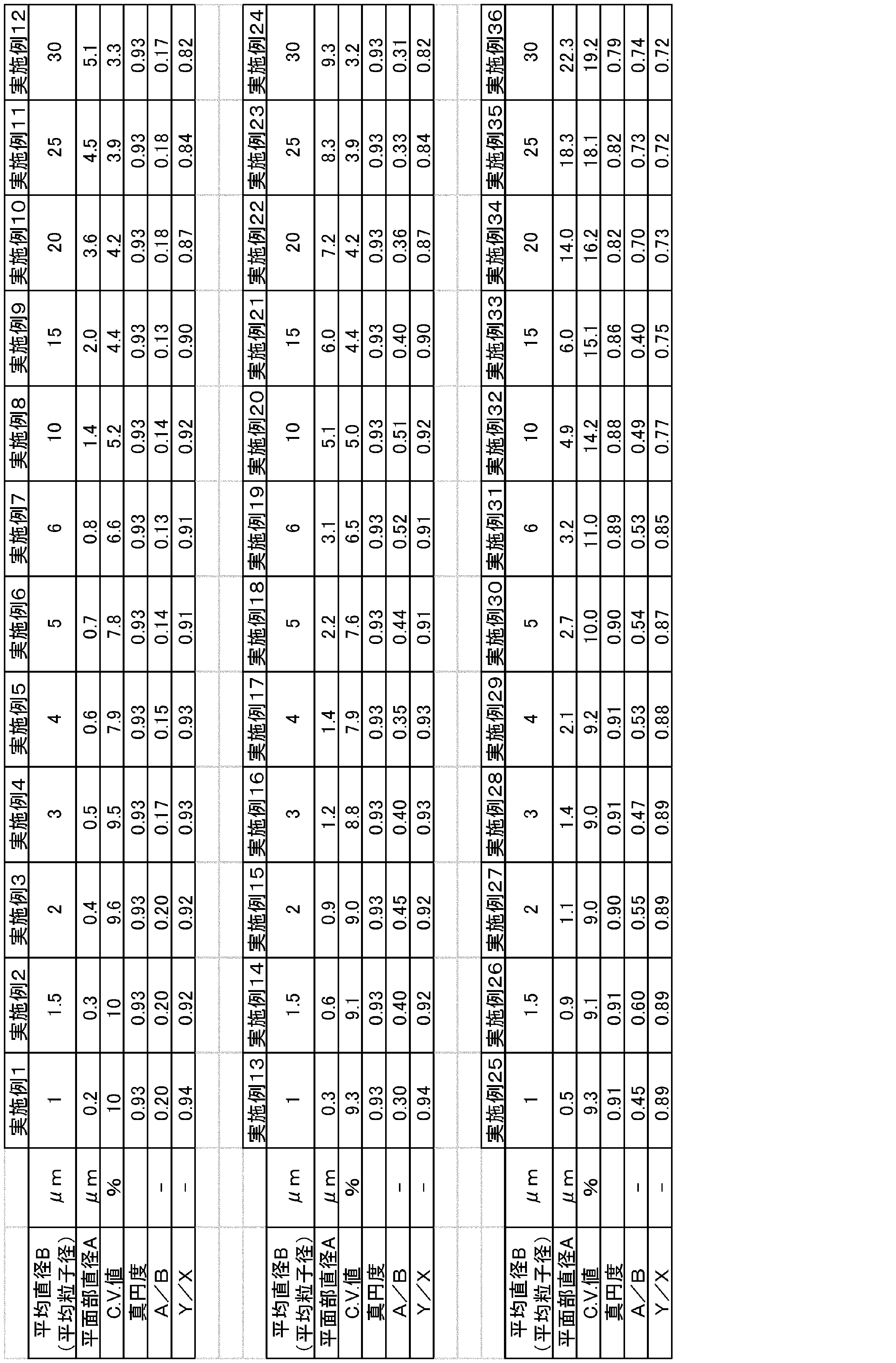
- Example 14 to 24 Except that the size of the concave portion was changed as described in Table 1, solder particles were prepared, collected, and evaluated in the same manner as in Example 13. Table 2 shows the results.
- Step c2 Formation of Solder Particles
- the substrate having the solder fine particles arranged in the recesses in step b1 is put into a hydrogen radical reduction furnace (plasma reflow device manufactured by Shinko Seiki Co., Ltd.), and after evacuation, hydrogen gas is introduced into the furnace. After the introduction, the inside of the furnace was filled with hydrogen gas. Then, the inside of the furnace was adjusted to 120 ° C., and irradiated with hydrogen radicals for 5 minutes. Then, the hydrogen gas in the furnace was removed by evacuation, heated to 145 ° C., nitrogen was introduced into the furnace to return to atmospheric pressure, and then the temperature in the furnace was lowered to room temperature to reduce the solder particles. Formed.
- a hydrogen radical reduction furnace plasma reflow device manufactured by Shinko Seiki Co., Ltd.
- Example 26 to 36 Except that the size of the concave portion was changed as described in Table 1, solder particles were prepared, collected, and evaluated in the same manner as in Example 25. Table 2 shows the results.
- Step d1 Flux filling into recess
- a coating solution was prepared by dissolving 10 g of adipic acid in 200 g of toluene, and this was applied to a substrate (transfer type) in which the solder particles were arranged in the recesses in step c1. Then, an excess coating solution was removed using a squeegee, and the inside of the concave portion was filled with the coating solution. This was charged into an explosion-proof dryer at 80 ° C. for 1 minute to vaporize toluene, so that a concave portion was filled with adipic acid as a flux component.
- Step e1 Preparation of adhesive film
- Copolymer of 100 g of phenoxy resin (manufactured by Union Carbide, trade name "PKHC”) and acrylic rubber 40 parts by mass of butyl acrylate, 30 parts by mass of ethyl acrylate, 30 parts by mass of acrylonitrile, 3 parts by mass of glycidyl methacrylate, molecular weight: 85 75 g
- PKHC phenoxy resin
- acrylic rubber 40 parts by mass of butyl acrylate, 30 parts by mass of ethyl acrylate, 30 parts by mass of acrylonitrile, 3 parts by mass of glycidyl methacrylate, molecular weight: 85 75 g
- a liquid epoxy resin containing a microcapsule-type latent curing agent (epoxy equivalent: 185, manufactured by Asahi Kasei Epoxy Co., Ltd., trade name “NOVACURE HX-3941”) was added, and stirred to obtain an adhesive solution.
- the obtained adhesive solution was applied to a separator (silicone-treated polyethylene terephthalate film, thickness: 40 ⁇ m) using a roll coater, and dried by heating at 90 ° C. for 10 minutes to obtain a thickness of 4, 6, 8, 12, and 20 ⁇ m adhesive films (insulating resin films) were prepared on the separator.
- Step f1 Transfer of solder particles
- Step g1 Preparation of anisotropic conductive film
- the transfer surface of the adhesive film obtained in step f1 is brought into contact with the adhesive film produced in the same manner as in step e1, and heated and pressed at 50 ° C. and 0.1 MPa (1 kgf / cm 2 ) to obtain a film.
- an anisotropic conductive film was obtained in which the solder particles were arranged in a layered manner and the plane part of the solder particles was opposed to only one of the main surfaces of the film.
- 4 ⁇ m is superimposed on a film having a thickness of 4 ⁇ m
- 6 ⁇ m for 6 ⁇ m, 8 ⁇ m for 8 ⁇ m, 12 ⁇ m for 12 ⁇ m, and 20 ⁇ m for 20 ⁇ m are superimposed to form 8 ⁇ m, 12 ⁇ m, 16 ⁇ m
- Anisotropic conductive films having a thickness of 24 ⁇ m and 40 ⁇ m were prepared.
- the adhesive film obtained in the step f1 was cut out at a size of 10 cm ⁇ 10 cm, Pt sputtering was performed on the surface on which the solder particles were arranged, and then SEM observation was performed. After observing 300 solder particles, the average diameter B (average particle diameter) of the solder particles, the average diameter A of the plane portion, and C. V. Values, roundness, A / B and Y / X were calculated. Table 2 shows the results. Roundness: the ratio r / R of the radii of two concentric circles (the radius r of the minimum circumscribed circle and the radius R of the maximum inscribed circle) of the solder particles.
- a / B The ratio of the diameter A of the flat portion to the diameter B of the solder particles.
- Y / X When a rectangle circumscribing the projected image of the solder particles is created by two pairs of parallel lines, the distance between opposing sides is defined as X and Y (where Y ⁇ X). ratio.
- Step h1 Preparation of Chip with Copper Bump
- Chip C1 area 30 ⁇ m ⁇ 30 ⁇ m, space 30 ⁇ m, height: 10 ⁇ m
- number of bumps 362 Chip C2 area 15 ⁇ m ⁇ 15 ⁇ m, space 10 ⁇ m, height: 10 ⁇ m
- number of bumps 362 Chip C3 area 10 ⁇ m ⁇ 10 ⁇ m, space 10 ⁇ m, height: 7 ⁇ m
- number of bumps 362 Chip C4 area 5 ⁇ m ⁇ 5 ⁇ m, space 6 ⁇ m, height: 5 ⁇ m
- number of bumps 362 Chip C5 area 3 ⁇ m ⁇ 3 ⁇ m, space 3 ⁇ m, height: 5 ⁇ m, number of bumps 362
- Step i1 Preparation of Substrate with Copper Bump
- Substrate D1 Area 30 ⁇ m ⁇ 30 ⁇ m, space 30 ⁇ m, height: 10 ⁇ m, number of bumps 362 ⁇
- Substrate D2 Area 15 ⁇ m ⁇ 15 ⁇ m, space 10 ⁇ m, height: 10 ⁇ m, number of bumps 362 ⁇
- Substrate D3 Area 10 ⁇ m ⁇ 10 ⁇ m, space 10 ⁇ m, height: 7 ⁇ m, number of bumps 362 ⁇
- Substrate D4 area 5 ⁇ m ⁇ 5 ⁇ m, space 6 ⁇ m, height 5 ⁇ m, number of bumps 362 ⁇
- Substrate D5 area 3 ⁇ m ⁇ 3 ⁇ m, space 3 ⁇ m, height: 5 ⁇ m, number of bumps 362 (Step j1: connection of a chip with copper bumps and a substrate with copper bumps)
- Step j1 connection of a chip with copper bumps and a substrate with copper bumps
- Heating and pressurizing were performed from above the chip under the conditions of 180 ° C., 40 gf / bump, and 30 seconds, and the main connection was performed.
- a total of seven types of connection structures according to (1) to (7) were produced by combining the following “chip / anisotropic conductive film / substrate” of (1) to (7).
- Chip C1 / 40 ⁇ m thick conductive film / substrate D1 (2) Conductive film / substrate D1 with chip C 1/24 ⁇ m thick (3) Chip C1 / 16 ⁇ m thick conductive film / substrate D1 (4) Chip C2 / conductive film / substrate D2 having a thickness of 16 ⁇ m (5) Chip C3 / 12 conductive film / substrate D3 having a thickness of 12 ⁇ m (6) Chip C4 / 8 ⁇ m thick conductive film / substrate D4 (7) Chip C5 / 8 ⁇ m thick conductive film / substrate D5
- the above polymer was prepared as follows. Synthesis of reaction product (polymer A) of bisphenol F with 1,6-hexanediol diglycidyl ether and bisphenol F type epoxy resin: 72 parts by mass of bisphenol F (containing 4,4'-methylenebisphenol, 2,4'-methylenebisphenol and 2,2'-methylenebisphenol at a mass ratio of 2: 3: 1), 1,6-hexanediol 70 parts by mass of glycidyl ether and 30 parts by mass of a bisphenol F type epoxy resin ("EPICLON EXA-830CRP" manufactured by DIC Corporation) were placed in a three-necked flask, and dissolved at 150 ° C. under a nitrogen flow.
- thermosetting compound a resorcinol type epoxy compound, “EX-201” manufactured by Nagase ChemteX Corporation was used.
- Pentaerythritol tetrakis (3-mercaptobutyrate) was used as the high dielectric constant curing agent.
- the flux coated solder particles were prepared as follows. 200 g of SnBi solder particles (“ST-3” manufactured by Mitsui Kinzoku Co., Ltd.), 40 g of adipic acid and 70 g of acetone were weighed in a three-necked flask, and then hydroxyl groups on the surface of the solder particle body and carboxyl groups of adipic acid were measured. Then, 0.3 g of dibutyltin oxide, which is a dehydration-condensation catalyst, was added thereto and reacted at 60 ° C. for 4 hours. Thereafter, the solder particles were collected by filtration.
- the collected solder particles, 50 g of adipic acid, 200 g of toluene, and 0.3 g of p-toluenesulfonic acid were weighed in a three-necked flask, and reacted at 120 ° C. for 3 hours while evacuating and refluxing. . At this time, the reaction was carried out using a Dean-Stark extraction device while removing water generated by dehydration condensation. Thereafter, the solder particles were collected by filtration, washed with hexane, and dried. Then, after the obtained solder particles were crushed by a ball mill, a sieve was selected so as to have a predetermined CV value. The average particle size of the obtained SnBi solder particles (flux-coated solder particles) was 4 ⁇ m, and the CV value was 31%.
- solder particle-containing anisotropic conductive paste a chip with a copper bump and a substrate with a copper bump were connected in the same manner as in Production Example 1 to produce a connection structure.
- An anisotropic conductive paste containing solder particles was applied to the upper part of the substrate, and a chip was mounted thereon.
- the bumps on the chip with copper bumps were aligned with the bumps on the substrate with copper bumps, and heating and pressurization were performed from above the chip under the conditions of 180 ° C., 4 gf / bump, and 30 seconds, to make the actual connection.
- connection structure> A conduction resistance test and an insulation resistance test were performed on a part of the obtained connection structure as follows.
- solder connection reliability was evaluated to be good when the following criteria A or B were satisfied after 20 drops.
- the insulation resistance test Regarding the insulation resistance between the chip electrodes, the initial value of the insulation resistance and the value after the migration test (temperature of 60 ° C., humidity of 90%, and applied for 20 hours at 100 V, 500 hours, and 1000 hours) were measured for 20 samples. The proportion of the samples having an insulation resistance value of 10 9 ⁇ or more in all 20 samples was calculated. The insulation resistance was evaluated from the obtained ratio according to the following criteria. Table 5 shows the results. In addition, when the criteria of the following A or B are satisfied after 1000 hours of the moisture absorption heat test, it can be said that the insulation resistance is good. A: The ratio of the insulation resistance value of 10 9 ⁇ or more is 100%.
- Ratio of insulation resistance value of 10 9 ⁇ or more is 90% or more and less than 100%
- C Ratio of insulation resistance value of 10 9 ⁇ or more is 80% or more and less than 90%
- D Ratio of insulation resistance value of 10 9 ⁇ or more is 50% Not less than 80%
- E the ratio of the insulation resistance value of 10 9 ⁇ or more is less than 50%
- step b1 the sectional shape shown in FIG. 8 (the approximate concave shape as in FIG. 4B), that is, the bottom diameter a is 0.6 ⁇ m, the opening diameter b1 is 1.0 ⁇ m, and the opening diameter b2 is 1.2 ⁇ m (bottom diameter a : 1.0 ⁇ m ⁇ , when the opening is viewed from the upper surface, the opening b2 is located at the center of 1.2 ⁇ m ⁇ ).
- the bottom diameter a 0.6 ⁇ m
- the opening diameter b1 is 1.0 ⁇ m
- the opening diameter b2 is 1.2 ⁇ m (bottom diameter a : 1.0 ⁇ m ⁇ , when the opening is viewed from the upper surface, the opening b2 is located at the center of 1.2 ⁇ m ⁇ ).
- Examples 49 to 51> 10 g of Sn-Bi solder fine particles (manufactured by 5N Plus, melting point: 139 ° C., Type 9), average particle diameter: 3.0 ⁇ m, C.I. V. A solder particle was produced, collected and evaluated in the same manner as in Example 13, except that the value was 32% and that the recesses shown in Table 14 were used in Step b1. Table 15 shows the results.
- step a1 10 g of Sn—Bi solder fine particles (manufactured by 5N Plus, melting point: 139 ° C., Type 10), average particle diameter: 2.8 ⁇ m, C.I. V.
- a solder particle was prepared, collected and evaluated in the same manner as in Example 13 except that the value was 28% and that the recesses shown in Table 14 were used in Step b1. Table 15 shows the results.
- step a1 100 g of In-Sn solder fine particles (manufactured by 5N Plus, melting point: 120 ° C., Type 8) are immersed in distilled water, ultrasonically dispersed, and allowed to stand, and the fine solder particles floating in the supernatant are collected. And an average particle diameter of 1.0 ⁇ m, C.I. V. Example 13 was repeated except that the solder fine particles having a value of 40% were used, the recesses shown in Table 14 were used in the step b1, and the following step c2 was performed instead of the step c1. Then, solder particles were prepared, collected, and evaluated. Table 15 shows the results.
- Step c2 Formation of Solder Particles
- the substrate having the solder fine particles arranged in the recesses in step b1 is put into a hydrogen radical reduction furnace (plasma reflow device manufactured by Shinko Seiki Co., Ltd.), and after evacuation, hydrogen gas is introduced into the furnace. After the introduction, the inside of the furnace was filled with hydrogen gas. Then, the inside of the furnace was adjusted to 110 ° C., and irradiated with hydrogen radicals for 5 minutes. Thereafter, the hydrogen gas in the furnace was removed by evacuation, heated to 160 ° C., nitrogen was introduced into the furnace to return to atmospheric pressure, and then the temperature in the furnace was lowered to room temperature to reduce the solder particles. Formed.
- a hydrogen radical reduction furnace plasma reflow device manufactured by Shinko Seiki Co., Ltd.
- step a1 100 g of Sn—Ag—Cu solder fine particles (manufactured by 5N Plus, melting point: 219 ° C., Type 8) are immersed in distilled water, ultrasonically dispersed, and then allowed to stand. Collected, average particle size 1.0 ⁇ m, C.I. V. Example 13 was repeated except that the solder fine particles having a value of 41% were used, the recesses shown in Table 14 were used in step b1, and the following step c2 was performed instead of step c1. Then, solder particles were prepared, collected, and evaluated. Table 15 shows the results.
- Step c2 Formation of Solder Particles
- the substrate having the solder fine particles arranged in the recesses in step b1 is put into a hydrogen radical reduction furnace (plasma reflow device manufactured by Shinko Seiki Co., Ltd.), and after evacuation, hydrogen gas is introduced into the furnace. After the introduction, the inside of the furnace was filled with hydrogen gas. Thereafter, the inside of the furnace was adjusted to 150 ° C., and irradiated with hydrogen radicals for 3 minutes. Then, the hydrogen gas in the furnace was removed by evacuation, and after heating to 240 ° C., nitrogen was introduced into the furnace to return to the atmospheric pressure, and then the temperature in the furnace was lowered to room temperature to reduce the solder particles. Formed.
- a hydrogen radical reduction furnace plasma reflow device manufactured by Shinko Seiki Co., Ltd.
- the method of the present invention can produce solder particles having a uniform particle size.
- the CV value of the solder particles obtained after reduction and melting tends to be lower when the size of the concave portion is smaller (for example, the bottom portion is 2 ⁇ m or 3 ⁇ m). This is presumably because the smaller the center particle diameter of the solder fine particles, the higher the filling rate in the concave portions and the smaller the variation in filling among the plurality of concave portions.
- solder particles having a uniform particle diameter and different melting points can be easily obtained only by changing the composition of the solder fine particles. Also, various cross-sectional shapes of the concave portion can be used.
- the cross-sectional shape of the concave portion can be appropriately selected according to the final use method and form of the solder particles.
- the surface of the solder particles preferably has a continuous curved surface.
- the solder particles are dispersed in the film and the solder particles are brought into contact with the electrodes by the pressure bonding process, depending on the shape and material of the electrodes, if the solder particles have a flat portion, the impact on the electrodes at the time of contact is reduced, Electrode damage can be prevented.
- the resin whose viscosity has been reduced due to heating in the pressure bonding process may flow and move from above the electrode, but if the resin has a flat portion, the contact area with the electrode is likely to be large, so that when the oxide film is removed by the flux, Since the wetting of the electrodes is widened, there is also an advantage that movement due to resin flow can be suppressed. A similar phenomenon is observed in the resin paste. Furthermore, after transferring the solder particles having a flat portion partially to the adhesive resin film obtained in the preparation example of the present application, or pouring the adhesive resin into the substrate to form a film, and removing the substrate, the solder particles are formed in the film. Can be aligned in substantially the same direction.
- the electrodes When the electrodes are pressure-bonded to each other using such an adhesive resin film containing solder particles, the electrodes made of a very thin or weak material come into contact with the flat surface, thereby suppressing electrode damage. I can do it. Further, even for an electrode that is difficult to wet and spread, the flat portion comes into contact with the surface at the time of pressure bonding, so that there is an advantage that wet spread is more likely to occur due to removal of the oxide film of the solder particles than point contact with a spherical surface.
- the electrodes to be connected generally have different configurations and materials, and as in the present application, the feature that the orientation of the flat portion of the solder particles and the like can be generally aligned is that an adhesive resin is used in accordance with the electrode material. There is a feature that more reliable connection can be realized by selecting the film arrangement position.
- solder particles obtained in Examples 46, 47, and 48 were placed on Au electrodes of 10 ⁇ m, 20 ⁇ m, and 50 ⁇ m formed by sputtering through masks having openings of 6 ⁇ m, 14 ⁇ m, and 40 ⁇ m, respectively.
- the substrate on which the Au electrode was formed was tilted at 15, 20, 30, or 45 degrees, and vibration was applied by hitting with a metal spatula. After the vibration was applied, the surface of the electrode was observed. As a result, the solder particles remaining on the electrode were particles whose flat portions were in contact with the Au electrode surface.
- solder particles are arranged on the electrode as in the process of BGA connection or the like, there is a feature that it is difficult to move from the electrode due to the influence of vibration or wind due to the presence of the flat portion.
- solder particles 11: flat portion, 111: solder fine particles, 60: base, 60a: surface, 62: concave portion, 62a: bottom.
Landscapes
- Engineering & Computer Science (AREA)
- Chemical & Material Sciences (AREA)
- Mechanical Engineering (AREA)
- Materials Engineering (AREA)
- Organic Chemistry (AREA)
- Metallurgy (AREA)
- Spectroscopy & Molecular Physics (AREA)
- Microelectronics & Electronic Packaging (AREA)
- Manufacturing & Machinery (AREA)
- Physics & Mathematics (AREA)
- Dispersion Chemistry (AREA)
- Electric Connection Of Electric Components To Printed Circuits (AREA)
- Powder Metallurgy (AREA)
- Conductive Materials (AREA)
Abstract
Description
0.01<A/B<1.0
0.8<Y/X<1.0
本実施形態に係るはんだ粒子は、表面の一部に平面部を有する。このとき当該平面部以外の表面は、球冠状であることが好ましい。すなわち、はんだ粒子は、平面部と、球冠状の曲面部と、を有するものであってよい。このようなはんだ粒子を用いて異方性導電材料を得た場合、優れた導通信頼性及び絶縁信頼性を実現することが可能である。以下、この理由について説明する。
具体的には、任意の粒子を走査型電子顕微鏡により観察し、画像を撮影する。得られた画像からはんだ粒子の直径B及び平面部の直径Aを測定し、その粒子のA/Bを求める。この作業を300個のはんだ粒子に対して行って平均値を算出し、はんだ粒子のA/Bとする。
例えば、はんだ粒子のC.V.値は1%以上であってよく、2%以上であってもよい。
・In-Sn(In52質量%、Bi48質量% 融点118℃)
・In-Sn-Ag(In20質量%、Sn77.2質量%、Ag2.8質量% 融点175℃)
・Sn-Bi(Sn43質量%、Bi57質量% 融点138℃)
・Sn-Bi-Ag(Sn42質量%、Bi57質量%、Ag1質量% 融点139℃)・Sn-Ag-Cu(Sn96.5質量%、Ag3質量%、Cu0.5質量% 融点217℃)
・Sn-Cu(Sn99.3質量%、Cu0.7質量% 融点227℃)
・Sn-Au(Sn21.0質量%、Au79.0質量% 融点278℃)
はんだ粒子は、インジウム又はインジウム合金を含むものであってよい。インジウム合金としては、例えば、In-Bi合金、In-Ag合金等を用いることができる。これらのインジウム合金の具体例としては、下記の例が挙げられる。
・In-Bi(In66.3質量%、Bi33.7質量% 融点72℃)
・In-Bi(In33.0質量%、Bi67.0質量% 融点109℃)
・In-Ag(In97.0質量%、Ag3.0質量% 融点145℃)
本実施形態に係るはんだ粒子の製造方法は特に制限されないが、製造方法の一例を以下に説明する。例えば、本実施形態に係るはんだ粒子は、複数の凹部を有する基体とはんだ微粒子とを準備する準備工程と、はんだ微粒子の少なくとも一部を基体の凹部に収容する収容工程と、凹部に収容されたはんだ微粒子を融合させて、凹部の内部にはんだ粒子を形成する融合工程と、を備えるはんだ粒子の製造方法により製造することができる。この製造方法によれば、表面の一部に平面部を有するはんだ粒子が製造される。
・In-Sn(In52質量%、Bi48質量% 融点118℃)
・In-Sn-Ag(In20質量%、Sn77.2質量%、Ag2.8質量% 融点175℃)
・Sn-Bi(Sn43質量%、Bi57質量% 融点138℃)
・Sn-Bi-Ag(Sn42質量%、Bi57質量%、Ag1質量% 融点139℃)・Sn-Ag-Cu(Sn96.5質量%、Ag3質量%、Cu0.5質量% 融点217℃)
・Sn-Cu(Sn99.3質量%、Cu0.7質量% 融点227℃)
・Sn-Au(Sn21.0質量%、Au79.0質量% 融点278℃)
はんだ粒子は、インジウム又はインジウム合金を含むものであってよい。インジウム合金としては、例えば、In-Bi合金、In-Ag合金等を用いることができる。これらのインジウム合金の具体例としては、下記の例が挙げられる。
・In-Bi(In66.3質量%、Bi33.7質量% 融点72℃)
・In-Bi(In33.0質量%、Bi67.0質量% 融点109℃)
・In-Ag(In97.0質量%、Ag3.0質量% 融点145℃)
余分なはんだ微粒子を除去する方法として、圧縮空気を吹き付ける、不織布又は繊維の束で基体60の表面60aを擦る、等の方法も挙げられる。これらの方法は、スキージと比べて物理的な力が弱いため、変形し易いはんだ微粒子を扱う上で好ましい。また、これらの方法では、凹部62の開口から飛び出ているはんだ微粒子を凹部内に残すこともできる。
[実施例1]
(工程a1:はんだ微粒子の分級)
Sn-Biはんだ微粒子(5N Plus社製、融点139℃、Type8)100gを、蒸留水に浸漬し、超音波分散させた後、静置し、上澄みに浮遊するはんだ微粒子を回収した。この操作を繰り返して、10gのはんだ微粒子を回収した。得られたはんだ微粒子の平均粒子径は1.0μm、C.V.値は42%であった。
(工程b1:基体への配置)
開口径1.2μmφ、底部径1.0μmφ、深さ1.0μm(底部径1.0μmφは、開口部を上面からみると、開口径1.2μmφの中央に位置する)の凹部を複数有する基体(ポリイミドフィルム、厚さ100μm)を準備した。複数の凹部は、1.0μmの間隔で規則的に配列させた。工程aで得られたはんだ微粒子(平均粒子径1.0μm、C.V.値42%)を基体の凹部に配置した。なお、基体の凹部が形成された面側を微粘着ローラーでこすることで余分なはんだ微粒子を取り除き、凹部内のみにはんだ微粒子が配置された基体を得た。
(工程c1:はんだ粒子の形成)
工程b1で凹部にはんだ微粒子が配置された基体を、水素還元炉に入れ、真空引き後、水素ガスを炉内に導入して炉内を水素で満たした。その後、炉内を280℃で20分保った後、再び真空に引き、窒素を導入して大気圧に戻してから炉内の温度を室温まで下げることにより、はんだ粒子を形成した。
凹部サイズを表1に記載のとおり変更したこと以外は、実施例1と同様にしてはんだ粒子を作製した。
工程c1に代えて、以下の工程c2を行ったこと以外は、実施例1と同様にしてはんだ粒子を作製し、回収及び評価した。結果を表2に示す。
(工程c2)はんだ粒子の形成
工程b1で凹部にはんだ微粒子が配置された基体を、水素ラジカル還元炉(新港精機株式会社製プラズマリフロー装置)に投入し、真空引き後、水素ガスを炉内に導入して、炉内を水素ガスで満たした。その後、炉内を120℃に調整し、5分間水素ラジカルを照射した。その後、真空引きにて炉内の水素ガスを除去し、170℃まで加熱した後、窒素を炉内に導入して大気圧に戻してから炉内の温度を室温まで下げることにより、はんだ粒子を形成した。
凹部サイズを表1に記載のとおり変更したこと以外は、実施例13と同様にしてはんだ粒子を作製し、回収及び評価した。結果を表2に示す。
工程c1に代えて、以下の工程c2を行ったこと以外は、実施例1と同様にしてはんだ粒子を作製し、回収及び評価した。結果を表2に示す。
(工程c2)はんだ粒子の形成
工程b1で凹部にはんだ微粒子が配置された基体を、水素ラジカル還元炉(新港精機株式会社製プラズマリフロー装置)に投入し、真空引き後、水素ガスを炉内に導入して、炉内を水素ガスで満たした。その後、炉内を120℃に調整し、5分間水素ラジカルを照射した。その後、真空引きにて炉内の水素ガスを除去し、145℃まで加熱した後、窒素を炉内に導入して大気圧に戻してから炉内の温度を室温まで下げることにより、はんだ粒子を形成した。
凹部サイズを表1に記載のとおり変更したこと以外は、実施例25と同様にしてはんだ粒子を作製し、回収及び評価した。結果を表2に示す。
[作製例1]
(工程d1:凹部内へのフラックス充填)
アジピン酸10gをトルエン200gに溶解して塗布液を調製し、これを工程c1によりはんだ粒子が凹部内に配置された基体(転写型)に塗布した。そしてスキージを使って余分な塗布液を除去し、凹部内を塗布液で満たした。これを80℃の防爆乾燥機内に1分間投入してトルエンを気化させることで、フラックス成分であるアジピン酸を凹部内に充填した。
(工程e1:接着フィルムの作製)
フェノキシ樹脂(ユニオンカーバイド社製、商品名「PKHC」)100gと、アクリルゴム(ブチルアクリレート40質量部、エチルアクリレート30質量部、アクリロニトリル30質量部、グリシジルメタクリレート3質量部の共重合体、分子量:85万)75gとを、酢酸エチル400gに溶解し、溶液を得た。この溶液に、マイクロカプセル型潜在性硬化剤を含有する液状エポキシ樹脂(エポキシ当量185、旭化成エポキシ株式会社製、商品名「ノバキュアHX-3941」)300gを加え、撹拌して接着剤溶液を得た。得られた接着剤溶液を、セパレータ(シリコーン処理したポリエチレンテレフタレートフィルム、厚さ40μm)にロールコータを用いて塗布し、90℃で10分間の加熱することにより乾燥して、厚さ4、6、8、12及び20μmの接着フィルム(絶縁樹脂フィルム)をセパレータ上に作製した。
(工程f1:はんだ粒子の転写)
セパレータ上に形成された接着フィルムと、工程d1で得たフラックス付きはんだ粒子が配置された基体(転写型)とを向かい合わせて配置し、接着フィルムにはんだ粒子を転写させた。
(工程g1:異方性導電フィルムの作製)
工程f1で得た接着フィルムの転写面に、工程e1と同様の方法で作製された接着フィルムを接触させ、50℃、0.1MPa(1kgf/cm2)で加熱・加圧させることで、フィルムの断面視において、はんだ粒子が層状に配列されており、かつはんだ粒子の平面部がフィルムの主面の一方とのみ対向している、異方性導電フィルムを得た。なお、厚さ4μmのフィルムに対しては4μmを重ね合わせ、同様に、6μmには6μm、8μmには8μm、12μmには12μm、20μmには20μmを重ね合わることで、8μm、12μm、16μm、24μm及び40μmの厚みの異方性導電フィルムを作製した。
工程f1によって得た接着フィルムを、10cm×10cm切り出し、はんだ粒子が配置されている面にPtスパッタを施した後、SEM観察を行った。300個のはんだ粒子を観察し、はんだ粒子の平均直径B(平均粒子径)、平面部の平均直径A、C.V.値、真円度、A/B及びY/Xを算出した。結果を表2に示す。
真円度:はんだ粒子の2つの同心円(最小外接円の半径r、最大内接円の半径R)の半径の比r/R。
A/B:はんだ粒子の直径Bに対する平面部の直径Aの比。
Y/X:はんだ粒子の投影像に外接する四角形を二対の平行線により作成した場合において、対向する辺間の距離をX及びY(但しY<X)としたときの、Xに対するYの比。
(工程h1:銅バンプ付きチップの準備)
下記に示す、5種類の銅バンプ付きチップ(1.7×1.7mm、厚さ:0.5mm)を準備した。
・チップC1…面積30μm×30μm、スペース30μm、高さ:10μm、バンプ数362
・チップC2…面積15μm×15μm、スペース10μm、高さ:10μm、バンプ数362
・チップC3…面積10μm×10μm、スペース10μm、高さ:7μm、バンプ数362
・チップC4…面積5μm×5μm、スペース6μm、高さ:5μm、バンプ数362
・チップC5…面積3μm×3μm、スペース3μm、高さ:5μm、バンプ数362
(工程i1:銅バンプ付き基板の準備)
下記に示す、5種類の銅バンプ付き基板(厚さ:0.7mm)を準備した。
・基板D1…面積30μm×30μm、スペース30μm、高さ:10μm、バンプ数362
・基板D2…面積15μm×15μm、スペース10μm、高さ:10μm、バンプ数362
・基板D3…面積10μm×10μm、スペース10μm、高さ:7μm、バンプ数362
・基板D4…面積5μm×5μm、スペース6μm、高さ5μm、バンプ数362
・基板D5…面積3μm×3μm、スペース3μm、高さ:5μm、バンプ数362
(工程j1:銅バンプ付きチップと銅バンプ付き基板との接続)
次に、工程g1で作製した異方性導電フィルムを用いて、銅バンプ付きチップ(1.7×1.7mm、厚さ:0.5mm)と、銅バンプ付き基板(厚さ:0.7mm)との接続を、以下に示すi)~iii)の手順に従って行うことによって接続構造体を得た。
i)異方性導電フィルム(2×19mm)の片面のセパレータ(シリコーン処理したポリエチレンテレフタレートフィルム、厚さ40μm)を剥がし、異方性導電フィルムと銅バンプ付き基板を接触させ、80℃、0.98MPa(10kgf/cm2)で貼り付けた。
ii)もう片面のセパレータを剥離し、銅バンプ付きチップのバンプと銅バンプ付き基板のバンプの位置合わせを行いながら、銅バンプ付きチップを貼り合わせた。なお、はんだ粒子の平面部は銅バンプ付き基板側を向いていた。
iii)180℃、40gf/バンプ、30秒の条件でチップ上方から加熱及び加圧を行い、本接続を行った。以下の(1)~(7)の「チップ/異方性導電フィルム/基板」の組み合わせで、(1)~(7)に係る計7種類の接続構造体をそれぞれ作製した。
(1)チップC1/40μmの厚みの導電フィルム/基板D1
(2)チップC1/24μmの厚みの導電フィルム/基板D1
(3)チップC1/16μmの厚みの導電フィルム/基板D1
(4)チップC2/16μmの厚みの導電フィルム/基板D2
(5)チップC3/12μmの厚みの導電フィルム/基板D3
(6)チップC4/8μmの厚みの導電フィルム/基板D4
(7)チップC5/8μmの厚みの導電フィルム/基板D5
実施例2~36により得られた、はんだ粒子が凹部内に配置された基体(転写型)を用いたこと以外は、作製例1と同じ方法で異方導電性フィルム及び接続構造体の作製を行った。
下記の成分を下記の質量部で含んだ、はんだ粒子含有異方性導電ペーストを作製した。
ポリマー:12質量部
熱硬化性化合物:29質量部
高誘電率硬化剤:20質量部
熱硬化剤:11.5質量部
フラックスコートはんだ粒子:36質量部(フラックス2質量部、はんだ粒子34質量部)
ビスフェノールFと1,6-ヘキサンジオールジグリシジルエーテル、及びビスフェノールF型エポキシ樹脂との反応物(ポリマーA)の合成:
ビスフェノールF(4,4’-メチレンビスフェノールと2,4’-メチレンビスフェノールと2,2’-メチレンビスフェノールとを質量比で2:3:1で含む)72質量部、1,6-ヘキサンジオールジグリシジルエーテル70質量部、ビスフェノールF型エポキシ樹脂(DIC株式会社製「EPICLON EXA-830CRP」)30質量部を、3つ口フラスコに入れ、窒素フロー下にて、150℃で溶解させた。その後、水酸基とエポキシ基との付加反応触媒であるテトラーn-ブチルスルホニウムブロミド0.1質量部を添加し、窒素フロー下にて、150℃で6時間、付加重合反応させることにより反応物(ポリマー)を得た。
SnBiはんだ粒子200g(三井金属株式会社製「ST-3」)に代えて、SnBiはんだ粒子200g(三井金属株式会社製「Type-4」)を用いたこと以外は、比較作製例1と同様にして、はんだ粒子含有異方性導電ペーストを作製した。なお、平均粒子径26μm、CV値25%のSnBiはんだ粒子を用いた。また、得られたはんだ粒子含有異方性導電ペーストを用いて、比較作製例1と同様にして接続構造体を作製した。
得られた接続構造体の一部について、導通抵抗試験及び絶縁抵抗試験を以下のように行った。
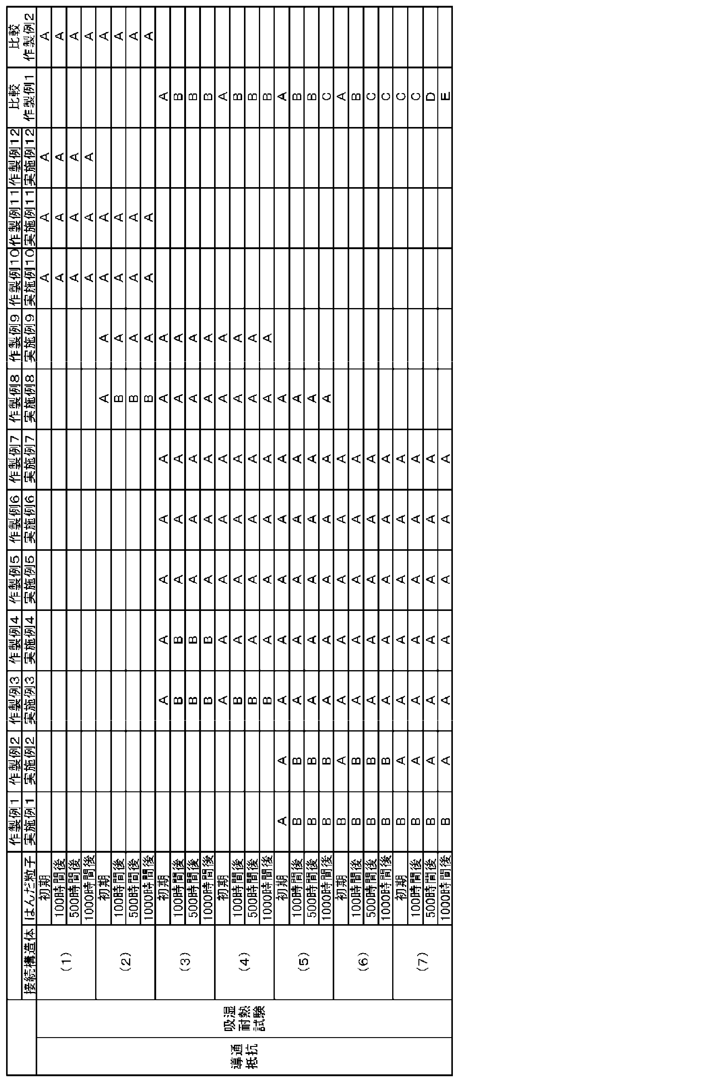
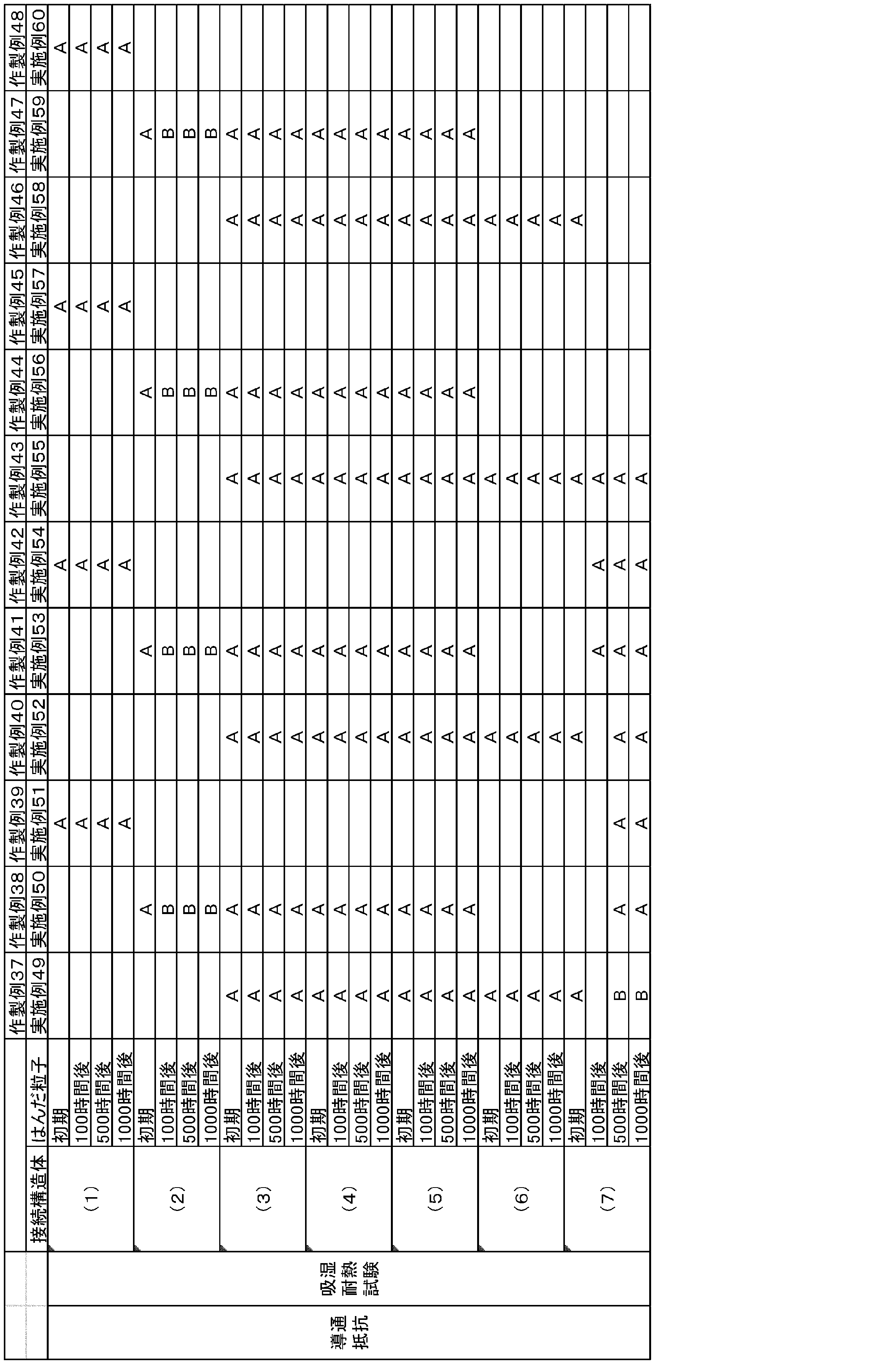
銅バンプ付きチップ(バンプ)/銅バンプ付き基板(バンプ)間の導通抵抗に関して、導通抵抗の初期値と吸湿耐熱試験(温度85℃、湿度85%の条件で100、500、1000時間放置)後の値を、20サンプルについて測定し、それらの平均値を算出した。
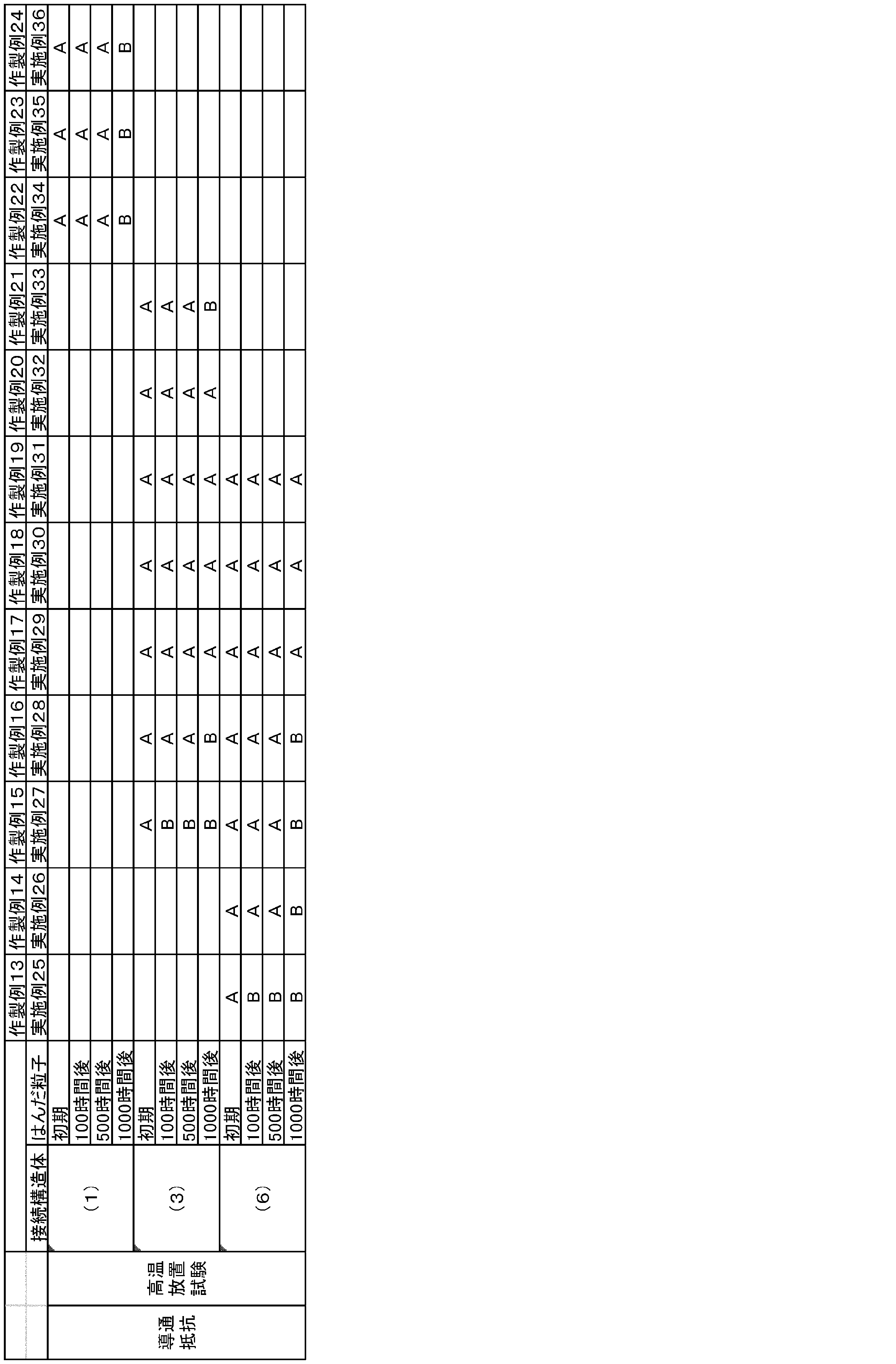
得られた平均値から下記基準に従って導通抵抗を評価した。結果を表3に示す。なお、吸湿耐熱試験1000時間後に、下記A又はBの基準を満たす場合は導通抵抗が良好といえる。
A:導通抵抗の平均値が2Ω未満
B:導通抵抗の平均値が2Ω以上5Ω未満
C:導通抵抗の平均値が5Ω以上10Ω未満
D:導通抵抗の平均値が10Ω以上20Ω未満
E:導通抵抗の平均値が20Ω以上
銅バンプ付きチップ(バンプ)/銅バンプ付き基板(バンプ)間の導通抵抗に関して、高温放置前と、高温放置試験後(温度100℃の条件で100、500、1000時間放置)のサンプルについて測定した。なお、高温放置後は、落下衝撃を加え、落下衝撃後のサンプルの導通抵抗を測定した。落下衝撃は、前記の接続構造体を、金属板にネジ止め固定し、高さ50cmから落下させた。落下後、最も衝撃の大きいチップコーナーのはんだ接合部(4箇所)において直流抵抗値を測定し、測定値が初期抵抗から5倍以上増加したときに破断が生じたとみなして、評価を行った。なお、20サンプル、4箇所で合計80箇所の測定を行った。結果を表4に示す。落下回数20回後に下記A又はBの基準を満たす場合をはんだ接続信頼性が良好であると評価した。
A:落下回数20回後において、初期抵抗から5倍以上増加したはんだ接続部が、80箇所全てにおいて認められなかった。
B:落下回数20回後において、初期抵抗から5倍以上増加したはんだ接続部が、1箇所以上5箇所以内で認められた。
C:落下回数20回後において、初期抵抗から5倍以上増加したはんだ接続部が、6箇所以上20箇所以内で認められた。
D:落下回数20回後において、初期抵抗から5倍以上増加したはんだ接続部が、21箇所以上で認められた。
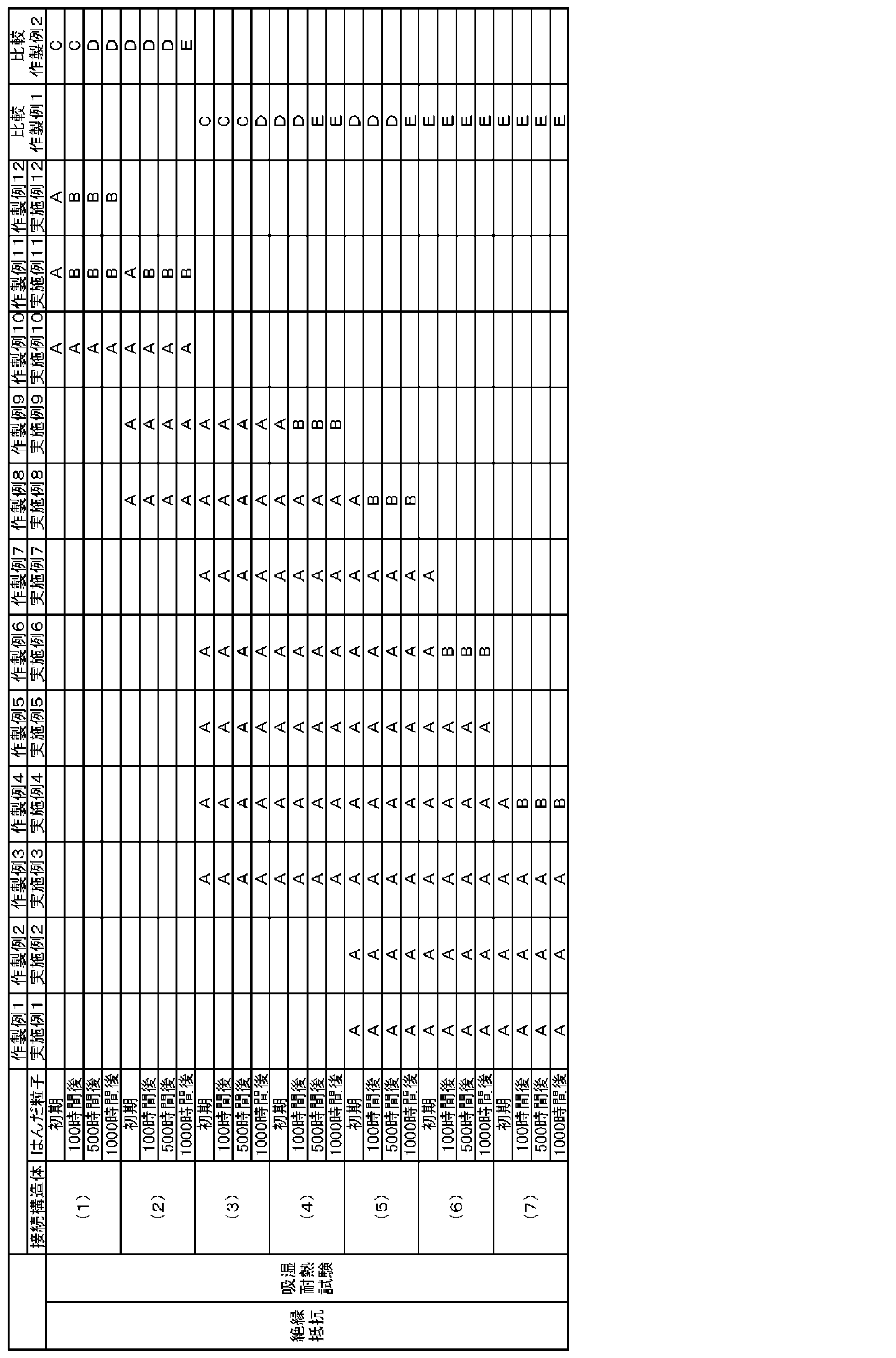
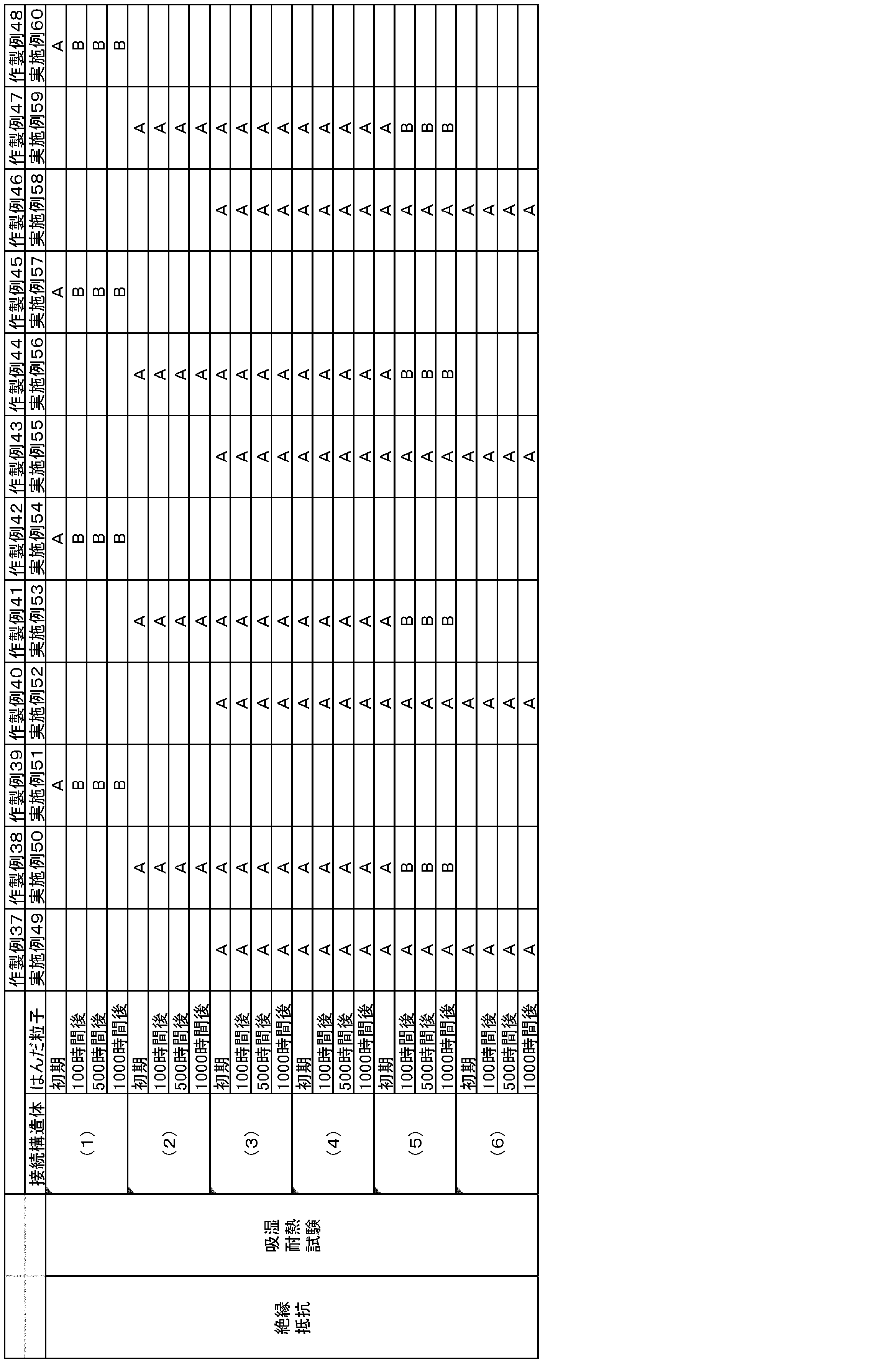
チップ電極間の絶縁抵抗に関しては、絶縁抵抗の初期値とマイグレーション試験(温度60℃、湿度90%、20V印加の条件で100、500、1000時間放置)後の値を、20サンプルについて測定し、全20サンプル中、絶縁抵抗値が109Ω以上となるサンプルの割合を算出した。得られた割合から下記基準に従って絶縁抵抗を評価した。結果を表5に示す。なお、吸湿耐熱試験1000時間後に、下記A又はBの基準を満たした場合は絶縁抵抗が良好といえる。
A:絶縁抵抗値109Ω以上の割合が100%
B:絶縁抵抗値109Ω以上の割合が90%以上100%未満
C:絶縁抵抗値109Ω以上の割合が80%以上90%未満
D:絶縁抵抗値109Ω以上の割合が50%以上80%未満
E:絶縁抵抗値109Ω以上の割合が50%未満


実施例25~36と同じ方法で作製したはんだ粒子および基体を用いたこと以外は、作製例1~12と同じ方法で異方導電性フィルム及び接続構造体の作製を行った。評価結果を表6~8に示す。


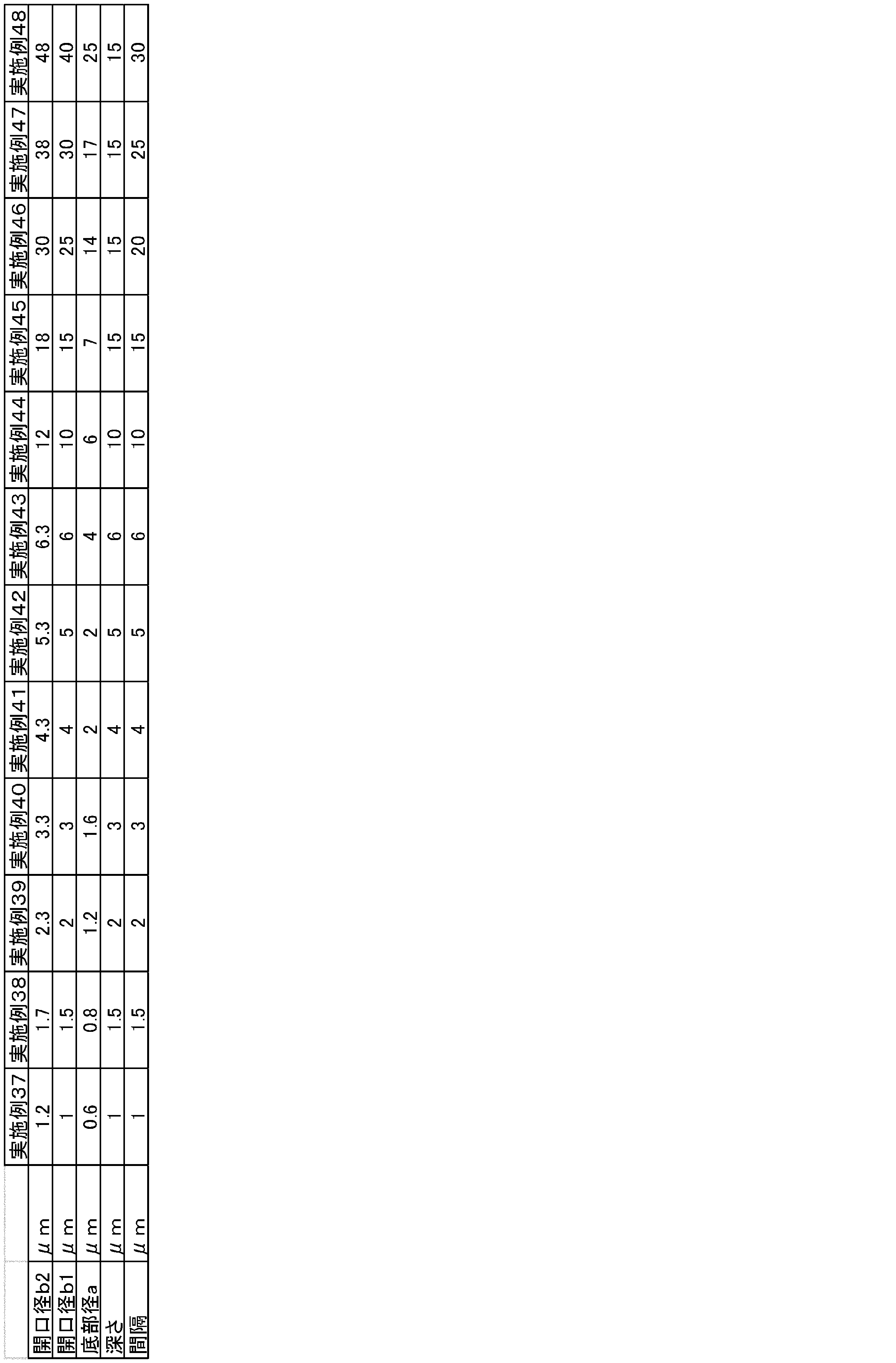
工程b1において、図8に示す断面形状(図4(b)と近似凹部形状)、すなわち底部径aが0.6μm、開口径b1が1.0μm、開口径b2が1.2μm(底部径a:1.0μmφは、開口部を上面からみると、開口径b2:1.2μmφの中央に位置する)の凹部を複数有する基体を用いたこと以外は、実施例13と同様にしてはんだ粒子を作製し、回収及び評価した。結果を表10に示す。
凹部サイズを表9に記載のとおり変更したこと以外は、実施例37と同様にしてはんだ粒子を作製し、回収及び評価した。結果を表10に示す。
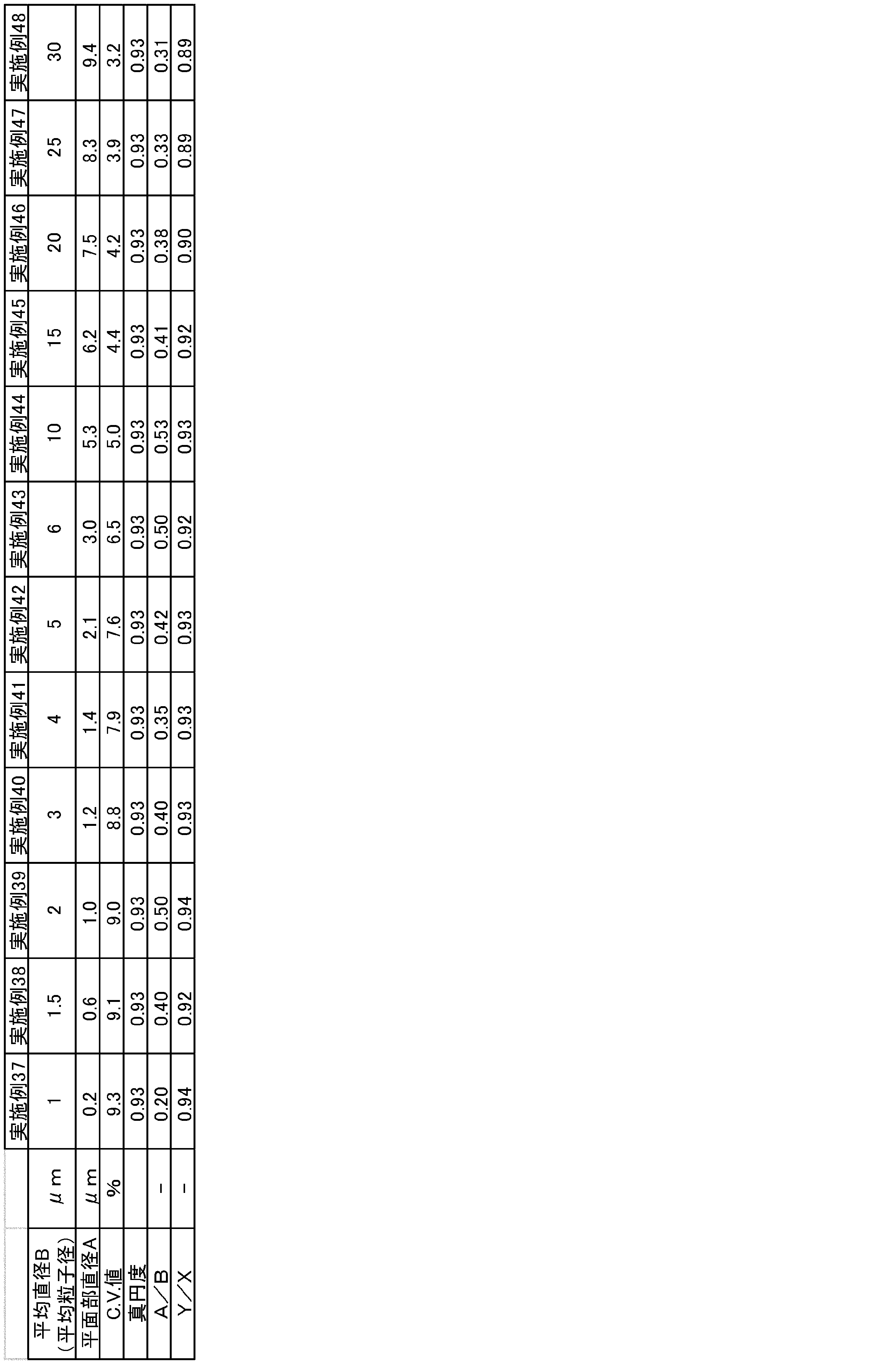
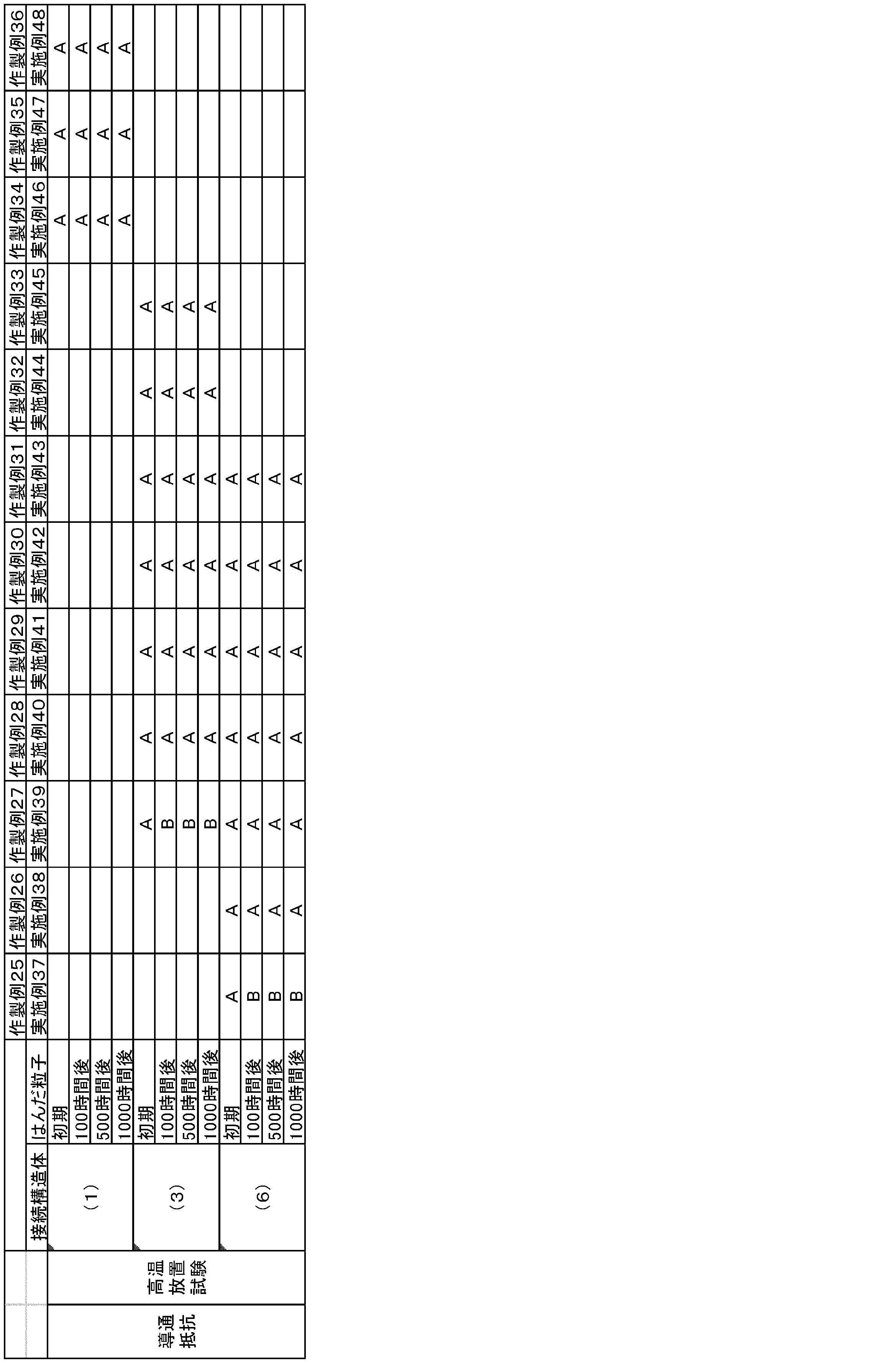
実施例37~48と同じ方法で作製したはんだ粒子および基体を用いたこと以外は、作製例1~12と同じ方法で異方導電性フィルム及び接続構造体の作製を行った。評価結果を表11~13に示す。


工程a1において、Sn-Biはんだ微粒子(5N Plus社製、融点139℃、Type9)10g、平均粒子径は3.0μm、C.V.値は32%を用いたことと、工程b1において、表14に示す凹部を用いたこと以外は、実施例13と同様にしてはんだ粒子を作製し、回収及び評価した。結果を表15に示す。
工程a1において、Sn-Biはんだ微粒子(5N Plus社製、融点139℃、Type10)10g、平均粒子径は2.8μm、C.V.値は28%を用いたことと、工程b1において、表14に示す凹部を用いたこと以外は、実施例13と同様にしてはんだ粒子を作製し、回収及び評価した。結果を表15に示す。
工程a1において、In-Snはんだ微粒子(5N Plus社製、融点120℃、Type8)100gを、蒸留水に浸漬し、超音波分散させた後、静置し、上澄みに浮遊するはんだ微粒子を回収して、平均粒子径1.0μm、C.V.値40%のはんだ微粒子を用いたことと、工程b1において、表14に示す凹部を用いたことと、工程c1に代えて、以下の工程c2を行ったこと以外は、実施例13と同様にしてはんだ粒子を作製し、回収及び評価した。結果を表15に示す。
(工程c2)はんだ粒子の形成
工程b1で凹部にはんだ微粒子が配置された基体を、水素ラジカル還元炉(新港精機株式会社製プラズマリフロー装置)に投入し、真空引き後、水素ガスを炉内に導入して、炉内を水素ガスで満たした。その後、炉内を110℃に調整し、5分間水素ラジカルを照射した。その後、真空引きにて炉内の水素ガスを除去し、160℃まで加熱した後、窒素を炉内に導入して大気圧に戻してから炉内の温度を室温まで下げることにより、はんだ粒子を形成した。
工程a1において、Sn-Ag-Cuはんだ微粒子(5N Plus社製、融点219℃、Type8)100gを、蒸留水に浸漬し、超音波分散させた後、静置し、上澄みに浮遊するはんだ微粒子を回収して、平均粒子径1.0μm、C.V.値41%のはんだ微粒子を用いたことと、工程b1において、表14に示す凹部を用いたことと、工程c1に代えて、以下の工程c2を行ったこと以外は、実施例13と同様にしてはんだ粒子を作製し、回収及び評価した。結果を表15に示す。
(工程c2)はんだ粒子の形成
工程b1で凹部にはんだ微粒子が配置された基体を、水素ラジカル還元炉(新港精機株式会社製プラズマリフロー装置)に投入し、真空引き後、水素ガスを炉内に導入して、炉内を水素ガスで満たした。その後、炉内を150℃に調整し、3分間水素ラジカルを照射した。その後、真空引きにて炉内の水素ガスを除去し、240℃まで加熱した後、窒素を炉内に導入して大気圧に戻してから炉内の温度を室温まで下げることにより、はんだ粒子を形成した。
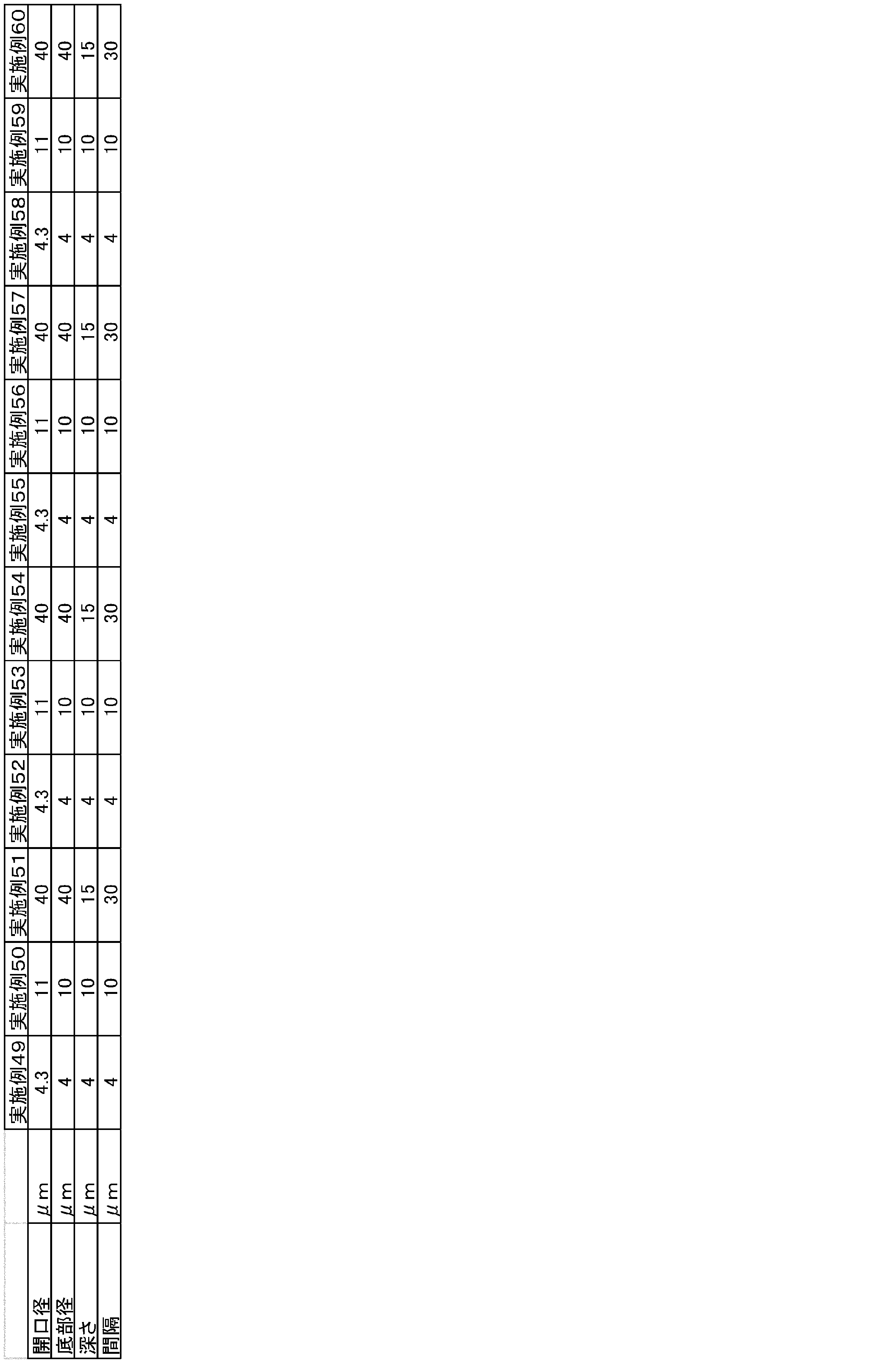

実施例49~51と同じ方法で作製したはんだ粒子を用いたこと以外は、試作例1と同じ方法で異方導電性フィルム及び接続構造体の作製を行った。結果を表16~18に示す。
実施例52~54と同じ方法で作製したはんだ粒子を用いたこと以外は、試作例1と同じ方法で異方導電性フィルム及び接続構造体の作製を行った。結果を表16~18に示す。
実施例55~57と同じ方法で作製したはんだ粒子を用いたこと以外は、試作例1と同じ方法で異方導電性フィルム及び接続構造体の作製を行った。結果を表16~18に示す。
実施例58~60と同じ方法で作製したはんだ粒子を用いたこと、及び、工程l1において、本圧着温度を230℃にしたこと以外は、実施例1と同じ方法で異方導電性フィルム及び接続構造体の作製を行った。結果を表16~18に示す。

本願の方法であれば、はんだ微粒子の組成を変更するだけで、粒子径がそろった融点の異なるはんだ粒子を容易に得られる。また、凹部の断面形状は各種用いることが出来る。すなわち、はんだ粒子の最終利用方法や形態に合わせて凹部の断面形状は適宜選択出来る。例えば、樹脂中にはんだ粒子を分散し、インクのように流動性を確保する場合は、はんだ粒子の表面は連続曲面を有している方が好ましいと考えられる。一方、フィルム中にはんだ粒子を分散し、圧着工程により電極にはんだ粒子を接触させる場合、電極の形状や材質によって、はんだ粒子に平面部があると、接触時の電極への衝撃を緩和し、電極の破損を防ぐことが出来る。また、圧着工程で加熱により粘度が低下した樹脂が流動し、電極上から動いてしまうことがあるが、平面部を有する場合、電極との接触面積が高くなりやすく、フラックスによる酸化被膜除去時に素早く電極への濡れが広がるため、樹脂流動による移動が抑制出来る利点もある。樹脂ペーストにおいても同様の現象がみられる。さらに、本願作製例で得られる、一部に平坦部を有するはんだ粒子を、接着樹脂フィルムに転写もしくは、基体に接着樹脂を流し込んでフィルム化したのち、基体を除去すると、フィルム内において、はんだ粒子の平坦部の向きが略同一方向にそろえることが出来る。このようなはんだ粒子入り接着樹脂フィルムを用いて、電極同士を圧着実装した場合、非常に薄く、または弱い材質で出来た電極に対して、平坦部の面により接触するため、電極破損を抑制することが出来る。また、濡れ広がりが難しい電極に対しても、圧着時に平坦部が面で接触することで、球面の点接触よりもはんだ粒子の酸化被膜の除去による濡れ広がりが起こりやすい利点がある。実利用上、接続したい電極同士は、その構成も材質も異なる場合が一般的で、本願のように、はんだ粒子の平坦部などの向きを概ねそろえられる特徴は、電極材質に合わせて、接着樹脂フィルムの配置位置を選択してより確実な接続を実現できる特徴がある。
実施例46、47、48で得たはんだ粒子を、開口部がそれぞれ6μm、14μm、40μmのマスクを介して、スパッタによって形成された縦横10μm、20μm、50μmのAu電極上に配置した。このAu電極が形成された基板を15度、20度、30度、45度に傾け、金属へらでたたいて振動を加えた。振動を加えたのち、電極上を観察したところ、電極上に残っていたはんだ粒子は、平坦部がAu電極面と接していた粒子であった。
Claims (6)
- 表面の一部に平面部を有する、はんだ粒子。
- 平均粒子径が1~30μmであり、かつC.V.値が20%以下である、請求項1に記載のはんだ粒子。
- 前記はんだ粒子の直径Bに対する前記平面部の直径Aの比(A/B)が下記式を満たす、請求項1又は2に記載のはんだ粒子。
0.01<A/B<1.0 - はんだ粒子の投影像に外接する四角形を二対の平行線により作成した場合において、対向する辺間の距離をX及びY(但しY<X)としたときに、X及びYが下記式を満たす、請求項1~3のいずれか一項に記載のはんだ粒子。
0.8<Y/X<1.0 - スズ、スズ合金、インジウム及びインジウム合金からなる群より選択される少なくとも一種を含む、請求項1~4のいずれか一項に記載のはんだ粒子。
- In-Sn合金、In-Sn-Ag合金、In-Bi合金、Sn-Au合金、Sn-Bi合金、Sn-Bi-Ag合金、Sn-Ag-Cu合金及びSn-Cu合金からなる群より選択される少なくとも一種を含む、請求項5に記載のはんだ粒子。
Priority Applications (6)
| Application Number | Priority Date | Filing Date | Title |
|---|---|---|---|
| KR1020217001585A KR102856173B1 (ko) | 2018-06-26 | 2019-06-26 | 땜납 입자 |
| JP2020527609A JPWO2020004513A1 (ja) | 2018-06-26 | 2019-06-26 | はんだ粒子 |
| US17/255,982 US12172240B2 (en) | 2018-06-26 | 2019-06-26 | Solder particles |
| CN201980041928.5A CN112543693A (zh) | 2018-06-26 | 2019-06-26 | 焊料粒子 |
| JP2023126432A JP2023153934A (ja) | 2018-06-26 | 2023-08-02 | はんだ粒子 |
| JP2025021206A JP2025069455A (ja) | 2018-06-26 | 2025-02-13 | はんだ粒子 |
Applications Claiming Priority (4)
| Application Number | Priority Date | Filing Date | Title |
|---|---|---|---|
| JP2018-121088 | 2018-06-26 | ||
| JP2018121088 | 2018-06-26 | ||
| JP2019-014853 | 2019-01-30 | ||
| JP2019014853 | 2019-01-30 |
Publications (1)
| Publication Number | Publication Date |
|---|---|
| WO2020004513A1 true WO2020004513A1 (ja) | 2020-01-02 |
Family
ID=68984541
Family Applications (1)
| Application Number | Title | Priority Date | Filing Date |
|---|---|---|---|
| PCT/JP2019/025499 Ceased WO2020004513A1 (ja) | 2018-06-26 | 2019-06-26 | はんだ粒子 |
Country Status (6)
| Country | Link |
|---|---|
| US (1) | US12172240B2 (ja) |
| JP (3) | JPWO2020004513A1 (ja) |
| KR (1) | KR102856173B1 (ja) |
| CN (1) | CN112543693A (ja) |
| TW (2) | TWI835813B (ja) |
| WO (1) | WO2020004513A1 (ja) |
Cited By (4)
| Publication number | Priority date | Publication date | Assignee | Title |
|---|---|---|---|---|
| WO2022107800A1 (ja) * | 2020-11-20 | 2022-05-27 | 昭和電工マテリアルズ株式会社 | 回路接続用接着剤フィルム、並びに、接続構造体及びその製造方法 |
| US20230042727A1 (en) * | 2019-12-27 | 2023-02-09 | Showa Denko Materials Co., Ltd. | Solder bump forming member, method for manufacturing solder bump forming member, and method for manufacturing electrode substrate provided with solder bump |
| WO2023026754A1 (ja) * | 2021-08-27 | 2023-03-02 | デクセリアルズ株式会社 | はんだ粒子、はんだ粒子の製造方法、及び導電性組成物 |
| TWI917477B (zh) | 2020-11-20 | 2026-03-11 | 日商力森諾科股份有限公司 | 電路連接用接著劑薄膜、以及連接結構體及其製造方法 |
Families Citing this family (1)
| Publication number | Priority date | Publication date | Assignee | Title |
|---|---|---|---|---|
| JP7080939B2 (ja) * | 2020-09-04 | 2022-06-06 | 株式会社新菱 | 低融点接合部材およびその製造方法ならびに半導体電子回路およびその実装方法 |
Citations (3)
| Publication number | Priority date | Publication date | Assignee | Title |
|---|---|---|---|---|
| JPH01184201A (ja) * | 1988-01-14 | 1989-07-21 | Electroplating Eng Of Japan Co | 金属パウダー及びそのペースト |
| JPH0523887A (ja) * | 1991-07-19 | 1993-02-02 | Matsushita Electric Ind Co Ltd | 金属ボールの形成方法 |
| JP2010036234A (ja) * | 2008-08-07 | 2010-02-18 | Mitsui Mining & Smelting Co Ltd | はんだ粉及びはんだペースト |
Family Cites Families (70)
| Publication number | Priority date | Publication date | Assignee | Title |
|---|---|---|---|---|
| JPH0221177Y2 (ja) | 1984-11-10 | 1990-06-07 | ||
| JP2740699B2 (ja) * | 1991-07-08 | 1998-04-15 | アルプス電気株式会社 | 端子接続構造、端子接続方法および導電性粒子製造方法 |
| US5527628A (en) | 1993-07-20 | 1996-06-18 | Iowa State University Research Foudation, Inc. | Pb-free Sn-Ag-Cu ternary eutectic solder |
| US6025258A (en) | 1994-01-20 | 2000-02-15 | Fujitsu Limited | Method for fabricating solder bumps by forming solder balls with a solder ball forming member |
| US5542174A (en) | 1994-09-15 | 1996-08-06 | Intel Corporation | Method and apparatus for forming solder balls and solder columns |
| US5736074A (en) | 1995-06-30 | 1998-04-07 | Micro Fab Technologies, Inc. | Manufacture of coated spheres |
| JP2798011B2 (ja) | 1995-07-10 | 1998-09-17 | 日本電気株式会社 | 半田ボール |
| JP2973889B2 (ja) * | 1995-09-13 | 1999-11-08 | 松下電器産業株式会社 | 導電性ボールの搭載装置および搭載方法 |
| JPH09150296A (ja) | 1995-11-27 | 1997-06-10 | Nec Corp | 金属ボールの形成方法 |
| JPH1013007A (ja) * | 1996-03-29 | 1998-01-16 | Ngk Spark Plug Co Ltd | 半田バンプを有する配線基板及びその製造方法及び平坦化治具 |
| US6293456B1 (en) | 1997-05-27 | 2001-09-25 | Spheretek, Llc | Methods for forming solder balls on substrates |
| US7007833B2 (en) | 1997-05-27 | 2006-03-07 | Mackay John | Forming solder balls on substrates |
| JP3420917B2 (ja) | 1997-09-08 | 2003-06-30 | 富士通株式会社 | 半導体装置 |
| US6189772B1 (en) | 1998-08-31 | 2001-02-20 | Micron Technology, Inc. | Method of forming a solder ball |
| CN1069757C (zh) | 1998-11-06 | 2001-08-15 | 杨洋鑫 | 一种安全鞭炮 |
| US6523736B1 (en) | 1998-12-11 | 2003-02-25 | Micron Technology, Inc. | Methods and apparatus for forming solder balls |
| TW557237B (en) | 2001-09-14 | 2003-10-11 | Sekisui Chemical Co Ltd | Coated conductive particle, coated conductive particle manufacturing method, anisotropic conductive material, and conductive connection structure |
| CN1253279C (zh) | 2001-10-26 | 2006-04-26 | 宫崎县 | 单分散球形金属粒子及其生产方法 |
| US6802446B2 (en) | 2002-02-01 | 2004-10-12 | Delphi Technologies, Inc. | Conductive adhesive material with metallurgically-bonded conductive particles |
| US20040016456A1 (en) | 2002-07-25 | 2004-01-29 | Clean Venture 21 Corporation | Photovoltaic device and method for producing the same |
| JP3869785B2 (ja) | 2002-10-25 | 2007-01-17 | 積水化学工業株式会社 | 絶縁被覆導電性微粒子及び導電接続構造体 |
| JP2005019393A (ja) | 2003-06-05 | 2005-01-20 | Sharp Corp | 異方性導電物、表示装置、表示装置の製造方法および導電部材 |
| CN100454529C (zh) * | 2003-10-24 | 2009-01-21 | 国际整流器公司 | 用于形成互连结构的焊膏以及由焊膏形成的互连结构 |
| JP2005183904A (ja) | 2003-12-22 | 2005-07-07 | Rohm & Haas Electronic Materials Llc | 電子部品にはんだ領域を形成する方法及びはんだ領域を有する電子部品 |
| WO2006043377A1 (ja) * | 2004-10-19 | 2006-04-27 | Senju Metal Industry Co., Ltd. | はんだバンプ形成用シートとその製造方法 |
| WO2006085481A1 (ja) | 2005-02-09 | 2006-08-17 | Sekisui Chemical Co., Ltd. | 導電性微粒子、異方性導電材料、及び導電接続方法 |
| JP4084834B2 (ja) | 2005-03-29 | 2008-04-30 | 松下電器産業株式会社 | フリップチップ実装方法およびバンプ形成方法 |
| JP4872663B2 (ja) | 2006-12-28 | 2012-02-08 | 株式会社日立製作所 | 接合用材料及び接合方法 |
| WO2008111615A1 (ja) | 2007-03-12 | 2008-09-18 | Senju Metal Industry Co., Ltd. | 異方性導電材料 |
| JP2009167436A (ja) | 2008-01-10 | 2009-07-30 | Hitachi Ltd | 接合用材料および接合形成方法 |
| JP5456545B2 (ja) | 2009-04-28 | 2014-04-02 | 昭和電工株式会社 | 回路基板の製造方法 |
| KR101162890B1 (ko) | 2010-03-17 | 2012-07-05 | 세키스이가가쿠 고교가부시키가이샤 | 도전성 입자, 도전성 입자의 제조 방법, 이방성 도전 재료 및 접속 구조체 |
| JP5690554B2 (ja) | 2010-10-27 | 2015-03-25 | 昭和電工株式会社 | はんだボールの製造方法 |
| JP5320523B1 (ja) | 2012-02-21 | 2013-10-23 | 積水化学工業株式会社 | 導電性粒子、導電性粒子の製造方法、導電材料及び接続構造体 |
| KR101380454B1 (ko) | 2012-03-26 | 2014-04-01 | 세키스이가가쿠 고교가부시키가이샤 | 도전 재료 및 접속 구조체 |
| JP5939063B2 (ja) | 2012-07-11 | 2016-06-22 | 日立化成株式会社 | 絶縁被覆導電粒子及びそれを用いた異方導電性接着剤 |
| JP6024621B2 (ja) | 2012-08-24 | 2016-11-16 | デクセリアルズ株式会社 | 異方性導電フィルムの製造方法及び異方性導電フィルム |
| KR102056086B1 (ko) | 2012-08-24 | 2019-12-16 | 데쿠세리아루즈 가부시키가이샤 | 이방성 도전 필름 및 그의 제조 방법 |
| JP2014058147A (ja) * | 2012-09-19 | 2014-04-03 | Tokyo Ohka Kogyo Co Ltd | はんだ球製造用のモールドの製造方法、及びはんだ球の製造方法 |
| JP2014060368A (ja) | 2012-09-19 | 2014-04-03 | Tokyo Ohka Kogyo Co Ltd | はんだ球製造用のモールドの製造方法、及びはんだ球の製造方法 |
| JP6007796B2 (ja) | 2013-01-09 | 2016-10-12 | ソニー株式会社 | 回路基板の製造方法 |
| US20160155717A1 (en) | 2013-07-31 | 2016-06-02 | Dexerials Corporation | Anisotropic conductive film and manufacturing method therefor |
| JP2015131340A (ja) * | 2013-12-10 | 2015-07-23 | 住友金属鉱山株式会社 | Au−Sn−Ag系はんだ合金並びにこのAu−Sn−Ag系はんだ合金を用いて封止された電子部品及び電子部品搭載装置 |
| JP2015136735A (ja) * | 2014-01-24 | 2015-07-30 | 住友金属鉱山株式会社 | ボール状Au−Sn−Ag系はんだ合金並びにこのボール状Au−Sn−Ag系はんだ合金を用いて封止された電子部品及び電子部品搭載装置 |
| JP5585751B1 (ja) | 2014-02-04 | 2014-09-10 | 千住金属工業株式会社 | Cuボール、Cu核ボール、はんだ継手、はんだペースト、およびフォームはんだ |
| JP5830196B1 (ja) | 2014-02-24 | 2015-12-09 | 積水化学工業株式会社 | 導電ペースト、接続構造体及び接続構造体の製造方法 |
| JP2015220396A (ja) | 2014-05-20 | 2015-12-07 | 三菱マテリアル株式会社 | はんだバンプの形成方法及びはんだボール固定用はんだペースト |
| JP7052254B2 (ja) | 2016-11-04 | 2022-04-12 | デクセリアルズ株式会社 | フィラー含有フィルム |
| JP6661969B2 (ja) | 2014-10-28 | 2020-03-11 | デクセリアルズ株式会社 | 異方性導電フィルム及び接続構造体 |
| KR20170090353A (ko) | 2014-11-20 | 2017-08-07 | 세키스이가가쿠 고교가부시키가이샤 | 도전성 입자, 도전성 입자의 제조 방법, 도전 재료 및 접속 구조체 |
| JP2016126878A (ja) * | 2014-12-26 | 2016-07-11 | 積水化学工業株式会社 | 導電ペースト、接続構造体及び接続構造体の製造方法 |
| KR102398451B1 (ko) | 2015-01-13 | 2022-05-16 | 데쿠세리아루즈 가부시키가이샤 | 범프 형성용 필름, 반도체 장치 및 그의 제조 방법 및 접속 구조체 |
| TWI709221B (zh) | 2015-01-13 | 2020-11-01 | 日商迪睿合股份有限公司 | 多層基板及其製造方法、及各向異性導電膜 |
| JP6458503B2 (ja) | 2015-01-13 | 2019-01-30 | デクセリアルズ株式会社 | 異方性導電フィルム、その製造方法及び接続構造体 |
| WO2016133113A1 (ja) | 2015-02-19 | 2016-08-25 | 積水化学工業株式会社 | 導電ペースト及び接続構造体 |
| JPWO2017033933A1 (ja) | 2015-08-24 | 2018-06-07 | 積水化学工業株式会社 | 導電材料及び接続構造体 |
| JP6581434B2 (ja) * | 2015-08-24 | 2019-09-25 | 積水化学工業株式会社 | 導電材料及び接続構造体 |
| KR102429873B1 (ko) | 2015-08-31 | 2022-08-05 | 삼성전자주식회사 | 이방성 도전 재료와 이방성 도전 재료를 포함하는 전자소자 및 그 제조방법 |
| JP2017195180A (ja) | 2016-04-19 | 2017-10-26 | 積水化学工業株式会社 | 導電材料及び接続構造体 |
| JP7284555B2 (ja) | 2016-09-09 | 2023-05-31 | 積水化学工業株式会社 | 導電材料、接続構造体及び接続構造体の製造方法 |
| JP6187665B1 (ja) | 2016-10-18 | 2017-08-30 | デクセリアルズ株式会社 | 異方性導電フィルム |
| US20200299474A1 (en) | 2016-10-18 | 2020-09-24 | Dexerials Corporation | Filler-containing film |
| CN114221146B (zh) | 2016-11-30 | 2024-11-22 | 迪睿合株式会社 | 导电粒子配置膜、其制造方法、检查探头单元、导通检查方法 |
| KR101877931B1 (ko) * | 2016-12-06 | 2018-07-12 | 주식회사 테토스 | 솔더 입자의 제조 방법 |
| JP2019029135A (ja) * | 2017-07-27 | 2019-02-21 | 日立化成株式会社 | 異方性導電フィルム及びその製造方法、並びに接続構造体及びその製造方法 |
| JP7046351B2 (ja) | 2018-01-31 | 2022-04-04 | 三国電子有限会社 | 接続構造体の作製方法 |
| CN112292430A (zh) | 2018-06-06 | 2021-01-29 | 迪睿合株式会社 | 含有填料的膜 |
| TWI886097B (zh) * | 2018-06-26 | 2025-06-11 | 日商力森諾科股份有限公司 | 焊料粒及焊料粒的製造方法 |
| WO2020004510A1 (ja) | 2018-06-26 | 2020-01-02 | 日立化成株式会社 | 異方性導電フィルム及びその製造方法並びに接続構造体の製造方法 |
| US11916003B2 (en) | 2019-09-18 | 2024-02-27 | Intel Corporation | Varied ball ball-grid-array (BGA) packages |
-
2019
- 2019-06-26 CN CN201980041928.5A patent/CN112543693A/zh active Pending
- 2019-06-26 JP JP2020527609A patent/JPWO2020004513A1/ja active Pending
- 2019-06-26 TW TW108122479A patent/TWI835813B/zh active
- 2019-06-26 WO PCT/JP2019/025499 patent/WO2020004513A1/ja not_active Ceased
- 2019-06-26 KR KR1020217001585A patent/KR102856173B1/ko active Active
- 2019-06-26 TW TW113106460A patent/TWI904579B/zh active
- 2019-06-26 US US17/255,982 patent/US12172240B2/en active Active
-
2023
- 2023-08-02 JP JP2023126432A patent/JP2023153934A/ja not_active Withdrawn
-
2025
- 2025-02-13 JP JP2025021206A patent/JP2025069455A/ja active Pending
Patent Citations (3)
| Publication number | Priority date | Publication date | Assignee | Title |
|---|---|---|---|---|
| JPH01184201A (ja) * | 1988-01-14 | 1989-07-21 | Electroplating Eng Of Japan Co | 金属パウダー及びそのペースト |
| JPH0523887A (ja) * | 1991-07-19 | 1993-02-02 | Matsushita Electric Ind Co Ltd | 金属ボールの形成方法 |
| JP2010036234A (ja) * | 2008-08-07 | 2010-02-18 | Mitsui Mining & Smelting Co Ltd | はんだ粉及びはんだペースト |
Cited By (9)
| Publication number | Priority date | Publication date | Assignee | Title |
|---|---|---|---|---|
| US20230042727A1 (en) * | 2019-12-27 | 2023-02-09 | Showa Denko Materials Co., Ltd. | Solder bump forming member, method for manufacturing solder bump forming member, and method for manufacturing electrode substrate provided with solder bump |
| US12246398B2 (en) * | 2019-12-27 | 2025-03-11 | Resonac Corporation | Solder bump forming member, method for manufacturing solder bump forming member, and method for manufacturing electrode substrate provided with solder bump |
| WO2022107800A1 (ja) * | 2020-11-20 | 2022-05-27 | 昭和電工マテリアルズ株式会社 | 回路接続用接着剤フィルム、並びに、接続構造体及びその製造方法 |
| JPWO2022107800A1 (ja) * | 2020-11-20 | 2022-05-27 | ||
| JP7798036B2 (ja) | 2020-11-20 | 2026-01-14 | 株式会社レゾナック | 回路接続用接着剤フィルム、並びに、接続構造体及びその製造方法 |
| TWI917477B (zh) | 2020-11-20 | 2026-03-11 | 日商力森諾科股份有限公司 | 電路連接用接著劑薄膜、以及連接結構體及其製造方法 |
| WO2023026754A1 (ja) * | 2021-08-27 | 2023-03-02 | デクセリアルズ株式会社 | はんだ粒子、はんだ粒子の製造方法、及び導電性組成物 |
| JP2023032620A (ja) * | 2021-08-27 | 2023-03-09 | デクセリアルズ株式会社 | はんだ粒子、はんだ粒子の製造方法、及び導電性組成物 |
| JP7775559B2 (ja) | 2021-08-27 | 2025-11-26 | デクセリアルズ株式会社 | はんだ粒子、はんだ粒子の製造方法、及び導電性組成物 |
Also Published As
| Publication number | Publication date |
|---|---|
| TW202000939A (zh) | 2020-01-01 |
| CN112543693A (zh) | 2021-03-23 |
| TW202428901A (zh) | 2024-07-16 |
| US20210114145A1 (en) | 2021-04-22 |
| TWI835813B (zh) | 2024-03-21 |
| TWI904579B (zh) | 2025-11-11 |
| KR102856173B1 (ko) | 2025-09-04 |
| KR20210024024A (ko) | 2021-03-04 |
| JP2025069455A (ja) | 2025-04-30 |
| JP2023153934A (ja) | 2023-10-18 |
| US12172240B2 (en) | 2024-12-24 |
| JPWO2020004513A1 (ja) | 2021-08-02 |
Similar Documents
| Publication | Publication Date | Title |
|---|---|---|
| JP7452419B2 (ja) | はんだ粒子及びはんだ粒子の製造方法 | |
| JP7452418B2 (ja) | 異方性導電フィルム及びその製造方法並びに接続構造体の製造方法 | |
| JP2023153934A (ja) | はんだ粒子 | |
| JP2025069454A (ja) | はんだペースト | |
| US20250083262A1 (en) | Solder particles and method for producing solder particles | |
| JP7480789B2 (ja) | 接続構造体及び接続構造体の製造方法 | |
| JP7400465B2 (ja) | コアシェル型はんだ粒子、コアシェル型はんだ粒子の製造方法、異方性導電フィルム、及び異方性導電フィルムの製造方法 | |
| JP7768127B2 (ja) | はんだ粒子、はんだ粒子の製造方法及びはんだ粒子付き基体 | |
| JP2021108347A (ja) | 接続構造体の製造方法 |
Legal Events
| Date | Code | Title | Description |
|---|---|---|---|
| 121 | Ep: the epo has been informed by wipo that ep was designated in this application |
Ref document number: 19825985 Country of ref document: EP Kind code of ref document: A1 |
|
| ENP | Entry into the national phase |
Ref document number: 2020527609 Country of ref document: JP Kind code of ref document: A |
|
| NENP | Non-entry into the national phase |
Ref country code: DE |
|
| ENP | Entry into the national phase |
Ref document number: 20217001585 Country of ref document: KR Kind code of ref document: A |
|
| 122 | Ep: pct application non-entry in european phase |
Ref document number: 19825985 Country of ref document: EP Kind code of ref document: A1 |