WO2019229802A1 - 半導体装置の製造方法 - Google Patents
半導体装置の製造方法 Download PDFInfo
- Publication number
- WO2019229802A1 WO2019229802A1 PCT/JP2018/020353 JP2018020353W WO2019229802A1 WO 2019229802 A1 WO2019229802 A1 WO 2019229802A1 JP 2018020353 W JP2018020353 W JP 2018020353W WO 2019229802 A1 WO2019229802 A1 WO 2019229802A1
- Authority
- WO
- WIPO (PCT)
- Prior art keywords
- resin film
- semiconductor device
- photosensitive resin
- manufacturing
- dicing line
- Prior art date
- Legal status (The legal status is an assumption and is not a legal conclusion. Google has not performed a legal analysis and makes no representation as to the accuracy of the status listed.)
- Ceased
Links
Images







Classifications
-
- H—ELECTRICITY
- H10—SEMICONDUCTOR DEVICES; ELECTRIC SOLID-STATE DEVICES NOT OTHERWISE PROVIDED FOR
- H10W—GENERIC PACKAGES, INTERCONNECTIONS, CONNECTORS OR OTHER CONSTRUCTIONAL DETAILS OF DEVICES COVERED BY CLASS H10
- H10W74/00—Encapsulations, e.g. protective coatings
- H10W74/01—Manufacture or treatment
- H10W74/019—Manufacture or treatment using temporary auxiliary substrates
-
- H—ELECTRICITY
- H10—SEMICONDUCTOR DEVICES; ELECTRIC SOLID-STATE DEVICES NOT OTHERWISE PROVIDED FOR
- H10P—GENERIC PROCESSES OR APPARATUS FOR THE MANUFACTURE OR TREATMENT OF DEVICES COVERED BY CLASS H10
- H10P54/00—Cutting or separating of wafers, substrates or parts of devices
-
- H—ELECTRICITY
- H10—SEMICONDUCTOR DEVICES; ELECTRIC SOLID-STATE DEVICES NOT OTHERWISE PROVIDED FOR
- H10D—INORGANIC ELECTRIC SEMICONDUCTOR DEVICES
- H10D64/00—Electrodes of devices having potential barriers
- H10D64/01—Manufacture or treatment
- H10D64/013—Manufacture or treatment of electrodes having a conductor capacitively coupled to a semiconductor by an insulator
- H10D64/01302—Manufacture or treatment of electrodes having a conductor capacitively coupled to a semiconductor by an insulator the insulator being formed after the semiconductor body, the semiconductor being silicon
- H10D64/01304—Manufacture or treatment of electrodes having a conductor capacitively coupled to a semiconductor by an insulator the insulator being formed after the semiconductor body, the semiconductor being silicon characterised by the conductor
- H10D64/01324—Manufacture or treatment of electrodes having a conductor capacitively coupled to a semiconductor by an insulator the insulator being formed after the semiconductor body, the semiconductor being silicon characterised by the conductor characterised by the sectional shape, e.g. T or inverted-T
-
- H—ELECTRICITY
- H10—SEMICONDUCTOR DEVICES; ELECTRIC SOLID-STATE DEVICES NOT OTHERWISE PROVIDED FOR
- H10W—GENERIC PACKAGES, INTERCONNECTIONS, CONNECTORS OR OTHER CONSTRUCTIONAL DETAILS OF DEVICES COVERED BY CLASS H10
- H10W20/00—Interconnections in chips, wafers or substrates
- H10W20/01—Manufacture or treatment
- H10W20/031—Manufacture or treatment of conductive parts of the interconnections
- H10W20/0698—Local interconnections
-
- H—ELECTRICITY
- H10—SEMICONDUCTOR DEVICES; ELECTRIC SOLID-STATE DEVICES NOT OTHERWISE PROVIDED FOR
- H10W—GENERIC PACKAGES, INTERCONNECTIONS, CONNECTORS OR OTHER CONSTRUCTIONAL DETAILS OF DEVICES COVERED BY CLASS H10
- H10W20/00—Interconnections in chips, wafers or substrates
- H10W20/01—Manufacture or treatment
- H10W20/071—Manufacture or treatment of dielectric parts thereof
-
- H—ELECTRICITY
- H10—SEMICONDUCTOR DEVICES; ELECTRIC SOLID-STATE DEVICES NOT OTHERWISE PROVIDED FOR
- H10W—GENERIC PACKAGES, INTERCONNECTIONS, CONNECTORS OR OTHER CONSTRUCTIONAL DETAILS OF DEVICES COVERED BY CLASS H10
- H10W20/00—Interconnections in chips, wafers or substrates
- H10W20/01—Manufacture or treatment
- H10W20/071—Manufacture or treatment of dielectric parts thereof
- H10W20/072—Manufacture or treatment of dielectric parts thereof of dielectric parts comprising air gaps
-
- H—ELECTRICITY
- H10—SEMICONDUCTOR DEVICES; ELECTRIC SOLID-STATE DEVICES NOT OTHERWISE PROVIDED FOR
- H10W—GENERIC PACKAGES, INTERCONNECTIONS, CONNECTORS OR OTHER CONSTRUCTIONAL DETAILS OF DEVICES COVERED BY CLASS H10
- H10W20/00—Interconnections in chips, wafers or substrates
- H10W20/01—Manufacture or treatment
- H10W20/071—Manufacture or treatment of dielectric parts thereof
- H10W20/081—Manufacture or treatment of dielectric parts thereof by forming openings in the dielectric parts
- H10W20/083—Manufacture or treatment of dielectric parts thereof by forming openings in the dielectric parts the openings being via holes penetrating underlying conductors
-
- H—ELECTRICITY
- H10—SEMICONDUCTOR DEVICES; ELECTRIC SOLID-STATE DEVICES NOT OTHERWISE PROVIDED FOR
- H10W—GENERIC PACKAGES, INTERCONNECTIONS, CONNECTORS OR OTHER CONSTRUCTIONAL DETAILS OF DEVICES COVERED BY CLASS H10
- H10W20/00—Interconnections in chips, wafers or substrates
- H10W20/01—Manufacture or treatment
- H10W20/071—Manufacture or treatment of dielectric parts thereof
- H10W20/081—Manufacture or treatment of dielectric parts thereof by forming openings in the dielectric parts
- H10W20/084—Manufacture or treatment of dielectric parts thereof by forming openings in the dielectric parts for dual-damascene structures
-
- H—ELECTRICITY
- H10—SEMICONDUCTOR DEVICES; ELECTRIC SOLID-STATE DEVICES NOT OTHERWISE PROVIDED FOR
- H10W—GENERIC PACKAGES, INTERCONNECTIONS, CONNECTORS OR OTHER CONSTRUCTIONAL DETAILS OF DEVICES COVERED BY CLASS H10
- H10W20/00—Interconnections in chips, wafers or substrates
- H10W20/40—Interconnections external to wafers or substrates, e.g. back-end-of-line [BEOL] metallisations or vias connecting to gate electrodes
- H10W20/45—Interconnections external to wafers or substrates, e.g. back-end-of-line [BEOL] metallisations or vias connecting to gate electrodes characterised by their insulating parts
- H10W20/46—Interconnections external to wafers or substrates, e.g. back-end-of-line [BEOL] metallisations or vias connecting to gate electrodes characterised by their insulating parts comprising air gaps
-
- H—ELECTRICITY
- H10—SEMICONDUCTOR DEVICES; ELECTRIC SOLID-STATE DEVICES NOT OTHERWISE PROVIDED FOR
- H10W—GENERIC PACKAGES, INTERCONNECTIONS, CONNECTORS OR OTHER CONSTRUCTIONAL DETAILS OF DEVICES COVERED BY CLASS H10
- H10W74/00—Encapsulations, e.g. protective coatings
- H10W74/10—Encapsulations, e.g. protective coatings characterised by their shape or disposition
- H10W74/111—Encapsulations, e.g. protective coatings characterised by their shape or disposition the semiconductor body being completely enclosed
- H10W74/124—Encapsulations, e.g. protective coatings characterised by their shape or disposition the semiconductor body being completely enclosed the encapsulations having cavities other than that occupied by chips
-
- H—ELECTRICITY
- H10—SEMICONDUCTOR DEVICES; ELECTRIC SOLID-STATE DEVICES NOT OTHERWISE PROVIDED FOR
- H10W—GENERIC PACKAGES, INTERCONNECTIONS, CONNECTORS OR OTHER CONSTRUCTIONAL DETAILS OF DEVICES COVERED BY CLASS H10
- H10W20/00—Interconnections in chips, wafers or substrates
- H10W20/01—Manufacture or treatment
- H10W20/071—Manufacture or treatment of dielectric parts thereof
- H10W20/081—Manufacture or treatment of dielectric parts thereof by forming openings in the dielectric parts
- H10W20/084—Manufacture or treatment of dielectric parts thereof by forming openings in the dielectric parts for dual-damascene structures
- H10W20/0886—Manufacture or treatment of dielectric parts thereof by forming openings in the dielectric parts for dual-damascene structures involving forming a via in a via-level dielectric prior to deposition of a trench-level dielectric
-
- H—ELECTRICITY
- H10—SEMICONDUCTOR DEVICES; ELECTRIC SOLID-STATE DEVICES NOT OTHERWISE PROVIDED FOR
- H10W—GENERIC PACKAGES, INTERCONNECTIONS, CONNECTORS OR OTHER CONSTRUCTIONAL DETAILS OF DEVICES COVERED BY CLASS H10
- H10W74/00—Encapsulations, e.g. protective coatings
- H10W74/01—Manufacture or treatment
- H10W74/014—Manufacture or treatment using batch processing
Definitions
- the present invention relates to a method for manufacturing a semiconductor device.
- the resin film on the dicing line was also removed when patterning the resin film. Therefore, since the contact area between the resin film and the resin film is reduced, the adhesion is weakened. Moreover, the resin film is supported by the support film, and after attaching a resin film to a resin film, it is necessary to peel a support film from a resin film. However, since the adhesive force between the resin film and the support film is stronger than the adhesive force between the resin film and the resin film, the resin film may float or peel when the support film is peeled off from the resin film. Moreover, the pasted resin film may be embedded in the hollow part. As a result, there is a problem that the yield of the product is lowered.
- the present invention has been made to solve the above-described problems, and an object thereof is to obtain a method for manufacturing a semiconductor device capable of improving the yield of products.
- the method of manufacturing a semiconductor device includes a step of forming a semiconductor device having first and second electrodes on a main surface of a semiconductor substrate, and a resin film covering the semiconductor device and a dicing line of the semiconductor substrate. Forming the resin film on the main surface of the semiconductor substrate and removing the resin film around the first electrode without removing the resin film on the dicing line; A step of forming a first contact hole by removing the film, and a photosensitive resin film covering the upper portion of the first and second electrodes while being spaced apart from the first and second electrodes.
- the resin film on the dicing line is not removed when the resin film is patterned. For this reason, since the contact area of a resin film and a resin film increases, adhesive force improves and it can prevent the float and peeling of a resin film. Moreover, since the resin film is firmly supported by the resin film, embedding can be prevented. As a result, the product yield can be improved.
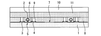
- FIG. 8 is a cross-sectional view showing the method for manufacturing the semiconductor device according to the first embodiment.
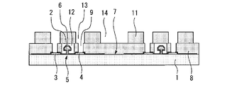
- FIG. 8 is a cross-sectional view showing the method for manufacturing the semiconductor device according to the first embodiment.
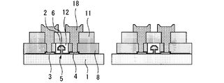
- FIG. 8 is a cross-sectional view showing the method for manufacturing the semiconductor device according to the first embodiment.
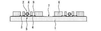
- FIG. 8 is a cross-sectional view showing the method for manufacturing the semiconductor device according to the first embodiment.
- FIG. 8 is a cross-sectional view showing the method for manufacturing the semiconductor device according to the first embodiment.
- FIG. 8 is a cross-sectional view showing the method for manufacturing the semiconductor device according to the first embodiment.
- FIG. 8 is a cross-sectional view showing the method for manufacturing the semiconductor device according to the first embodiment.
- FIG. 8 is a cross-sectional view showing the method for manufacturing the semiconductor device according to the first embodiment.
- FIG. 8 is a cross-sectional view showing the method for manufacturing the semiconductor device according to the first embodiment.
- FIG. 8 is a cross-sectional view showing the method for manufacturing the semiconductor device according to the first embodiment.
- FIG. It is sectional drawing which shows the manufacturing method of the semiconductor device which concerns on a comparative example. It is sectional drawing which shows the manufacturing method of the semiconductor device which concerns on a comparative example. It is sectional drawing which shows the manufacturing method of the semiconductor device which concerns on a comparative example.
- FIG. 10 is a cross-sectional view showing the method for manufacturing the semiconductor device according to the second embodiment.
- FIG. 10 is a cross-sectional view showing the method for manufacturing the semiconductor device according to the second embodiment.
- FIG. 10 is a cross-sectional view showing the method for manufacturing the semiconductor device according to the second embodiment.
- FIG. 10 is a cross-sectional view showing the method for manufacturing the semiconductor device according to the third embodiment.
- FIG. 10 is a cross-sectional view showing the method for manufacturing the semiconductor device according to the third embodiment.
- FIG. 10 is a cross-sectional view showing the method for manufacturing the semiconductor device according to the third embodiment.
- FIG. 10 is a cross-sectional view showing the method for manufacturing the semiconductor device according to the third embodiment.
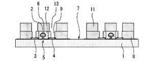
- FIG. 1 to 9 are cross-sectional views illustrating the method of manufacturing the semiconductor device according to the first embodiment.
- a semiconductor device 5 having a gate electrode 2, a source electrode 3 and a drain electrode 4 is formed on the main surface of a semiconductor substrate 1.
- the semiconductor device 5 is covered with an insulating film 6 having high moisture resistance.
- the insulating film 6 on the source electrode 3, the drain electrode 4 and the dicing line 7 is opened.
- a photosensitive resin film 8 covering the semiconductor device 5 and the dicing line 7 of the semiconductor substrate 1 is applied on the main surface of the semiconductor substrate 1 by a spin coater.
- the photosensitive resin film 8 is patterned by exposure and development, and the photosensitive resin film 8 around the gate electrode 2 is removed without removing the photosensitive resin film 8 on the dicing line 7.
- the photosensitive resin film 8 on the drain electrode 4 is removed to form a first contact hole 9. Then, the thermosetting process is performed and the photosensitive resin film 8 is hardened.
- the photosensitive resin film 11 supported by the support film 10 is attached to the upper surface of the photosensitive resin film 8 by using a lamination method or an STP method.
- the photosensitive resin film 11 covers the gate electrode 2, the source electrode 3, and the drain electrode 4 while being separated from the gate electrode 2, the source electrode 3, and the drain electrode 4.
- the support film 10 is peeled from the photosensitive resin film 11. Thereby, as shown in FIG. 4, a hollow structure 12 is formed around the gate electrode 2.
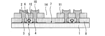
- the photosensitive resin film 11 is patterned by exposure and development to form a second contact hole 13 connected to the first contact hole 9 and a first opening 14 above the dicing line 7. Are formed at the same time. Then, the thermosetting process is performed and the photosensitive resin film 11 is hardened.
- an insulating film 15 and a resist 16 are sequentially formed on the entire surface, and the resist 16 is opened above the dicing line 7.
- dry etching is performed using the resist 16 as a mask.
- the insulating film 15 and the photosensitive resin film 8 on the dicing line 7 are removed to form the second opening 17.
- the thickness of the film to be removed by dry etching becomes thin, so that dry etching becomes easy.
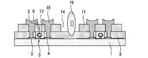
- the insulating film 15 and the resist 16 used as a mask are removed.
- a wiring 18 connected to the source electrode 3 and the drain electrode 4 through the first and second contact holes 9 and 13 is formed by plating or vapor deposition.
- the semiconductor substrate 1 is diced along the dicing line 7 using a dicing blade 19. As a result, as shown in FIG. 9, each chip is separated.
- 10 to 12 are cross-sectional views illustrating a method for manufacturing a semiconductor device according to a comparative example.
- the photosensitive resin film 8 on the dicing line 7 is removed when the photosensitive resin film 8 is patterned.
- the photosensitive resin film 11 is attached to the upper surface of the photosensitive resin film 8.
- the photosensitive resin film 11 is exposed and developed.
- the contact area between the photosensitive resin film 11 and the photosensitive resin film 8 is reduced by removing the photosensitive resin film 8 on the dicing line 7, the adhesion is weakened. For this reason, when peeling the support film 10 from the photosensitive resin film 11, the photosensitive resin film 11 may float or peel off. Moreover, the attached photosensitive resin film 11 may be embedded in the hollow part. As a result, there is a problem that the yield of the product is lowered.
- the photosensitive resin film 8 on the dicing line 7 is not removed when the photosensitive resin film 8 is patterned. For this reason, since the contact area of the photosensitive resin film 11 and the photosensitive resin film 8 increases, adhesive force improves and it can prevent the photosensitive resin film 11 from floating and peeling. Moreover, since the photosensitive resin film 11 is firmly supported by the photosensitive resin film 8, embedding can also be prevented. As a result, the product yield can be improved.
- the gate electrode 2 is a Y-type or T-type gate electrode including a eave, and a hollow structure 12 is also formed under the eaves of the gate electrode 2. As a result, the parasitic capacitance is reduced and the gain of the high frequency characteristics is improved.
- the photosensitive resin film 8 on the dicing line 7 is removed to form the second opening 17. Thereby, dicing becomes easy.
- the end of the first opening 14 of the photosensitive resin film 11 is closer to the semiconductor device 5 than the end of the second opening 17 of the photosensitive resin film 8. Thereby, it is possible to prevent the dicing blade from hitting the end of the first opening 14 of the photosensitive resin film 11 during the dicing line. For this reason, the yield of the semiconductor device is improved.
- FIG. 13 and 14 are cross-sectional views illustrating the method of manufacturing the semiconductor device according to the second embodiment.
- the process up to the process of FIG. 5 is the same as that of the first embodiment.
- the photosensitive resin film 8 on the dicing line 7 is not processed by dry etching, and the source electrode 3 and the drain are connected through the first and second contact holes 9 and 13 as shown in FIG. A wiring 18 connected to the electrode 4 is formed.
- the photosensitive resin film 8 on the dicing line 7 is diced together with the semiconductor substrate 1. Thereby, the number of processes can be reduced as compared with the first embodiment. Other configurations and effects are the same as those of the first embodiment.
- FIG. 15 to 18 are cross-sectional views illustrating the method of manufacturing the semiconductor device according to the third embodiment.
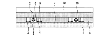
- the photosensitive resin film 11 of the first and second embodiments is replaced with a non-photosensitive resin film 19.
- the process up to the process of FIG. 5 is the same as that of the first embodiment.
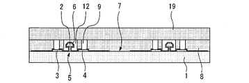
- a non-photosensitive resin film 19 supported by the support film 10 is attached to the upper surface of the photosensitive resin film 8 using a lamination method or an STP method.
- the non-photosensitive resin film 19 covers the gate electrode 2, the source electrode 3, and the drain electrode 4 while being separated from the gate electrode 2, the source electrode 3, and the drain electrode 4.
- a hollow structure 12 is formed around the gate electrode 2 as shown in FIG.
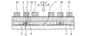
- an insulating film 15 and a resist 16 are sequentially formed on the entire surface, and the resist 16 is patterned by photolithography or the like.
- the resist 16 is patterned by photolithography or the like.
- the element structure is manufactured by performing either step of the first embodiment or the second embodiment.
- Other configurations and effects are the same as those of the first embodiment.
Landscapes
- Dicing (AREA)
- Internal Circuitry In Semiconductor Integrated Circuit Devices (AREA)
- Junction Field-Effect Transistors (AREA)
- Electrodes Of Semiconductors (AREA)
Abstract
Description
図1から図9は、実施の形態1に係る半導体装置の製造方法を示す断面図である。まず、図1に示すように、半導体基板1の主面にゲート電極2、ソース電極3及びドレイン電極4を有する半導体デバイス5を形成する。半導体デバイス5を耐湿性の高い絶縁膜6で覆う。ソース電極3、ドレイン電極4及びダイシングライン7上の絶縁膜6を開口する。次に、半導体デバイス5及び半導体基板1のダイシングライン7を覆う感光性樹脂膜8を半導体基板1の主面の上にスピンコータで塗布する。感光性樹脂膜8を露光及び現像によりパターニングして、ダイシングライン7の上の感光性樹脂膜8を除去することなく、ゲート電極2の周りの感光性樹脂膜8を除去し、ソース電極3及びドレイン電極4の上の感光性樹脂膜8を除去して第1のコンタクトホール9を形成する。その後、熱硬化処理を行って感光性樹脂膜8を硬化する。
図13及び図14は、実施の形態2に係る半導体装置の製造方法を示す断面図である。図5の工程までは実施の形態1と同様である。本実施の形態ではダイシングライン7の上の感光性樹脂膜8をドライエッチングで加工することなく、図13に示すように第1及び第2のコンタクトホール9,13を介してソース電極3及びドレイン電極4に接続された配線18を形成する。次に、図14に示すように、ダイシングライン7の上の感光性樹脂膜8を半導体基板1と共にダイシングする。これにより、実施の形態1よりもプロセス数を削減することができる。その他の構成及び効果は実施の形態1と同様である。
図15から図18は、実施の形態3に係る半導体装置の製造方法を示す断面図である。本実施の形態は、実施の形態1及び2の感光樹脂フィルム11を非感光性樹脂フィルム19に置き換えたものである。図5の工程までは実施の形態1と同様である。次に、図15に示すように、ラミネート法又はSTP法を用いて、支持フィルム10に支持された非感光性樹脂フィルム19を感光性樹脂膜8の上面に貼り付ける。非感光性樹脂フィルム19は、ゲート電極2、ソース電極3及びドレイン電極4から離間しつつゲート電極2、ソース電極3及びドレイン電極4の上方を覆う。次に、非感光性樹脂フィルム19から支持フィルム10を剥がすと、図16に示すように、ゲート電極2の周りに中空構造12が形成される。次に、図17に示すように、全面に絶縁膜15及びレジスト16を順に形成し、レジスト16をフォトリソグラフィ等によりパターニングする。このレジスト16をマスクとして用いたドライエッチングを行うことにより、図18に示すように、第2のコンタクトホール13及び第1の開口14を開口する。その後、実施の形態1又は実施の形態2のどちらかの工程を行って素子構造を作製する。その他の構成及び効果は実施の形態1と同様である。
Claims (6)
- 半導体基板の主面に第1及び第2の電極を有する半導体デバイスを形成する工程と、
前記半導体デバイス及び前記半導体基板のダイシングラインを覆う樹脂膜を前記半導体基板の前記主面の上に形成し、前記ダイシングラインの上の前記樹脂膜を除去することなく前記第1の電極の周りの前記樹脂膜を除去し前記第2の電極の上の前記樹脂膜を除去して第1のコンタクトホールを形成する工程と、
前記第1及び第2の電極から離間しつつ前記第1及び第2の電極の上方を覆う樹脂フィルムを前記樹脂膜の上面に貼り付けて前記第1の電極の周りに中空構造を形成する工程と、
前記樹脂フィルムをパターニングして、前記第1のコンタクトホールにつながる第2のコンタクトホールと前記ダイシングラインの上方の第1の開口を同時に形成する工程と、
前記第1及び第2のコンタクトホールを介して前記第2の電極に接続された配線を形成する工程と、
前記第1の開口を形成した後に前記ダイシングラインに沿って前記半導体基板をダイシングする工程とを備えることを特徴とする半導体装置の製造方法。 - 支持フィルムに支持された前記樹脂フィルムを前記樹脂膜の上面に貼り付けた後に前記樹脂フィルムから前記支持フィルムを剥がすことを特徴とする請求項1に記載の半導体装置の製造方法。
- 前記第1の電極はひさしを含むY型又はT型のゲート電極であり、
前記ゲート電極の前記ひさしの下にも前記中空構造が形成されていることを特徴とする請求項1又は2に記載の半導体装置の製造方法。 - 前記第1の開口を形成した後、前記半導体基板をダイシングする前に前記ダイシングラインの上の前記樹脂膜を除去して第2の開口を形成する工程を更に備えることを特徴とする請求項1~3の何れか1項に記載の半導体装置の製造方法。
- 前記第1の開口の端部が前記第2の開口の端部よりも前記半導体デバイス側であることを特徴とする請求項4に記載の半導体装置の製造方法。
- 前記ダイシングラインの上の前記樹脂膜を前記半導体基板と共にダイシングすることを特徴とする請求項1~3の何れか1項に記載の半導体装置の製造方法。
Priority Applications (7)
| Application Number | Priority Date | Filing Date | Title |
|---|---|---|---|
| US16/959,369 US11244863B2 (en) | 2018-05-28 | 2018-05-28 | Method for manufacturing semiconductor apparatus |
| CN201880093695.9A CN112189251B (zh) | 2018-05-28 | 2018-05-28 | 半导体装置的制造方法 |
| KR1020207033211A KR102497370B1 (ko) | 2018-05-28 | 2018-05-28 | 반도체 장치의 제조 방법 |
| PCT/JP2018/020353 WO2019229802A1 (ja) | 2018-05-28 | 2018-05-28 | 半導体装置の製造方法 |
| DE112018007677.6T DE112018007677B4 (de) | 2018-05-28 | 2018-05-28 | Verfahren zur Herstellung eines Halbleitergerätes |
| JP2020521653A JP6927430B2 (ja) | 2018-05-28 | 2018-05-28 | 半導体装置の製造方法 |
| TW107129787A TWI683357B (zh) | 2018-05-28 | 2018-08-27 | 半導體裝置之製造方法 |
Applications Claiming Priority (1)
| Application Number | Priority Date | Filing Date | Title |
|---|---|---|---|
| PCT/JP2018/020353 WO2019229802A1 (ja) | 2018-05-28 | 2018-05-28 | 半導体装置の製造方法 |
Publications (1)
| Publication Number | Publication Date |
|---|---|
| WO2019229802A1 true WO2019229802A1 (ja) | 2019-12-05 |
Family
ID=68697057
Family Applications (1)
| Application Number | Title | Priority Date | Filing Date |
|---|---|---|---|
| PCT/JP2018/020353 Ceased WO2019229802A1 (ja) | 2018-05-28 | 2018-05-28 | 半導体装置の製造方法 |
Country Status (7)
| Country | Link |
|---|---|
| US (1) | US11244863B2 (ja) |
| JP (1) | JP6927430B2 (ja) |
| KR (1) | KR102497370B1 (ja) |
| CN (1) | CN112189251B (ja) |
| DE (1) | DE112018007677B4 (ja) |
| TW (1) | TWI683357B (ja) |
| WO (1) | WO2019229802A1 (ja) |
Cited By (1)
| Publication number | Priority date | Publication date | Assignee | Title |
|---|---|---|---|---|
| JP2025100771A (ja) * | 2020-05-08 | 2025-07-03 | ローム株式会社 | 半導体装置 |
Families Citing this family (2)
| Publication number | Priority date | Publication date | Assignee | Title |
|---|---|---|---|---|
| DE212021000199U1 (de) * | 2020-05-08 | 2022-02-07 | Rohm Co. Ltd | Halbleiterbauteil |
| CN117334566A (zh) * | 2022-06-24 | 2024-01-02 | 长鑫存储技术有限公司 | 半导体结构及其形成方法、版图结构 |
Citations (3)
| Publication number | Priority date | Publication date | Assignee | Title |
|---|---|---|---|---|
| JP2009206183A (ja) * | 2008-02-26 | 2009-09-10 | Fujitsu Media Device Kk | 電子部品及びその製造方法 |
| JP2011014652A (ja) * | 2009-06-30 | 2011-01-20 | Panasonic Electric Works Co Ltd | 機能性デバイスの製造方法および、それにより製造された機能性デバイスを用いた半導体装置の製造方法 |
| JP2016039319A (ja) * | 2014-08-08 | 2016-03-22 | 三菱電機株式会社 | 半導体装置の製造方法 |
Family Cites Families (20)
| Publication number | Priority date | Publication date | Assignee | Title |
|---|---|---|---|---|
| JPH05335343A (ja) * | 1992-05-27 | 1993-12-17 | Sony Corp | 電界効果トランジスタ |
| JP2004147220A (ja) | 2002-10-25 | 2004-05-20 | Toyo Commun Equip Co Ltd | Sawチップの構造、その製造方法、表面実装型sawデバイス、及びその製造方法 |
| JP2005150452A (ja) * | 2003-11-17 | 2005-06-09 | Fujikura Ltd | 半導体パッケージの製造方法 |
| JP3953027B2 (ja) * | 2003-12-12 | 2007-08-01 | ソニー株式会社 | 半導体装置およびその製造方法 |
| JP4413062B2 (ja) * | 2004-04-13 | 2010-02-10 | シャープ株式会社 | パターニングされた膜を有する基板の製造方法 |
| JP2006093367A (ja) * | 2004-09-24 | 2006-04-06 | Sanyo Electric Co Ltd | 半導体装置の製造方法 |
| JP4607531B2 (ja) * | 2004-09-29 | 2011-01-05 | カシオマイクロニクス株式会社 | 半導体装置の製造方法 |
| JP2006278610A (ja) * | 2005-03-29 | 2006-10-12 | Sanyo Electric Co Ltd | 半導体装置及びその製造方法 |
| US7807506B2 (en) | 2006-02-03 | 2010-10-05 | Infineon Technologies Ag | Microelectromechanical semiconductor component with cavity structure and method for producing the same |
| KR20090063983A (ko) * | 2007-12-14 | 2009-06-18 | 주식회사 코오롱 | 칩온필름용 적층필름 및 칩온필름의 제조방법 |
| JP4939452B2 (ja) * | 2008-02-07 | 2012-05-23 | ラピスセミコンダクタ株式会社 | 半導体装置の製造方法 |
| JP5335343B2 (ja) * | 2008-09-18 | 2013-11-06 | 株式会社アルバック | 付着物の分析方法 |
| JP2013065582A (ja) * | 2009-12-28 | 2013-04-11 | Fujikura Ltd | 半導体ウエハ及び半導体装置並びに半導体装置の製造方法 |
| JP5799952B2 (ja) | 2010-05-20 | 2015-10-28 | 日立化成株式会社 | 感光性樹脂組成物、感光性フィルム、リブパターンの形成方法、中空構造とその形成方法及び電子部品 |
| JP5521862B2 (ja) * | 2010-07-29 | 2014-06-18 | 三菱電機株式会社 | 半導体装置の製造方法 |
| JP5821429B2 (ja) * | 2011-09-01 | 2015-11-24 | 三菱電機株式会社 | 半導体装置及びその製造方法 |
| US9613930B2 (en) * | 2013-10-25 | 2017-04-04 | Infineon Technologies Ag | Semiconductor device and method for manufacturing a semiconductor device |
| JP2015106698A (ja) * | 2013-12-02 | 2015-06-08 | 味の素株式会社 | 半導体装置の製造方法 |
| TWI657510B (zh) * | 2014-10-02 | 2019-04-21 | 日商住友電木股份有限公司 | 半導體裝置之製造方法及半導體裝置 |
| US9748334B1 (en) * | 2016-02-18 | 2017-08-29 | International Business Machines Corporation | Fabrication of nanomaterial T-gate transistors with charge transfer doping layer |
-
2018
- 2018-05-28 CN CN201880093695.9A patent/CN112189251B/zh active Active
- 2018-05-28 WO PCT/JP2018/020353 patent/WO2019229802A1/ja not_active Ceased
- 2018-05-28 JP JP2020521653A patent/JP6927430B2/ja active Active
- 2018-05-28 US US16/959,369 patent/US11244863B2/en active Active
- 2018-05-28 DE DE112018007677.6T patent/DE112018007677B4/de active Active
- 2018-05-28 KR KR1020207033211A patent/KR102497370B1/ko active Active
- 2018-08-27 TW TW107129787A patent/TWI683357B/zh active
Patent Citations (3)
| Publication number | Priority date | Publication date | Assignee | Title |
|---|---|---|---|---|
| JP2009206183A (ja) * | 2008-02-26 | 2009-09-10 | Fujitsu Media Device Kk | 電子部品及びその製造方法 |
| JP2011014652A (ja) * | 2009-06-30 | 2011-01-20 | Panasonic Electric Works Co Ltd | 機能性デバイスの製造方法および、それにより製造された機能性デバイスを用いた半導体装置の製造方法 |
| JP2016039319A (ja) * | 2014-08-08 | 2016-03-22 | 三菱電機株式会社 | 半導体装置の製造方法 |
Cited By (2)
| Publication number | Priority date | Publication date | Assignee | Title |
|---|---|---|---|---|
| JP2025100771A (ja) * | 2020-05-08 | 2025-07-03 | ローム株式会社 | 半導体装置 |
| JP7850846B2 (ja) | 2020-05-08 | 2026-04-23 | ローム株式会社 | 半導体装置 |
Also Published As
| Publication number | Publication date |
|---|---|
| US20210066128A1 (en) | 2021-03-04 |
| TW202004870A (zh) | 2020-01-16 |
| TWI683357B (zh) | 2020-01-21 |
| KR102497370B1 (ko) | 2023-02-07 |
| DE112018007677T5 (de) | 2021-03-04 |
| JPWO2019229802A1 (ja) | 2021-02-12 |
| JP6927430B2 (ja) | 2021-08-25 |
| CN112189251B (zh) | 2023-12-26 |
| US11244863B2 (en) | 2022-02-08 |
| CN112189251A (zh) | 2021-01-05 |
| DE112018007677B4 (de) | 2023-10-12 |
| KR20200143481A (ko) | 2020-12-23 |
Similar Documents
| Publication | Publication Date | Title |
|---|---|---|
| CN112039458B (zh) | 体声波谐振器的封装方法及封装结构 | |
| CN112039459B (zh) | 体声波谐振器的封装方法及封装结构 | |
| US8748320B2 (en) | Connection to first metal layer in thin film transistor process | |
| KR100779869B1 (ko) | 전자 부품 및 제조 방법 | |
| US8129835B2 (en) | Package substrate having semiconductor component embedded therein and fabrication method thereof | |
| JP6927430B2 (ja) | 半導体装置の製造方法 | |
| CN105374743A (zh) | 半导体装置的制造方法 | |
| JP6370515B1 (ja) | 半導体装置およびその製造方法 | |
| TWI631782B (zh) | 半導體雷射及其製造方法 | |
| TWI437689B (zh) | 半導體裝置 | |
| CN106129026B (zh) | 半导体结构及其制作方法 | |
| TWI697078B (zh) | 封裝基板結構與其接合方法 | |
| JPH11186393A (ja) | 半導体素子及びその製造方法 | |
| CN118116897A (zh) | 半导体装置及半导体装置的制造方法 | |
| JP6757293B2 (ja) | 化合物半導体集積回路及びその作製方法 | |
| JP2005302816A (ja) | 半導体装置及びその製造方法 | |
| JP4829161B2 (ja) | 半導体装置の製造方法 | |
| JP7566508B2 (ja) | 半導体装置及び半導体装置の製造方法 | |
| JP3003394B2 (ja) | 突起電極の製造方法 | |
| JP6341336B2 (ja) | 薄膜素子およびその製造方法 | |
| JP4984645B2 (ja) | 半導体装置の製造方法 | |
| KR100914978B1 (ko) | 반도체 소자 및 그의 제조 방법 | |
| JP2006114760A (ja) | 薄膜キャパシタ素子およびその製造方法 | |
| JPH1022384A (ja) | 半導体装置およびその製造方法 | |
| JPH11251482A (ja) | 半導体装置及びその製造方法 |
Legal Events
| Date | Code | Title | Description |
|---|---|---|---|
| 121 | Ep: the epo has been informed by wipo that ep was designated in this application |
Ref document number: 18920359 Country of ref document: EP Kind code of ref document: A1 |
|
| ENP | Entry into the national phase |
Ref document number: 2020521653 Country of ref document: JP Kind code of ref document: A |
|
| ENP | Entry into the national phase |
Ref document number: 20207033211 Country of ref document: KR Kind code of ref document: A |
|
| 122 | Ep: pct application non-entry in european phase |
Ref document number: 18920359 Country of ref document: EP Kind code of ref document: A1 |